KR100589498B1 - Semiconductor device and manufacturing method thereof - Google Patents
Semiconductor device and manufacturing method thereofDownload PDFInfo
- Publication number
- KR100589498B1 KR100589498B1KR1020030041481AKR20030041481AKR100589498B1KR 100589498 B1KR100589498 B1KR 100589498B1KR 1020030041481 AKR1020030041481 AKR 1020030041481AKR 20030041481 AKR20030041481 AKR 20030041481AKR 100589498 B1KR100589498 B1KR 100589498B1
- Authority
- KR
- South Korea
- Prior art keywords
- gate electrode
- substrate
- film
- nitride film
- sidewall
- Prior art date
- Legal status (The legal status is an assumption and is not a legal conclusion. Google has not performed a legal analysis and makes no representation as to the accuracy of the status listed.)
- Expired - Fee Related
Links
Images


Classifications
- H—ELECTRICITY
- H10—SEMICONDUCTOR DEVICES; ELECTRIC SOLID-STATE DEVICES NOT OTHERWISE PROVIDED FOR
- H10D—INORGANIC ELECTRIC SEMICONDUCTOR DEVICES
- H10D84/00—Integrated devices formed in or on semiconductor substrates that comprise only semiconducting layers, e.g. on Si wafers or on GaAs-on-Si wafers
- H10D84/01—Manufacture or treatment
- H10D84/0123—Integrating together multiple components covered by H10D12/00 or H10D30/00, e.g. integrating multiple IGBTs
- H10D84/0126—Integrating together multiple components covered by H10D12/00 or H10D30/00, e.g. integrating multiple IGBTs the components including insulated gates, e.g. IGFETs
- H10D84/0147—Manufacturing their gate sidewall spacers
- H—ELECTRICITY
- H01—ELECTRIC ELEMENTS
- H01L—SEMICONDUCTOR DEVICES NOT COVERED BY CLASS H10
- H01L21/00—Processes or apparatus adapted for the manufacture or treatment of semiconductor or solid state devices or of parts thereof
- H01L21/70—Manufacture or treatment of devices consisting of a plurality of solid state components formed in or on a common substrate or of parts thereof; Manufacture of integrated circuit devices or of parts thereof
- H01L21/71—Manufacture of specific parts of devices defined in group H01L21/70
- H01L21/768—Applying interconnections to be used for carrying current between separate components within a device comprising conductors and dielectrics
- H01L21/76801—Applying interconnections to be used for carrying current between separate components within a device comprising conductors and dielectrics characterised by the formation and the after-treatment of the dielectrics, e.g. smoothing
- H01L21/76829—Applying interconnections to be used for carrying current between separate components within a device comprising conductors and dielectrics characterised by the formation and the after-treatment of the dielectrics, e.g. smoothing characterised by the formation of thin functional dielectric layers, e.g. dielectric etch-stop, barrier, capping or liner layers
- H01L21/76834—Applying interconnections to be used for carrying current between separate components within a device comprising conductors and dielectrics characterised by the formation and the after-treatment of the dielectrics, e.g. smoothing characterised by the formation of thin functional dielectric layers, e.g. dielectric etch-stop, barrier, capping or liner layers formation of thin insulating films on the sidewalls or on top of conductors
- H—ELECTRICITY
- H01—ELECTRIC ELEMENTS
- H01L—SEMICONDUCTOR DEVICES NOT COVERED BY CLASS H10
- H01L21/00—Processes or apparatus adapted for the manufacture or treatment of semiconductor or solid state devices or of parts thereof
- H01L21/70—Manufacture or treatment of devices consisting of a plurality of solid state components formed in or on a common substrate or of parts thereof; Manufacture of integrated circuit devices or of parts thereof
- H01L21/71—Manufacture of specific parts of devices defined in group H01L21/70
- H01L21/768—Applying interconnections to be used for carrying current between separate components within a device comprising conductors and dielectrics
- H01L21/76801—Applying interconnections to be used for carrying current between separate components within a device comprising conductors and dielectrics characterised by the formation and the after-treatment of the dielectrics, e.g. smoothing
- H01L21/76837—Filling up the space between adjacent conductive structures; Gap-filling properties of dielectrics
- H—ELECTRICITY
- H10—SEMICONDUCTOR DEVICES; ELECTRIC SOLID-STATE DEVICES NOT OTHERWISE PROVIDED FOR
- H10D—INORGANIC ELECTRIC SEMICONDUCTOR DEVICES
- H10D84/00—Integrated devices formed in or on semiconductor substrates that comprise only semiconducting layers, e.g. on Si wafers or on GaAs-on-Si wafers
- H10D84/01—Manufacture or treatment
- H10D84/0123—Integrating together multiple components covered by H10D12/00 or H10D30/00, e.g. integrating multiple IGBTs
- H10D84/0126—Integrating together multiple components covered by H10D12/00 or H10D30/00, e.g. integrating multiple IGBTs the components including insulated gates, e.g. IGFETs
- H10D84/013—Manufacturing their source or drain regions, e.g. silicided source or drain regions
Landscapes
- Engineering & Computer Science (AREA)
- Physics & Mathematics (AREA)
- Condensed Matter Physics & Semiconductors (AREA)
- General Physics & Mathematics (AREA)
- Manufacturing & Machinery (AREA)
- Computer Hardware Design (AREA)
- Microelectronics & Electronic Packaging (AREA)
- Power Engineering (AREA)
- Insulated Gate Type Field-Effect Transistor (AREA)
Abstract
Translated fromKoreanDescription
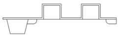
Translated fromKorean도 1은 종래기술에 의한 반도체 제조 방법.1 is a semiconductor manufacturing method according to the prior art.
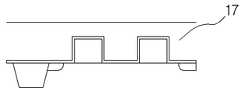
도 2는 본 발명에 의한 반도체 제조 방법.2 is a semiconductor manufacturing method according to the present invention.
본 발명은 층간 절연막의 갭필 능력을 향상시키기 위하여 측벽 삼중 구조를 이용하여 소오스/드레인 이온주입시 하부 기판의 Si 데미지를 방지하기 위해 진행하는 캡핑 절연막과 콘택 에치시 마진을 확보하기 위하여 형성된 질화막을 측벽에 남아있는 질화막으로 대체하는 반도체 소자의 제조방법에 관한 것이다.The present invention uses a sidewall triple structure to improve the gap fill capability of the interlayer insulating film, and a sidewall of the nitride film formed to secure a margin during contact etch and a capping insulating film that proceeds to prevent Si damage of the lower substrate during source / drain ion implantation. The present invention relates to a method for manufacturing a semiconductor device which is replaced with a nitride film remaining on the substrate.
최근, DRAM 장치의 직접도가 증가되면서 칩 사이즈 및 디자인 룰(Design Rule)이 작아짐으로 인하여 워드라인 사이에 형성되는 절연막에 보이드(Void)가 발생된다. 메모리 콘택을 형성하기 위한 이후 공정에서 도전성 물질의 증착시에 상기 보이드에도 도전성 물질이 형성됨에 따라 메모리 콘택간에 숏트(Short) 현상이 발 생되어 반도체 소자의 생산 수율(yield)을 저하시키는 원인이 되고 있다.Recently, as the directivity of a DRAM device increases, voids are generated in an insulating film formed between word lines due to a decrease in chip size and a design rule. As the conductive material is also formed in the voids during the deposition of the conductive material in a subsequent process for forming a memory contact, a short phenomenon occurs between the memory contacts, causing a decrease in the yield of the semiconductor device. have.
이하, 첨부된 도면을 참조하여 종래 반도체 소자의 제조방법을 설명하면 다음과 같다.Hereinafter, a manufacturing method of a conventional semiconductor device will be described with reference to the accompanying drawings.
도 1a 내지 도 1d는 종래 반도체 소자의 제조공정 단면도이다.1A to 1D are cross-sectional views of a manufacturing process of a conventional semiconductor device.
우선, 도 1a에 도시된 바와 같이 소자 분리막(1)이 형성된 반도체 기판의 표면에 게이트 산화막(도시하지 않았음)을 형성하고 상기 게이트 산화막상에 폴리실리콘막을 형성한 후에 포토 및 식각 공정으로 상기 폴리실리콘막을 선택적으로 제거하여 반도체 기판상에 일방향으로 정렬되는 복수개의 게이트 전극(2)을 형성한다. 후에 캡핑 절연막(3)을 열 산화공정으로 형성후 질화막(4)을 증착한다.First, as shown in FIG. 1A, a gate oxide film (not shown) is formed on a surface of a semiconductor substrate on which the
이어, 도 1b에 도시된 바와 같이 상기 질화막을 에치백(Etch-back)하여 측벽(5)을 형성한다. 후에 이온주입 공정으로 소오스/드레인(Source/Drain; 이하 S/D) 불순물 영영(6)을 형성한다.Subsequently, as illustrated in FIG. 1B, the nitride layer is etched back to form
이어, 도 1c에 도시된 바와 같이 S/D영역이 형성된 기판에 질화막을 형성한다. 상기 질화막은 소자분리막의 스파이킹 방지를 위해 형성한다.Next, as shown in FIG. 1C, a nitride film is formed on the substrate on which the S / D region is formed. The nitride layer is formed to prevent spikes of the device isolation layer.
그리고, 도 1d에 도시된 바와 같이 상기 게이트 전극 사이의 공간이 채워지도록 상기 기판의 전면에 BPSG(Boron Phosphorus Silicate Glass)막을 증착하여 갭필(gap fill)막(8)을 형성하고, CMP(Chemical Mechanical Polishing) 공정으로 상기 갭필막의 표면을 평탄화한다.As shown in FIG. 1D, a BPSG (Boron Phosphorus Silicate Glass) film is deposited on the entire surface of the substrate to fill the space between the gate electrodes to form a
상기 갭필막을 형성할 때에 상기 게이트 전극 사이의 공간이 매우 좁기 때문에 상기 게이트 전극 사이에 형성되는 상기 갭필막에 보이드(9)가 발생하는 문제점 이 있다. 상기 보이드는 상기 게이트 전극 사이의 상기 갭필막 내에 상기 게이트 전극과 나란한 방향으로 발생된다.Since the space between the gate electrodes is very narrow when forming the gap fill film, there is a problem that
따라서, 본 발명은 상기와 같은 종래 기술의 문제점을 해결하기 위한 것으로, 캡핑 절연막 및 라이너 질화막 공정을 따로 진행하지 않고 기 진행된 측벽 질화막을 사이드월 에치시 제어하여 질화막을 소정부분 남겨둠으로써 상기 질화막으로 위의 두가지 공정을 대체하는 반도체 소자의 제조방법을 제공함에 본 발명의 목적이 있다.
Accordingly, the present invention is to solve the problems of the prior art as described above, and the sidewall nitride film is controlled by sidewall etching without proceeding the capping insulating film and the liner nitride film process to leave a predetermined portion of the nitride film to the nitride film. It is an object of the present invention to provide a method of manufacturing a semiconductor device that replaces the above two processes.
본 발명의 상기 목적은 소정의 구조물이 형성된 기판에 폴리를 증착하고 패터닝하여 게이트 전극을 형성하는 단계, 상기 게이트 전극을 포함한 상기 기판 상부 전면에 질화막을 증착하는 단계, 상기 질화막 상부에 산화막을 증착하는 단계, 상기 산화막을 상기 게이트 전극 측벽에만 남도록 에치하여 사이드월을 형성하는 단계, 상기 게이트 전극과 사이드월을 마스크로 상기 기판에 이온을 주입하여 소오스/드레인 영역을 형성하는 단계 및 상기 사이드월을 제거한 후 상기 질화막 상부에 층간 절연막을 형성하는 단계를 포함하는 반도체 소자의 제조방법에 의해 달성된다.The object of the present invention is to form a gate electrode by depositing and patterning poly on a substrate on which a predetermined structure is formed, depositing a nitride film on the entire upper surface of the substrate including the gate electrode, depositing an oxide film on the nitride film Forming a sidewall by etching the oxide film so as to remain only on the sidewall of the gate electrode, implanting ions into the substrate using the gate electrode and the sidewall as a mask to form a source / drain region, and removing the sidewall And then forming an interlayer insulating film over the nitride film.
본 발명의 상기 목적은 기판 상부에 형성된 게이트 전극, 상기 게이트 전극 을 포함한 기판 전면에 형성된 질화막, 상기 질화막 상부에 형성된 층간 절연막 및 상기 게이트 전극에서 일정 간격 이격된 기판에 형성된 소오스/드레인 영역을 포함하는 반도체 소자에 의해서도 달성된다.The object of the present invention includes a gate electrode formed on the substrate, a nitride film formed on the front surface of the substrate including the gate electrode, an interlayer insulating film formed on the nitride film and source / drain regions formed on the substrate spaced apart from the gate electrode by a predetermined distance. It is also achieved by a semiconductor element.
본 발명의 상기 목적과 기술적 구성 및 그에 따른 작용효과에 관한 자세한 사항은 본 발명의 바람직한 실시예를 도시하고 있는 도면을 참조한 이하 상세한 설명에 의해 보다 명확하게 이해될 것이다.Details of the above object and technical configuration of the present invention and the effects thereof according to the present invention will be more clearly understood by the following detailed description with reference to the drawings showing preferred embodiments of the present invention.
본 발명에 따른 반도체 소자의 제조방법은 소정의 구조물이 형성된 기판에 폴리를 증착하고 패터닝하여 게이트 전극을 형성하는 단계, 상기 게이트 전극을 열산화하여 상기 게이트 전극 표면에 폴리 산화막을 형성하는 단계, 상기 반도체 기판에 저농도의 이온을 주입하여 LDD 영역을 형성하는 단계, 상기 게이트 전극을 포함한 상기 기판 상부 전면에 질화막을 증착하는 단계, 상기 질화막 상부에 산화막을 증착하는 단계, 상기 산화막을 상기 게이트 전극 측벽에만 남도록 에치하여 사이드월을 형성하는 단계, 상기 게이트 전극과 사이드월을 마스크로 상기 기판에 이온을 주입하여 소오스/드레인 영역을 형성하는 단계 및 상기 사이드월을 제거한 후 상기 질화막 상부에 층간 절연막을 형성하는 단계로 구성되어 있다.A method of manufacturing a semiconductor device according to the present invention comprises the steps of forming a gate electrode by depositing and patterning poly on a substrate having a predetermined structure, thermal oxidation of the gate electrode to form a poly oxide film on the gate electrode surface, the Implanting a low concentration of ions into a semiconductor substrate to form an LDD region, depositing a nitride film over the entire upper surface of the substrate including the gate electrode, depositing an oxide film over the nitride film, and depositing the oxide film only on the gate electrode sidewalls Forming a sidewall by etching the remaining sidewalls, implanting ions into the substrate using the gate electrode and the sidewall as a mask, forming a source / drain region, and forming an interlayer insulating layer on the nitride film after removing the sidewall. It consists of steps.
도 2a 내지 도 2d는 본 발명에 따른 반도체 소자의 제조공정 단면도이다.2A to 2D are cross-sectional views of a manufacturing process of a semiconductor device according to the present invention.
우선, 도 2a에 도시된 바와 같이 소자 분리막(11)이 형성된 반도체 기판의 표면에 게이트 산화막을 형성하고 상기 게이트 산화막상에 폴리실리콘막을 형성한 후에 포토 및 에치 공정으로 상기 폴리실리콘막을 선택적으로 제거하여 반도체 기판상에 일방향으로 정렬되는 복수개의 게이트 전극(12)을 형성한다. 이때, 상기 게 이트 전극(12)을 열산화하여 게이트 전극 표면에 폴리 산화막을 형성하고, 폴리 산화막이 형성된 게이트 전극을 마스크로 기판에 저농도의 이온을 주입하여 LDD 영역을 형성할 수도 있다.First, as shown in FIG. 2A, a gate oxide film is formed on a surface of a semiconductor substrate on which the
후에 질화막(13)과 산화막(14)을 순차적으로 형성한다.After that, the
상기 질화막은 300~500Å의 두께로 형성하는 것이 바람직하다.The nitride film is preferably formed to a thickness of 300 ~ 500Å.
상기 산화막은 700~900Å의 두께로 형성하는 것이 바람직하다.The oxide film is preferably formed to a thickness of 700 ~ 900Å.
2b에 도시된 바와 같이 상기 산화막에 에치공정을 진행하여 게이트 전극(12)의 측벽에 사이드월(15)을 형성한다. 후에 게이트 전극(12)과 사이드월(15)을 마스크로 기판에이온주입 공정으로 S/D 영역(16)을 형성한다.As shown in 2b, the
상기 사이드월을 형성하기 위하여 에치공정을 진행 시 상기 질화막을 엔드포인트(End point)를 이용해 에치공정을 진행하고 오버 에치시 질화막을 약 100Å정도 에치하여 최종적으로 남아있는 질화막의 두께가 200~400Å인 상태에서 S/D 이온 주입공정을 진행한다.When forming the sidewall, the nitride film is etched by using an end point when the etching process is performed, and the nitride film is etched by about 100Å when the overetch is about 200 ~ 400Å. S / D ion implantation process is performed in the state.
200~400Å의 두께로 남아있는 상기 질화막이 이온 주입시 발생하는 하부 기판의 실리콘 데미지를 방지하는 캡핑 절연막 역할을 하는 동시에 콘택의 가장자리 에치시 발생할 수 있는 STI 스파이킹 방지를 위한 역할도 하게 된다.The nitride film, which has a thickness of about 200 to about 400 microns, serves as a capping insulating film that prevents silicon damage of the lower substrate generated during ion implantation, and also serves to prevent STI spiking that may occur when the edge of the contact is etched.
이어, 도 2c에 도시된 바와 같이 상기 사이드월을 에치 공정을 이용하여 제거한다.Subsequently, the sidewalls are removed using an etch process as shown in FIG. 2C.
상기와 같이 제거된 사이드월에 의해 후속공정에서 층간절연막을 증착시 게이트 전극(12) 간의 간극이 넓어져서 보이드 현상이 발생하지 않는다.The sidewalls removed as described above widen the gap between the
그리고, 도 2d에 도시된 바와 같이 게이트 전극(12) 사이의 공간이 채워지도록 상기 기판의 전면에 BPSG막 또는 PSG막을 증착하여 절연막(17)을 형성하고, CMP 공정으로 상기 절연막의 표면을 평탄화한다.As shown in FIG. 2D, a BPSG film or a PSG film is deposited on the entire surface of the substrate to fill the space between the
상기 절연막을 증착시 사이드월 역할을 하는 상기 산화막이 전 공정에서 이미 제거되어 있기 때문에 게이트 전극 간의 사이가 넓어져서 보이드가 발생하는 현상은 나타나지 않는다.Since the oxide film, which acts as a sidewall when the insulating film is deposited, has already been removed in the previous process, voids do not appear due to widening between the gate electrodes.
상기의 공정으로 제조된 반도체 소자는 기판 상부에 형성된 게이트 전극, 상기 게이트 전극을 포함한 기판 전면에 형성된 질화막, 상기 질화막 상부에 형성된 층간 절연막 및 상기 게이트 전극에서 일정 간격 이격된 기판에 형성된 소오스/드레인 영역으로 구성되어 있고, 상기 게이트 전극 표면에는 폴리 산화막이, 상기 소오스/드레인 영역과 게이트 전극 사이의 기판에는 LDD 영역이 포함되어 구성되어 있다.The semiconductor device manufactured by the above process includes a gate electrode formed on the substrate, a nitride film formed on the entire surface of the substrate including the gate electrode, an interlayer insulating film formed on the nitride film, and a source / drain region formed on the substrate spaced apart from the gate electrode by a predetermined distance. And a poly oxide film on the surface of the gate electrode, and an LDD region on the substrate between the source / drain region and the gate electrode.
상세히 설명된 본 발명에 의하여 본 발명의 특징부를 포함하는 변화들 및 변형들이 당해 기술 분야에서 숙련된 보통의 사람들에게 명백히 쉬워질 것임이 자명하다. 본 발명의 그러한 변형들의 범위는 본 발명의 특징부를 포함하는 당해 기술 분야에 숙련된 통상의 지식을 가진 자들의 범위 내에 있으며, 그러한 변형들은 본 발명의 청구항의 범위 내에 있는 것으로 간주된다.It will be apparent that changes and modifications incorporating features of the invention will be readily apparent to those skilled in the art by the invention described in detail. It is intended that the scope of such modifications of the invention be within the scope of those of ordinary skill in the art including the features of the invention, and such modifications are considered to be within the scope of the claims of the invention.
따라서, 본 발명의 반도체 소자의 제조방법은 소스/드레인 영역을 형성하고 사이드월을 제거함으로서 게이트 전극 사이의 폭을 넓게하여 층간 절연막의 형성시 공정 마진을 확보할 수 있으며, 사이드월 형성 공정에서의 질화막을 이온 주입에 따른 기판 손상을 방지하기 위한 캡핑막 및 콘택 식각시 식각 방지막으로 사용할 수 있어 층간 절연막의 식각 방지막 형성 공정을 생략할 수 있어 공정을 간소화할 수 있을 뿐만 아니라 그에 따라 반도체 소자의 제작단가를 낮출수 있는 효과가 있다.Therefore, in the method of manufacturing a semiconductor device of the present invention, by forming a source / drain region and removing sidewalls, the width between gate electrodes can be widened to secure a process margin when forming an interlayer insulating film. The nitride film can be used as an anti-etching film during the capping and contact etching to prevent substrate damage due to ion implantation, thus eliminating the etch preventing film forming process of the interlayer insulating film, thereby simplifying the process and manufacturing the semiconductor device accordingly. It is effective to lower the unit price.
Claims (9)
Translated fromKoreanPriority Applications (1)
| Application Number | Priority Date | Filing Date | Title |
|---|---|---|---|
| KR1020030041481AKR100589498B1 (en) | 2003-06-25 | 2003-06-25 | Semiconductor device and manufacturing method thereof |
Applications Claiming Priority (1)
| Application Number | Priority Date | Filing Date | Title |
|---|---|---|---|
| KR1020030041481AKR100589498B1 (en) | 2003-06-25 | 2003-06-25 | Semiconductor device and manufacturing method thereof |
Publications (2)
| Publication Number | Publication Date |
|---|---|
| KR20050000891A KR20050000891A (en) | 2005-01-06 |
| KR100589498B1true KR100589498B1 (en) | 2006-06-13 |
Family
ID=37216763
Family Applications (1)
| Application Number | Title | Priority Date | Filing Date |
|---|---|---|---|
| KR1020030041481AExpired - Fee RelatedKR100589498B1 (en) | 2003-06-25 | 2003-06-25 | Semiconductor device and manufacturing method thereof |
Country Status (1)
| Country | Link |
|---|---|
| KR (1) | KR100589498B1 (en) |
Families Citing this family (1)
| Publication number | Priority date | Publication date | Assignee | Title |
|---|---|---|---|---|
| US9527408B2 (en) | 2015-03-31 | 2016-12-27 | Ford Global Technologies, Llc | Deployable thigh support in a vehicle seat |
Citations (4)
| Publication number | Priority date | Publication date | Assignee | Title |
|---|---|---|---|---|
| KR19990005478A (en)* | 1997-06-30 | 1999-01-25 | 김영환 | Method for forming contact hole in semiconductor device |
| JPH1197529A (en)* | 1997-09-16 | 1999-04-09 | Sony Corp | Manufacture of semiconductor device |
| KR19990039738A (en)* | 1997-11-14 | 1999-06-05 | 구본준 | Manufacturing Method of Semiconductor Device |
| KR20010057337A (en)* | 1999-12-22 | 2001-07-04 | 박종섭 | Method of fabricating semiconductor devices |
- 2003
- 2003-06-25KRKR1020030041481Apatent/KR100589498B1/ennot_activeExpired - Fee Related
Patent Citations (4)
| Publication number | Priority date | Publication date | Assignee | Title |
|---|---|---|---|---|
| KR19990005478A (en)* | 1997-06-30 | 1999-01-25 | 김영환 | Method for forming contact hole in semiconductor device |
| JPH1197529A (en)* | 1997-09-16 | 1999-04-09 | Sony Corp | Manufacture of semiconductor device |
| KR19990039738A (en)* | 1997-11-14 | 1999-06-05 | 구본준 | Manufacturing Method of Semiconductor Device |
| KR20010057337A (en)* | 1999-12-22 | 2001-07-04 | 박종섭 | Method of fabricating semiconductor devices |
Also Published As
| Publication number | Publication date |
|---|---|
| KR20050000891A (en) | 2005-01-06 |
Similar Documents
| Publication | Publication Date | Title |
|---|---|---|
| KR100450671B1 (en) | Method for fabricating semiconductor device having storage node contact plugs | |
| US6387765B2 (en) | Method for forming an extended metal gate using a damascene process | |
| US6297126B1 (en) | Silicon nitride capped shallow trench isolation method for fabricating sub-micron devices with borderless contacts | |
| US6274419B1 (en) | Trench isolation of field effect transistors | |
| US5950090A (en) | Method for fabricating a metal-oxide semiconductor transistor | |
| US6613621B2 (en) | Methods of forming self-aligned contact pads using a damascene gate process | |
| KR20120036185A (en) | Semiconductor device and method for manufacturing the same | |
| JP2001196564A (en) | Semiconductor device and manufacturing method thereof | |
| US7649218B2 (en) | Lateral MOS transistor and method for manufacturing thereof | |
| KR20000013397A (en) | Manufacturing method of trench isolation | |
| KR100281124B1 (en) | Semicon ductor and method for fabricating the same | |
| KR100377833B1 (en) | Semiconductor device with borderless contact structure and method of manufacturing the same | |
| US6130121A (en) | Method for fabricating a transistor | |
| US6458680B2 (en) | Method of fabricating contact pads of a semiconductor device | |
| KR20060042460A (en) | Transistor manufacturing method having recess channel of semiconductor device | |
| KR100589498B1 (en) | Semiconductor device and manufacturing method thereof | |
| KR20060073818A (en) | Contact manufacturing method of semiconductor device | |
| KR100520514B1 (en) | Method of manufacturing semiconductor device | |
| KR100307968B1 (en) | Method of forming interlevel dielectric layers of semiconductor device provided with plug-poly | |
| KR100345069B1 (en) | Method of forming polysilicon plug for semiconductor device | |
| KR100532770B1 (en) | Method for manufacturing the semiconductor device | |
| KR100486120B1 (en) | Method for forming of mos transistor | |
| KR20010011640A (en) | Method for forming plug-poly in semiconductor device | |
| KR19990005478A (en) | Method for forming contact hole in semiconductor device | |
| KR100574920B1 (en) | Semiconductor device having self-aligned contact and manufacturing method thereof |
Legal Events
| Date | Code | Title | Description |
|---|---|---|---|
| A201 | Request for examination | ||
| PA0109 | Patent application | St.27 status event code:A-0-1-A10-A12-nap-PA0109 | |
| PA0201 | Request for examination | St.27 status event code:A-1-2-D10-D11-exm-PA0201 | |
| D13-X000 | Search requested | St.27 status event code:A-1-2-D10-D13-srh-X000 | |
| R18-X000 | Changes to party contact information recorded | St.27 status event code:A-3-3-R10-R18-oth-X000 | |
| PG1501 | Laying open of application | St.27 status event code:A-1-1-Q10-Q12-nap-PG1501 | |
| D14-X000 | Search report completed | St.27 status event code:A-1-2-D10-D14-srh-X000 | |
| E902 | Notification of reason for refusal | ||
| PE0902 | Notice of grounds for rejection | St.27 status event code:A-1-2-D10-D21-exm-PE0902 | |
| P11-X000 | Amendment of application requested | St.27 status event code:A-2-2-P10-P11-nap-X000 | |
| P13-X000 | Application amended | St.27 status event code:A-2-2-P10-P13-nap-X000 | |
| E902 | Notification of reason for refusal | ||
| PE0902 | Notice of grounds for rejection | St.27 status event code:A-1-2-D10-D21-exm-PE0902 | |
| T11-X000 | Administrative time limit extension requested | St.27 status event code:U-3-3-T10-T11-oth-X000 | |
| P11-X000 | Amendment of application requested | St.27 status event code:A-2-2-P10-P11-nap-X000 | |
| P13-X000 | Application amended | St.27 status event code:A-2-2-P10-P13-nap-X000 | |
| E701 | Decision to grant or registration of patent right | ||
| PE0701 | Decision of registration | St.27 status event code:A-1-2-D10-D22-exm-PE0701 | |
| PN2301 | Change of applicant | St.27 status event code:A-3-3-R10-R13-asn-PN2301 St.27 status event code:A-3-3-R10-R11-asn-PN2301 | |
| PN2301 | Change of applicant | St.27 status event code:A-3-3-R10-R13-asn-PN2301 St.27 status event code:A-3-3-R10-R11-asn-PN2301 | |
| GRNT | Written decision to grant | ||
| PR0701 | Registration of establishment | St.27 status event code:A-2-4-F10-F11-exm-PR0701 | |
| PR1002 | Payment of registration fee | St.27 status event code:A-2-2-U10-U11-oth-PR1002 Fee payment year number:1 | |
| PG1601 | Publication of registration | St.27 status event code:A-4-4-Q10-Q13-nap-PG1601 | |
| PR1001 | Payment of annual fee | St.27 status event code:A-4-4-U10-U11-oth-PR1001 Fee payment year number:4 | |
| PR1001 | Payment of annual fee | St.27 status event code:A-4-4-U10-U11-oth-PR1001 Fee payment year number:5 | |
| PR1001 | Payment of annual fee | St.27 status event code:A-4-4-U10-U11-oth-PR1001 Fee payment year number:6 | |
| FPAY | Annual fee payment | Payment date:20120521 Year of fee payment:7 | |
| PR1001 | Payment of annual fee | St.27 status event code:A-4-4-U10-U11-oth-PR1001 Fee payment year number:7 | |
| LAPS | Lapse due to unpaid annual fee | ||
| PC1903 | Unpaid annual fee | St.27 status event code:A-4-4-U10-U13-oth-PC1903 Not in force date:20130608 Payment event data comment text:Termination Category : DEFAULT_OF_REGISTRATION_FEE | |
| PC1903 | Unpaid annual fee | St.27 status event code:N-4-6-H10-H13-oth-PC1903 Ip right cessation event data comment text:Termination Category : DEFAULT_OF_REGISTRATION_FEE Not in force date:20130608 | |
| P22-X000 | Classification modified | St.27 status event code:A-4-4-P10-P22-nap-X000 | |
| P22-X000 | Classification modified | St.27 status event code:A-4-4-P10-P22-nap-X000 |