KR100588126B1 - Lithographic apparatus, device manufacturing method and optical element manufacturing method - Google Patents
Lithographic apparatus, device manufacturing method and optical element manufacturing methodDownload PDFInfo
- Publication number
- KR100588126B1 KR100588126B1KR1020020075855AKR20020075855AKR100588126B1KR 100588126 B1KR100588126 B1KR 100588126B1KR 1020020075855 AKR1020020075855 AKR 1020020075855AKR 20020075855 AKR20020075855 AKR 20020075855AKR 100588126 B1KR100588126 B1KR 100588126B1
- Authority
- KR
- South Korea
- Prior art keywords
- temperature
- thermal expansion
- radiation
- cte
- optical element
- Prior art date
- Legal status (The legal status is an assumption and is not a legal conclusion. Google has not performed a legal analysis and makes no representation as to the accuracy of the status listed.)
- Expired - Fee Related
Links
Images

Classifications
- G—PHYSICS
- G03—PHOTOGRAPHY; CINEMATOGRAPHY; ANALOGOUS TECHNIQUES USING WAVES OTHER THAN OPTICAL WAVES; ELECTROGRAPHY; HOLOGRAPHY
- G03F—PHOTOMECHANICAL PRODUCTION OF TEXTURED OR PATTERNED SURFACES, e.g. FOR PRINTING, FOR PROCESSING OF SEMICONDUCTOR DEVICES; MATERIALS THEREFOR; ORIGINALS THEREFOR; APPARATUS SPECIALLY ADAPTED THEREFOR
- G03F7/00—Photomechanical, e.g. photolithographic, production of textured or patterned surfaces, e.g. printing surfaces; Materials therefor, e.g. comprising photoresists; Apparatus specially adapted therefor
- G03F7/20—Exposure; Apparatus therefor
- G—PHYSICS
- G03—PHOTOGRAPHY; CINEMATOGRAPHY; ANALOGOUS TECHNIQUES USING WAVES OTHER THAN OPTICAL WAVES; ELECTROGRAPHY; HOLOGRAPHY
- G03F—PHOTOMECHANICAL PRODUCTION OF TEXTURED OR PATTERNED SURFACES, e.g. FOR PRINTING, FOR PROCESSING OF SEMICONDUCTOR DEVICES; MATERIALS THEREFOR; ORIGINALS THEREFOR; APPARATUS SPECIALLY ADAPTED THEREFOR
- G03F7/00—Photomechanical, e.g. photolithographic, production of textured or patterned surfaces, e.g. printing surfaces; Materials therefor, e.g. comprising photoresists; Apparatus specially adapted therefor
- G03F7/70—Microphotolithographic exposure; Apparatus therefor
- G03F7/70058—Mask illumination systems
- G—PHYSICS
- G03—PHOTOGRAPHY; CINEMATOGRAPHY; ANALOGOUS TECHNIQUES USING WAVES OTHER THAN OPTICAL WAVES; ELECTROGRAPHY; HOLOGRAPHY
- G03F—PHOTOMECHANICAL PRODUCTION OF TEXTURED OR PATTERNED SURFACES, e.g. FOR PRINTING, FOR PROCESSING OF SEMICONDUCTOR DEVICES; MATERIALS THEREFOR; ORIGINALS THEREFOR; APPARATUS SPECIALLY ADAPTED THEREFOR
- G03F7/00—Photomechanical, e.g. photolithographic, production of textured or patterned surfaces, e.g. printing surfaces; Materials therefor, e.g. comprising photoresists; Apparatus specially adapted therefor
- G03F7/70—Microphotolithographic exposure; Apparatus therefor
- G03F7/70216—Mask projection systems
- G—PHYSICS
- G03—PHOTOGRAPHY; CINEMATOGRAPHY; ANALOGOUS TECHNIQUES USING WAVES OTHER THAN OPTICAL WAVES; ELECTROGRAPHY; HOLOGRAPHY
- G03F—PHOTOMECHANICAL PRODUCTION OF TEXTURED OR PATTERNED SURFACES, e.g. FOR PRINTING, FOR PROCESSING OF SEMICONDUCTOR DEVICES; MATERIALS THEREFOR; ORIGINALS THEREFOR; APPARATUS SPECIALLY ADAPTED THEREFOR
- G03F7/00—Photomechanical, e.g. photolithographic, production of textured or patterned surfaces, e.g. printing surfaces; Materials therefor, e.g. comprising photoresists; Apparatus specially adapted therefor
- G03F7/70—Microphotolithographic exposure; Apparatus therefor
- G03F7/708—Construction of apparatus, e.g. environment aspects, hygiene aspects or materials
- G03F7/70858—Environment aspects, e.g. pressure of beam-path gas, temperature
- G03F7/70883—Environment aspects, e.g. pressure of beam-path gas, temperature of optical system
- G03F7/70891—Temperature
- G—PHYSICS
- G03—PHOTOGRAPHY; CINEMATOGRAPHY; ANALOGOUS TECHNIQUES USING WAVES OTHER THAN OPTICAL WAVES; ELECTROGRAPHY; HOLOGRAPHY
- G03F—PHOTOMECHANICAL PRODUCTION OF TEXTURED OR PATTERNED SURFACES, e.g. FOR PRINTING, FOR PROCESSING OF SEMICONDUCTOR DEVICES; MATERIALS THEREFOR; ORIGINALS THEREFOR; APPARATUS SPECIALLY ADAPTED THEREFOR
- G03F7/00—Photomechanical, e.g. photolithographic, production of textured or patterned surfaces, e.g. printing surfaces; Materials therefor, e.g. comprising photoresists; Apparatus specially adapted therefor
- G03F7/70—Microphotolithographic exposure; Apparatus therefor
- G03F7/708—Construction of apparatus, e.g. environment aspects, hygiene aspects or materials
- G03F7/7095—Materials, e.g. materials for housing, stage or other support having particular properties, e.g. weight, strength, conductivity, thermal expansion coefficient
- G03F7/70958—Optical materials or coatings, e.g. with particular transmittance, reflectance or anti-reflection properties
Landscapes
- Physics & Mathematics (AREA)
- General Physics & Mathematics (AREA)
- Health & Medical Sciences (AREA)
- Engineering & Computer Science (AREA)
- Environmental & Geological Engineering (AREA)
- Epidemiology (AREA)
- Public Health (AREA)
- Life Sciences & Earth Sciences (AREA)
- Atmospheric Sciences (AREA)
- Toxicology (AREA)
- Exposure And Positioning Against Photoresist Photosensitive Materials (AREA)
- Exposure Of Semiconductors, Excluding Electron Or Ion Beam Exposure (AREA)
Abstract
Translated fromKoreanDescription
Translated fromKorean도 1은 본 발명의 실시예에 따른 리소그래피 투영장치를 도시한 도,1 shows a lithographic projection apparatus according to an embodiment of the invention,
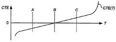
도 2는 본 발명에서 사용되는 유리(또는 유리세라믹)의 열팽창계수(CTE)의 온도의존성을 도시한 그래프,2 is a graph showing the temperature dependence of the coefficient of thermal expansion (CTE) of the glass (or glass ceramic) used in the present invention,
도 3은 본 발명에 따른 광학요소의 표면변형의 온도의존성을 도시한 그래프.3 is a graph showing the temperature dependence of the surface deformation of the optical element according to the present invention.
본 발명은,The present invention,
- 방사선의 투영빔을 공급하는 방사선시스템;A radiation system for supplying a projection beam of radiation;
- 원하는의 패턴에 따라 투영빔을 패터닝하는 역할을 하는 패터닝수단을 지지하는 지지구조체;A support structure for supporting patterning means, the patterning means serving to pattern the projection beam according to a desired pattern;
- 기판을 유지하는 기판테이블; 및A substrate table for holding a substrate; And
- 기판의 타겟부 위로 패터닝된 빔을 투영하는 투영시스템을 포함하여 이루어진 리소그래피 투영장치에 관한 것이다.A lithographic projection apparatus comprising a projection system for projecting a patterned beam onto a target portion of a substrate.
"패터닝수단(patterning means)"이라는 용어는 기판의 타겟부에 형성되어야 할 패턴에 대응하는 패터닝된 단면을 입사하는 방사선빔에 부여하도록 사용될 수 있는 수단을 의미하는 것으로서 폭넓게 해석되어야 하며, 본 명세서에서는 "광 밸브(light valve)"라는 용어로도 사용된다. 일반적으로, 상기 패턴은 집적회로 또는 기타 디바이스와 같이 타겟부에 형성될 디바이스 내의 특정 기능층에 해당할 것이다(이하 참조). 그러한 패터닝수단의 예로는 다음과 같은 것들이 포함된다.The term " patterning means " is to be broadly interpreted as meaning a means that can be used to impart a patterned cross section corresponding to a pattern to be formed on the target portion of the substrate to the incident radiation beam, and herein Also used as the term "light valve". In general, the pattern will correspond to a specific functional layer in the device to be formed in the target portion, such as an integrated circuit or other device (see below). Examples of such patterning means include the following.
- 마스크. 마스크의 개념은 리소그래피 분야에서 이미 잘 알려져 있고, 바이너리(binary)형, 교번 위상반전(alternating phase-shift)형 및 감쇠 위상반전형 마스크와 다양한 하이브리드 마스크 형식도 포함한다. 투영빔 내에 이러한 마스크가 놓이면, 마스크의 패턴에 따라 마스크에 입사되는 방사선의 선택적인 투과(투과 마스크의 경우) 또는 반사(반사 마스크의 경우)가 이루어진다. 마스크의 경우에, 그 지지구조체는 일반적으로 마스크테이블이며 이것은 입사하는 방사선빔 내의 원하는 위치에서 마스크를 잡아줄 수 있고 필요에 따라서는 빔에 대하여 이동될 수 있다.- Mask. The concept of masks is already well known in the lithography field and includes binary, alternating phase-shift and attenuated phase inverted masks and various hybrid mask types. When such a mask is placed in the projection beam, selective transmission (in the case of a transmission mask) or reflection (in the case of a reflection mask) of radiation incident on the mask is made according to the pattern of the mask. In the case of a mask, the support structure is generally a mask table, which can hold the mask at a desired position within the incident radiation beam and can be moved relative to the beam as needed.
- 프로그래머블 거울 어레이. 이러한 장치의 일례로는, 점탄성제어 층(viscoelastic control layer)과 반사면을 구비한 매트릭스-어드레서블 표면이 있다. 이러한 장치의 기본원리는, (예를 들어) 반사면의 어드레스된 영역(addressed area)에서는 입사광을 회절광으로 반사하는 한편, 어드레스되지 않은 영역에서는 입사광을 비회절광으로 반사하는 것이다. 적절한 필터를 사용하면, 반사된 빔 중에서 상기 비회절광을 필터링하여 회절광만 남게 할 수 있다. 이러한 방식으로 빔은 매트릭스-어드레서블 표면의 어드레싱 패턴에 따라 패터닝된다. 프로그래머블 거울 어레이의 대안적인 실시예는 국부화된 적절한 전기장을 가하거나 압전작동수단(piezoelectric actuation mean)을 채용하여 축을 중심으로 각각의 거울이 개별적으로 기울어질 수 있는 작은 거울들의 매트릭스 배치를 채용하는 것이다. 마찬가지로, 상기 거울은 매트릭스-어드레서블이며, 어드레스된 거울은 입사되는 방사선빔을 어드레스되지 않은 거울과는 다른 방향으로 반사한다. 이때 요구되는 매트릭스 어스레싱은 적절한 전자수단을 사용하여 수행될 수 있다. 상기에 서술된 두 가지 상황 모두에서, 패터닝수단은 1 이상의 프로그래머블 거울배열을 포함할 수 있다. 이러한 거울배열에 관한 더 많은 정보는, 예를 들어 본 명세서에서 참조되고 있는 미국특허 US 5,296,891호와 US 5,523,193호 및 PCT 특허출원 WO 98/38597호와 WO 98/33096호로부터 얻을 수 있다. 프로그래머블 거울 어레이의 경우, 상기 지지구조체는 예를 들어, 필요에 따라 고정되거나 움직일 수 있는 프레임 또는 테이블로써 구현될 수 있다.-Programmable mirror array. One example of such a device is a matrix-addressable surface with a viscoelastic control layer and a reflective surface. The basic principle of such a device is to reflect incident light as diffracted light in (eg) addressed areas of the reflective surface, while reflecting incident light as non-diffracted light in unaddressed areas. Using an appropriate filter, the undiffracted light can be filtered out of the reflected beam, leaving only the diffracted light behind. In this way the beam is patterned according to the addressing pattern of the matrix-addressable surface. An alternative embodiment of a programmable mirror array is to employ a matrix arrangement of small mirrors in which each mirror can be individually tilted about an axis by applying a localized appropriate electric field or employing piezoelectric actuation means. . Similarly, the mirror is matrix-addressable and the addressed mirror reflects the incident radiation beam in a different direction than the unaddressed mirror. The required matrix addressing can be performed using suitable electronic means. In both of the situations described above, the patterning means may comprise one or more programmable mirror arrays. More information regarding such mirror arrangements can be obtained, for example, from US Pat. Nos. 5,296,891 and 5,523,193 and PCT patent applications WO 98/38597 and WO 98/33096, which are hereby incorporated by reference. In the case of a programmable mirror array, the support structure may be embodied as a frame or table, for example, which may be fixed or movable as required.
- 프로그래머블 LCD 어레이. 이러한 구조의 일례는 본 명세서에서 참조되고 있는 미국특허 US 5,229,872호에 개시되어 있다. 상기와 마찬가지로, 이러한 경우 상기 지지구조체는 필요에 따라 고정되거나 움직일 수 있는 프레임 또는 테이블로써 구현될 수 있다.Programmable LCD Array. One example of such a structure is disclosed in US Pat. No. 5,229,872, which is incorporated herein by reference. As above, in this case the support structure may be embodied as a frame or table, which may be fixed or movable as required.
설명을 간단히 하기 위하여, 본 명세서의 나머지 부분 중 어느 곳에서는 그 자체가 마스크 및 마스크테이블을 포함하는 예시적인 용어로서 지칭될 수도 있다. 하지만, 그러한 예시에서 논의된 일반적인 원리는 상술한 바와 같은 패터닝수단의 광의의 개념으로 이해되어야 한다.For simplicity of explanation, any of the remainder of this specification may, by itself, be referred to as exemplary terms including masks and mask tables. However, the general principles discussed in such examples should be understood as the broad concept of the patterning means as described above.
예를 들어, 리소그래피 투영장치는 집적회로(IC)의 제조에 사용될 수 있다. 이러한 경우, 상기 패터닝수단은 IC의 개별층에 해당하는 회로패턴을 생성할 수 있으며, 상기 패턴은 한 층의 방사선감응재(레지스트)로 코팅된 기판(실리콘 웨이퍼)상의 타겟부(예를 들면, 1이상의 다이로 구성되는)에 이미징될 수 있다. 일반적으로 한장의 웨이퍼에는 인접하여 있는 여러 개의 타겟부로 구성된 전체적인 네트워크를 포함하며, 이들 타겟부는 투영시스템을 통하여 한번에 하나씩 연속적으로 조사된다. 현재 통용되는 장치에서, 마스크테이블상의 마스크에 의한 패터닝을 채택하는 데에는, 두 가지 서로 다른 형식의 기계로 구분될 수 있다. 한 가지 형태의 리소그래피 투영장치에서는 타겟부상에 전체 마스크패턴을 한번에 노광함으로써 각 타겟부가 조사되는데, 이러한 장치를 통상 웨이퍼 스테퍼(wafer stepper)라고 한다. 통상, 스텝-앤드-스캔 장치(step-and-scan apparatus)라고 불리워지는 대체장치에서는 투영빔하에서 주어진 기준방향("스캐닝" 방향)으로 마스크 패턴을 점진적으로 스캐닝하는 한편, 이 방향과 같은 방향 또는 반대 방향으로 기판을 동기화시켜 스캐닝함으로써 각 타겟부가 조사된다. 일반적으로 투영시스템은 배율인자 M(일반적으로 <1)을 가지므로 기판테이블이 스캐닝되는 속도 V는 마스크테이블이 스캐닝되는 속도의 인자 M배가 된다. 여기에 서술된 리소그래피장치와 관련된 보다 상세한 정보는 예를 들어, US 6,046,792호로부터 얻을 수 있으며 본 명세서에서도 참조자료로 채용된다.Lithographic projection apparatus can be used, for example, in the manufacture of integrated circuits (ICs). In this case, the patterning means can generate a circuit pattern corresponding to an individual layer of the IC, the pattern being a target portion (for example, on a substrate (silicon wafer) coated with a layer of radiation sensitive material (resist) Imaged with one or more dies). In general, a single wafer includes an entire network of adjacent target portions, which are sequentially irradiated one at a time through the projection system. In today's devices, the adoption of patterning by masks on a mask table can be divided into two different types of machines. In one type of lithographic projection apparatus, each target portion is irradiated by exposing the entire mask pattern onto the target portion at once. Such an apparatus is commonly referred to as a wafer stepper. An alternative apparatus, commonly referred to as a step-and-scan apparatus, progressively scans the mask pattern under a projection beam in a given reference direction ("scanning" direction), while in the same direction as this direction or Each target portion is irradiated by synchronously scanning the substrate in the opposite direction. Since the projection system generally has a magnification factor M (generally <1), the speed V at which the substrate table is scanned is a factor M times that at which the mask table is scanned. More detailed information relating to the lithographic apparatus described herein can be obtained, for example, from US Pat. No. 6,046,792, which is also incorporated herein by reference.
리소그래피 투영장치를 사용하는 제조공정에서, (예를 들어, 마스크의) 패턴은 방사선감응재(레지스트)의 층이 최소한의 부분에라도 도포된 기판상에 이미징된다. 이 이미징단계에 앞서, 기판은 전처리(priming), 레지스트도포 및 소프트 베이크와 같은 여러가지 과정을 거칠 수 있다. 노광 후에는, 노광후 베이크(PEB), 현상, 하드 베이크 및 이미징된 피쳐의 측정/검사와 같은 또 다른 과정을 거치게 된다. 이러한 일련의 과정은, 예를 들어 IC 디바이스의 개별층을 패터닝하는 기초로서 사용된다. 그런 다음 이렇게 패터닝된 층은 에칭, 이온주입(도핑), 금속화, 산화, 화학-기계적 폴리싱 등과 같은, 모두가 개별층을 마무르도록 하는 여러 공정을 거친다. 여러 개의 층이 요구된다면, 새로운 층마다 전체공정 또는 그것의 변형된 공정이 반복되어져야만 할 것이다. 그 결과로, 기판(웨이퍼)상에는 디바이스의 배열이 존재하게 될 것이다. 이들 디바이스는 다이싱 또는 소잉 등의 기술에 의하여 서로 분리되고, 이들 각각의 디바이스는 캐리어에 장착되고 핀 등에 접속될 수 있다. 이와 같은 공정에 관한 추가 정보는, 예를 들어, 본 명세서에서 참조자료로 채용되고 있는 "Microchip Fabrication: A Practical Guide to Semiconductor Processing" (3판, Peter van Zant 저, McGraw Hill출판사, 1997년, ISBN 0-07-067250-4)으로부터 얻을 수 있다.In a manufacturing process using a lithographic projection apparatus, a pattern (eg of a mask) is imaged onto a substrate on which a layer of radiation sensitive material (resist) is applied even to a minimum portion. Prior to this imaging step, the substrate may be subjected to various processes such as priming, resist coating and soft bake. After exposure, there is another process such as post-exposure bake (PEB), development, hard bake and measurement / inspection of the imaged features. This series of procedures is used, for example, as the basis for patterning individual layers of IC devices. The patterned layer is then subjected to several processes, such as etching, ion implantation (doping), metallization, oxidation, chemical-mechanical polishing, etc., all to finish the individual layer. If several layers are required, the whole process or its modified process will have to be repeated for each new layer. As a result, there will be an arrangement of devices on the substrate (wafer). These devices are separated from each other by a technique such as dicing or sawing, and each of these devices can be mounted to a carrier and connected to a pin or the like. Further information on such a process can be found in, for example, "Microchip Fabrication: A Practical Guide to Semiconductor Processing" (3rd edition, Peter van Zant, McGraw Hill, 1997, ISBN) 0-07-067250-4).
설명을 간단히 하기 위하여, 상기 투영시스템은 이후에 "렌즈"라고 언급될 수 있다. 하지만 이 용어는 예를 들어, 굴절광학기, 반사광학기 및 카타디옵트릭 (catadioptric) 시스템을 포함한 다양한 형태의 투영시스템을 포괄하는 것으로서 폭넓게 해석되어야 한다. 또한 상기 방사선시스템은 방사선 투영빔의 지향, 성형 또는 제어하기 위한 임의의 이들 설계방식에 따라 동작하는 구성요소를 포함할 수 있고, 이후의 설명에서는 이러한 구성요소들을 집합적으로 또는 개별적으로 "렌즈"라고 언급할 것이다. 더 나아가, 상기 리소그래피장치는 2이상의 기판테이블(및/또는 2 이상의 마스크테이블)을 구비하는 형태가 될 수도 있다. 이러한 "다수 스테이지" 장치에서는 추가 테이블이 병행으로 사용될 수 있으며, 1이상의 테이블이 노광에서 사용되고 있는 동안 1이상의 다른 테이블에서는 준비작업 단계가 수행될 수 있다. 예를 들어 US 5,969,441호 및 WO 98/40791호에는 듀얼스테이지 리소그래피장치가 개시되어 있으며, 본 명세서에서도 인용 참조되고 있다.For simplicity of explanation, the projection system may hereinafter be referred to as a "lens." However, the term should be broadly interpreted as encompassing various types of projection systems, including, for example, refractive optics, reflective optics and catadioptric systems. The radiation system may also include components that operate according to any of these design schemes for directing, shaping or controlling the projection beam of radiation, and in the following description these components are collectively or individually "lens". Will be mentioned. Furthermore, the lithographic apparatus may be of a type having two or more substrate tables (and / or two or more mask tables). In such " multiple stage " devices the additional tables can be used in parallel, and preparatory steps can be carried out on one or more tables while one or more other tables are being used for exposure. For example, US Pat. No. 5,969,441 and WO 98/40791 disclose dual stage lithographic apparatus, which are also incorporated herein by reference.
보다 더 작은 피처를 이미징하기 위해서는 현재의 통용되는 리소그래피장치에서 사용되는 193 또는 157nm의 파장을 가진 UV 대신에 노광 방사선으로서 5 내지 20nm 범위의 파장을 가진 EUV 방사선을 사용할 것이 제안되고 있다. EUV 방사선을 위한 방사선시스템 및/또는 투영시스템내 광학요소용 굴절렌즈를 형성할 수 있는 재료가 알려져 있지 않아서, EUV 리소그래피장치의 방사선 및 투영시스템은 거울, 보통은 다층 거울을 사용하여 만들어져야 한다. 이미징될 이미지의 품질은 거울의 표면 변형(모양 에러)에 극히 민감하며 투영시스템의 그것에 특히 그러하다. 온도변화로 생기는 표면 변형을 막기 위해서, 거울은 원하는 모양을 가진 기판상에 다층 스택을 퇴적함으로써 형성되고 열팽창계수(CTE)가 극히 낮거나 0인 재료로 이루어진다. 이러한 다양한 재료는 여러 공급자들로부터 시중에서 구할 수 있다. 한가지는 ZerodurTM으로서 이것은 원하는 낮은 CTE를 제공하도록 여러가지 첨가물과 함께 이루어진 유리 세라믹이다. 이들 재료는 매우 낮은 CTE를 갖기는 하지만, 어떤 온도에서만 CTE가 정확히 0이어서 어느정도의 열팽창 및 열수축이 발생하여 표면 변형과 이미지 품질의 손실을 유발한다.In order to image smaller features, it is proposed to use EUV radiation having a wavelength in the range of 5 to 20 nm as exposure radiation instead of UV having a wavelength of 193 or 157 nm used in current lithography apparatus. The radiation and projection system of the EUV lithographic apparatus should be made using mirrors, usually multilayer mirrors, since no material is known which can form refractive systems for EUV radiation and / or refractive lenses for optical elements in the projection system. The quality of the image to be imaged is extremely sensitive to the surface deformation (shape error) of the mirror and especially so of that of the projection system. To prevent surface deformation caused by temperature changes, the mirror is formed by depositing a multilayer stack on a substrate having the desired shape and made of a material with an extremely low or zero coefficient of thermal expansion (CTE). These various materials are available commercially from various suppliers. One is Zerodur™, which is a glass ceramic made with various additives to provide the desired low CTE. Although these materials have very low CTEs, only at certain temperatures the CTEs are exactly zero, causing some thermal expansion and thermal contraction, leading to surface deformation and loss of image quality.
본 발명의 목적은 방사선 및/또는 투영시스템내 광학요소의 열이 이미징 품질에 미치는 영향이 더욱 감소되거나 혹은 제거되는 리소그래피 투영장치를 제공하는 것이다.It is an object of the present invention to provide a lithographic projection apparatus in which the influence of radiation and / or heat of optical elements in the projection system on the imaging quality is further reduced or eliminated.
본 발명에 따라, 서두에 언급된 리소그래피장치로서, 상기 장치내의 사용시 열 부하를 받는 하나 이상의 구성요소가 상기 구성요소의 제작온도와 평균 작동온도 사이의 온도에서 영교차(zero-crossing) 열팽창계수를 가진 낮은 CTE 재료로 이루어지는 것을 특징으로 하는 리소그래피장치를 통하여 상기 목적 및 기타 목적이 성취된다.According to the invention, the lithographic apparatus mentioned at the outset is characterized in that at least one component subjected to a heat load in use in the apparatus has a zero-crossing coefficient of thermal expansion at a temperature between the fabrication temperature and the average operating temperature of the component. This and other objects are achieved through a lithographic apparatus characterized in that it is made of a low CTE material.
구성요소의 제작온도와 평균 작동온도 사이에서 CTE 영교차 온도를 가지는 재료를 사용하여 구성요소를 구성하면, 동작시 구성요소의 열 변형이 최소화되거나 제거된다. 일반적으로 CTE는 구성요소의 온도가 그것의 제작온도로부터 작동온도로 변화함에 따라 영교차 온도 아래에서는 음이 되고 그 위에서는 양이 될 것이기 때문에, 상기 구성요소는 초기에는 형체가 바뀌지만 이들 변형은 영교차 온도의 다른 쪽에서는 반전될 것이다.The construction of the component using a material having a CTE zero crossing temperature between the component's fabrication temperature and its average operating temperature minimizes or eliminates thermal deformation of the component during operation. In general, since the CTE will be negative below zero crossing temperature and positive above it as the temperature of the component changes from its fabrication temperature to its operating temperature, the component will initially change shape, but these variations On the other side of the zero crossing temperature it will be reversed.
영교차의 이상적인 온도는 영교차 영역에서 온도의 함수인 CTE의 모습에 따라 다를 것이다. CTE가 그 영역내 온도에 선형으로 의존한다면, 제작온도와 평균 작동온도 사이의 정확히 중간 지점에서 CTE 영교차 재료가 사용되어야 한다. 일반적으로, 제작온도, 영교차 온도 및 평균 작동온도는 제작온도와 평균 작동온도 사이의 온도의존성 CTE의 적분값이 0이거나 가능한 0에 가깝도록 되어야 한다.The ideal temperature of zero crossing will depend on the appearance of the CTE as a function of temperature in the zero crossing region. If the CTE is linearly dependent on temperature in that area, the CTE zero crossing material should be used at exactly halfway between the fabrication temperature and the average operating temperature. In general, the fabrication temperature, the zero crossing temperature and the average operating temperature should be such that the integral value of the temperature dependent CTE between the fabrication temperature and the average operating temperature is zero or as close to zero as possible.
사용되는 재료가 유리 혹은 ZerodurTM와 같은 유리세라믹인 경우에, CTE 영교차 온도는 첨가제 및/또는 제작 과정의 적절한 제어에 따라 원하는 대로 선택될 수 있다. 필요하다면, 원하는의 CTE 영교차 온도의 유리(또는 유리세라믹)의 배치(batch)는 시행착오를 거쳐 제작될 수 있다. 장치의 평균 작동온도는 다른 고려하에서 결정된다 하더라도 제작온도는 일정한 또는 한정된 가변성만을 가진 CTE 영교차 온도를 가진 특정 유리(또는 유리세라믹)의 사용이 가능하도록 조정될 수 있다.If the material used is glass or glass ceramics such as Zerodur™ , the CTE zero crossover temperature can be selected as desired under appropriate control of the additives and / or fabrication process. If desired, a batch of glass (or glass ceramics) of the desired CTE zero cross temperature can be produced by trial and error. Although the average operating temperature of the device may be determined under other considerations, the fabrication temperature may be adjusted to enable the use of specific glass (or glass ceramics) with CTE zero crossing temperatures with only constant or limited variability.
본 발명은 리소그래피장치내의 어떠한 구성요소에소 적용될 수 있지만, 투영빔의 경로에 있는 광학요소, 특히 EUV 리소그래피장치내의 거울, 특히 표면변형이 이미징품질에 가장 큰 영향을 미치는 투영시스템의 거울 및 투영빔 세기가 가장 커서 더 큰 온도 변화를 유발하는 조명시스템의 시작 부분에 있는 거울에 적용될 때 특히 유리하다. 본 발명은 또한 열 부하가 집중되어서 역시 더 큰 온도변화를 유발하는 작은 거울에 특히 적용 가능하다. 다층 거울에 대하여, 기판만을 위하여, 또 다층 스택이 아닌 경우에도 낮은 CTE 재료로 만들어질 수 있다는 것을 알 수 있다.Although the invention can be applied to any component in the lithographic apparatus, optical elements in the path of the projection beam, in particular mirrors in the EUV lithographic apparatus, in particular mirrors and projection beams of the projection system, in which surface deformation has the greatest influence on the imaging quality. This is particularly advantageous when applied to mirrors at the beginning of the lighting system, which have the greatest intensity and cause greater temperature changes. The invention is also particularly applicable to small mirrors in which the heat load is concentrated, which also causes a greater temperature change. It can be seen that for a multilayer mirror, it can be made of low CTE material for the substrate only and not in the multilayer stack.
일반적으로는 일관성의 측면에서 리소그래피장치내 투영빔에 영향을 미치는 광학요소 모두를 동일한 배치의 재료로 만들어서, 상이한 광학요소의 작동온도가 다른 경우에 영교차 온도는 한 가지 요소에 대하여만 이상적일 수 있게 하는 것이 바람직하다. 그러한 경우에, 영교차 온도는 가장 큰 온도 부하를 가진 거울, 일반적으로 제1거울에 대하여 이상적으로 되도록 선택되는 것이 바람직하다.Generally, in terms of consistency, all optical elements that affect the projection beam in the lithographic apparatus are made of the same batch of material, so that the zero crossing temperature may be ideal for only one element when the operating temperatures of the different optical elements are different. It is desirable to have. In such a case, the zero crossing temperature is preferably chosen to be ideal for the mirror with the largest temperature load, generally the first mirror.
본 발명의 다른 실시형태에 따르면,According to another embodiment of the present invention,
- 적어도 부분적으로는 방사선 감응재의 층으로 덮인 기판을 제공하는 단계;Providing a substrate at least partially covered with a layer of radiation sensitive material;
- 방사선시스템을 사용하여 방사선의 투영빔을 제공하는 단계;Providing a projection beam of radiation using a radiation system;
- 패터닝수단을 사용하여 투영빔의 단면에 패턴을 부여하는 단계;Imparting a pattern to the cross section of the projection beam using patterning means;
- 방사선감응재층의 타겟부상으로 방사선의 패터닝된 빔을 투영하는 단계를 포함하는 디바이스 제조방법에 있어서,A device manufacturing method comprising projecting a patterned beam of radiation onto a target portion of a layer of radiation sensitive material,
상기 장치내의 사용시 열 부하를 받는 하나 이상의 구성요소는 평균 작동온도를 가지며 상기 구성요소의 제작온도와 상기 평균 작동온도 사이의 온도에서 영교차 열팽창계수를 가진 낮은 CTE 재료로 이루어지는 것을 특징으로 하는 디바이스 제조방법이 제공된다.At least one component subjected to heat load during use in the device comprises a low CTE material having an average operating temperature and having a low cross-coefficient of thermal expansion coefficient at temperatures between the fabrication temperature of the component and the average operating temperature. A method is provided.
본 발명의 또 다른 실시형태에 따르면, 사용시 열 부하를 받으며 평균 작동온도에서 작동되는 광학요소를 제작하는 방법으로서,According to another embodiment of the present invention, there is provided a method of manufacturing an optical element which is operated at an average operating temperature under heat load in use,
제1온도에서 열팽창계수가 0인 낮은 CTE 재료를 선택하는 단계; 및Selecting a low CTE material having a coefficient of thermal expansion of zero at a first temperature; And
제2온도에서 상기 낮은 CTE 재료를 사용하여 적어도 상기 광학요소를 제작하는 단계를 포함하며,Fabricating at least the optical element using the low CTE material at a second temperature,
상기 작동온도에서 상기 광학요소의 표면변형을 최소화하도록, 상기 제1온도는 상기 제2온도와 상기 평균 작동온도의 사이에 있는 것을 특징으로 하는 광학요 소를 제작하는 방법이 제공된다.In order to minimize the surface deformation of the optical element at the operating temperature, the first temperature is provided between the second temperature and the average operating temperature is provided.
본 명세서에서는 IC의 제조에 있어서의 본 발명에 따른 장치의 사용례에 대하여 언급하였으나, 이러한 장치가 다른 여러 가능한 응용례를 가지고 있음이 명백히 이해되어야 할 것이다. 예를 들어, 상기 장치는 집적 광학시스템, 자기영역메모리용 유도 및 검출패턴, 액정표시패널, 박막자기헤드 등의 제조에도 이용될 수 있다. 당업자라면, 이러한 대안적인 적용례와 관련하여, 본 명세서에서 사용된 "레티클", "웨이퍼" 또는, "다이"와 같은 용어가 각각 "마스크", "기판" 및 "타겟부" 등과 같은 좀 더 일반적인 용어로 대체되고 있음을 이해할 수 있다.Although reference is made herein to the use of the device according to the invention in the manufacture of ICs, it will be clearly understood that such devices have many other possible applications. For example, the apparatus may be used for manufacturing integrated optical systems, induction and detection patterns for magnetic region memories, liquid crystal display panels, thin film magnetic heads, and the like. As those skilled in the art relate to these alternative applications, the terms "reticle", "wafer", or "die" as used herein are more generic, such as "mask", "substrate", and "target", respectively. It will be understood that the term is being replaced with.
본 명세서에서, "방사선" 및 "빔"이란 용어는 (예를 들어, 파장이 365, 248, 193, 157 또는 126㎚ 인)자외선 및 EUV(극자외선, 예를 들어 파장이 5 내지 20㎚ 범위인)를 포함한 모든 형태의 전자기방사선뿐만 아니라 이온빔이나 전자빔과 같은 입자빔까지도 포괄하여 사용된다.As used herein, the terms "radiation" and "beam" refer to ultraviolet (eg, wavelengths 365, 248, 193, 157, or 126 nm) and EUV (extreme ultraviolet, eg, wavelengths ranging from 5 to 20 nm). All types of electromagnetic radiation, including phosphorus), as well as particle beams such as ion beams and electron beams are used.
이하, 첨부된 개략적인 도면을 참조로 단지 예시의 방식으로 본 발명의 실시예를 서술한다.DESCRIPTION OF THE EMBODIMENTS Hereinafter, embodiments of the present invention will be described by way of example only with reference to the accompanying schematic drawings.
제1실시예First embodiment
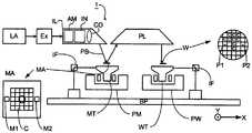
도 1은 본 발명의 특정한 실시예에 따른 리소그래피 투영장치를 개략적으로 도시한다. 상기 장치는,1 schematically depicts a lithographic projection apparatus according to a particular embodiment of the invention. The device,
- 방사선(예를 들어, EUV 방사선)의 투영빔(PB)을 공급하는 방사선시스템 (Ex, IL)(특별히 여기에서는 방사선시스템이 방사원(LA)도 포함한다);A radiation system Ex, IL for supplying a projection beam PB of radiation (eg EUV radiation), in particular where the radiation system also includes a radiation source LA;
- 마스크(MA)(예를 들어, 레티클)를 유지하는 마스크 홀더가 마련된, 아이템 (PL)에 대하여 마스크를 정확히 위치시키는 제1위치설정수단(PM)에 연결된 제1대물테이블(마스크테이블)(MT);A first object table (mask table) connected to first positioning means PM for accurately positioning the mask with respect to the item PL, provided with a mask holder for holding the mask MA (e.g. a reticle) ( MT);
- 기판(W)(예를 들어, 레지스트 코팅된 실리콘 웨이퍼)을 유지하는 기판 홀더가 마련된, 아이템(PL)에 대하여 기판을 정확히 위치시키는 제2위치설정수단 (PW)에 연결된 제2대물테이블(기판테이블)(WT); 및A second object table connected to a second positioning means PW for accurately positioning the substrate with respect to the item PL, provided with a substrate holder for holding the substrate W (e.g., a resist coated silicon wafer). Substrate table) WT; And
- 기판(W)의 타겟부(C)(1이상의 다이를 포함)에 마스크(MA)의 조사된 부분을 이미징하는 투영시스템("렌즈")(PL)(예를 들어, 다층 거울의 그룹)을 포함하여 이루어진다.A projection system (" lens ") PL (e.g. a group of multilayer mirrors) for imaging the irradiated portion of the mask MA on the target portion C (including one or more dies) of the substrate W; It is made, including.
도시된 바와 같이, 상기 장치는 (반사마스크를 구비한) 반사형(reflective type)이다. 하지만, 일반적으로는, 예를 들어 (투과마스크를 구비한) 투과형일 수도 있다. 대안으로, 상기 장치는 위에서 언급한 바와 같은 형태의 프로그래머블 거울 어레이와 같은 그 밖의 다른 종류의 패터닝수단을 채용할 수도 있다.As shown, the device is of reflective type (with a reflective mask). In general, however, it may also be a transmission type (with a transmission mask), for example. Alternatively, the apparatus may employ other kinds of patterning means, such as a programmable mirror array of the type mentioned above.
방사원(LA)(예를 들어, 레이저생성 플라즈마원 혹은 방전 플라즈마원)은 방사선의 빔을 생성한다. 상기 빔은 곧바로 조명시스템(일루미네이터)(IL)에 들어 가거나, 예를 들어 빔 익스펜더(Ex)와 같은 컨디셔닝 수단을 거친 다음에 조명시스템으로 들어간다. 상기 일루미네이터(IL)는 빔내의 세기 분포의 외반경 및/또는 내반경 크기(통상 각각 외측-σ 및 내측-σ라 함)를 설정하는 조정수단(AM)을 포함하여 이루어진다. 또한 그것은 일반적으로 인티그레이터(IN) 및 콘덴서(CO)와 같은 그 밖의 다른 다양한 구성요소들을 포함하고 있다. 이러한 방식으로, 마스크(MA)에 도달하는 빔(PB)은 그 단면에 원하는 균일성과 세기 분포를 갖게 된다.The radiation source LA (eg, a laser generating plasma source or a discharge plasma source) generates a beam of radiation. The beam directly enters the illumination system (illuminator) IL or passes through conditioning means such as, for example, beam expander Ex and then into the illumination system. The illuminator IL comprises adjusting means AM for setting the outer and / or inner radial extent (commonly referred to as -outer and -inner, respectively) of the intensity distribution in the beam. It also generally contains other various components such as integrator IN and capacitor CO. In this way, the beam PB reaching the mask MA has the desired uniformity and intensity distribution in its cross section.
도 1과 관련하여, 상기 방사원(LA)은 리소그패피 투영장치의 하우징내에 놓이지만(흔히 예를 들어, 방사원(LA)이 수은 램프인 경우에서처럼), 그것이 리소그래피 투영장치로부터 멀리 떨어져 있어서 그것이 만들어 낸 방사선빔이 (가령, 적절한 지향 거울에 의해) 장치 내부로 들어오게 할 수도 있다. 후자의 시나리오는 방사원(LA)이 흔히 엑시머레이저인 때의 경우이다. 본 발명과 청구 범위는 이들 시나리오를 모두 포함하고 있다.1, the radiation source LA is placed in the housing of the lithographic package projector (often as in the case where the radiation source LA is a mercury lamp), but it is far from the lithographic projection apparatus so that it is made It is also possible for the emitted radiation beam to enter the device (eg by means of a suitable directional mirror). The latter scenario is when the radiation source LA is often an excimer laser. The present invention and claims encompass both of these scenarios.
이후, 상기 빔(PB)은 마스크테이블(MT)상에 잡혀있는 마스크(MA)를 통과한다. 마스크(MA)를 지난 빔(PB)은 렌즈(PL)를 통과하여 기판(W)의 타겟부(C)위에 빔(PB)을 포커스한다. 제2위치설정수단(및 간섭계측정수단(IF))에 의하여, 기판테이블(WT)은, 예를 들어 빔(PB)의 경로내에 상이한 타겟부(C)를 위치시키도록 정확하게 이동될 수 있다. 이와 유사하게, 제1위치설정수단은 예를 들어, 마스크 라이브러리로부터 마스크(MA)를 기계적으로 회수한 후에, 또는 스캔하는 동안, 빔(PB)의 경로에 대하여 마스크(MA)를 정확히 위치시키도록 사용될 수 있다. 일반적으로 대물테이블(MT, WT)의 이동은, 도 1에 명확히 도시되지는 않았지만, 긴행정모듈 (long stroke module)(개략 위치설정) 및 짧은행정모듈(미세 위치설정)의 도움을 받아 실현될 것이다. 하지만, (스텝-앤드-스캔장치와는 대조적으로) 웨이퍼스테퍼의 경우에는 마스크테이블(MT)이 짧은행정모듈에만 연결될 수도 있고 고정될 수도 있다.The beam PB subsequently intercepts the mask MA, which is held on a mask table MT. The beam PB passing through the mask MA passes through the lens PL to focus the beam PB on the target portion C of the substrate W. By means of the second positioning means (and interferometric measuring means IF), the substrate table WT can be accurately moved to position different target portions C in the path of the beam PB, for example. Similarly, the first positioning means is adapted to accurately position the mask MA with respect to the path of the beam PB, for example after mechanically withdrawing the mask MA from the mask library or during scanning. Can be used. In general, the movement of the objective tables MT, WT, although not clearly shown in FIG. 1, can be realized with the help of a long stroke module (coarse positioning) and a short stroke module (fine positioning). will be. However, in the case of a wafer stepper (as opposed to a step-and-scan apparatus), the mask table MT may be connected or fixed only to a short stroke module.
상술한 장치는 다음의 두 가지 상이한 모드로 사용될 수 있다.The apparatus described above can be used in two different modes:
1. 스텝 모드에서는, 마스크테이블(MT)은 기본적으로 정지상태로 유지되며, 전체 마스크 이미지는 한번에(즉, 단일 "섬광"으로) 타겟부(C)에 투영된다. 이후 기판테이블(WT)이 x 및/또는 y 방향으로 쉬프트되어 다른 타겟부(C)가 빔(PB)에 의하여 조사될 수 있다.1. In the step mode, the mask table MT is basically kept stationary, and the entire mask image is projected onto the target portion C at once (ie, in a single "flash"). Subsequently, the substrate table WT is shifted in the x and / or y directions so that another target portion C may be irradiated by the beam PB.
2. 스캔 모드에서는, 주어진 타겟부(C)가 단일 "섬광"으로 노광되지 않는 것을 제외하고는 기본적으로 동일한 시나리오가 적용된다. 그 대신에, 마스크테이블(MT)이v의 속도로 주어진 방향(소위 "스캔방향", 예를 들어 y 방향)으로 이동 가능해서, 투영빔(PB)이 마스크 이미지의 모든 부분을 스캐닝하도록 되고, 이와 함께 기판테이블(WT)은 속도V=Mv로, 동일한 방향 또는 그 반대 방향으로 동시에 이동하는 데, 이 때M은 렌즈(PL)의 배율(통상M=1/4 또는M=1/5)이다. 이러한 방식으로, 해상도를 떨어뜨리지 않고도 비교적 넓은 타겟부(C)가 노광될 수 있다.2. In scan mode, basically the same scenario applies, except that a given target portion C is not exposed in a single "flash". Instead, the mask table MT is movable in a given direction (so-called " scan direction ", for example y direction) at a velocity ofv so that the projection beam PB is to scan all parts of the mask image, In addition, the substrate table WT simultaneously moves in the same direction or the opposite direction at the speedV =Mv , whereM is the magnification of the lens PL (usuallyM = 1/4 orM = 1/5). to be. In this way, a relatively wide target portion C can be exposed without degrading the resolution.
도 2는 리소그래피장치의 조명 및 투영시스템내 다층 거울의 기판을 만드는 데 사용될 수 있는 ZerodurTM과 같은 낮은 CTE 유리세라믹 혹은 ULETM과 같은 유리의 열팽창계수의 온도의존성을 도시한다. 온도 T의 함수인 열팽창계수로서, 곡선 CET(T)는 온도 B에서 영교차되고 B의 양쪽 온도 범위에 대하여 실질적으로 선형이다. 본 발명에 따라, 광학요소는 온도 A에서 제작되고 온도 C에서 작동되어, CTE(T)가 실질적으로 선형이고 B가 A와 C의 사이에 있는 온도 범위내에 A와 C가 있으므로 다음과 같다.2 shows the temperature dependence of the coefficient of thermal expansion of a glass such as ULE™ or a low CTE glass ceramic such as Zerodur™ which can be used to make a substrate of a multilayer mirror in the illumination and projection system of a lithographic apparatus. As a coefficient of thermal expansion as a function of temperature T, curve CET (T) is zero crossing at temperature B and is substantially linear over both temperature ranges of B. According to the invention, the optical element is fabricated at temperature A and operated at temperature C, so that A and C are within the temperature range where CTE (T) is substantially linear and B is between A and C as follows.
바람직하게는, 영교차 온도 B가 제작온도 A와 평균 작동온도 C의 중간에 있으므로 다음과 같다.Preferably, the zero crossing temperature B is in the middle of the production temperature A and the average operating temperature C as follows.

더 일반적인 경우에, CTE(T)가 A 내지 C의 범위에서 선형이지 않으면, 유리 (또는 유리세라믹)의 제작온도 및/또는 평균 작동온도는 다음과 같이 되도록 선택되어야 한다.In a more general case, if CTE (T) is not linear in the range of A to C, the fabrication temperature and / or average operating temperature of the glass (or glass ceramic) should be chosen to be as follows.

상기 기준을 만족한다면, 평균 작동온도에서 거울의 표면변형은 실질적으로 0일 것이다. 이것은 온도 T의 함수인 표면변형 d를 도시한 도 3으로부터 알 수 있다. 본 예시에서, A가 C보다 작고 CTE(T)가 B 아래에서는 음의 값을 가지는 경우, 온도가 A에서 B로 상승함에 따라 거울의 초기 수축은 온도가 B 위로 계속 상승하면서 반전된다.If the above criteria are met, the surface deformation of the mirror at the average operating temperature will be substantially zero. This can be seen from FIG. 3 which shows the surface strain d as a function of temperature T. In this example, when A is less than C and CTE (T) has a negative value below B, the initial shrinkage of the mirror is reversed as the temperature continues to rise above B as the temperature rises from A to B.
예로서, 제작온도가 22℃이고 평균 작동온도가 대략 30℃라면, 26℃의 영교차 CTE를 가진 유리(또는 유리세라믹)가 선택될 것이다.As an example, if the fabrication temperature is 22 ° C. and the average operating temperature is approximately 30 ° C., a glass (or glass ceramic) with a zero crossing CTE of 26 ° C. will be selected.
당업자라면, 리소그래피장치에 사용되는 것과 같은 고정밀 광학요소는 보통 매우 일정한 온도를 유지한 채로 그것의 최종 형태로 그라인드된다는 것을 잘 알 것이다. 하지만, 다른 온도에서 제작하는 단계의 경우에 본 발명의 목적에 관련되 는 온도는 최종 폴리싱 및 모양검사 단계의 온도이다.Those skilled in the art will appreciate that high precision optical elements, such as those used in lithographic apparatus, are usually ground in their final form while maintaining a very constant temperature. However, in the case of fabrication steps at other temperatures, the temperature relevant to the object of the present invention is the temperature of the final polishing and shape inspection steps.
이상 본 발명의 특정 실시예를 서술하였지만, 본 발명이 서술된 바와 다르게도 실시될 수 있음을 알 수 있다. 상기 내용은 본 발명을 제한하려는 것이 아니다.While specific embodiments of the invention have been described above, it will be appreciated that the invention may be practiced otherwise than as described. The foregoing is not intended to limit the invention.
이상과 같이, 본 발명에 따르면 방사선 및/또는 투영시스템내 광학요소의 열이 이미징 품질에 미치는 영향이 더욱 감소되거나 혹은 제거되는 리소그래피 투영장치가 제공된다.As described above, according to the present invention, there is provided a lithographic projection apparatus in which the effect of heat of the radiation and / or optical elements in the projection system is further reduced or eliminated.
Claims (9)
Translated fromKoreanApplications Claiming Priority (2)
| Application Number | Priority Date | Filing Date | Title |
|---|---|---|---|
| EP01310155.5 | 2001-12-04 | ||
| EP01310155 | 2001-12-04 |
Publications (2)
| Publication Number | Publication Date |
|---|---|
| KR20030076190A KR20030076190A (en) | 2003-09-26 |
| KR100588126B1true KR100588126B1 (en) | 2006-06-09 |
Family
ID=8182514
Family Applications (1)
| Application Number | Title | Priority Date | Filing Date |
|---|---|---|---|
| KR1020020075855AExpired - Fee RelatedKR100588126B1 (en) | 2001-12-04 | 2002-12-02 | Lithographic apparatus, device manufacturing method and optical element manufacturing method |
Country Status (6)
| Country | Link |
|---|---|
| US (2) | US6747730B2 (en) |
| JP (1) | JP3588095B2 (en) |
| KR (1) | KR100588126B1 (en) |
| CN (1) | CN1282039C (en) |
| SG (1) | SG103376A1 (en) |
| TW (1) | TWI260469B (en) |
Families Citing this family (11)
| Publication number | Priority date | Publication date | Assignee | Title |
|---|---|---|---|---|
| US7428037B2 (en)* | 2002-07-24 | 2008-09-23 | Carl Zeiss Smt Ag | Optical component that includes a material having a thermal longitudinal expansion with a zero crossing |
| JP4817844B2 (en)* | 2003-09-27 | 2011-11-16 | カール・ツァイス・エスエムティー・ゲーエムベーハー | EUV projection lens having a mirror made of a material having a different sign of inclination with respect to a temperature rise in accordance with a thermal expansion coefficient around a zero transition temperature |
| JP4537087B2 (en)* | 2004-02-12 | 2010-09-01 | キヤノン株式会社 | Exposure apparatus and device manufacturing method |
| US7295284B2 (en)* | 2004-02-27 | 2007-11-13 | Canon Kk | Optical system, exposure apparatus using the same and device manufacturing method |
| WO2007010011A2 (en)* | 2005-07-19 | 2007-01-25 | Carl Zeiss Smt Ag | Optical element module |
| DE102008002403A1 (en)* | 2008-06-12 | 2009-12-17 | Carl Zeiss Smt Ag | Method for producing a multilayer coating, optical element and optical arrangement |
| EP2221669A3 (en)* | 2009-02-19 | 2011-02-09 | ASML Netherlands B.V. | A lithographic apparatus, a method of controlling the apparatus and a device manufacturing method |
| DE102010030913A1 (en)* | 2010-07-05 | 2011-10-13 | Carl Zeiss Smt Gmbh | Method for manufacturing substrate for extreme-UV mirror of projection system of extreme-UV lithography system, involves processing substrate in spatially-resolved manner at operating temperature based on measurement of surface shape |
| JP5096530B2 (en)* | 2010-07-26 | 2012-12-12 | カール・ツァイス・エスエムティー・ゲーエムベーハー | EUV projection lens having a mirror made of a material having a different sign of inclination with respect to a temperature rise in accordance with a thermal expansion coefficient around a zero transition temperature |
| DE102010044969A1 (en)* | 2010-09-10 | 2012-03-15 | Carl Zeiss Smt Gmbh | Method for operating a projection exposure system and control device |
| WO2024260733A1 (en)* | 2023-06-22 | 2024-12-26 | Asml Netherlands B.V. | Reticle design for minimizing thermal strain |
Citations (5)
| Publication number | Priority date | Publication date | Assignee | Title |
|---|---|---|---|---|
| US5265143A (en)* | 1993-01-05 | 1993-11-23 | At&T Bell Laboratories | X-ray optical element including a multilayer coating |
| US6159643A (en)* | 1999-03-01 | 2000-12-12 | Advanced Micro Devices, Inc. | Extreme ultraviolet lithography reflective mask |
| KR20010041084A (en)* | 1998-02-20 | 2001-05-15 | 더 리전트 오브 더 유니버시티 오브 캘리포니아 | Mathod to adjust multilayer film stress induced deformation of optics |
| KR20010041491A (en)* | 1998-03-02 | 2001-05-25 | 오노 시게오 | Method and apparatus for exposure, method of manufacture of exposure tool, device, and method of manufacture of device |
| KR20030007147A (en)* | 2001-07-14 | 2003-01-23 | 칼 짜이스 세미컨덕터 매뉴팩츄어링 테크놀로지즈 악티엔게젤샤프트 | Optical system with a plurality of optical elements |
Family Cites Families (8)
| Publication number | Priority date | Publication date | Assignee | Title |
|---|---|---|---|---|
| US4924701A (en) | 1988-09-06 | 1990-05-15 | Panex Corporation | Pressure measurement system |
| DE3917832A1 (en) | 1989-06-01 | 1990-12-13 | Bosch Gmbh Robert | SENSOR FOR DETERMINING THE ANGLE SPEED |
| US6132676A (en)* | 1997-06-30 | 2000-10-17 | Massachusetts Institute Of Technology | Minimal thermal expansion, high thermal conductivity metal-ceramic matrix composite |
| US6563565B2 (en)* | 1997-08-27 | 2003-05-13 | Nikon Corporation | Apparatus and method for projection exposure |
| WO2001007967A1 (en)* | 1999-07-22 | 2001-02-01 | Corning Incorporated | Extreme ultraviolet soft x-ray projection lithographic method and mask devices |
| WO2001007969A1 (en) | 1999-07-23 | 2001-02-01 | Fujitsu Limited | Apparatus for image formation and developing machine |
| DE10040998A1 (en)* | 2000-08-22 | 2002-03-14 | Zeiss Carl | Projection exposure system |
| US20020064655A1 (en)* | 2000-09-08 | 2002-05-30 | Louis Morin | Brass plated carbon fiber reinforced rubber |
- 2002
- 2002-12-02KRKR1020020075855Apatent/KR100588126B1/ennot_activeExpired - Fee Related
- 2002-12-02CNCNB021455910Apatent/CN1282039C/ennot_activeExpired - Fee Related
- 2002-12-02SGSG200207373Apatent/SG103376A1/enunknown
- 2002-12-02JPJP2002382893Apatent/JP3588095B2/ennot_activeExpired - Fee Related
- 2002-12-02USUS10/307,485patent/US6747730B2/ennot_activeExpired - Lifetime
- 2002-12-02TWTW091134936Apatent/TWI260469B/ennot_activeIP Right Cessation
- 2004
- 2004-02-25USUS10/785,046patent/US7391502B2/ennot_activeExpired - Lifetime
Patent Citations (6)
| Publication number | Priority date | Publication date | Assignee | Title |
|---|---|---|---|---|
| US5265143A (en)* | 1993-01-05 | 1993-11-23 | At&T Bell Laboratories | X-ray optical element including a multilayer coating |
| KR20010041084A (en)* | 1998-02-20 | 2001-05-15 | 더 리전트 오브 더 유니버시티 오브 캘리포니아 | Mathod to adjust multilayer film stress induced deformation of optics |
| KR20010041491A (en)* | 1998-03-02 | 2001-05-25 | 오노 시게오 | Method and apparatus for exposure, method of manufacture of exposure tool, device, and method of manufacture of device |
| US6159643A (en)* | 1999-03-01 | 2000-12-12 | Advanced Micro Devices, Inc. | Extreme ultraviolet lithography reflective mask |
| KR20030007147A (en)* | 2001-07-14 | 2003-01-23 | 칼 짜이스 세미컨덕터 매뉴팩츄어링 테크놀로지즈 악티엔게젤샤프트 | Optical system with a plurality of optical elements |
| KR20030035813A (en)* | 2001-07-14 | 2003-05-09 | 에이에스엠엘 네델란즈 비.브이. | Lithographic apparatus and device manufacturing method |
Also Published As
| Publication number | Publication date |
|---|---|
| TW200410049A (en) | 2004-06-16 |
| CN1282039C (en) | 2006-10-25 |
| SG103376A1 (en) | 2004-04-29 |
| US7391502B2 (en) | 2008-06-24 |
| US6747730B2 (en) | 2004-06-08 |
| TWI260469B (en) | 2006-08-21 |
| KR20030076190A (en) | 2003-09-26 |
| CN1448795A (en) | 2003-10-15 |
| JP2003188097A (en) | 2003-07-04 |
| US20040165173A1 (en) | 2004-08-26 |
| JP3588095B2 (en) | 2004-11-10 |
| US20030123037A1 (en) | 2003-07-03 |
Similar Documents
| Publication | Publication Date | Title |
|---|---|---|
| KR100588125B1 (en) | Lithographic Apparatus and Device Manufacturing Method | |
| KR100609113B1 (en) | Lithographic Apparatus, Device Manufacturing Method | |
| KR20030035813A (en) | Lithographic apparatus and device manufacturing method | |
| KR20050065390A (en) | Method of measurement, method for providing alignment marks, and device manufacturing method | |
| KR100609110B1 (en) | A Method of Calibrating a Lithographic Apparatus, an Alignment Method, a Computer Program, a Lithographic Apparatus and a Device Manufacturing Method | |
| KR100565111B1 (en) | Lithographic Apparatus and Device Manufacturing Method | |
| KR100588126B1 (en) | Lithographic apparatus, device manufacturing method and optical element manufacturing method | |
| JP5130122B2 (en) | Lithographic apparatus | |
| KR20040056376A (en) | Lithographic apparatus | |
| KR100554247B1 (en) | Lithographic Apparatus, Device Manufacturing Method, and Device Manufactured Thereby | |
| KR100696733B1 (en) | Lithographic Apparatus and Device Manufacturing Method | |
| KR100614295B1 (en) | Device manufacturing method, device and lithographic apparatus therefor | |
| KR20030076213A (en) | Lithographic apparatus and device manufacturing method | |
| KR100767833B1 (en) | Lithographic apparatus and device manufacturing method | |
| JP3919719B2 (en) | Alignment tool, lithographic apparatus, alignment method, device manufacturing method, and device manufactured thereby | |
| KR100563103B1 (en) | Method of Fabricating an Optical Element, Lithographic Apparatus and Device Manufacturing Method | |
| KR100566144B1 (en) | Lithographic Apparatus and Device Manufacturing Method | |
| KR100588114B1 (en) | Lithographic Apparatus and Device Manufacturing Method | |
| KR100550032B1 (en) | A Method of Aligning a Substrate, a Computer Program, a Device Manufacturing Method and a Device Manufactured thereby | |
| KR20040087960A (en) | Lithographic apparatus, device manufacturing method and computer program | |
| EP1318431A1 (en) | Lithographic apparatus, device manufacturing method, and method of manufacturing an optical element | |
| JP2010103531A (en) | Lithographic apparatus, and device manufacturing method | |
| JP2005311378A (en) | Device manufacturing method | |
| JP2005045246A (en) | Lithographic apparatus, device manufacturing method, and device manufactured thereby |
Legal Events
| Date | Code | Title | Description |
|---|---|---|---|
| PA0109 | Patent application | St.27 status event code:A-0-1-A10-A12-nap-PA0109 | |
| PG1501 | Laying open of application | St.27 status event code:A-1-1-Q10-Q12-nap-PG1501 | |
| A201 | Request for examination | ||
| P11-X000 | Amendment of application requested | St.27 status event code:A-2-2-P10-P11-nap-X000 | |
| P13-X000 | Application amended | St.27 status event code:A-2-2-P10-P13-nap-X000 | |
| PA0201 | Request for examination | St.27 status event code:A-1-2-D10-D11-exm-PA0201 | |
| R18-X000 | Changes to party contact information recorded | St.27 status event code:A-3-3-R10-R18-oth-X000 | |
| D13-X000 | Search requested | St.27 status event code:A-1-2-D10-D13-srh-X000 | |
| D14-X000 | Search report completed | St.27 status event code:A-1-2-D10-D14-srh-X000 | |
| E902 | Notification of reason for refusal | ||
| PE0902 | Notice of grounds for rejection | St.27 status event code:A-1-2-D10-D21-exm-PE0902 | |
| T11-X000 | Administrative time limit extension requested | St.27 status event code:U-3-3-T10-T11-oth-X000 | |
| T11-X000 | Administrative time limit extension requested | St.27 status event code:U-3-3-T10-T11-oth-X000 | |
| P11-X000 | Amendment of application requested | St.27 status event code:A-2-2-P10-P11-nap-X000 | |
| P13-X000 | Application amended | St.27 status event code:A-2-2-P10-P13-nap-X000 | |
| E701 | Decision to grant or registration of patent right | ||
| PE0701 | Decision of registration | St.27 status event code:A-1-2-D10-D22-exm-PE0701 | |
| GRNT | Written decision to grant | ||
| PR0701 | Registration of establishment | St.27 status event code:A-2-4-F10-F11-exm-PR0701 | |
| PR1002 | Payment of registration fee | St.27 status event code:A-2-2-U10-U11-oth-PR1002 Fee payment year number:1 | |
| PG1601 | Publication of registration | St.27 status event code:A-4-4-Q10-Q13-nap-PG1601 | |
| FPAY | Annual fee payment | Payment date:20090527 Year of fee payment:4 | |
| PR1001 | Payment of annual fee | St.27 status event code:A-4-4-U10-U11-oth-PR1001 Fee payment year number:4 | |
| LAPS | Lapse due to unpaid annual fee | ||
| PC1903 | Unpaid annual fee | St.27 status event code:A-4-4-U10-U13-oth-PC1903 Not in force date:20100602 Payment event data comment text:Termination Category : DEFAULT_OF_REGISTRATION_FEE | |
| PC1903 | Unpaid annual fee | St.27 status event code:N-4-6-H10-H13-oth-PC1903 Ip right cessation event data comment text:Termination Category : DEFAULT_OF_REGISTRATION_FEE Not in force date:20100602 | |
| R18-X000 | Changes to party contact information recorded | St.27 status event code:A-5-5-R10-R18-oth-X000 |