KR100587629B1 - Gas distribution plate assembly to provide laminar flow of gas across the substrate surface - Google Patents
Gas distribution plate assembly to provide laminar flow of gas across the substrate surfaceDownload PDFInfo
- Publication number
- KR100587629B1 KR100587629B1KR1020010022637AKR20010022637AKR100587629B1KR 100587629 B1KR100587629 B1KR 100587629B1KR 1020010022637 AKR1020010022637 AKR 1020010022637AKR 20010022637 AKR20010022637 AKR 20010022637AKR 100587629 B1KR100587629 B1KR 100587629B1
- Authority
- KR
- South Korea
- Prior art keywords
- baffle plate
- lower baffle
- processing chamber
- opening
- wafer
- Prior art date
- Legal status (The legal status is an assumption and is not a legal conclusion. Google has not performed a legal analysis and makes no representation as to the accuracy of the status listed.)
- Expired - Lifetime
Links
Images


Classifications
- H—ELECTRICITY
- H01—ELECTRIC ELEMENTS
- H01L—SEMICONDUCTOR DEVICES NOT COVERED BY CLASS H10
- H01L21/00—Processes or apparatus adapted for the manufacture or treatment of semiconductor or solid state devices or of parts thereof
- C—CHEMISTRY; METALLURGY
- C23—COATING METALLIC MATERIAL; COATING MATERIAL WITH METALLIC MATERIAL; CHEMICAL SURFACE TREATMENT; DIFFUSION TREATMENT OF METALLIC MATERIAL; COATING BY VACUUM EVAPORATION, BY SPUTTERING, BY ION IMPLANTATION OR BY CHEMICAL VAPOUR DEPOSITION, IN GENERAL; INHIBITING CORROSION OF METALLIC MATERIAL OR INCRUSTATION IN GENERAL
- C23C—COATING METALLIC MATERIAL; COATING MATERIAL WITH METALLIC MATERIAL; SURFACE TREATMENT OF METALLIC MATERIAL BY DIFFUSION INTO THE SURFACE, BY CHEMICAL CONVERSION OR SUBSTITUTION; COATING BY VACUUM EVAPORATION, BY SPUTTERING, BY ION IMPLANTATION OR BY CHEMICAL VAPOUR DEPOSITION, IN GENERAL
- C23C16/00—Chemical coating by decomposition of gaseous compounds, without leaving reaction products of surface material in the coating, i.e. chemical vapour deposition [CVD] processes
- C23C16/44—Chemical coating by decomposition of gaseous compounds, without leaving reaction products of surface material in the coating, i.e. chemical vapour deposition [CVD] processes characterised by the method of coating
- C23C16/455—Chemical coating by decomposition of gaseous compounds, without leaving reaction products of surface material in the coating, i.e. chemical vapour deposition [CVD] processes characterised by the method of coating characterised by the method used for introducing gases into reaction chamber or for modifying gas flows in reaction chamber
- C23C16/45563—Gas nozzles
- C23C16/45565—Shower nozzles
- H—ELECTRICITY
- H01—ELECTRIC ELEMENTS
- H01J—ELECTRIC DISCHARGE TUBES OR DISCHARGE LAMPS
- H01J37/00—Discharge tubes with provision for introducing objects or material to be exposed to the discharge, e.g. for the purpose of examination or processing thereof
- H01J37/32—Gas-filled discharge tubes
- H01J37/32431—Constructional details of the reactor
- H01J37/3244—Gas supply means
Landscapes
- Chemical & Material Sciences (AREA)
- Engineering & Computer Science (AREA)
- Physics & Mathematics (AREA)
- Organic Chemistry (AREA)
- Analytical Chemistry (AREA)
- General Chemical & Material Sciences (AREA)
- Chemical Kinetics & Catalysis (AREA)
- Materials Engineering (AREA)
- Mechanical Engineering (AREA)
- Metallurgy (AREA)
- Plasma & Fusion (AREA)
- General Physics & Mathematics (AREA)
- Condensed Matter Physics & Semiconductors (AREA)
- Manufacturing & Machinery (AREA)
- Computer Hardware Design (AREA)
- Microelectronics & Electronic Packaging (AREA)
- Power Engineering (AREA)
- Drying Of Semiconductors (AREA)
- Exposure Of Semiconductors, Excluding Electron Or Ion Beam Exposure (AREA)
- Plasma Technology (AREA)
- Photosensitive Polymer And Photoresist Processing (AREA)
- Physical Or Chemical Processes And Apparatus (AREA)
Abstract
Translated fromKoreanDescription
Translated fromKorean도 1은 본 발명에 따라서 구성된 제1실시예의 배플판 조립체가 설치되는 포토레지스트 애셔 처리 챔버의 부분 절개 사시도.1 is a partial cutaway perspective view of a photoresist asher processing chamber in which a baffle plate assembly of a first embodiment constructed in accordance with the present invention is installed;
도 2는 수냉식 실시예로 도시된, 도 1의 배플판 조립체의 하부 배플판 부분의 부분 절개 사시도.FIG. 2 is a partial cutaway perspective view of the lower baffle plate portion of the baffle plate assembly of FIG. 1, shown in a water cooled embodiment. FIG.
도 3은 수냉식 실시예로 도시된, 도 1에 도시된 배플판 조립체의 평면도.3 is a plan view of the baffle plate assembly shown in FIG. 1, shown in a water cooled embodiment.
도 4는 라인 4-4에서 따라 취해진, 도 3의 배플판 조립체의 단면도.4 is a cross-sectional view of the baffle plate assembly of FIG. 3 taken along lines 4-4.
도 5는 도 1의 포토레지스트 애셔 처리 챔버 내에 설치할 수 있는, 본 발명에 따라서 구성된 제2실시예의 배플판 조립체의 평면도.5 is a plan view of a baffle plate assembly of a second embodiment constructed in accordance with the present invention that can be installed in the photoresist asher processing chamber of FIG.
도 6은 라인 6-6에 따라 취해진, 도 5의 배플판 조립체의 단면도.6 is a cross-sectional view of the baffle plate assembly of FIG. 5 taken along line 6-6.
* 도면의 주요부분에 대한 부호의 설명* Explanation of symbols for main parts of the drawings
10 : 애셔 처리 챔버 12 : 배플판 조립체10
14 : 상부 배플판 16 : 하부 배플판14
17 : 처리 챔버 상벽 18 : 처리 챔버 하부17: process chamber upper wall 18: process chamber lower
20 : 캐비티 22 : 웨이퍼20: cavity 22: wafer
23 : 밀봉재 24 : 입/출구 통로23: sealing material 24: inlet / outlet passage
25 : 홈 26 : 구멍25: groove 26: hole
28, 30 : 개구 32, 40 : 냉각 통로28, 30: opening 32, 40: cooling passage
34, 42 : 유입구 36, 44 : 유출구34, 42:
38 : 하부 벽 48 : 플랜지38: lower wall 48: flange
50 : 평면 부분 52, 56 : 장착 구멍50:
54 : 지지대 62 : 충돌판54: support 62: collision plate
64 : 스크류64: screw
다음의 미합중국 특허출원, 즉, 년 월 일 출원되고, 출원번호가제 호이며, 발명의 명칭이 "Actively-Cooled Distribution Plate for Reducing Reactive Gas Temperature in a Plasma Processing System"인 출원을 충분히 설명된 참조로서 본원에 포함한다.As a fully described reference, the following US patent application, ie, filedon the date of the year , with the application number ofthe titleNo. andentitled "Actively-Cooled Distribution Plate for Reducing Reactive Gas Temperature in a Plasma Processing System" Included herein.
본 발명은 일반적으로 포토레지스트 애셔(photoresist asher)와 같은 반도체 플라즈마 처리 시스템 분야에 관한 것이며, 특히, 기판 표면에 걸쳐서 층류(層流; laminar)의 가스 흐름을 제공하는 가스 분배판 조립체에 관한 것이다.FIELD OF THE INVENTION The present invention relates generally to the field of semiconductor plasma processing systems, such as photoresist ashers, and more particularly to gas distribution plate assemblies that provide a laminar gas flow across a substrate surface.
집적 회로 제조에서, 실리콘 웨이퍼와 같은 기판상에 집적 회로 패턴을 형성하는데 포토리스그래피 기술이 사용된다. 전형적으로, 기판은 포토레지스트로 코팅되고, 포토레지스트의 부분들이 마스크를 통하여 자외선 방사에 노출되어 포토레지스트 상에 원하는 회로 패턴을 이미지화한다. UV 방사에 노출되지 않은 채 남겨진 포토레지스트 부분들은 처리 용액에 의해서 제거되고, 노출된 부분만이 기판상에 남겨진다. 이 남아있는 노출 부분은 광안정화 공정 동안에 베이킹(baking)되어 포토레지스트가 후속 처리에 견딜 수 있도록 한다.In integrated circuit fabrication, photolithography techniques are used to form integrated circuit patterns on substrates such as silicon wafers. Typically, the substrate is coated with a photoresist, and portions of the photoresist are exposed to ultraviolet radiation through a mask to image the desired circuit pattern on the photoresist. Portions of the photoresist that are left unexposed to the UV radiation are removed by the treatment solution, and only the exposed portions are left on the substrate. This remaining exposed portion is baked during the light stabilization process to allow the photoresist to withstand subsequent processing.
집적회로 부품이 형성되는 이와 같은 처리 이후에, 일반적으로 베이킹된 포토레지스트를 웨이퍼에서 제거하는 것이 필요로 된다. 게다가, 에칭과 같은 공정을 통하여 기판 표면상에 도입되었던 잔류물은 제거되어야만 한다. 전형적으로, 포토레지스트는 애싱(ashing)되거나 버닝(burning)되며, 애싱 또는 버닝된 포토레지스트는 잔류물과 함께 기판 표면에서 "스트립핑되거나" "제거된다".After such processing in which integrated circuit components are formed, it is generally necessary to remove the baked photoresist from the wafer. In addition, residues that have been introduced on the substrate surface through processes such as etching must be removed. Typically, the photoresist is ashed or burned, and the ashed or burned photoresist is "striped" or "removed" at the substrate surface along with the residue.
포토레지스트 및 잔류물을 제거하는 하나의 방법은 포토레지스트-코팅된 기판을 진공 챔버에서 적외선 복사에 의해 미리 설정된 온도로 고속 가열하고, 가열된 기판 표면을 향하여 마이크로웨이브로-활성화된 반응성 가스(즉, 플라즈마)를 지향시키는 것이다. 결과적인 공정에서, 반응성 플라즈마는 포토레지스트와 반응하여 포토레지스트를 이후에 기판으로부터 제거하도록 애싱한다.One method of removing photoresist and residue is to rapidly heat a photoresist-coated substrate to a predetermined temperature by infrared radiation in a vacuum chamber, and to react the microwave-activated reactive gas (ie, toward the heated substrate surface). , Plasma). In the resulting process, the reactive plasma reacts with the photoresist to ash the photoresist later to remove from the substrate.
애싱 공정이 웨이퍼 표면에 걸쳐서 실질적으로 동일한 속도로 이루어지는 것이 중요하다. 이와 같은 포토레지스트의 균일한 애싱을 보장하기 위해서 공정 조건이 정확하게 제어되어야만 한다. 이렇게 제어되어야만 되는 공정 조건은 처리 챔버의 온도 및 웨이퍼의 온도를 포함한다.It is important that the ashing process takes place at substantially the same speed across the wafer surface. Process conditions must be precisely controlled to ensure uniform ashing of such photoresists. Process conditions that must be controlled in this way include the temperature of the processing chamber and the temperature of the wafer.
웨이퍼를 향하여 활성화된 플라즈마를 지향시키는 공지된 가스 분배 또는 배플판(baffle plate)은 높은 공정 온도에 견딜 수 있는 그것들의 성능으로 인하여 전형적으로 석영으로 제조된다. 그러나, 석영의 사용으로 수용 가능한 웨이퍼 온도 및 처리 온도의 균일성를 달성하기 어렵다. 온도 비균일성은 석영의 양호하지 않은 열 전도성으로 인하여 석영판의 표면에 걸쳐서 발생할 수 있는 큰 열 경사(thermal gradient)에 기인한다. 또한, 석영의 바람직하지 않은 적외선(IR) 파장 흡수 특성이 배플판에 의해서 흡수된 열 에너지에 추가된다. 결과적으로, 처리 균일성 및 시스템 처리량은 악영향을 받는다.Known gas distribution or baffle plates that direct the activated plasma towards the wafer are typically made of quartz because of their ability to withstand high process temperatures. However, the use of quartz makes it difficult to achieve acceptable wafer and processing temperature uniformity. Temperature non-uniformity is due to the large thermal gradient that can occur across the surface of the quartz plate due to the poor thermal conductivity of the quartz. In addition, the undesirable infrared (IR) wavelength absorption properties of quartz add to the thermal energy absorbed by the baffle plate. As a result, treatment uniformity and system throughput are adversely affected.
정확한 온도 제어 이외에, 포토레지스트와 반응하는 활성화된 플라즈마는 일정한 가스 흐름 속도를 유지하면서 웨이퍼에 걸쳐서 균일하게 분포되어야 한다. 장(Chang) 등에게 부여한 미합중국 특허 제5,449,410호에 개시된 것과 같은 공지된 배플판은 주변의 개구를 포함하고 중앙 부근에는 개구가 없는 구성에 의해 활성화된 가스를 처리 챔버내에 분배한다(Chang의 도 2 참조). 그러나, 개시된 것과 같은 공지된 배플판은 특히 대응하는 높은 처리 속도를 달성하기 위하여 높은 가스 흐름 속도가 제공될 때, 층류(laminar flow)와 같은 방식으로 웨이퍼의 표면에 걸쳐 가스를 균일하게 분배할 수 없어서 불리하다.In addition to accurate temperature control, the activated plasma that reacts with the photoresist must be uniformly distributed across the wafer while maintaining a constant gas flow rate. Known baffle plates, such as those disclosed in US Pat. No. 5,449,410 to Chang et al., Disperse activated gas into the processing chamber by a configuration that includes a peripheral opening and no opening near the center (FIG. 2 of Chang). Reference). However, known baffle plates as disclosed may evenly distribute gas across the surface of the wafer in a manner such as laminar flow, especially when a high gas flow rate is provided to achieve a corresponding high throughput rate. It is disadvantageous because there is no.
따라서, 본 발명의 목적은 플라즈마 처리 시스템에서 처리되고 있는 기판의 표면에 걸쳐 활성화된 가스의 층류를 가능하게 하는 메커니즘을 제공하는 것이다. 가스의 흐름은 높은 가스 흐름 속도에서도 균일한 반응 속도를 제공하는 방식으로 웨이퍼의 표면에 반응성 종(reactive species)을 공급하도록 하게 된다. 이것은 단위 면적당 균일한 질량 흐름 속도가 웨이퍼 표면에 제공되도록 층류의 분사 중심 속도 대 분사 팽창(jet expansion)의 비를 제공함으로써 달성된다. 또한, 웨이퍼의 표면에 반응성 화학종을 공급하면, 반응이 발생함에 따라서 기판의 표면으로부터 발산하는 반응의 유출물이 생성된다. 본 발명의 부가적인 목적은 이와 같은 시스템에서 웨이퍼마다 처리 균일성을 향상시키는 것이다. 본 발명의 또 다른 부가적인 목적은 이와 같은 시스템에서 가스 분배 또는 배플판의 표면에 걸쳐서 비교적 평탄한 온도 프로파일 (profile)을 제공함으로써, 웨이퍼에 걸쳐서 열 경사를 최소화하는 메커니즘을 제공하는 것이다.It is therefore an object of the present invention to provide a mechanism that enables laminar flow of activated gases across the surface of a substrate being processed in a plasma processing system. The flow of gas allows the supply of reactive species to the surface of the wafer in a manner that provides a uniform reaction rate even at high gas flow rates. This is accomplished by providing a ratio of jet expansion to jet expansion velocity of laminar flow such that a uniform mass flow rate per unit area is provided on the wafer surface. In addition, supplying reactive species to the surface of the wafer produces a effluent of the reaction emanating from the surface of the substrate as the reaction occurs. An additional object of the present invention is to improve processing uniformity per wafer in such a system. Another additional object of the present invention is to provide a mechanism to minimize thermal gradients across the wafer by providing a relatively flat temperature profile over the surface of the gas distribution or baffle plate in such a system.
처리되는 반도체 웨이퍼를 포함하는 인접한 처리 챔버 내로 가스 흐름을 분배하기 위하여 배플판 조립체가 제공된다. 배플판 조립체는 일반적으로 평면의 하부 배플판 위에 고정적으로 배치된 일반적으로 평면의 상부 배플판을 포함한다. 하부 배플판과 처리 챔버 리드(process chamber lid) 또는 상벽 사이에 플리넘(plenum)이 형성된다. 하부 배플판은 처리 챔버에 밀봉되고, 처리 챔버 상벽은 하부 배플판에 부착되어서, 이 플리넘 내에서 (처리 챔버 압력에 비해서) 더 높은 압력 영역을 생성한다. 적어도 하부 배플판은 가스를 개구를 통과하여 웨이퍼 처리 챔버 내로 통과시키는 내부에 형성된 개구의 패턴을 갖는다. 상부 배플판과 하부 배플판은 일반적으로 서로 평행하게 배치되고, 상부 배플판은 하부 배플판보다 작다. 하부 배플판은 저합금 양극 처리된 알루미늄(low-alloy anodized aluminum)으로 구성되고, 상부 배플판은 사파이어 코팅된 석영으로 구성되는 것이 바람직하다.A baffle plate assembly is provided for distributing gas flow into an adjacent processing chamber containing a semiconductor wafer to be processed. The baffle plate assembly generally comprises a flat upper baffle plate which is fixedly disposed above the flat lower baffle plate. A plenum is formed between the lower baffle plate and the process chamber lid or top wall. The lower baffle plate is sealed to the process chamber, and the process chamber top wall is attached to the lower baffle plate, creating a higher pressure region (relative to the process chamber pressure) within this plenum. At least the lower baffle plate has a pattern of openings formed therein that allow gas to pass through the openings into the wafer processing chamber. The upper baffle plate and the lower baffle plate are generally arranged parallel to each other, and the upper baffle plate is smaller than the lower baffle plate. The lower baffle plate is preferably composed of low-alloy anodized aluminum and the upper baffle plate is composed of sapphire coated quartz.
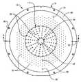
300밀리미터(mm) 실시예에서, 하부 배플판의 개구는 각각의 개구가 임의의 인접한 개구로부터 등거리가 되도록 하는 패턴으로 배열된다. 상부 배플판에는 동심원의 다중 원형(반경 방향의) 패턴으로 내부에 형성된 다소 큰 개구가 설치된다. 상부 배플판에는 또한 중앙에 위치된 충돌판(impingement plate)이 설치된다. 200mm 실시예에서, 하부 배플판의 개구는 동심원의 다중 원형(반경 방향의) 패턴으로 배열되고, 상부 배플판에는 개구가 없다.In a 300 millimeter (mm) embodiment, the openings in the lower baffle plate are arranged in a pattern such that each opening is equidistant from any adjacent opening. The upper baffle plate is provided with a rather large opening formed therein in a concentric multiple circular (radial) pattern. The upper baffle plate is also equipped with a centrally located impingement plate. In a 200 mm embodiment, the openings of the lower baffle plate are arranged in a concentric multiple circular (radial) pattern, with no openings in the upper baffle plate.
이제 도면을 참조하면, 도 1은 제1실시예의 가스 분배 또는 배플판 조립체(12)가 포함되는 애셔 처리 챔버(10)를 도시한 것이다. 내부에 설치된 배플판 조립체(12)를 가지는 애셔 처리 챔버(10)는 300밀리미터(mm) 웨이퍼 처리 시스템에서 사용하는데 적합하다. 본 발명은 포토레지스트 애셔 내에서 구현되는 것으로 도시되어 있을지라도, 잔류물 제거, 스트립핑과 같은 다른 반도체 제조 장비, 및 등방성 에칭 장비에서 사용될 수 있다.Referring now to the drawings, FIG. 1 illustrates an
배플판 조립체(12)는 일반적으로 서로 평행으로 배치되고 서로 분리되어 있는 상부 개구된 배플판(14) 및 비교적 더 큰 하부 개구된 배플판(16)을 포함한다. 배플판 조립체는 처리될 웨이퍼(22)가 배치되는 캐비티(20)를 포함하는 처리 챔버의 하부(18)에 부착된다. 서로 평행으로 되어 있는 것 이외에, 배플판(14 및 16)은 또한 처리되는 웨이퍼와 평행하게 되어 있다.The
밀봉재(23)는 배플판 조립체(12)와 처리 챔버의 하부(18)와의 사이의 인터페이스에 제공되고, 하부 배플판(16)의 홈(25) 내에 존재한다(도 2 참조). 웨이퍼는 입/출구 통로(24)를 통하여 로드 록(load lock) 메커니즘(도면에 도시되지 않음)을 통하여 처리 챔버 내에 인입되고 처리 챔버로부터 제거된다. 처리 챔버의 하부(18)에 위치된 히터 메커니즘(도면에 도시되지 않음)은 처리하는 동안 웨이퍼의 하측을 원하는 온도로 가열한다.The
도 1의 애셔 처리 챔버(10)는 전형적으로 애셔 내에서, 히터 조립체(하부)와 플라즈마 튜브 조립체(상부, 도면에 도시되지 않음) 중간에 구멍(26) 위치에서 설치된다. 플라즈마 튜브는 전형적으로 에칭 또는 다른 열화 없이, 불소 성질을 수용하도록 알루미나(Al2O3) 또는 사파이어로 이루어진다. 동작시에, 원하는 가스 혼합물은 가스 박스로부터 플라즈마 튜브내에 유입된다.The
원하는 가스 혼합물의 하나의 예는 성형 가스(forming gas)(주로 적은 비율의 수소를 갖는 질소), 및 산소이다. 어떤 처리에 대하여 애싱 비율(ashing rate)을 증가시키기 위하여 4불화 탄소(CF4)와 같은 불소 함유 가스가 가스 혼합물에 부가될 수 있다. 원하는 가스 혼합물은 마이크로웨이브 출력 발생기 조립체에 의해서 플라즈마 튜브에서 활성화되어, 처리 챔버 캐비티(20) 내에 존재하는 웨이퍼 상의 포토레지스트를 애싱하는 반응성 플라즈마를 형성한다. 활성화된 플라즈마는 플라즈마 튜브를 떠나서 대략 1.6torr의 대기압과 대략 150℃의 온도로 처리 챔버(10)내로 지향된다. 전형적으로 튜브를 통하여 아래로 그리고 처리 챔버(10)를 향하여 플라즈마를 지향시키는 플라즈마 튜브의 길이를 따라서 압력 강하가 존재한다.One example of a desired gas mixture is forming gas (mainly nitrogen with a small proportion of hydrogen), and oxygen. A fluorine containing gas such as carbon tetrafluoride (CF4 ) may be added to the gas mixture to increase the ashing rate for certain treatments. The desired gas mixture is activated in the plasma tube by the microwave output generator assembly to form a reactive plasma that ashes the photoresist on the wafer present in the
플라즈마 튜브를 떠난 활성화된 플라즈마(가스)는 배플판 조립체(12)에 도달한다. 플라즈마는 상부 배플판(14)의 개구(28) 및 하부 배플판(16)의 개구(30)를 통하여 처리 챔버 캐비티(20) 내에 분배된다. 하부 배플판(16)은 유입구(34)와 유출구(36)를 경유하여 내부 냉각 통로(32)를 통하여 흐르는 냉매로써 능동적으로 냉각될 수 있다(도 2 참조). 처리 챔버의 하부(18)의 벽(38)이 또한 유입구(42)와 유출구(44)를 경유하여 내부 냉각 통로(40)를 통하여 흐르는 냉매로 능동적으로 냉각될 수 있다.The activated plasma (gas) leaving the plasma tube reaches the
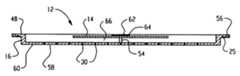
도 2의 부분 절개 사시도에 도시된 바와 같이, 하부 배플판(16)은 외부 플랜지(48), 및 개구(30)를 포함하는 일반적으로 평면의 부분(50)을 포함한다. 지지대 (54)(도 4 및 도 6에 도시됨)에 의해 상부 배플판(14)을 장착하기 위하여 하부 배플판(16)에 장착 구멍(52)이 형성되어 있다. 상부 배플판과 하부 배플판 사이의 거리는 배플판 조립체(12)를 통하는 가스 흐름의 패턴을 부분적으로 결정한다.As shown in the partial cutaway perspective view of FIG. 2, the
도 3은 도 1에 도시된 300mm 배플판 조립체의 평면도이고, 도 4는 본 실시예의 배플판 조립체의 단면도이다. 이러한 도면들에 도시된 바와 같이, 배플판 조립체는 하부 배플판 플랜지(48)의 장착 구멍(56)을 통하여 처리 챔버의 하부(18)에 장착된다. 하부 배플판(16)의 일반적으로 평면의 부분(50)은 반경 방향의 내부 부분(58)과 반경 방향의 외부 부분(60)을 포함한다.3 is a plan view of the 300 mm baffle plate assembly shown in FIG. 1, and FIG. 4 is a cross-sectional view of the baffle plate assembly of this embodiment. As shown in these figures, the baffle plate assembly is mounted to the
하부 배플판의 반경 방향의 내부 부분(58)에는 개구(30)가 제공되며, 반경 방향의 외부 부분(60)에는 제공되지 않는다. 개구(30)는 반경 방향의 내부 부분(58)을 단지 부분적으로 커버하는 것으로 도시되어 있을지라도, 실제로 이 내부 부분 전체를 커버한다(도 2 참조). 반경 방향의 내부 부분(58)의 표면적은 그 아래에 존재하는 웨이퍼(22)를 커버할만큼 충분하다(도 1 참조). 개구는 모든 방향으로 서로 등거리로 위치된다. 즉, 서로 직접적으로 인접한 임의의 세 개의 개구가 등변(等邊) 3각형을 형성한다. 상부 배플판(14)의 개구(28)는 반경 방향의(또는 동심원의 다중 원형의) 패턴으로 배열된다. 상부 배플판은 사파이어가 코팅된 용융 실리카(fused silica) 또는 석영(SiO2)으로 구성된다. 상부 배플판(14)의 개구(28)는 하부 배플판(16)의 개구(30)보다 다소 더 크다. 상부 배플판의 중앙에는 사파이어 충돌판(62)이 위치되고, 이것은 스크류(64)를 사용하여 상부 배플판에 부착된다. 사파이어 충돌판(62)은 플라즈마 튜브로부터 발산하는 활성화된 가스를 상부 배플판(14)의 나머지 개구된 영역으로 반경 방향 외측으로 전환시켜서, 처리중인 웨이퍼(22)의 반경 방향의 내부 부분이 과열되지 않도록 한다.An
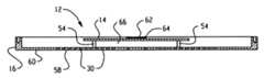
도 5 및 도 6은 200mm 웨이퍼 처리 용도로 도 1의 포토레지스트 애셔 처리 챔버 내에 설치할 수 있는, 제2실시예의 배플판 조립체(12)를 도시한 것이다. 이 제2실시예에서, 하부 배플판(16)은 반경 방향의(또는 동심원의 다중 원형의) 패턴으로 반경 방향의 내부 부분(58)에 형성된 개구(30)를 갖는다. 반경 방향의 내측 부분(58)의 표면적은 아래의 처리 챔버에 존재하는 웨이퍼(22)를 커버할만큼 충분하다.5 and 6 illustrate the
도 5 및 도 6의 본 발명의 200mm 실시예에서, 상부 배플판(14)에는 개구가 없다. 중앙에 위치한 사파이어 충돌판(62)은 본 실시예에서 유지된다. 본 실시예의 상부 배플판은 300mm 실시예와 마찬가지로, 사파이어가 코팅된 용융 실리카(석영)로 구성된다.In the 200 mm embodiment of the present invention of FIGS. 5 and 6, the
200mm 실시예 또는 300mm 실시예 중 하나에서, 하부 배플판(16)은 공지된 석영 배플판에 비하여 배플판의 열 전달 특성과 내부식성을 상당히 개선시키는 단편의 저합금 양극 처리된 알루미늄(예로서, Alcoa type C-276)으로 구성되는 것이 바람직하다. 알루미늄을 사용하면 또한 냉각 통로에 직접 구멍을 뚫거나 가공할 수 있으므로, 배플판이 가열 시스템의 불일치에 대하여 덜 민감하게 되고, 기판 표면의 처리가 대체로 균일한 온도에서 이루어지도록 한다. 알루미늄을 사용하면 또한, 온도 제어를 더 어렵게 하고 웨이퍼 소자 손상을 초래하는 가열 시스템으로부터 발산하는 높은 비율의 자외선(UV) 에너지가 차단된다.In either the 200 mm embodiment or the 300 mm embodiment, the
200mm 실시예 또는 300mm 실시예의 중 하나에서, 본 발명의 하부 배플판 조립체(16)는 플라즈마 튜브로부터 받은 반응성 플라즈마를 처리되는 웨이퍼의 표면에 걸쳐서 균일하게 분배하여 원하는 처리 결과를 달성한다. 본 발명의 배플판 조립체는 처리 중에 웨이퍼 표면을 통과하는 라디칼 밀도(radical density) 및 플라즈마 이온의 균일성을 개선시켜, 높은 웨이퍼 처리 속도를 유지하면서 개선된 처리 균일성을 제공한다. 개별적인 배플판 및 배플판 조립체의 설계는 응용 기체 역학, 재료 공학 및 처리 데이터에 의해 결정되어, 처리 챔버 내의 정확한 압력, 가스 흐름 및 온도 경사를 보장한다. 배플판 조립체는 처리 챔버(10)내에서 1인치보다 적은 수직 공간을 필요로 할 정도로 소형이다.In either the 200 mm embodiment or the 300 mm embodiment, the lower
상부 배플판(14) 바로 위로부터 하부 배플판(16) 바로 아래까지의 점진적인 압력 강하와 함께, 배플판 조립체 구성은 처리되는 웨이퍼(22)의 상부면에 걸쳐 분배되는 가스의 층류의 생성에 도움을 준다. 배플판 조립체(12)는 상기 판의 표면에 수직인 방향으로 하부 배플판의 표면에 걸쳐 단위 면적 당 질량 흐름 속도 경사를 최소화한다. 이것은 상부 판과 처리 챔버 상벽(17)(도 1 참조) 사이, 상부 및 하부 판 사이의 반경 방향의 압력 강하 효과, 및 하부 배플판에 의해서 형성되는 평면에 걸친 압력 강하 효과를 결합함으로써 달성된다. 이 효과는 웨이퍼의 표면에 반응성 종의 균일한 분배를 제공하고 반응이 발생함에 따라서 웨이퍼의 표면으로부터 발산하는 반응성 유출물을 생성하도록 하는 것이다. 배플판 조립체(12)에서 사파이어 코팅된 석영 상부 판(14)과 알루미늄 하측 판(16)을 결합하면 CF4 등 부식성 가스가 사용될 때에도, 포토레지스트 제거에 사용되는 처리 챔버에서 발견된 가혹한 조건에서 사용하는데 적합한 것으로 확인되었다.With a gradual pressure drop from just above the
동작시에, 배플판 조립체는 다음과 같은 기능을 한다. 플라즈마 튜브의 당부로부터 출력되는 (대략 1.6torr의) 활성화된 가스는 분당 약 5-7리터(lpm)의 속도로 흐른다. 상부 배플판(14)상의 사파이어 충돌판(62)은 우선 반응성 가스를 반경 방향 외부으로 분배하여, 반경 방향의 압력 강하를 발생시키는 기능을 한다. 반경 방향의 압력 강하는 상부 배플판과 하부 배플판 사이의 간격, 이러한 판들에서의 개구의 크기와 패턴, 및 이러한 판들의 크기와 형상의 함수이다. 상부 배플판(14)은 또한 플라즈마에 의한 손상으로부터 하부 배플판(16)을 보호한다.In operation, the baffle plate assembly functions as follows. Activated gas (approximately 1.6 torr) output from the sugar portion of the plasma tube flows at a rate of about 5-7 liters per minute (lpm). The
충돌판(62)과 상부 배플판(14)의 표면에서의 압력은 대략 1.5torr이다. 상부 배플판과 하부 배플판과의 사이의 영역(66)의 압력은 대략 1.2-1.3torr이다. 처리 챔버 캐비티(20)내에서, 하부 배플판(16) 아래의 압력은 1.0torr 정도이다. 플라즈마 튜브 출구로부터 처리 챔버 캐비티(20)까지의 점진적인 압력 강하는 가스의 하부 방향의 흐름을 보장하고, 배플판 조립체 구조는 이 하부 방향으로 흐르는 가스에 층류 특성을 부여한다. 점진적인 수직 방향의 압력 강하는 상부 및 하부 배플판의 개구의 수와 크기, 개구 위치, 및 조립체 기하구조의 함수이다. 하부 배플판에 걸쳐서 압력 강하가 공지되어 있기 때문에, 본 발명의 배플판 조립체에 의해서 처리된 애싱된 웨이퍼의 표면에 걸쳐 최대 5%의 애싱 비율의 비균일성 달성되었다.The pressure at the surface of the
따라서, 플라즈마 처리 시스템에서의 기판의 표면에 걸쳐서 층류의 가스 흐름을 제공하는 가스 분배판 조립체의 바람직한 실시예를 설명하였다. 그러나, 상기의 설명에 있어서, 설명은 단지 예이며, 본 발명은 본원에 설명된 특정 실시예에 국한되지 않고 이하의 청구범위 등에 의해서 규정된 바와 같이, 본 발명의 범위를 벗어나지 않고 상술된 설명과 관련된 다양한 재구성, 변형 및 대체가 실시될 수 있다는 것을 이해하여야 한다.Thus, a preferred embodiment of a gas distribution plate assembly that provides a laminar flow of gas over the surface of a substrate in a plasma processing system has been described. However, in the above description, the descriptions are merely examples, and the present invention is not limited to the specific embodiments described herein, and as defined by the following claims and the like, without departing from the scope of the present invention. It should be understood that various related reconfigurations, modifications, and substitutions may be made.
플라즈마 처리 시스템에서 처리중인 기판의 표면에 걸쳐 활성화된 가스의 층류를 가능하게 하는 메커니즘이 제공된다. 가스의 흐름은 높은 가스 흐름 속도에서도 균일한 반응 속도를 제공하는 방식으로 웨이퍼의 표면에 반응성 종을 제공하는 형태의 흐름이다. 또한, 이러한 시스템에서 웨이퍼마다의 처리 균일성을 향상시키고, 가스 분배 또는 배플판의 표면에 걸쳐 비교적 평탄한 온도 프로파일(profile)을 제공함으로써, 웨이퍼에 걸쳐서 열 경사를 최소화하는 메커니즘이 제공된다.A mechanism is provided that enables laminar flow of activated gas across the surface of a substrate being processed in a plasma processing system. Gas flow is a type of flow that provides reactive species to the surface of the wafer in a manner that provides a uniform reaction rate even at high gas flow rates. In addition, a mechanism is provided in such a system that minimizes thermal gradients across the wafer by improving processing uniformity per wafer and by providing a relatively flat temperature profile across the surface of the gas distribution or baffle plate.
Claims (24)
Translated fromKoreanApplications Claiming Priority (2)
| Application Number | Priority Date | Filing Date | Title |
|---|---|---|---|
| US09/558,606US6537419B1 (en) | 2000-04-26 | 2000-04-26 | Gas distribution plate assembly for providing laminar gas flow across the surface of a substrate |
| US09/558,606 | 2000-04-26 |
Publications (2)
| Publication Number | Publication Date |
|---|---|
| KR20010104631A KR20010104631A (en) | 2001-11-26 |
| KR100587629B1true KR100587629B1 (en) | 2006-06-08 |
Family
ID=24230206
Family Applications (1)
| Application Number | Title | Priority Date | Filing Date |
|---|---|---|---|
| KR1020010022637AExpired - LifetimeKR100587629B1 (en) | 2000-04-26 | 2001-04-26 | Gas distribution plate assembly to provide laminar flow of gas across the substrate surface |
Country Status (5)
| Country | Link |
|---|---|
| US (1) | US6537419B1 (en) |
| EP (1) | EP1150331A3 (en) |
| JP (1) | JP4998864B2 (en) |
| KR (1) | KR100587629B1 (en) |
| TW (1) | TW498450B (en) |
Cited By (1)
| Publication number | Priority date | Publication date | Assignee | Title |
|---|---|---|---|---|
| KR20200126704A (en)* | 2019-04-30 | 2020-11-09 | 피에스케이 주식회사 | A substrate processing apparatus |
Families Citing this family (43)
| Publication number | Priority date | Publication date | Assignee | Title |
|---|---|---|---|---|
| US6635117B1 (en)* | 2000-04-26 | 2003-10-21 | Axcelis Technologies, Inc. | Actively-cooled distribution plate for reducing reactive gas temperature in a plasma processing system |
| KR100516844B1 (en)* | 2001-01-22 | 2005-09-26 | 동경 엘렉트론 주식회사 | Device and method for treatment |
| CN1229855C (en)* | 2001-03-28 | 2005-11-30 | 大见忠弘 | Plasma treatment device |
| US20030234079A1 (en)* | 2002-06-19 | 2003-12-25 | Taiwan Semiconductor Manufacturing Co., Ltd. | Plasma ashing/etching using solid sapphire disk |
| US7468494B2 (en)* | 2003-01-31 | 2008-12-23 | Advanced Energy Industries | Reaction enhancing gas feed for injecting gas into a plasma chamber |
| US20040235299A1 (en)* | 2003-05-22 | 2004-11-25 | Axcelis Technologies, Inc. | Plasma ashing apparatus and endpoint detection process |
| US8580076B2 (en)* | 2003-05-22 | 2013-11-12 | Lam Research Corporation | Plasma apparatus, gas distribution assembly for a plasma apparatus and processes therewith |
| KR100526928B1 (en)* | 2003-07-16 | 2005-11-09 | 삼성전자주식회사 | Etching Apparatus |
| CN100492600C (en)* | 2003-11-05 | 2009-05-27 | 大见忠弘 | Plasma treatment device |
| US7892357B2 (en)* | 2004-01-12 | 2011-02-22 | Axcelis Technologies, Inc. | Gas distribution plate assembly for plasma reactors |
| US20050223983A1 (en)* | 2004-04-08 | 2005-10-13 | Venkat Selvamanickam | Chemical vapor deposition (CVD) apparatus usable in the manufacture of superconducting conductors |
| US20050223984A1 (en)* | 2004-04-08 | 2005-10-13 | Hee-Gyoun Lee | Chemical vapor deposition (CVD) apparatus usable in the manufacture of superconducting conductors |
| US20050241767A1 (en)* | 2004-04-30 | 2005-11-03 | Ferris David S | Multi-piece baffle plate assembly for a plasma processing system |
| US7387811B2 (en)* | 2004-09-21 | 2008-06-17 | Superpower, Inc. | Method for manufacturing high temperature superconducting conductors using chemical vapor deposition (CVD) |
| US7552521B2 (en)* | 2004-12-08 | 2009-06-30 | Tokyo Electron Limited | Method and apparatus for improved baffle plate |
| US7601242B2 (en)* | 2005-01-11 | 2009-10-13 | Tokyo Electron Limited | Plasma processing system and baffle assembly for use in plasma processing system |
| US20060225654A1 (en)* | 2005-03-29 | 2006-10-12 | Fink Steven T | Disposable plasma reactor materials and methods |
| US20080078746A1 (en) | 2006-08-15 | 2008-04-03 | Noriiki Masuda | Substrate processing system, gas supply unit, method of substrate processing, computer program, and storage medium |
| DE102007002415B4 (en)* | 2007-01-17 | 2011-04-28 | Atlas Material Testing Technology Gmbh | Device for light or weathering test comprising a sample housing with integrated UV radiation filter |
| US8715455B2 (en)* | 2007-02-06 | 2014-05-06 | Tokyo Electron Limited | Multi-zone gas distribution system for a treatment system |
| JP5192214B2 (en)* | 2007-11-02 | 2013-05-08 | 東京エレクトロン株式会社 | Gas supply apparatus, substrate processing apparatus, and substrate processing method |
| JP5474291B2 (en) | 2007-11-05 | 2014-04-16 | 株式会社アルバック | Ashing equipment |
| US8252114B2 (en)* | 2008-03-28 | 2012-08-28 | Tokyo Electron Limited | Gas distribution system and method for distributing process gas in a processing system |
| WO2009140440A1 (en)* | 2008-05-13 | 2009-11-19 | Nanoink, Inc. | Dual-tip cantilever |
| US9714465B2 (en)* | 2008-12-01 | 2017-07-25 | Applied Materials, Inc. | Gas distribution blocker apparatus |
| US8147614B2 (en)* | 2009-06-09 | 2012-04-03 | Applied Materials, Inc. | Multi-gas flow diffuser |
| KR101110080B1 (en)* | 2009-07-08 | 2012-03-13 | 주식회사 유진테크 | Substrate treatment method for selectively inserting diffusion plate |
| ITMI20100249U1 (en) | 2010-07-16 | 2012-01-17 | Alfa Laval Corp Ab | HEAT EXCHANGE DEVICE WITH REFRIGERANT FLUID DISTRIBUTION SYSTEM |
| US20120052216A1 (en)* | 2010-08-27 | 2012-03-01 | Applied Materials, Inc. | Gas distribution showerhead with high emissivity surface |
| JP5982129B2 (en)* | 2011-02-15 | 2016-08-31 | 東京エレクトロン株式会社 | Electrode and plasma processing apparatus |
| US9129778B2 (en) | 2011-03-18 | 2015-09-08 | Lam Research Corporation | Fluid distribution members and/or assemblies |
| US10316409B2 (en)* | 2012-12-21 | 2019-06-11 | Novellus Systems, Inc. | Radical source design for remote plasma atomic layer deposition |
| CN104112637A (en)* | 2013-04-17 | 2014-10-22 | 北京北方微电子基地设备工艺研究中心有限责任公司 | Air inlet system and plasma processing device |
| JP1545606S (en)* | 2015-08-26 | 2016-03-14 | ||
| US10604841B2 (en) | 2016-12-14 | 2020-03-31 | Lam Research Corporation | Integrated showerhead with thermal control for delivering radical and precursor gas to a downstream chamber to enable remote plasma film deposition |
| JP6988209B2 (en) | 2017-07-11 | 2022-01-05 | 株式会社Ihi | Fluid disperser and fluid disperser |
| WO2019113478A1 (en) | 2017-12-08 | 2019-06-13 | Lam Research Corporation | Integrated showerhead with improved hole pattern for delivering radical and precursor gas to a downstream chamber to enable remote plasma film deposition |
| US10876208B2 (en) | 2018-01-16 | 2020-12-29 | Taiwan Semiconductor Manufacturing Company Ltd. | Apparatus and method for fabricating a semiconductor device |
| WO2022114583A1 (en)* | 2020-11-24 | 2022-06-02 | 한국전자기술연구원 | Showerhead and thin film deposition device including same |
| CN113441032B (en)* | 2021-06-25 | 2022-09-16 | 北京北方华创微电子装备有限公司 | Semiconductor process equipment and gas conveying device thereof |
| US11448977B1 (en) | 2021-09-24 | 2022-09-20 | Applied Materials, Inc. | Gas distribution plate with UV blocker at the center |
| US20240006157A1 (en)* | 2022-07-01 | 2024-01-04 | Taiwan Semiconductor Manufacturing Company | Methods and systems for dry etching |
| USD1037778S1 (en)* | 2022-07-19 | 2024-08-06 | Applied Materials, Inc. | Gas distribution plate |
Citations (4)
| Publication number | Priority date | Publication date | Assignee | Title |
|---|---|---|---|---|
| JPS5938374A (en)* | 1982-08-26 | 1984-03-02 | Canon Inc | Plasma CVD equipment |
| JPH08213320A (en)* | 1994-09-26 | 1996-08-20 | Applied Materials Inc | Electrode between sputtering target and workpiece |
| US5558717A (en)* | 1994-11-30 | 1996-09-24 | Applied Materials | CVD Processing chamber |
| KR19990009886U (en)* | 1997-08-26 | 1999-03-15 | 구본준 | Semiconductor Plasma Deposition Apparatus |
Family Cites Families (12)
| Publication number | Priority date | Publication date | Assignee | Title |
|---|---|---|---|---|
| US4595484A (en)* | 1985-12-02 | 1986-06-17 | International Business Machines Corporation | Reactive ion etching apparatus |
| US5212116A (en)* | 1990-06-18 | 1993-05-18 | At&T Bell Laboratories | Method for forming planarized films by preferential etching of the center of a wafer |
| JPH04236425A (en)* | 1991-01-21 | 1992-08-25 | Toshiba Corp | Plasma processing equipment |
| JPH05184977A (en)* | 1992-01-09 | 1993-07-27 | Toshiba Corp | Shower nozzle |
| US5449410A (en) | 1993-07-28 | 1995-09-12 | Applied Materials, Inc. | Plasma processing apparatus |
| US5647911A (en) | 1993-12-14 | 1997-07-15 | Sony Corporation | Gas diffuser plate assembly and RF electrode |
| US5653806A (en) | 1995-03-10 | 1997-08-05 | Advanced Technology Materials, Inc. | Showerhead-type discharge assembly for delivery of source reagent vapor to a substrate, and CVD process utilizing same |
| JP3077582B2 (en)* | 1996-02-21 | 2000-08-14 | 日本電気株式会社 | Plasma CVD apparatus and cleaning method therefor |
| US5968275A (en)* | 1997-06-25 | 1999-10-19 | Lam Research Corporation | Methods and apparatus for passivating a substrate in a plasma reactor |
| US6155200A (en)* | 1997-07-08 | 2000-12-05 | Tokyo Electron Limited | ECR plasma generator and an ECR system using the generator |
| US6110556A (en)* | 1997-10-17 | 2000-08-29 | Applied Materials, Inc. | Lid assembly for a process chamber employing asymmetric flow geometries |
| US6635117B1 (en)* | 2000-04-26 | 2003-10-21 | Axcelis Technologies, Inc. | Actively-cooled distribution plate for reducing reactive gas temperature in a plasma processing system |
- 2000
- 2000-04-26USUS09/558,606patent/US6537419B1/ennot_activeExpired - Fee Related
- 2001
- 2001-04-17TWTW090109106Apatent/TW498450B/ennot_activeIP Right Cessation
- 2001-04-25EPEP01303758Apatent/EP1150331A3/ennot_activeWithdrawn
- 2001-04-25JPJP2001128061Apatent/JP4998864B2/ennot_activeExpired - Lifetime
- 2001-04-26KRKR1020010022637Apatent/KR100587629B1/ennot_activeExpired - Lifetime
Patent Citations (4)
| Publication number | Priority date | Publication date | Assignee | Title |
|---|---|---|---|---|
| JPS5938374A (en)* | 1982-08-26 | 1984-03-02 | Canon Inc | Plasma CVD equipment |
| JPH08213320A (en)* | 1994-09-26 | 1996-08-20 | Applied Materials Inc | Electrode between sputtering target and workpiece |
| US5558717A (en)* | 1994-11-30 | 1996-09-24 | Applied Materials | CVD Processing chamber |
| KR19990009886U (en)* | 1997-08-26 | 1999-03-15 | 구본준 | Semiconductor Plasma Deposition Apparatus |
Cited By (3)
| Publication number | Priority date | Publication date | Assignee | Title |
|---|---|---|---|---|
| KR20200126704A (en)* | 2019-04-30 | 2020-11-09 | 피에스케이 주식회사 | A substrate processing apparatus |
| KR102187121B1 (en)* | 2019-04-30 | 2020-12-07 | 피에스케이 주식회사 | A substrate processing apparatus |
| US11139152B2 (en) | 2019-04-30 | 2021-10-05 | Psk Inc. | Substrate processing apparatus |
Also Published As
| Publication number | Publication date |
|---|---|
| TW498450B (en) | 2002-08-11 |
| KR20010104631A (en) | 2001-11-26 |
| JP2002057146A (en) | 2002-02-22 |
| JP4998864B2 (en) | 2012-08-15 |
| US6537419B1 (en) | 2003-03-25 |
| EP1150331A2 (en) | 2001-10-31 |
| EP1150331A3 (en) | 2003-10-22 |
Similar Documents
| Publication | Publication Date | Title |
|---|---|---|
| KR100587629B1 (en) | Gas distribution plate assembly to provide laminar flow of gas across the substrate surface | |
| US7892357B2 (en) | Gas distribution plate assembly for plasma reactors | |
| EP1150330B1 (en) | Actively-cooled distribution plate for reducing reactive gas temperature in a plasma processing system | |
| KR101411674B1 (en) | High temperature chamber process and chamber design for photoresist strips and post metal etch passivation | |
| EP1741124B1 (en) | Segmented baffle plate assembly for a plasma processing system | |
| US6225745B1 (en) | Dual plasma source for plasma process chamber | |
| JP4649088B2 (en) | Cooling ceiling for plasma reactor with small gas distribution plate array that is insulated and plasma heated | |
| KR101170861B1 (en) | Plasma ashing process for increasing photoresist removal rate and plasma apparatus with cooling means | |
| KR20040079993A (en) | Reactor assembly and processing method | |
| KR20060003121A (en) | Plasma apparatus, gas distribution assembly for plasma apparatus and process accordingly | |
| JP2009071334A (en) | Method and apparatus for treating surface | |
| CN114868238A (en) | Targeted heating control system | |
| JP2008113033A (en) | Method of surface treatment, and its equipment |
Legal Events
| Date | Code | Title | Description |
|---|---|---|---|
| PA0109 | Patent application | Patent event code:PA01091R01D Comment text:Patent Application Patent event date:20010426 | |
| PG1501 | Laying open of application | ||
| A201 | Request for examination | ||
| PA0201 | Request for examination | Patent event code:PA02012R01D Patent event date:20031030 Comment text:Request for Examination of Application Patent event code:PA02011R01I Patent event date:20010426 Comment text:Patent Application | |
| E902 | Notification of reason for refusal | ||
| PE0902 | Notice of grounds for rejection | Comment text:Notification of reason for refusal Patent event date:20050822 Patent event code:PE09021S01D | |
| E701 | Decision to grant or registration of patent right | ||
| PE0701 | Decision of registration | Patent event code:PE07011S01D Comment text:Decision to Grant Registration Patent event date:20060509 | |
| GRNT | Written decision to grant | ||
| PR0701 | Registration of establishment | Comment text:Registration of Establishment Patent event date:20060530 Patent event code:PR07011E01D | |
| PR1002 | Payment of registration fee | Payment date:20060530 End annual number:3 Start annual number:1 | |
| PG1601 | Publication of registration | ||
| PR1001 | Payment of annual fee | Payment date:20090409 Start annual number:4 End annual number:4 | |
| PR1001 | Payment of annual fee | Payment date:20100429 Start annual number:5 End annual number:5 | |
| PR1001 | Payment of annual fee | Payment date:20110428 Start annual number:6 End annual number:6 | |
| PR1001 | Payment of annual fee | Payment date:20120427 Start annual number:7 End annual number:7 | |
| FPAY | Annual fee payment | Payment date:20130509 Year of fee payment:8 | |
| PR1001 | Payment of annual fee | Payment date:20130509 Start annual number:8 End annual number:8 | |
| FPAY | Annual fee payment | Payment date:20140514 Year of fee payment:9 | |
| PR1001 | Payment of annual fee | Payment date:20140514 Start annual number:9 End annual number:9 | |
| FPAY | Annual fee payment | Payment date:20150512 Year of fee payment:10 | |
| PR1001 | Payment of annual fee | Payment date:20150512 Start annual number:10 End annual number:10 | |
| FPAY | Annual fee payment | Payment date:20160513 Year of fee payment:11 | |
| PR1001 | Payment of annual fee | Payment date:20160513 Start annual number:11 End annual number:11 | |
| PC1801 | Expiration of term | Termination date:20211026 Termination category:Expiration of duration |