KR100587367B1 - Transverse electric field liquid crystal display device and manufacturing method thereof - Google Patents
Transverse electric field liquid crystal display device and manufacturing method thereofDownload PDFInfo
- Publication number
- KR100587367B1 KR100587367B1KR1020000061934AKR20000061934AKR100587367B1KR 100587367 B1KR100587367 B1KR 100587367B1KR 1020000061934 AKR1020000061934 AKR 1020000061934AKR 20000061934 AKR20000061934 AKR 20000061934AKR 100587367 B1KR100587367 B1KR 100587367B1
- Authority
- KR
- South Korea
- Prior art keywords
- data
- forming
- liquid crystal
- electrode
- crystal display
- Prior art date
- Legal status (The legal status is an assumption and is not a legal conclusion. Google has not performed a legal analysis and makes no representation as to the accuracy of the status listed.)
- Expired - Lifetime
Links
Images


Classifications
- G—PHYSICS
- G02—OPTICS
- G02F—OPTICAL DEVICES OR ARRANGEMENTS FOR THE CONTROL OF LIGHT BY MODIFICATION OF THE OPTICAL PROPERTIES OF THE MEDIA OF THE ELEMENTS INVOLVED THEREIN; NON-LINEAR OPTICS; FREQUENCY-CHANGING OF LIGHT; OPTICAL LOGIC ELEMENTS; OPTICAL ANALOGUE/DIGITAL CONVERTERS
- G02F1/00—Devices or arrangements for the control of the intensity, colour, phase, polarisation or direction of light arriving from an independent light source, e.g. switching, gating or modulating; Non-linear optics
- G02F1/01—Devices or arrangements for the control of the intensity, colour, phase, polarisation or direction of light arriving from an independent light source, e.g. switching, gating or modulating; Non-linear optics for the control of the intensity, phase, polarisation or colour
- G02F1/13—Devices or arrangements for the control of the intensity, colour, phase, polarisation or direction of light arriving from an independent light source, e.g. switching, gating or modulating; Non-linear optics for the control of the intensity, phase, polarisation or colour based on liquid crystals, e.g. single liquid crystal display cells
- G02F1/133—Constructional arrangements; Operation of liquid crystal cells; Circuit arrangements
- G02F1/1333—Constructional arrangements; Manufacturing methods
- G02F1/1335—Structural association of cells with optical devices, e.g. polarisers or reflectors
- G02F1/133509—Filters, e.g. light shielding masks
- G02F1/133512—Light shielding layers, e.g. black matrix
- G—PHYSICS
- G02—OPTICS
- G02F—OPTICAL DEVICES OR ARRANGEMENTS FOR THE CONTROL OF LIGHT BY MODIFICATION OF THE OPTICAL PROPERTIES OF THE MEDIA OF THE ELEMENTS INVOLVED THEREIN; NON-LINEAR OPTICS; FREQUENCY-CHANGING OF LIGHT; OPTICAL LOGIC ELEMENTS; OPTICAL ANALOGUE/DIGITAL CONVERTERS
- G02F1/00—Devices or arrangements for the control of the intensity, colour, phase, polarisation or direction of light arriving from an independent light source, e.g. switching, gating or modulating; Non-linear optics
- G02F1/01—Devices or arrangements for the control of the intensity, colour, phase, polarisation or direction of light arriving from an independent light source, e.g. switching, gating or modulating; Non-linear optics for the control of the intensity, phase, polarisation or colour
- G02F1/13—Devices or arrangements for the control of the intensity, colour, phase, polarisation or direction of light arriving from an independent light source, e.g. switching, gating or modulating; Non-linear optics for the control of the intensity, phase, polarisation or colour based on liquid crystals, e.g. single liquid crystal display cells
- G02F1/133—Constructional arrangements; Operation of liquid crystal cells; Circuit arrangements
- G02F1/136—Liquid crystal cells structurally associated with a semi-conducting layer or substrate, e.g. cells forming part of an integrated circuit
- G—PHYSICS
- G02—OPTICS
- G02F—OPTICAL DEVICES OR ARRANGEMENTS FOR THE CONTROL OF LIGHT BY MODIFICATION OF THE OPTICAL PROPERTIES OF THE MEDIA OF THE ELEMENTS INVOLVED THEREIN; NON-LINEAR OPTICS; FREQUENCY-CHANGING OF LIGHT; OPTICAL LOGIC ELEMENTS; OPTICAL ANALOGUE/DIGITAL CONVERTERS
- G02F1/00—Devices or arrangements for the control of the intensity, colour, phase, polarisation or direction of light arriving from an independent light source, e.g. switching, gating or modulating; Non-linear optics
- G02F1/01—Devices or arrangements for the control of the intensity, colour, phase, polarisation or direction of light arriving from an independent light source, e.g. switching, gating or modulating; Non-linear optics for the control of the intensity, phase, polarisation or colour
- G02F1/13—Devices or arrangements for the control of the intensity, colour, phase, polarisation or direction of light arriving from an independent light source, e.g. switching, gating or modulating; Non-linear optics for the control of the intensity, phase, polarisation or colour based on liquid crystals, e.g. single liquid crystal display cells
- G02F1/133—Constructional arrangements; Operation of liquid crystal cells; Circuit arrangements
- G02F1/1333—Constructional arrangements; Manufacturing methods
- G02F1/1343—Electrodes
- G02F1/134309—Electrodes characterised by their geometrical arrangement
- G02F1/134363—Electrodes characterised by their geometrical arrangement for applying an electric field parallel to the substrate, i.e. in-plane switching [IPS]
- G—PHYSICS
- G02—OPTICS
- G02F—OPTICAL DEVICES OR ARRANGEMENTS FOR THE CONTROL OF LIGHT BY MODIFICATION OF THE OPTICAL PROPERTIES OF THE MEDIA OF THE ELEMENTS INVOLVED THEREIN; NON-LINEAR OPTICS; FREQUENCY-CHANGING OF LIGHT; OPTICAL LOGIC ELEMENTS; OPTICAL ANALOGUE/DIGITAL CONVERTERS
- G02F1/00—Devices or arrangements for the control of the intensity, colour, phase, polarisation or direction of light arriving from an independent light source, e.g. switching, gating or modulating; Non-linear optics
- G02F1/01—Devices or arrangements for the control of the intensity, colour, phase, polarisation or direction of light arriving from an independent light source, e.g. switching, gating or modulating; Non-linear optics for the control of the intensity, phase, polarisation or colour
- G02F1/13—Devices or arrangements for the control of the intensity, colour, phase, polarisation or direction of light arriving from an independent light source, e.g. switching, gating or modulating; Non-linear optics for the control of the intensity, phase, polarisation or colour based on liquid crystals, e.g. single liquid crystal display cells
- G02F1/133—Constructional arrangements; Operation of liquid crystal cells; Circuit arrangements
- G02F1/1333—Constructional arrangements; Manufacturing methods
- G02F1/133397—Constructional arrangements; Manufacturing methods for suppressing after-image or image-sticking
- G—PHYSICS
- G02—OPTICS
- G02F—OPTICAL DEVICES OR ARRANGEMENTS FOR THE CONTROL OF LIGHT BY MODIFICATION OF THE OPTICAL PROPERTIES OF THE MEDIA OF THE ELEMENTS INVOLVED THEREIN; NON-LINEAR OPTICS; FREQUENCY-CHANGING OF LIGHT; OPTICAL LOGIC ELEMENTS; OPTICAL ANALOGUE/DIGITAL CONVERTERS
- G02F1/00—Devices or arrangements for the control of the intensity, colour, phase, polarisation or direction of light arriving from an independent light source, e.g. switching, gating or modulating; Non-linear optics
- G02F1/01—Devices or arrangements for the control of the intensity, colour, phase, polarisation or direction of light arriving from an independent light source, e.g. switching, gating or modulating; Non-linear optics for the control of the intensity, phase, polarisation or colour
- G02F1/13—Devices or arrangements for the control of the intensity, colour, phase, polarisation or direction of light arriving from an independent light source, e.g. switching, gating or modulating; Non-linear optics for the control of the intensity, phase, polarisation or colour based on liquid crystals, e.g. single liquid crystal display cells
- G02F1/133—Constructional arrangements; Operation of liquid crystal cells; Circuit arrangements
- G02F1/136—Liquid crystal cells structurally associated with a semi-conducting layer or substrate, e.g. cells forming part of an integrated circuit
- G02F1/1362—Active matrix addressed cells
- G02F1/136286—Wiring, e.g. gate line, drain line
- G—PHYSICS
- G02—OPTICS
- G02F—OPTICAL DEVICES OR ARRANGEMENTS FOR THE CONTROL OF LIGHT BY MODIFICATION OF THE OPTICAL PROPERTIES OF THE MEDIA OF THE ELEMENTS INVOLVED THEREIN; NON-LINEAR OPTICS; FREQUENCY-CHANGING OF LIGHT; OPTICAL LOGIC ELEMENTS; OPTICAL ANALOGUE/DIGITAL CONVERTERS
- G02F2201/00—Constructional arrangements not provided for in groups G02F1/00 - G02F7/00
- G02F2201/12—Constructional arrangements not provided for in groups G02F1/00 - G02F7/00 electrode
- G02F2201/122—Constructional arrangements not provided for in groups G02F1/00 - G02F7/00 electrode having a particular pattern
Landscapes
- Physics & Mathematics (AREA)
- Nonlinear Science (AREA)
- Mathematical Physics (AREA)
- Chemical & Material Sciences (AREA)
- Crystallography & Structural Chemistry (AREA)
- General Physics & Mathematics (AREA)
- Optics & Photonics (AREA)
- Geometry (AREA)
- Liquid Crystal (AREA)
- Engineering & Computer Science (AREA)
- Microelectronics & Electronic Packaging (AREA)
Abstract
Translated fromKoreanDescription
Translated fromKorean도 1a는 종래 기술에 따른 횡전계방식 액정표시소자의 평면도.Figure 1a is a plan view of a transverse electric field type liquid crystal display device according to the prior art.
삭제delete
도 1b는 도 1a의 절단면 A-A'를 나타낸 단면도.FIG. 1B is a cross-sectional view taken along the line A-A 'of FIG. 1A; FIG.
도 1c는 도 1a의 절단면 B-B'를 나타낸 단면도.FIG. 1C is a cross-sectional view illustrating the cut surface BB ′ in FIG. 1A. FIG.
도 2는 횡전계방식 액정표시소자의 ITO-ITO전극 구조를 나타낸 평면도.2 is a plan view showing the structure of the ITO-ITO electrode of the transverse electric field liquid crystal display device.
도 3a는 데이터 전극에 DC 정(+)전압이 인가될 경우의 투과영역 및 차광영역을 나타낸 도면.3A is a view showing a transmission area and a light blocking area when a DC positive voltage is applied to a data electrode.
도 3b는 데이터 전극에 DC 부(-)전압이 인가될 경우의 투과영역 및 차광영역을 나타낸 도면.3B is a view showing a transmission area and a light blocking area when a DC negative voltage is applied to the data electrode.
도 4a는 본 발명의 제 1 실시예에 따른 횡전계방식 액정표시장치의 요부 단면도.4A is a cross-sectional view illustrating main parts of a transverse electric field type liquid crystal display device according to a first embodiment of the present invention;
도 4b는 본 발명의 제 2 실시예에 따른 횡전계방식 액정표시장치의 요부 단면도.4B is a cross-sectional view illustrating main parts of a transverse electric field type liquid crystal display device according to a second exemplary embodiment of the present invention.
도 4c는 본 발명의 제 3 실시예에 따른 횡전계방식 액정표시장치의 요부 단면도.4C is a cross-sectional view illustrating main parts of a transverse electric field type liquid crystal display device according to a third exemplary embodiment of the present invention.
도 5는 본 발명의 제 1 내지 제 4 실시예에서의 디스플레이 상의 화면을 나타낸 도면.5 shows screens on a display in the first to fourth embodiments of the present invention.
도 6a는 본 발명의 제 5 실시예에 따른 횡전계방식 액정표시장치의 요부 단면도.6A is a cross-sectional view illustrating main parts of a transverse electric field type liquid crystal display device according to a fifth embodiment of the present invention;
도 6b는 본 발명의 제 6 실시예에 따른 횡전계방식 액정표시장치의 요부 단면도.6B is a cross-sectional view illustrating main parts of a transverse electric field type liquid crystal display device according to a sixth embodiment of the present invention;
도 6c는 본 발명의 제 7 실시예에 따른 횡전계방식 액정표시장치의 요부 단면도.6C is a cross-sectional view illustrating main parts of a transverse electric field type liquid crystal display device according to a seventh exemplary embodiment of the present invention.
도 7은 본 발명의 제 5 내지 제 7 실시예에서의 디스플레이 상의 화면을 나타낸 도면.Fig. 7 shows a screen on a display in the fifth to seventh embodiments of the present invention.
*도면의 주요 부분에 대한 부호설명* Explanation of symbols on the main parts of the drawings
213 : 공통전극 214 : 데이터 전극213: common electrode 214: data electrode
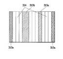
215a, 215b : 차광층 325 : 절연층215a, 215b: Light shielding layer 325: Insulation layer
본 발명은 액정표시소자(LCD ; Liquid Crystal Display Device)에 관한 것으로, 특히 인가 전압의 정부에 관계없이 일정한 휘도를 나타내는 횡전계방식 액정표시소자 및 그 제조방법에 관한 것이다.BACKGROUND OF THE INVENTION 1. Field of the Invention The present invention relates to a liquid crystal display device (LCD), and more particularly, to a transverse electric field type liquid crystal display device having a constant luminance regardless of the applied voltage.
현재 주로 사용되고 있는 액정표시소자 중 하나로 트위스트 네마틱(TN : twisted nematic) 방식의 액정표시소자를 들 수 있다. 상기 트위스트 네마틱 방식은 두 기판에 각각 전극을 설치하고 액정 방향자가 90°트위스트 되도록 배열한 다음 전극에 전압을 가하여 액정 방향자를 구동하는 방식이다.One of the liquid crystal display devices currently used is a twisted nematic (TN) type liquid crystal display device. The twisted nematic method is a method of driving the liquid crystal director by installing electrodes on two substrates, arranging the liquid crystal directors to be twisted by 90 °, and then applying a voltage to the electrodes.
그러나, 상기 TN방식(twisted nematic mode) 액정표시소자는 시야각이 좁다는 큰 단점이 있다.However, the TN (twisted nematic mode) liquid crystal display device has a big disadvantage that the viewing angle is narrow.
그래서, 최근에 상기 협소한 시야각 문제를 해결하기 위하여 여러 가지 새로운 방식을 채용한 액정표시소자에 대한 연구가 활발하게 진행되고 있는데, 상기 방식으로 횡전계방식(IPS:in-plane switching mode) 또는 OCB방식(optically compensated birefrigence mode) 등이 있다.Recently, researches on liquid crystal display devices employing various new methods have been actively conducted to solve the narrow viewing angle problem. In this method, an in-plane switching mode (IPS) or an OCB is used. Optically compensated birefrigence mode.
이 가운데 상기 횡전계방식 액정표시소자는 액정 분자를 기판에 대해서 수평을 유지한 상태로 회전시키기 위하여 2개의 전극을 동일한 기판 상에 형성하고, 상기 2개의 전극 사이에 전압을 인가하여 기판에 대해서 수평방향으로 전계를 발생시킨다. 즉, 액정 분자의 장축이 기판에 대하여 일어서지 않게 된다.Among these, the transverse electric field type liquid crystal display device has two electrodes formed on the same substrate to rotate the liquid crystal molecules in a horizontal state with respect to the substrate, and applies a voltage between the two electrodes so as to be horizontal with respect to the substrate. Generate an electric field in the direction. In other words, the long axis of the liquid crystal molecules does not stand on the substrate.
이 때문에, 시각방향에 대한 액정의 복굴절의 변화가 작아 종래의 TN방식 액정표시소자에 비해 시야각 특성이 월등하게 우수하다.For this reason, the change of the birefringence of the liquid crystal with respect to the visual direction is small, and the viewing angle characteristic is much superior to the conventional TN type liquid crystal display device.
이하, 첨부된 도면을 참조하여 종래 기술의 횡전계방식 액정표시소자의 구조를 설명하면 다음과 같다.Hereinafter, a structure of a transverse electric field type liquid crystal display device according to the related art will be described with reference to the accompanying drawings.
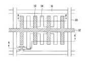
도 1a는 종래 기술에 따른 평면구동방식 액정표시소자의 평면도이고, 도 1b는 도 1a의 절단면 A-A'를 나타낸 단면도이고, 도 1c는 도 1a의 절단면 B-B'를 나타낸 단면도이다.FIG. 1A is a plan view of a planar drive type liquid crystal display device according to the prior art, FIG. 1B is a cross-sectional view showing a cutting plane A-A 'of FIG. 1A, and FIG. 1C is a cross-sectional view showing a cutting plane B-B' of FIG.
일반적인 횡전계방식 액정표시소자는 도 1a에서와 같이, 제 1 기판 위에 배열되어 화소영역을 정의하는 데이터배선(10) 및 게이트배선(11)과, 상기한 게이트배선(11)과 평행하게 화소내에 배열된 공통배선(12)과, 상기한 게이트배선(11)과 데이터배선(10)의 교차점에 배치된 박막트랜지스터와, 상기한 화소내에 데이터배선(10)과 평행하게 배열된 데이터전극(14) 및 공통전극(13)으로 구성된다.A general transverse electric field type liquid crystal display device has a
도 1b를 참고로 좀 더 상세히 살펴보면, 종래 기술에 따른 횡전계방식 액정표시소자는 제 1 기판(18)과 제 2 기판(19)을 대향 합착하여 상기 두 기판 사이에 액정층(30)을 주입하여 형성하는데, 먼저, 상기 제 1 기판(18) 상에 금속을 증착하여 복수개의 게이트 배선과, 상기 게이트 배선에서 분기되어 박막트랜지스터 위치에 형성된 게이트전극(9)을 패터닝한다.Referring to FIG. 1B, a transverse electric field type liquid crystal display device according to the related art injects a
다음, 상기 게이트 전극(9)을 포함한 전면에 게이트 절연막(20)을 형성하고, 상기 게이트 절연막(20) 상부에 상기 게이트 배선과 매트릭스 구조를 이루도록 데이터 배선(10)을 형성한다.Next, a
이 때, 상기 데이터배선(10) 형성시, 박막트랜지스터의 소스/드레인 전극(16/17)을 동시에 형성하며, 상기 소스/드레인 전극(16/17) 아래에는 액티브층을 이루는 반도체층(15)이 형성되어 있다.At this time, when the
이후, 상기 드레인 전극(17)과 전기적으로 연결되며 상기 데이터 배선(10)에 평행하도록 데이터전극(14)을 형성하고, 상기 데이터전극(14) 상에서 상기 게이트 배선에 평행하도록 공통배선(12)을 형성한다.Thereafter, a
이후, 공통전극(13)을 형성하는데, 상기 공통전극(13)은 데이터전극(14)과 동일 평면상에 형성하거나 또는, 도 1b에 도시된 바와 같이, 절연막(보호막, 25)을 사이에 두고 서로 다른 평면상에 형성한다.Thereafter, the
이 때, 상기 데이터전극(14) 및 공통전극(13)은 빛이 잘 투과되는 투명도전막인 ITO(Indium Tin Oxide)로 형성되며 이 때의 액정표시소자를 ITO-ITO전극 횡전계방식 액정표시소자라 부르기도 한다.In this case, the
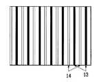
상기 ITO-ITO전극 구조는 도 2에서와 같다.The ITO-ITO electrode structure is the same as in FIG.
한편, 상기 제 2 기판(19) 상에는 빛의 누설을 방지하는 블랙 매트릭스(21)을 형성하고, 상기 블랙 매트릭스(21) 사이사이에 R, G 및 B의 칼라필터 패턴으로 이루어진 칼라필터층(22)을 형성한다.On the other hand, a
이 때, 상기 블랙 매트릭스(21)는 단위화소 내에 형성된 복수개의 공통전극들 중 가장 바깥쪽에 위치하는 공통전극의 상부에까지 형성시켜서 빛을 차광한다.In this case, the
그리고 상기 컬러필터층 상부에 컬러필터층(22)을 보호하는 오버코트층(23)을 형성한다.An
그런데, 이와 같이 구성된 ITO-ITO 횡전계방식 액정표시소자는 DC전압을 인가할 경우 인가전압의 정(+), 부(-)에 따라 빛이 투과되는 전극이 달라진다.However, in the ITO-ITO transverse electric field type liquid crystal display device configured as described above, when a DC voltage is applied, an electrode through which light is transmitted varies according to the positive (+) and the negative (-) of the applied voltage.
즉, 데이터전극(14)에 DC(Direct Current) 정(+) 전압이 인가되면 도 3a에서와 같이 공통전극(13)에서 빛이 투과되고, 데이터전극(14)에 DC 부(-) 전압 인가되면 도 3b에서와 같이 데이터전극(14)에서 빛이 투과된다.That is, when a direct current (DC) voltage is applied to the
참고적으로, 도 3a는 데이터 전극에 DC 정(+)전압이 인가될 경우의 투과영역 및 차광영역을 도시한 것이고, 도 3b는 데이터 전극에 DC 부(-)전압이 인가될 경우 의 투과영역 및 차광영역을 도시한 것이다.For reference, FIG. 3A illustrates a transmission region and a light blocking region when a DC positive voltage is applied to the data electrode, and FIG. 3B illustrates a transmission region when a DC negative voltage is applied to the data electrode. And a light shielding area.
그러나, 상기와 같은 종래의 횡전계방식 액정표시소자는 다음과 같은 문제점이 있다.However, the conventional transverse electric field type liquid crystal display device as described above has the following problems.
단위화소내 가장 바깥쪽에 위치한 공통전극과 액정간의 이상 현상에 의한 화질 저하를 개선시킬 목적으로 상기 가장 바깥쪽에 위치한 공통전극을 대향기판의 블랙매트릭스층으로 차광할 경우, 단위화소내 데이터전극과 공통전극의 투과면적이 서로 달라지게 되어 인가전압의 정(+), 부(-)에 따라 휘도차가 발생하게 되고, 이러한 휘도차에 의해 플리커(flicker) 및 잔상이 발생하여 디스플레이 소자로서의 신뢰성을 저하된다.When the outermost common electrode is shielded by the black matrix layer of the opposing substrate in order to improve image quality deterioration due to anomalous phenomenon between the outermost common electrode and the liquid crystal in the unit pixel, the data electrode and the common electrode in the unit pixel are shielded. The transmissive areas of the light beams are different from each other, so that a difference in luminance occurs depending on the positive (+) and negative (-) values of the applied voltage. Flicker and afterimages occur due to the luminance difference, thereby degrading reliability as a display element.
본 발명은 상기와 같은 문제점을 해결하기 위하여 안출한 것으로 전압 인가시, 데이터전극과 공통전극간의 빛의 투과면적이 동일해지도록 함으로써 화질을 개선시킬 수 있는 횡전계방식 액정표시장치 및 그 제조방법을 제공하는데 그 목적이 있다.The present invention has been made to solve the above problems, and when a voltage is applied, a transverse electric field type liquid crystal display device and a method of manufacturing the same which can improve image quality by making the transmission area of light between the data electrode and the common electrode the same. The purpose is to provide.
상기와 같은 목적을 달성하기 위한 본 발명의 횡전계방식 액정표시장치는 제 1 기판 및 제 2 기판과, 상기 제 1 기판상에 정의된 복수의 화소영역과, 상기 각 화소영역에 교번하여 형성되며 전압 인가에 따라 동일한 광 투과면적을 갖도록 패터닝된 데이터 전극 및 공통전극과, 상기 제 1 기판과 제 2 기판 사이에 형성된 액정층을 포함하여 구성되고, 본 발명의 횡전계방식 액정표시장치 제조방법은 제 1 기판과 제 2 기판을 준비하는 단계와, 상기 제 1 기판상에 복수의 게이트 배선과 데이터 배선을 형성하여 복수의 화소영역을 정의하는 단계와, 상기 각 화소영역에 서로 교번하여 형성되며 전압인가시 동일한 광 투과면적을 갖도록 복수의 데이터 전극과 공통전극을 형성하는 단계와, 상기 제 1 기판과 제 2 기판 사이에 액정층을 형성하는 단계를 포함하여 이루어지는 것을 특징으로 한다.The transverse electric field liquid crystal display device of the present invention for achieving the above object is formed by alternating between the first substrate and the second substrate, a plurality of pixel regions defined on the first substrate, and each pixel region. The method includes a data electrode and a common electrode patterned to have the same light transmission area according to voltage application, and a liquid crystal layer formed between the first and second substrates. Preparing a first substrate and a second substrate, defining a plurality of pixel regions by forming a plurality of gate wirings and data wirings on the first substrate, and alternately forming voltages in the pixel regions. Forming a plurality of data electrodes and a common electrode to have the same light transmission area upon application, and forming a liquid crystal layer between the first substrate and the second substrate. Characterized in that made.
이하, 첨부된 도면을 참조하여 본 발명의 실시예에 따른 횡전계방식 액정표시장치 및 그 제조방법을 상세히 설명하면 다음과 같다.Hereinafter, a transverse electric field type liquid crystal display device and a manufacturing method thereof according to an embodiment of the present invention will be described in detail with reference to the accompanying drawings.
도 4a는 본 발명의 제 1 실시예에 따른 횡전계방식 액정표시장치의 요부 단면도로서, 도면에는 도시되지 않았지만, 제 1 기판 상에 금속을 증착하여 게이트 배선과, 상기 게이트 배선에서 분기되는 박막트랜지스터의 게이트전극을 패터닝한다.FIG. 4A is a cross-sectional view illustrating main parts of a transverse electric field type liquid crystal display device according to a first exemplary embodiment of the present invention. Although not shown in the drawing, a metal film is deposited on a first substrate to form a gate wiring and a thin film transistor branched from the gate wiring. The gate electrode of is patterned.
다음, 상기 게이트 배선을 포함한 전면에 게이트 절연막을 형성하고, 상기 게이트 절연막 상부에 상기 게이트 배선과 매트릭스 배열 구조를 이루어 단위화소 영역을 구분짓도록 데이터 배선을 형성한다.Next, a gate insulating film is formed on the entire surface including the gate wiring, and a data wiring is formed on the gate insulating film to form a matrix array structure to distinguish unit pixel regions.
이 때, 상기 데이터 배선과 동시에 박막트랜지스터 위치에 소스/드레인 전극을 형성한다. 한편, 상기 소스/드레인 전극 아래에 액티브층을 이루는 반도체층이 형성되어 있다.At this time, a source / drain electrode is formed at the thin film transistor position simultaneously with the data line. Meanwhile, a semiconductor layer forming an active layer is formed under the source / drain electrodes.
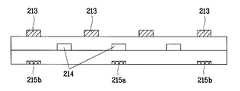
여기서, 도 4a에 도시한 바와 같이, 상기 데이터 배선 형성시, 이후 형성될 공통전극(213) 중 단위화소내의 가장 바깥쪽에 위치 할 공통전극의 하부에 차광층(215b)을 형성하고, 상기 단위화소내의 공통전극과 데이터전극의 광투과 영역이 동일하도록 단위화소 내의 데이터전극(214) 중 어느 하나의 데이터전극의 하부에 또다른 차광층(215a)을 형성한다.As shown in FIG. 4A, when the data line is formed, a
상기 데이터 배선은 구리(Cu), 알루미늄(Al), 크롬(Cr), 몰리브덴(Mo), 티타늄(Ti) 등의 빛을 차단하는 금속으로 형성하므로 공통전극의 하부 및 데이터전극의 하부에 형성되는 차광층들(215a,215b)을 형성하기 위한 별도의 추가공정은 필요하지 않다.The data line is formed of a metal that blocks light such as copper (Cu), aluminum (Al), chromium (Cr), molybdenum (Mo), and titanium (Ti), so that the data line is formed under the common electrode and under the data electrode. No additional process is required to form the
여기서, 상기에서와 같이 단위화소내의 가장 바깥쪽에 위치하는 공통전극을 차광하는 이유는 전압인가시 단위화소내의 양 끝쪽에서의 전계가 액정에 끼칠 영향이 불분명하기 때문인데, 상기와 같이 차광층을 형성하는 방법 이외에, 가장 바깥쪽에 위치하는 공통전극을 ITO가 아닌 빛을 차광할 수 있는 금속으로 형성하거나 제 2 기판의 블랙 매트릭스를 가장 바깥쪽에 위치하는 공통전극의 영역까지 연장하는 방법이 있다.The reason for shielding the common electrode located at the outermost side in the unit pixel as described above is that the effect of the electric fields at both ends of the unit pixel on the liquid crystal when the voltage is applied is unclear. In addition to the method, the outermost common electrode may be formed of a metal capable of shielding light other than ITO, or the black matrix of the second substrate may be extended to the region of the outermost common electrode.
이후, 상기 차광층(215a,215b)을 포함한 전면에 보호막을 형성한 다음, 상기 보호막 상에 상기 드레인 전극과 전기적으로 연결되며 상기 데이터 배선에 평행하도록 복수개의 데이터전극(214)을 형성하고, 상기 데이터전극(214)과 데이터전극 사이에 상응하는 위치에 복수개의 공통전극(213)을 형성한다.Subsequently, a passivation layer is formed on the entire surface including the
이때, 상기 공통전극(213)은 도 4b에서와 같이, 데이터 전극(214)의 하부에 형성할 수도 있으며, 도 4c에서와 같이, 데이터 전극(214)과 동일 평면상에 형성할 수도 있다. 참고적으로, 도 4b는 본 발명의 제 2 실시예에 따른 횡전계방식 액정표시장치의 요부 단면도이고, 도 4c는 본 발명의 제 3 실시예에 따른 요부 단면도이다.In this case, as shown in FIG. 4B, the
한편, 제 2 기판 상에는 빛의 누설을 방지하는 블랙 매트릭스를 형성하고, 상기 블랙 매트릭스 사이사이에 칼라필터층을 형성한다.Meanwhile, a black matrix is formed on the second substrate to prevent light leakage, and a color filter layer is formed between the black matrices.
마지막으로, 상기 제 1 기판과 제 2 기판을 대향 합착하고, 상기 두 기판 사이에 액정을 주입하여 횡전계방식 액정표시장치를 완성한다.Finally, the first substrate and the second substrate are opposed to each other, and a liquid crystal is injected between the two substrates to complete a transverse electric field type liquid crystal display device.
여기서, 상기 데이터전극(214) 및 공통전극(213)은 빛이 잘 투과되는 투명도전막인 ITO(Indium Tin Oxide)로 형성한다.The
이와 같은 본 발명의 횡전계방식 액정표시장치는 단위화소내 가장 바깥쪽에 위치하는 공통전극을 차광하더라도 데이터 전극을 통해 투과되는 광 투과면적과 공통전극을 통해 투과되는 광 투과면적이 동일하므로 DC전압을 인가할 경우 인가전압의 정(+), 부(-)에 따른 휘도차 발생을 방지한다.Such a transverse electric field type liquid crystal display device of the present invention has a DC voltage because the light transmitting area transmitted through the data electrode is the same as the light transmitting area transmitted through the common electrode even if the common electrode located at the outermost part of the unit pixel is shielded. When applied, the luminance difference caused by the positive (+) and negative (-) of the applied voltage is prevented.
한편, 본 발명의 제 4 실시예로서, 상기 단위 화소내 가장 바깥쪽에 위치한 공통전극을 투명도전막이 아닌 광을 차단할 수 있는 차광금속으로 형성하는 것이 가능하며, 차광금속으로 형성할 경우, 별도의 차광막을 형성한다거나 블랙 매트릭스를 연장할 필요가 없다.On the other hand, as a fourth embodiment of the present invention, it is possible to form the common electrode located on the outermost side of the unit pixel with a light shielding metal that can block light, not a transparent conductive film, and when formed with a light shielding metal, a separate light shielding film There is no need to form or extend the black matrix.
이와 같이, 본 발명의 제 1 실시예 내지 제 4 실시예는 단위 화소내 가장 바깥쪽에 위치하는 공통전극(213)을 차광할 경우에 발생하는 공통전극과 데이터 전극의 광 투과면적의 차이를 보상하기 위해 상기 데이터 전극(214) 중 적어도 어느 하나의 전극을 차광하여 단위 화소내에서 공통전극(213)과 데이터 전극(214)의 광 투과면적을 동일하게 한다(도 5 참조).As described above, the first to fourth embodiments of the present invention compensate for the difference between the light transmission areas of the common electrode and the data electrode generated when the
한편, 도 6a는 본 발명의 제 5 실시예에 따른 횡전계방식 액정표시장치의 요부 단면도이고, 도 6b는 본 발명의 제 6 실시예에 따른 요부 단면도이며, 도 6c는 본 발명의 제 7 실시예에 따른 요부 단면도로서, 상기 도 6a 내지 6c는 공통전극 중 적어도 어느 하나의 폭을 데이터 전극의 폭에 비해 넓게 패터닝 하였다.6A is a cross-sectional view illustrating main parts of a transverse electric field type liquid crystal display device according to a fifth embodiment of the present invention, FIG. 6B is a cross-sectional view of main parts according to a sixth embodiment of the present invention, and FIG. 6C is a seventh embodiment of the present invention. 6A through 6C illustrate a width of at least one of the common electrodes wider than the width of the data electrode.
즉, 본 발명의 제 1 내지 제 4 실시예는 단위 화소내 공통전극과 데이터 전극의 광 투과면적을 동일하게 하기 위해 데이터 전극중 어느 하나를 차광하였으나, 본 발명의 제 5 실시예 내지 제 7 실시예에서는 공통전극과 데이터 전극의 광 투과면적이 동일해지도록 적어도 어느 하나의 공통전극을 다른 데이터 전극에 비해 더 넓은 폭으로 형성하였다.That is, in the first to fourth embodiments of the present invention, any one of the data electrodes is shielded to make the same light transmitting area between the common electrode and the data electrode in the unit pixel, but the fifth to seventh embodiments of the present invention are performed. In the example, at least one common electrode is formed in a wider width than other data electrodes so that the light transmitting areas of the common electrode and the data electrode are the same.
이를 보다 상세하게 설명하면 다음과 같다.This will be described in more detail as follows.
도면에는 도시되지 않았지만, 제 1 기판 상에 금속을 증착하여 게이트 배선과, 상기 게이트 배선에서 분기되는 박막트랜지스터의 게이트전극을 패터닝한다.Although not shown in the figure, metal is deposited on the first substrate to pattern the gate wiring and the gate electrode of the thin film transistor branched from the gate wiring.
다음, 상기 게이트 배선을 포함한 전면에 게이트 절연막을 형성하고, 상기 게이트 절연막 상부에 상기 게이트 배선과 매트릭스 배열 구조를 이루어 단위화소 영역을 구분짓도록 데이터 배선을 형성한다.Next, a gate insulating film is formed on the entire surface including the gate wiring, and a data wiring is formed on the gate insulating film to form a matrix array structure to distinguish unit pixel regions.
이 때, 상기 데이터 배선과 동시에 박막트랜지스터 위치에 소스/드레인 전극을 형성한다.At this time, a source / drain electrode is formed at the thin film transistor position at the same time as the data line.
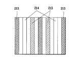
이어서, 도 6a에서와 같이 상기 데이터 배선 형성시, 이후 형성될 공통전극(313a,313b) 중 단위화소내의 가장 바깥쪽에 위치 할 공통전극의 하부에 상기 데이터 배선과 동일 물질로 차광층(315b)을 형성한 후, 상기 드레인 전극과 전기적으로 연결되며 상기 데이터 배선에 평행하도록 복수개의 데이터전극(314)을 형성하고, 상기 데이터전극(314)과 데이터전극 사이에 상응하는 위치에 복수개의 공통전극(313)을 형성하는데, 상기 복수개의 공통전극 중 적어도 어느 하나는 인접하는 데이터 전극의 폭에 비해 더 넓은 폭을 갖도록 형성한다.Subsequently, as shown in FIG. 6A, when the data line is formed, the
예를 들어 상기 공통전극과 데이터전극의 폭이 같고 데이터전극의 수가 공통전극의 수에 비해 하나 더 많다면, 공통전극 중 어느 하나의 공통전극의 폭을 2배로 형성함으로써, 공통전극과 데이터 전극의 광 투과면적을 동일하게 한다.For example, if the width of the common electrode and the data electrode is the same and the number of data electrodes is one more than the number of the common electrodes, the width of the common electrode and the data electrode may be doubled by forming twice the width of the common electrode of the common electrode. The light transmission area is made the same.
이때, 도 6a에서와 같이, 데이터 전극(314)을 포함한 전면에 절연막(325)을 형성하여 상기 절연막(325) 상에 공통전극(313a,313b)을 형성할 수도 있고, 도 6b에서와 같이, 공통전극(313a,313b)을 포함한 전면에 절연막(325)을 형성하여 상기 절연막(325)상에 데이터 전극(314)를 형성할 수도 있고, 도 6c에서와 같이, 공통전극(313a,313b)과 데이터 전극(314)를 동일 평면상에 형성할 수도 있다.In this case, as shown in FIG. 6A, common insulating
한편, 도면에는 도시하지 않았지만, 제 2 기판 상에는 빛의 누설을 방지하는 블랙 매트릭스을 형성하고, 상기 블랙 매트릭스 사이사이에 칼라필터층을 형성한다.On the other hand, although not shown in the figure, a black matrix is formed on the second substrate to prevent light leakage, and a color filter layer is formed between the black matrices.
이후 마지막으로, 상기 제 1 기판과 제 2 기판을 대향 합착하고, 상기 두 기판 사이에 액정을 주입하여 횡전계방식 액정표시장치를 완성한다.Then, finally, the first substrate and the second substrate are bonded to each other, and a liquid crystal is injected between the two substrates to complete a transverse electric field type liquid crystal display device.
여기서, 상기 데이터전극(314) 및 공통전극(313a,313b)은 ITO(Indium Tin Oxide)이며, 상기 도 6a 내지 도 6c에 도시된 공통전극 중 가장 바깥쪽에 위치한 공통전극(313a)만을 빛을 차단할 수 있는 차광금속으로 형성하는 것이 가능하다.The
이와 같이, 본 발명의 제 5 내지 제 7 실시예에서는 공통전극(313a,313b)과 데이터 전극(314)의 광 투과면적을 동일하게 하기 위해 어느 하나의 공통전극(313b)의 폭을 데이터 전극(314)의 폭에 비해 더 넓게 패터닝 하였다(도 7 참조).As described above, in the fifth to seventh exemplary embodiments of the present invention, the width of one
상기 공통전극의 폭을 더 넓게 패터닝 하는 이유는 단위 화소내에 형성된 복수개의 공통전극들 중 가장 바깥쪽에 위치한 공통전극을 차광함에 따라 차광되지 않는 공통전극의 면적이 데이터 전극의 면적에 비해 더 작기 때문에 상기 데이터 전극의 면적과 동일하게 해 주기 위함이다.
참고로, 본 발명에 의한 데이터 전극(314) 및 공통전극(313a,313b)은 도면에서와 같이, 스트라이프 타입으로 형성되는 이외에, 지그재그 타입으로 형성되어도 무방하다.The reason for patterning the width of the common electrode to be wider is that the area of the common electrode which is not shielded is smaller than that of the data electrode as the common electrode located at the outermost side among the plurality of common electrodes formed in the unit pixel is shielded. This is to make it equal to the area of the data electrode.
For reference, the
상기와 같은 본 발명의 횡전계방식 액정표시장치 및 그 제조방법은 다음과 같은 효과가 있다.As described above, the transverse electric field type liquid crystal display device and the method of manufacturing the same have the following effects.
첫째, 단위화소내 데이터전극과 공통전극의 광 투과영역을 동일하게 함으로서 DC전압을 인가할 경우 인가전압의 정부에 따른 휘도차를 없게 하여 휘도 차에 따른 플리커 및 잔상 문제를 개선한다.First, when the DC voltage is applied by making the light transmitting regions of the data electrode and the common electrode in the unit pixel the same, there is no luminance difference due to the government of the applied voltage, thereby improving the flicker and afterimage problems caused by the brightness difference.
둘째, 소정의 공통전극 및 데이터전극의 차광공정을 데이터 배선 형성공정과 동시에 하므로 공정을 간략화할 수 있고 그에 따른 공정시간을 최소화할 수 있다.Second, since the light shielding process of the predetermined common electrode and the data electrode is performed simultaneously with the data wiring forming process, the process can be simplified and the process time can be minimized.
Claims (19)
Translated fromKoreanPriority Applications (6)
| Application Number | Priority Date | Filing Date | Title |
|---|---|---|---|
| KR1020000061934AKR100587367B1 (en) | 2000-10-20 | 2000-10-20 | Transverse electric field liquid crystal display device and manufacturing method thereof |
| US09/892,879US6724454B2 (en) | 2000-10-20 | 2001-06-28 | Ips lcd device having a light shielding layer under at least one common or data electrodes so that light transmittance areas of the common and data electrodes are the same and a method of manufacturing the same |
| US10/777,852US7173682B2 (en) | 2000-10-20 | 2004-02-13 | In-plane switching mode liquid crystal display device and method of manufacturing the same |
| US11/647,285US7522245B2 (en) | 2000-10-20 | 2006-12-29 | In-plane switching mode liquid crystal display device |
| US12/382,559US8212984B2 (en) | 2000-10-20 | 2009-03-18 | Method of manufacturing an IPS LCD device having a light shielding layer under at least one common or data electrodes so that light transmittance areas of the common and data electrodes are the same |
| US13/494,621US8446553B2 (en) | 2000-10-20 | 2012-06-12 | In-plane switching mode liquid crystal display device and method of manufacturing the same |
Applications Claiming Priority (1)
| Application Number | Priority Date | Filing Date | Title |
|---|---|---|---|
| KR1020000061934AKR100587367B1 (en) | 2000-10-20 | 2000-10-20 | Transverse electric field liquid crystal display device and manufacturing method thereof |
Publications (2)
| Publication Number | Publication Date |
|---|---|
| KR20020031455A KR20020031455A (en) | 2002-05-02 |
| KR100587367B1true KR100587367B1 (en) | 2006-06-08 |
Family
ID=19694579
Family Applications (1)
| Application Number | Title | Priority Date | Filing Date |
|---|---|---|---|
| KR1020000061934AExpired - LifetimeKR100587367B1 (en) | 2000-10-20 | 2000-10-20 | Transverse electric field liquid crystal display device and manufacturing method thereof |
Country Status (2)
| Country | Link |
|---|---|
| US (5) | US6724454B2 (en) |
| KR (1) | KR100587367B1 (en) |
Cited By (1)
| Publication number | Priority date | Publication date | Assignee | Title |
|---|---|---|---|---|
| KR101419235B1 (en)* | 2007-12-26 | 2014-07-15 | 엘지디스플레이 주식회사 | Liquid Crystal Display Device and Method for Manufacturing the Same |
Families Citing this family (31)
| Publication number | Priority date | Publication date | Assignee | Title |
|---|---|---|---|---|
| DE60137091D1 (en)* | 2000-10-04 | 2009-01-29 | Panasonic Corp | Display control method |
| KR100587367B1 (en)* | 2000-10-20 | 2006-06-08 | 엘지.필립스 엘시디 주식회사 | Transverse electric field liquid crystal display device and manufacturing method thereof |
| KR100448047B1 (en)* | 2000-12-12 | 2004-09-10 | 비오이 하이디스 테크놀로지 주식회사 | Liquid crystal display for improving residual image |
| JP4085170B2 (en)* | 2002-06-06 | 2008-05-14 | 株式会社 日立ディスプレイズ | Liquid crystal display |
| US6765642B2 (en)* | 2002-09-18 | 2004-07-20 | Hannstar Display Corp. | In-plane switching liquid crystal display with a compensation electrode structure and method of forming the same |
| JP4344131B2 (en)* | 2002-12-19 | 2009-10-14 | 奇美電子股▲ふん▼有限公司 | Image display device |
| US7298445B1 (en) | 2003-06-23 | 2007-11-20 | Research Foundation Of The University Of Central Florida | Fast response liquid crystal mode |
| JP4385993B2 (en)* | 2005-05-10 | 2009-12-16 | 三菱電機株式会社 | Liquid crystal display device and manufacturing method thereof |
| KR101137840B1 (en)* | 2005-06-23 | 2012-04-20 | 엘지디스플레이 주식회사 | In-plane switching mode liquid crystal display device |
| US7932980B2 (en)* | 2005-11-23 | 2011-04-26 | University Of Central Florida Research Foundation, Inc. | Liquid crystal display device having patterned electrodes for repetitive divided horizontal electric field and fringing electric field |
| JP4717672B2 (en)* | 2006-03-17 | 2011-07-06 | ソニー株式会社 | Liquid crystal device and electronic device |
| JP5061505B2 (en)* | 2006-05-25 | 2012-10-31 | 日本電気株式会社 | Horizontal electric field type active matrix liquid crystal display device |
| US7369204B1 (en)* | 2006-07-21 | 2008-05-06 | Research Foundation Of The University Of Central Florida | Fast response liquid crystal mode |
| US7697093B2 (en)* | 2006-08-08 | 2010-04-13 | Au Optronics Corp. | Array panel |
| US7456475B2 (en)* | 2006-10-27 | 2008-11-25 | Hannstar Display Corp. | Display panel |
| TWI414864B (en)* | 2007-02-05 | 2013-11-11 | Hydis Tech Co Ltd | Fringe field switching mode lcd |
| KR20090049659A (en)* | 2007-11-14 | 2009-05-19 | 삼성전자주식회사 | Display substrate and display panel having same |
| KR101492106B1 (en)* | 2008-11-25 | 2015-02-11 | 삼성디스플레이 주식회사 | Liquid crystal display device and manufacturing method thereof |
| TWI749283B (en)* | 2008-11-28 | 2021-12-11 | 日商半導體能源研究所股份有限公司 | Liquid crystal display device |
| JP5425485B2 (en) | 2009-02-09 | 2014-02-26 | 株式会社ジャパンディスプレイ | Liquid crystal display |
| US9612489B2 (en)* | 2009-02-13 | 2017-04-04 | Apple Inc. | Placement and shape of electrodes for use in displays |
| KR101592011B1 (en)* | 2009-03-13 | 2016-02-05 | 삼성디스플레이 주식회사 | Liquid crystal display device |
| CN102116980B (en)* | 2009-12-31 | 2014-04-09 | 乐金显示有限公司 | Thin film transistor array substrate and method for fabricating same |
| JP5351118B2 (en)* | 2010-10-05 | 2013-11-27 | 株式会社ジャパンディスプレイ | Liquid crystal display |
| KR20120107721A (en)* | 2011-03-22 | 2012-10-04 | 삼성디스플레이 주식회사 | A fringe field switching mode liquid crystal display apparatus and an the manufacturing method thereof |
| KR102147520B1 (en) | 2013-07-29 | 2020-08-25 | 삼성디스플레이 주식회사 | Curved display apparatus |
| KR102140815B1 (en) | 2013-12-09 | 2020-08-04 | 삼성디스플레이 주식회사 | Liquid crystal display |
| KR102100263B1 (en)* | 2013-12-16 | 2020-04-13 | 엘지디스플레이 주식회사 | Array substrate for In-Plane switching mode liquid crystal display device |
| KR102426498B1 (en)* | 2015-12-24 | 2022-07-27 | 엘지디스플레이 주식회사 | Array Substrate For Touch Display Device And Method Of Fabricating The Same |
| KR102819878B1 (en)* | 2019-03-15 | 2025-06-12 | 삼성디스플레이 주식회사 | Display device |
| CN111308799B (en)* | 2019-11-13 | 2021-05-07 | Tcl华星光电技术有限公司 | Array substrate |
Citations (1)
| Publication number | Priority date | Publication date | Assignee | Title |
|---|---|---|---|---|
| JPH1062812A (en)* | 1996-08-20 | 1998-03-06 | Nec Corp | Liquid crystal display device |
Family Cites Families (33)
| Publication number | Priority date | Publication date | Assignee | Title |
|---|---|---|---|---|
| US5162933A (en)* | 1990-05-16 | 1992-11-10 | Nippon Telegraph And Telephone Corporation | Active matrix structure for liquid crystal display elements wherein each of the gate/data lines includes at least a molybdenum-base alloy layer containing 0.5 to 10 wt. % of chromium |
| EP0588568B1 (en) | 1992-09-18 | 2002-12-18 | Hitachi, Ltd. | A liquid crystal display device |
| JPH095764A (en) | 1995-06-20 | 1997-01-10 | Hitachi Ltd | LCD display substrate |
| JP3474975B2 (en) | 1995-09-06 | 2003-12-08 | 株式会社 日立ディスプレイズ | Liquid crystal display device and method of manufacturing the same |
| JP3632934B2 (en) | 1995-10-04 | 2005-03-30 | 株式会社 日立ディスプレイズ | Active matrix liquid crystal display device |
| JPH09105908A (en) | 1995-10-09 | 1997-04-22 | Hitachi Ltd | Active matrix type liquid crystal display |
| TW454101B (en) | 1995-10-04 | 2001-09-11 | Hitachi Ltd | In-plane field type liquid crystal display device comprising liquid crystal molecules with more than two different kinds of reorientation directions and its manufacturing method |
| US5745207A (en) | 1995-11-30 | 1998-04-28 | Matsushita Electric Industrial Co., Ltd. | Active matrix liquid crystal display having electric fields parallel to substrates |
| JP3396130B2 (en) | 1996-06-03 | 2003-04-14 | シャープ株式会社 | Liquid crystal display |
| JP2973934B2 (en) | 1996-07-11 | 1999-11-08 | 日本電気株式会社 | Liquid crystal display device and electronic equipment equipped with liquid crystal display device |
| KR100258435B1 (en)* | 1996-10-22 | 2000-06-01 | 윤종용 | A substrate for liquid crystal display of in-plane switching mode |
| US5907379A (en)* | 1996-10-21 | 1999-05-25 | Samsung Electronics Co., Ltd. | In-plane switching liquid crystal display having high aperture ratio |
| TW396289B (en)* | 1996-10-29 | 2000-07-01 | Nippon Electric Co | Liquid crystal display device |
| JP3883244B2 (en)* | 1997-01-23 | 2007-02-21 | エルジー フィリップス エルシーディー カンパニー リミテッド | Liquid crystal display |
| KR100257369B1 (en)* | 1997-05-19 | 2000-05-15 | 구본준 | In plane switching mode liquid crystal display device |
| KR100262405B1 (en) | 1997-06-27 | 2000-08-01 | 김영환 | Liquid crystal display element |
| JP4130490B2 (en)* | 1997-10-16 | 2008-08-06 | 三菱電機株式会社 | Liquid crystal display |
| US6133977A (en)* | 1997-10-21 | 2000-10-17 | Samsung Electronics Co., Ltd. | Liquid crystal displays having common electrode overlap with one or more data lines |
| JP3031317B2 (en)* | 1997-11-20 | 2000-04-10 | 日本電気株式会社 | Active matrix liquid crystal display |
| KR100375732B1 (en)* | 1997-11-25 | 2004-10-14 | 비오이 하이디스 테크놀로지 주식회사 | LCD Display |
| KR100482458B1 (en)* | 1997-12-08 | 2005-08-10 | 비오이 하이디스 테크놀로지 주식회사 | Thin film transistor liquid crystal display device and manufacturing method |
| WO1999031545A1 (en)* | 1997-12-17 | 1999-06-24 | Matsushita Electric Industrial Co., Ltd. | Polymer dispersion type liquid crystal display panel and its manufacturing method |
| KR100293436B1 (en)* | 1998-01-23 | 2001-08-07 | 구본준, 론 위라하디락사 | In plane switching mode liquid crystal display device |
| JP3042491B2 (en) | 1998-03-20 | 2000-05-15 | 日本電気株式会社 | Liquid crystal display panel and liquid crystal display device |
| JP3099812B2 (en)* | 1998-07-30 | 2000-10-16 | 日本電気株式会社 | Liquid crystal display |
| KR100299381B1 (en)* | 1998-08-24 | 2002-06-20 | 박종섭 | Liquid crystal display device having high opening ratio and high transmittance and manufacturing method thereof |
| KR100320416B1 (en)* | 1998-08-26 | 2002-09-17 | 엘지.필립스 엘시디 주식회사 | In-plane switching mode liquid crystal display device |
| KR20000027768A (en)* | 1998-10-29 | 2000-05-15 | 김영환 | Lcd with high aperture rate and high transmissivity |
| TWI251697B (en)* | 1999-05-26 | 2006-03-21 | Matsushita Electric Industrial Co Ltd | Liquid crystal display element and producing method thereof |
| JP3481509B2 (en)* | 1999-06-16 | 2003-12-22 | Nec液晶テクノロジー株式会社 | Liquid crystal display |
| KR100433596B1 (en)* | 1999-10-21 | 2004-05-31 | 마쯔시다덴기산교 가부시키가이샤 | Liquid crystal device |
| JP2001249349A (en)* | 2000-03-02 | 2001-09-14 | Mitsubishi Electric Corp | Liquid crystal display |
| KR100587367B1 (en)* | 2000-10-20 | 2006-06-08 | 엘지.필립스 엘시디 주식회사 | Transverse electric field liquid crystal display device and manufacturing method thereof |
- 2000
- 2000-10-20KRKR1020000061934Apatent/KR100587367B1/ennot_activeExpired - Lifetime
- 2001
- 2001-06-28USUS09/892,879patent/US6724454B2/ennot_activeExpired - Lifetime
- 2004
- 2004-02-13USUS10/777,852patent/US7173682B2/ennot_activeExpired - Lifetime
- 2006
- 2006-12-29USUS11/647,285patent/US7522245B2/ennot_activeExpired - Lifetime
- 2009
- 2009-03-18USUS12/382,559patent/US8212984B2/ennot_activeExpired - Fee Related
- 2012
- 2012-06-12USUS13/494,621patent/US8446553B2/ennot_activeExpired - Fee Related
Patent Citations (1)
| Publication number | Priority date | Publication date | Assignee | Title |
|---|---|---|---|---|
| JPH1062812A (en)* | 1996-08-20 | 1998-03-06 | Nec Corp | Liquid crystal display device |
Cited By (1)
| Publication number | Priority date | Publication date | Assignee | Title |
|---|---|---|---|---|
| KR101419235B1 (en)* | 2007-12-26 | 2014-07-15 | 엘지디스플레이 주식회사 | Liquid Crystal Display Device and Method for Manufacturing the Same |
Also Published As
| Publication number | Publication date |
|---|---|
| US20040218131A1 (en) | 2004-11-04 |
| US20090186551A1 (en) | 2009-07-23 |
| KR20020031455A (en) | 2002-05-02 |
| US8446553B2 (en) | 2013-05-21 |
| US8212984B2 (en) | 2012-07-03 |
| US7173682B2 (en) | 2007-02-06 |
| US20070109479A1 (en) | 2007-05-17 |
| US6724454B2 (en) | 2004-04-20 |
| US20020047972A1 (en) | 2002-04-25 |
| US7522245B2 (en) | 2009-04-21 |
| US20120264242A1 (en) | 2012-10-18 |
Similar Documents
| Publication | Publication Date | Title |
|---|---|---|
| KR100587367B1 (en) | Transverse electric field liquid crystal display device and manufacturing method thereof | |
| KR100730495B1 (en) | Transverse electric field type liquid crystal display device and manufacturing method thereof | |
| US8614779B2 (en) | Lateral electric field type active-matrix addressing liquid crystal display device | |
| KR101112537B1 (en) | Liquid crystal display having multi domain and panel for the same | |
| KR101182471B1 (en) | Fringe field switching mode liquid crystal display device and manufacturing method thereof | |
| US8072569B2 (en) | Fringe field switching liquid crystal display panel | |
| US20070229749A1 (en) | FFS mode liquid crystal display panel | |
| KR100689312B1 (en) | Horizontal field type liquid crystal display device and manufacturing method thereof | |
| JP2005512153A (en) | High aperture ratio LCD | |
| JP3006586B2 (en) | Active matrix type liquid crystal display | |
| KR20060001662A (en) | Horizontal field type liquid crystal display device and manufacturing method thereof | |
| KR20050039554A (en) | Ips liquid crystal display device | |
| KR101247698B1 (en) | Liquid crystal display | |
| KR101016525B1 (en) | Horizontal field type liquid crystal display device | |
| KR20080030244A (en) | Liquid crystal display | |
| JP4407677B2 (en) | Horizontal electric field LCD panel | |
| KR20080046042A (en) | Display panel | |
| JP2004258652A (en) | Liquid crystal display | |
| JP2005182048A (en) | Multi-domain thin film transistor array panel and liquid crystal display device including the same | |
| KR20090084176A (en) | LCD Display | |
| JP3282542B2 (en) | Active matrix type liquid crystal display | |
| KR100652219B1 (en) | Transverse electric field liquid crystal display device | |
| KR100361333B1 (en) | Liquid crystal display | |
| KR20020037554A (en) | IPS mode Liquid crystal display device and method for fabricating the same | |
| KR20050063006A (en) | In plane switching mode liquid crystal display device and method for fabricating thereof |
Legal Events
| Date | Code | Title | Description |
|---|---|---|---|
| PA0109 | Patent application | Patent event code:PA01091R01D Comment text:Patent Application Patent event date:20001020 | |
| PG1501 | Laying open of application | ||
| A201 | Request for examination | ||
| PA0201 | Request for examination | Patent event code:PA02012R01D Patent event date:20040120 Comment text:Request for Examination of Application Patent event code:PA02011R01I Patent event date:20001020 Comment text:Patent Application | |
| E902 | Notification of reason for refusal | ||
| PE0902 | Notice of grounds for rejection | Comment text:Notification of reason for refusal Patent event date:20051118 Patent event code:PE09021S01D | |
| E701 | Decision to grant or registration of patent right | ||
| PE0701 | Decision of registration | Patent event code:PE07011S01D Comment text:Decision to Grant Registration Patent event date:20060412 | |
| GRNT | Written decision to grant | ||
| PR0701 | Registration of establishment | Comment text:Registration of Establishment Patent event date:20060530 Patent event code:PR07011E01D | |
| PR1002 | Payment of registration fee | Payment date:20060601 End annual number:3 Start annual number:1 | |
| PG1601 | Publication of registration | ||
| PR1001 | Payment of annual fee | Payment date:20090323 Start annual number:4 End annual number:4 | |
| PR1001 | Payment of annual fee | Payment date:20100318 Start annual number:5 End annual number:5 | |
| PR1001 | Payment of annual fee | Payment date:20110329 Start annual number:6 End annual number:6 | |
| FPAY | Annual fee payment | ||
| PR1001 | Payment of annual fee | Payment date:20120330 Start annual number:7 End annual number:7 | |
| FPAY | Annual fee payment | ||
| PR1001 | Payment of annual fee | Payment date:20130329 Start annual number:8 End annual number:8 | |
| PR1001 | Payment of annual fee | Payment date:20140328 Start annual number:9 End annual number:9 | |
| FPAY | Annual fee payment | Payment date:20150429 Year of fee payment:10 | |
| PR1001 | Payment of annual fee | Payment date:20150429 Start annual number:10 End annual number:10 | |
| FPAY | Annual fee payment | Payment date:20160428 Year of fee payment:11 | |
| PR1001 | Payment of annual fee | Payment date:20160428 Start annual number:11 End annual number:11 | |
| FPAY | Annual fee payment | Payment date:20170413 Year of fee payment:12 | |
| PR1001 | Payment of annual fee | Payment date:20170413 Start annual number:12 End annual number:12 | |
| FPAY | Annual fee payment | Payment date:20180416 Year of fee payment:13 | |
| PR1001 | Payment of annual fee | Payment date:20180416 Start annual number:13 End annual number:13 | |
| FPAY | Annual fee payment | Payment date:20190417 Year of fee payment:14 | |
| PR1001 | Payment of annual fee | Payment date:20190417 Start annual number:14 End annual number:14 | |
| PR1001 | Payment of annual fee | Payment date:20200422 Start annual number:15 End annual number:15 | |
| PC1801 | Expiration of term |