KR100587340B1 - Manufacturing method of organic EL element - Google Patents
Manufacturing method of organic EL elementDownload PDFInfo
- Publication number
- KR100587340B1 KR100587340B1KR1020030090167AKR20030090167AKR100587340B1KR 100587340 B1KR100587340 B1KR 100587340B1KR 1020030090167 AKR1020030090167 AKR 1020030090167AKR 20030090167 AKR20030090167 AKR 20030090167AKR 100587340 B1KR100587340 B1KR 100587340B1
- Authority
- KR
- South Korea
- Prior art keywords
- organic
- anode electrode
- forming
- partition wall
- manufacturing
- Prior art date
- Legal status (The legal status is an assumption and is not a legal conclusion. Google has not performed a legal analysis and makes no representation as to the accuracy of the status listed.)
- Expired - Lifetime
Links
- 238000004519manufacturing processMethods0.000titleclaimsabstractdescription24
- 238000000034methodMethods0.000claimsabstractdescription32
- 238000005192partitionMethods0.000claimsabstractdescription23
- 239000000758substrateSubstances0.000claimsdescription15
- 239000007772electrode materialSubstances0.000claimsdescription10
- 229910052751metalInorganic materials0.000claimsdescription7
- 239000002184metalSubstances0.000claimsdescription7
- 238000000151depositionMethods0.000claimsdescription4
- 229910010272inorganic materialInorganic materials0.000claimsdescription3
- 239000011147inorganic materialSubstances0.000claimsdescription3
- 239000000203mixtureSubstances0.000claimsdescription3
- 239000011368organic materialSubstances0.000claimsdescription3
- 238000010030laminatingMethods0.000claimsdescription2
- 230000000149penetrating effectEffects0.000claimsdescription2
- 230000008569processEffects0.000abstractdescription17
- 229920002120photoresistant polymerPolymers0.000abstractdescription13
- 239000010408filmSubstances0.000description57
- 239000004065semiconductorSubstances0.000description11
- 238000005530etchingMethods0.000description7
- 239000000463materialSubstances0.000description7
- 239000011159matrix materialSubstances0.000description7
- 239000011651chromiumSubstances0.000description5
- 229910021417amorphous siliconInorganic materials0.000description4
- 239000012535impuritySubstances0.000description4
- 239000012212insulatorSubstances0.000description4
- 229910021420polycrystalline siliconInorganic materials0.000description4
- 239000010409thin filmSubstances0.000description4
- 230000008901benefitEffects0.000description3
- 229910052804chromiumInorganic materials0.000description3
- 238000010586diagramMethods0.000description3
- VYZAMTAEIAYCRO-UHFFFAOYSA-NChromiumChemical compound[Cr]VYZAMTAEIAYCRO-UHFFFAOYSA-N0.000description2
- XUIMIQQOPSSXEZ-UHFFFAOYSA-NSiliconChemical compound[Si]XUIMIQQOPSSXEZ-UHFFFAOYSA-N0.000description2
- 230000004888barrier functionEffects0.000description2
- 239000011521glassSubstances0.000description2
- 238000010438heat treatmentMethods0.000description2
- 230000001678irradiating effectEffects0.000description2
- 150000002739metalsChemical class0.000description2
- 229920005591polysiliconPolymers0.000description2
- 238000000926separation methodMethods0.000description2
- 229910052710siliconInorganic materials0.000description2
- 239000010703siliconSubstances0.000description2
- 239000004642PolyimideSubstances0.000description1
- 229910045601alloyInorganic materials0.000description1
- 239000000956alloySubstances0.000description1
- 229910052782aluminiumInorganic materials0.000description1
- 239000003990capacitorSubstances0.000description1
- 238000000576coating methodMethods0.000description1
- 239000004020conductorSubstances0.000description1
- 238000007796conventional methodMethods0.000description1
- 229910052802copperInorganic materials0.000description1
- 230000007423decreaseEffects0.000description1
- 230000008021depositionEffects0.000description1
- 230000000694effectsEffects0.000description1
- 230000005281excited stateEffects0.000description1
- 229910052737goldInorganic materials0.000description1
- 230000005283ground stateEffects0.000description1
- 238000002347injectionMethods0.000description1
- 239000007924injectionSubstances0.000description1
- 239000004973liquid crystal related substanceSubstances0.000description1
- 238000012986modificationMethods0.000description1
- 230000004048modificationEffects0.000description1
- 229910052759nickelInorganic materials0.000description1
- 229920003986novolacPolymers0.000description1
- 239000004033plasticSubstances0.000description1
- 229920001721polyimidePolymers0.000description1
- 230000004044responseEffects0.000description1
- 229910052709silverInorganic materials0.000description1
- 238000003860storageMethods0.000description1
- 229910052715tantalumInorganic materials0.000description1
- 229910052719titaniumInorganic materials0.000description1
- 229910052721tungstenInorganic materials0.000description1
Images


Classifications
- H—ELECTRICITY
- H10—SEMICONDUCTOR DEVICES; ELECTRIC SOLID-STATE DEVICES NOT OTHERWISE PROVIDED FOR
- H10K—ORGANIC ELECTRIC SOLID-STATE DEVICES
- H10K59/00—Integrated devices, or assemblies of multiple devices, comprising at least one organic light-emitting element covered by group H10K50/00
- H10K59/10—OLED displays
- H10K59/12—Active-matrix OLED [AMOLED] displays
- H10K59/122—Pixel-defining structures or layers, e.g. banks
- H—ELECTRICITY
- H05—ELECTRIC TECHNIQUES NOT OTHERWISE PROVIDED FOR
- H05B—ELECTRIC HEATING; ELECTRIC LIGHT SOURCES NOT OTHERWISE PROVIDED FOR; CIRCUIT ARRANGEMENTS FOR ELECTRIC LIGHT SOURCES, IN GENERAL
- H05B33/00—Electroluminescent light sources
- H05B33/10—Apparatus or processes specially adapted to the manufacture of electroluminescent light sources
- H—ELECTRICITY
- H10—SEMICONDUCTOR DEVICES; ELECTRIC SOLID-STATE DEVICES NOT OTHERWISE PROVIDED FOR
- H10K—ORGANIC ELECTRIC SOLID-STATE DEVICES
- H10K50/00—Organic light-emitting devices
- H10K50/80—Constructional details
- H10K50/805—Electrodes
- H10K50/81—Anodes
- H10K50/818—Reflective anodes, e.g. ITO combined with thick metallic layers
- H—ELECTRICITY
- H10—SEMICONDUCTOR DEVICES; ELECTRIC SOLID-STATE DEVICES NOT OTHERWISE PROVIDED FOR
- H10K—ORGANIC ELECTRIC SOLID-STATE DEVICES
- H10K59/00—Integrated devices, or assemblies of multiple devices, comprising at least one organic light-emitting element covered by group H10K50/00
- H10K59/80—Constructional details
- H10K59/805—Electrodes
- H10K59/8051—Anodes
- H10K59/80518—Reflective anodes, e.g. ITO combined with thick metallic layers
- H—ELECTRICITY
- H10—SEMICONDUCTOR DEVICES; ELECTRIC SOLID-STATE DEVICES NOT OTHERWISE PROVIDED FOR
- H10K—ORGANIC ELECTRIC SOLID-STATE DEVICES
- H10K2102/00—Constructional details relating to the organic devices covered by this subclass
- H10K2102/301—Details of OLEDs
- H10K2102/302—Details of OLEDs of OLED structures
- H10K2102/3023—Direction of light emission
- H10K2102/3026—Top emission
- Y—GENERAL TAGGING OF NEW TECHNOLOGICAL DEVELOPMENTS; GENERAL TAGGING OF CROSS-SECTIONAL TECHNOLOGIES SPANNING OVER SEVERAL SECTIONS OF THE IPC; TECHNICAL SUBJECTS COVERED BY FORMER USPC CROSS-REFERENCE ART COLLECTIONS [XRACs] AND DIGESTS
- Y10—TECHNICAL SUBJECTS COVERED BY FORMER USPC
- Y10S—TECHNICAL SUBJECTS COVERED BY FORMER USPC CROSS-REFERENCE ART COLLECTIONS [XRACs] AND DIGESTS
- Y10S428/00—Stock material or miscellaneous articles
- Y10S428/917—Electroluminescent
Landscapes
- Engineering & Computer Science (AREA)
- Microelectronics & Electronic Packaging (AREA)
- Manufacturing & Machinery (AREA)
- Physics & Mathematics (AREA)
- Optics & Photonics (AREA)
- Electroluminescent Light Sources (AREA)
Abstract
Translated fromKoreanDescription
Translated fromKorean도 1a 내지 도 1f는 종래 기술에 따른 유기 EL 소자의 제조공정 단면도1A to 1F are cross-sectional views of a manufacturing process of an organic EL device according to the prior art.
도 2a 내지 도 2d는 종래 기술에 따른 유기 EL 소자 제조시에 발생될 수 있는 문제점을 설명하기 위한 도면2A to 2D are diagrams for explaining a problem that may occur when manufacturing an organic EL device according to the prior art.
도 3a 내지 3e는 본 발명에 따른 유기 EL 소자의 제조 공정에 따른 평면도3A to 3E are plan views of the manufacturing process of the organic EL device according to the present invention.
도 4a 내지 도 4e는 각각 도 2a 내지 도 3e 공정에서의 A-A 방향 단면도4A-4E are cross-sectional views along the A-A direction in the processes of FIGS. 2A-3E, respectively.
도 5a 내지 도 5e는 본 발명에 따른 격벽 구조를 예시한 도면5A to 5E are diagrams illustrating a partition structure according to the present invention.
**도면의 주요 부분에 대한 부호 설명**** Description of the symbols for the main parts of the drawings **
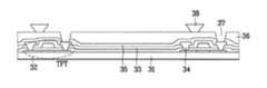
31 : 투명 기판 32 : TFT31
33 : 제 1 절연막 34 : 콘택33: first insulating film 34: contact
35 : 제 2 절연막 36 : 평탄화 절연막35 second
37 : 비아홀 38 : 격벽37: via hole 38: bulkhead
39 : 어노드 전극 40 : 절연막39: anode electrode 40: insulating film
본 발명은 평면표시소자에 관한 것으로 특히, 소자의 신뢰성을 향상시키고, 제조 공정을 단순화키기에 적합한 유기 EL 소자의 제조방법에 관한 것이다.BACKGROUND OF THE INVENTION 1. Field of the Invention The present invention relates to flat panel display devices, and more particularly, to a method for manufacturing an organic EL device suitable for improving the reliability of the device and simplifying the manufacturing process.
최근, 표시장치의 대형화에 따라 공간 점유가 적은 평면표시소자의 요구가 증대되고 있는데, 이러한 평면표시소자 중 하나로서 유기발광다이오드(Organic Light Emitting Diode : OLED)라고도 불리는 유기 전계발광소자의 기술이 빠른 속도로 발전하고 있으며, 이미 여러 시제품들이 발표된 바 있다.Recently, as the size of the display device increases, the demand for a flat display device having less space is increasing. As one of the flat display devices, an organic light emitting diode (OLED), which is also called an organic light emitting diode (OLED), has been rapidly developed. It is evolving at a rate, and several prototypes have already been announced.
유기 전계발광소자는 전자주입전극(Cathode)인 제 1 전극과, 정공주입전극(Anode)인 제 2 전극 사이에 형성된 유기 발광층에 각각 전자와 정공을 주입하면 전자와 정공이 결합하여 쌍을 이루어 생성된 액시톤(Exciton)이 여기 상태로부터 기저상태로 떨어지면서 소멸하여 발광하는 소자이다.An organic electroluminescent device is formed by pairing electrons and holes by injecting electrons and holes into an organic light emitting layer formed between a first electrode, which is an electron injection electrode, and a second electrode, which is an anode. Exciton is an element that is extinguished and emits light while falling from the excited state to the ground state.
이러한 유기 전계발광소자는 플라즈마 디스플레이 패널(Plasma Display Panel : PDP)이나 무기 전계발광소자 디스플레이에 비해 낮은 전압(5~10V)으로 구동할 수 있다는 장점이 있어 연구가 활발히 진행되고 있다.Such organic electroluminescent devices have the advantage that they can be driven at a lower voltage (5-10V) than plasma display panels (PDPs) or inorganic electroluminescent device displays.
그리고, 유기 전계발광소자는 넓은 시야각, 고속 응답성, 고 콘트라스트(Contrast) 등의 뛰어난 특징을 갖고 있으므로, 그래픽 디스플레이의 픽셀(Pixel), 텔레비전 영상 디스플레이나 표면광원(Surface Light Source)의 픽셀로서 사용될 수 있으며, 플라스틱 같이 휠 수 있는(Flexible) 투명 기판상에도 소자를 형성할 수 있고, 매우 얇고 가볍게 만들 수 있으며, 색감이 좋기 때문에 차세대 평면 디스플레이(Flat Panel Display : FPD)에 적합한 소자이다.In addition, organic electroluminescent devices have excellent characteristics such as wide viewing angle, high-speed response, and high contrast, so that they can be used as pixels of graphic displays, pixels of television image displays, or surface light sources. In addition, the device can be formed on a flexible transparent substrate, such as plastic, can be made very thin and light, and has good color, which is suitable for a next-generation flat panel display (FPD).
또한, 이미 잘 알려진 액정표시장치(Liquid Crystal Display : LCD)에 비해 백라이트(Backlight)가 필요치 않아 전력소비가 적고 색감이 뛰어나다는 장점도 있다.In addition, compared to the well-known liquid crystal display (LCD), it does not require a backlight, so there is an advantage of low power consumption and excellent color.
일반적으로, 유기 전계 발광소자는 그 구조 및 구동방법에 있어 크게 패시브(Passive) 매트릭스와 액티브(Active) 매트릭스로 구분된다.In general, organic EL devices are classified into a passive matrix and an active matrix in their structure and driving method.
상기 액티브 매트릭스는 패시브 매트릭스와는 달리 글라스(Glass)면으로 발광시키는 경우(통상, 바텀 이미션(Bottom Emission)이라 함) TFT(Thin Film Transistor)의 크기나 수가 많아질수록 개구율이 기하급수적으로 줄어들어 디스플레이 소자로서의 사용이 어렵게 된다.Unlike the passive matrix, when the active matrix emits light on a glass surface (commonly referred to as bottom emission), as the size or number of TFTs (thin film transistors) increases, the aperture ratio decreases exponentially. It becomes difficult to use as a display element.
이러한 문제점을 극복하기 위하여 개구율이 상기 TFT와 상관성을 갖지 않도록 글라스 반대면으로 발광시키는 탑 이미션(Top Emission) 방식이 대두되었다.In order to overcome this problem, a top emission method that emits light toward the glass opposite surface has been introduced so that the aperture ratio does not have correlation with the TFT.
탑 이미션 방식의 유기 전계 발광 소자는 TFT 및 저장 커패시터를 포함하는 기판과, 기판상에 형성되는 반사층, 상기 반사층상에 차례로 형성되는 유기 발광층과 투명 전극층을 포함하여 구성되어, 상기 유기 발광층에서의 발광이 상기 반사층에 부딪혀 기판면의 반대쪽으로 이루어진다. 때문에 상기 TFT에 의한 개구율 저하가 발생되지 않는다.The top emission type organic electroluminescent device includes a substrate including a TFT and a storage capacitor, a reflective layer formed on the substrate, an organic light emitting layer formed on the reflective layer, and a transparent electrode layer. Light emission impinges on the reflective layer and is opposite to the substrate surface. Therefore, the opening ratio fall by the TFT does not occur.
이하, 첨부된 도면을 참조하여 종래 기술에 따른 탑 이미션 방식의 액티브 매트릭스 유기 EL 소자의 제조 방법을 설명하면 다음과 같다.Hereinafter, a method of manufacturing a top emission type active matrix organic EL device according to the prior art will be described with reference to the accompanying drawings.
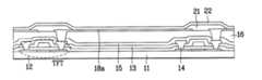
도 1a 내지 도 1f는 종래 기술에 따른 종래 기술에 따른 탑 이미션 방식의 액티브 매트릭스 유기 EL 소자의 제조공정 단면도이다.1A to 1F are cross-sectional views of a process of manufacturing an active matrix organic EL device having a top emission method according to the prior art according to the prior art.
먼저, 도 1a에 도시된 바와 같이 투명 기판(11)상에 픽셀 단위로 TFT(Thin Film Transistor)(12)를 형성한다.First, as illustrated in FIG. 1A, a thin film transistor (TFT) 12 is formed on a
즉, 투명 기판(11)상에 비정질 실리콘(amorphous silicon)을 형성하고, 비정질 실리콘의 표면에 레이저를 조사함으로써 비정질 실리콘을 용융 재결정화하여 다결정 실리콘(poly Silicon)막을 형성한 다음에 포토 및 식각 공정으로 상기 다결정 실리콘막을 섬 형상으로 패터닝하여 반도체막(12a)을 형성하고, 반도체막(12a)을 포함한 전면에 게이트 절연막(12b)을 형성하고, 게이트 절연막(12b)상에 예를 들어 크롬(Cr)으로 이루어진 금속막을 형성한 후 포토 및 식각 공정으로 게이트 절연막(12b)상의 반도체막(12a)의 중앙 부분에 대응하여 중첩되는 위치에 게이트 전극(12c)을 형성한다.That is, the amorphous silicon is formed on the
그 다음, 상기 게이트 전극(12c)을 마스크로 상기 반도체막(12a)에 대하여 p형 또는 n형의 불순물을 주입하고, 주입된 불순물을 활성화시키기 위해서 가열 처리를 실시하여, 반도체막(12a)에 소오스 영역(12d) 및 드레인 영역(12e)을 형성한다.Subsequently, a p-type or n-type impurity is implanted into the
이렇게 해서, TFT(12)를 완성한다.In this way, the TFT 12 is completed.
이어, 상기 TFT(12)를 포함한 전면에 제 1 절연막(13)을 형성하고, 상기 제 1 절연막(13)과 게이트 절연막(12b)을 관통하여 TFT(12)의 소오스 전극(12d) 및 드레인 전극(12e)에 각각 연결되는 콘택(14)을 형성하고, 전면에 제 2 절연막(15)을 형성한다.Subsequently, a first
이어, 도 1b에 도시된 바와 같이 상기 제 2 절연막(15)상에 평탄화 절연막(16)을 형성하고, 포토 및 식각 공정으로 상기 드레인 전극(12e)에 연결되는 콘택(14) 표면이 노출되도록 상기 평탄화 절연막(16) 및 제 2 절연막(15)을 선택적으로 제거하여 비아홀(Via-hole)(17)을 형성한다.Subsequently, as shown in FIG. 1B, the
이어서, 도 1c에 도시된 바와 같이 상기 비아홀(17)이 매립될 수 있도록 상기 비아홀(17)을 포함한 평탄화 절연막(16)상에 어노드(anode) 전극용 물질(18)을 증착한다.Subsequently, an
이어, 도 1d에 도시된 비와 같이 어노드 전극이 픽셀 단위로 분리될 수 있도록 포토 및 식각 공정으로 상기 어노드 전극용 물질(18)을 선택적으로 제거하여 어노드 전극(18a)을 형성하고, 발광부를 제외한 부분에 절연막(21)을 형성한다.Subsequently, as shown in FIG. 1D, the
그 다음에 도 1e에 도시된 바와 같이, 전면에 유기 EL층(22)을 형성하고 이어서, 도 1f에 도시된 바와 같이 상기 유기 EL층(22)상에 캐소드 전극(23)을 형성한다.Then, as shown in Fig. 1E, an
이로써, 종래 기술에 따른 탑-이미션 방식의 액티브 매트릭스 유기 EL 소자를 완성한다.This completes the active matrix organic EL device of the top emission method according to the prior art.
그런데, 상기 어노드 전극(18a)과 평탄화 절연막(16)간은 접착력이 좋이 않다. 때문에, 상기 어노드 전극을 분리하기 위한 포토 및 식각 공정에서 사용된 포토레지스트를 제거할 때, 어노드 전극(18a)이 평탄화 절연막(16)으로부터 박리되는 현상이 함께 발생될 우려가 크다.However, the adhesion between the
이와 같은 종래 기술에 따른 문제점을 첨부된 도면을 참조하여 보다 상세히 살펴보면 다음과 같다.Looking at the problem according to the prior art in more detail with reference to the accompanying drawings as follows.
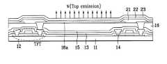
도 2a 내지 도 2d는 종래 기술에 따른 유기 EL 소자 제조시에 발생될 수 있 는 문제점을 설명하기 위한 도면이다.2A to 2D are diagrams for explaining a problem that may occur when manufacturing an organic EL device according to the prior art.
상기 도 1c에서와 같이 어노드 전극용 물질(18) 증착을 완료한 다음에 어노드 전극이 픽셀 단위로 분리될 수 있도록 포토 및 식각 공정을 진행해야 한다.As shown in FIG. 1C, after the deposition of the material for the
즉, 도 2a에 도시된 바와 같이 상기 어노드 전극용 물질(18)상에 포토레지스트(19)를 도포하고 픽셀의 가장자리 부분을 노출하도록 패터닝된 마스크(20)를 투명 기판(11)상에 얼라인시킨 다음, 상기 마스크(20) 위에서 투명 기판(11)을 향해 빛을 조사하여 상기 포토레지스트(19)를 노광시킨다.That is, as shown in FIG. 2A, the
이어, 상기 마스크(20)를 제거하고 상기 포토레지스트(19)를 현상하면 도 2b에 도시된 바와 같이, 포토레지스트(19)의 노광된 부위가 제거되게 되게 된다.Subsequently, when the
이어, 도 2c에 도시된 바와 같이, 상기 포토레지스트(19)를 마스크로 어노드 전극용 물질(18)을 제거하여 픽셀 단위로 어노드 전극(18a)을 형성한 다음에 상기 투명 기판(11)을 스트립퍼(stripper)에 넣어 도 2d에 도시된 바와 같이 포토레지스트(19)를 제거한다.Subsequently, as shown in FIG. 2C, the
이때, 상기 평탄화 절연막(16)과 어노드 전극(18a)간의 접착력(adhesion)이 좋지 않음으로 인하여 어노드 전극(18a)이 평탄화 절연막(16)으로부터 박리되는 현상이 발생되게 된다.At this time, due to the poor adhesion between the
따라서, 소자의 신뢰성이 크게 저하되게 된다.Therefore, the reliability of the device is greatly reduced.
따라서, 상기와 같은 종래의 유기 EL 소자의 제조방법은 다음과 같은 문제점이 있다.Therefore, the conventional method of manufacturing the organic EL device as described above has the following problems.
첫째, 어노드 전극과 평탄화 절연막간에 접착력이 좋지 않아 포토레지스트 제거시에 어노드 전극이 평탄화 절연막으로부터 박리되게 된다.First, since the adhesion between the anode electrode and the planarization insulating film is poor, the anode electrode is peeled off from the planarization insulating film when the photoresist is removed.
둘째, 어노드 전극이 박리됨으로 인하여 소자의 신뢰성이 저하되게 된다.Second, the reliability of the device is degraded because the anode electrode is peeled off.
본 발명은 상기와 같은 문제점을 해결하기 위하여 안출한 것으로 어노드 전극의 박리 현상을 방지할 수 있는 유기 EL 소자의 제조방법을 제공하는데 그 목적이 있다.The present invention has been made to solve the above problems, and an object thereof is to provide a method for manufacturing an organic EL device capable of preventing the peeling phenomenon of the anode electrode.
본 발명의 다른 목적은 소자의 신뢰성을 향상시킬 수 있는 유기 EL 소자의 제조방법을 제공하는데 있다.Another object of the present invention is to provide a method for manufacturing an organic EL device which can improve the reliability of the device.
상기와 같은 목적을 달성하기 위한 본 발명에 따른 유기 EL 소자의 제조방법은 어노드 전극을 분리시킬 부분에 격벽을 형성하는 단계와, 상기 격벽을 포함한 전면에 어노드 전극용 물질을 성막하여 상기 격벽을 통해 저절로 분리되는 어노드 전극을 형성하는 단계를 포함하여 이루어짐을 특징으로 한다.According to an aspect of the present invention, there is provided a method of manufacturing an organic EL device. Characterized in that it comprises a step of forming an anode electrode that is separated by itself.
또한, TFT가 형성된 투명 기판위에 절연막을 형성하는 단계와, 상기 절연막을 관통하여 TFT의 소오스 전극 및 드레인 전극에 연결되는 콘택을 형성하는 단계와, 전면에 평탄화 절연막을 형성하는 단계와, 상기 드레인 전극에 연결된 콘택 표면이 노출되도록 상기 평탄화 절연막에 비아홀을 형성하는 단계와, 어노드 전극을 분리시킬 부분에 격벽을 형성하는 단계와, 전면에 어노드 전극용 물질을 성막하여 상기 격벽을 통해 저절로 분리되는 어노드 전극을 형성하는 단계를 포함하여 이루어짐을 특징으로 한다.Forming an insulating film on the transparent substrate on which the TFT is formed; forming a contact penetrating through the insulating film and connecting to the source electrode and the drain electrode of the TFT; forming a planarization insulating film on the entire surface; Forming a via hole in the planarization insulating layer to expose a contact surface connected to the insulating layer; forming a barrier rib in a portion where the anode electrode is to be separated; and depositing an anode electrode material on a front surface of the substrate to form a via hole. And forming an anode electrode.
바람직하게, 상기 격벽을 오버행(Over-hang) 구조로 형성하는 것을 특징으로 한다.Preferably, the partition wall is formed in an over-hang structure.
바람직하게, 상기 격벽을 역사다리꼴 형태로 형성하는 것을 특징으로 한다.Preferably, the partition wall is characterized in that it is formed in an inverted trapezoidal shape.
바람직하게, 상기 격벽을 처마 모양으로 형성하는 것을 특징으로 한다.Preferably, the partition wall is characterized by forming an eaves shape.
바람직하게, 상기 격벽을 다층 레이어로 형성하는 것을 특징으로 한다.Preferably, the partition wall is characterized by forming a multi-layer layer.
바람직하게, 상기 격벽을 유기물, 무기물, 메탈 및 이들의 혼합물을 이용하여 형성하는 것을 특징으로 한다.Preferably, the barrier rib is formed using an organic material, an inorganic material, a metal, and a mixture thereof.
바람직하게, 상기 어노드 전극을 형성한 다음에 픽셀의 발광부를 제외한 부분에 절연막을 형성하는 단계와, 전면에 유기 EL층과 캐소드 전극을 차례로 적층하는 단계를 더 포함하여 이루어짐을 특징으로 한다.Preferably, the method further includes forming an insulating film on a portion excluding the light emitting portion of the pixel after forming the anode electrode, and sequentially laminating an organic EL layer and a cathode electrode on the entire surface.
본 발명의 다른 목적, 특징 및 이점들은 첨부한 도면을 참조한 실시예들의 상세한 설명을 통해 명백해질 것이다.Other objects, features and advantages of the present invention will become apparent from the following detailed description of embodiments taken in conjunction with the accompanying drawings.
이하, 첨부된 도면을 참조하여 본 발명의 바람직한 실시예를 설명하면 다음과 같다.Hereinafter, exemplary embodiments of the present invention will be described with reference to the accompanying drawings.
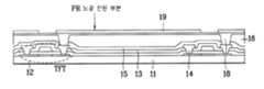
도 3a 내지 3e는 본 발명에 따른 유기 EL 소자의 제조 공정에 따른 평면도이고, 도 4a 내지 도 4e는 각각 도 3a 내지 도 3e 공정에서의 A-A 방향 단면도이다.3A to 3E are plan views according to the manufacturing process of the organic EL device according to the present invention, and FIGS. 4A to 4E are cross-sectional views along the A-A direction in the processes of FIGS. 3A to 3E, respectively.
본 발명에 따른 유기 EL 소자의 제조방법은 우선, 도 3a 및 도 4a에 도시된 바와 같이, 투명 기판(31)상에 픽셀 단위로 TFT(Thin Film Transistor)(32)를 형성한다.In the method of manufacturing the organic EL device according to the present invention, first, as shown in FIGS. 3A and 4A, a TFT (Thin Film Transistor) 32 is formed on a
즉, 투명 기판(31)상에 비정질 실리콘(amorphus silicon)을 형성하고, 비정 질 실리콘의 표면에 레이저를 조사함으로써 비정질 실리콘을 용융 재결정화하여 다결정 실리콘(poly Silicon)막을 형성한 다음에 포토 및 식각 공정으로 상기 다결정 실리콘막을 섬 형상으로 패터닝하여 반도체막(32a)을 형성하고, 반도체막(32a)을 포함한 전면에 게이트 절연막(32b)을 형성하고, 게이트 절연막(32b)상에 예를 들어 크롬(Cr)으로 이루어진 금속막을 형성한 후 포토 및 식각 공정으로 상기 금속막을 패터닝하여 게이트 절연막(32b)상의 반도체막(32a)의 중앙 부분에 대응하여 중첩되는 위치에 게이트 전극(32c)을 형성한다.That is, amorphous silicon is formed on the
그 다음, 상기 게이트 전극(32c)을 마스크로 상기 반도체막(32a)에 대하여 p형 또는 n형의 불순물을 주입하고, 주입된 불순물을 활성화시키기 위해서 가열 처리를 실시하여, 반도체막(32a)에 소오스 영역(32d) 및 드레인 영역(32e)을 형성한다.Subsequently, a p-type or n-type impurity is implanted into the
이렇게 해서, TFT(32)를 완성한다.In this way, the
이어, 상기 TFT(32)를 포함한 전면에 제 1 절연막(33)을 형성한 다음에 상기 제 1 절연막(33)과 게이트 절연막(32b)을 관통하여 TFT(32)의 소오스 전극(32d) 및 드레인 전극(32e)에 각각 연결되는 콘택(34)을 형성하고, 전면에 제 2 절연막(35)을 형성한다.Subsequently, after forming the first insulating
그 다음으로 도 3b 및 도 4b에 도시된 바와 같이, 제 2 절연막(35)상에 평탄화 절연막(36)을 형성하고, 상기 드레인 전극(32e)에 연결되는 콘택(34) 표면이 노출되도록 상기 평탄화 절연막(36)과 제 2 절연막(35)을 선택적으로 제거하여 비아홀(37)을 형성한다.3B and 4B, the
이어, 도 3c 및 도 4c에 도시된 바와 같이, 어노드 전극을 분리시킬 부분(픽셀의 경계 부분)에 격벽(38)을 형성한다.Subsequently, as shown in FIGS. 3C and 4C, the
이때, 상기 격벽(38)은 하부에서보다 상부에서 넓은 폭을 갖도록 오버행(Over-hang) 구조로 형성한다.In this case, the
예를 들어, 도 5a와 같이 역사다리꼴 모양으로 형성하거나, 도 5b 및 도 5c와 같이 처마 형태로 형성한다. 또한, 도 5d 및 도 5e와 같이 다층 레이어(layer)를 사용해도 되며, 그 재료로는 유기물, 무기물, 메탈 및 이들의 혼합물을 이용한다.For example, it may be formed in an inverted trapezoidal shape as shown in FIG. 5A or in an eave shape as shown in FIGS. 5B and 5C. In addition, a multilayer layer may be used as shown in FIGS. 5D and 5E, and organic materials, inorganic materials, metals, and mixtures thereof may be used as the material.
그 다음에 도 3d 및 4d에 도시된 바와 같이, 상기 바이홀(37)이 매립될 수 있도록 전면에 어노드 전극용 물질을 증착한다.3D and 4D, an anode electrode material is deposited on the front surface so that the bi-hole 37 can be buried.
상기 어노드 전극용 물질로는 반사율이 좋은 도전성 물질 특히, Cr, Cu, W, Au, Ni, Al, AlNd, Ag, Ti, Ta 등의 메탈이나, 이것들의 합금 또는 이들을 이용한 다층막을 사용한다.As the anode electrode material, a conductive material having good reflectance, in particular, metals such as Cr, Cu, W, Au, Ni, Al, AlNd, Ag, Ti, Ta, alloys thereof, or a multilayer film using them are used.
상기 격벽(38)이 어노드 전극을 분리시킬 부분에 형성되어 있으므로 어노드 전극용 물질 증착시에 자동적으로 어노드 전극이 분리되게 된다.Since the
즉, 상기 어노드 전극용 물질은 평탄화 절연막(36) 위에 뿐만 아니라 격벽(38)에도 형성되게 되는데, 격벽(38) 위의 어노드 전극용 물질과 평탄화 절연막(36) 위의 어노드 전극용 전극 물질은 자동적으로 분리되게 되며, 상기 평탄화 절연막(36) 위에는 어노드 전극(39)이 형성되게 되는 것이다.That is, the anode electrode material is formed not only on the
이어, 도 3e 및 도 4e에 도시된 바와 같이, 발광 영역을 제외한 나머지 부분에 절연막(40)을 형성한다.Next, as shown in FIGS. 3E and 4E, the insulating
상기 절연막(40)으로는 무기 절연체 또는 유기 절연체를 이용한다.An inorganic insulator or an organic insulator is used as the insulating
이때, 절연막(40)으로 무기 절연체를 이용하는 경우에는 예를 들어 SiNx, SiOx를 사용하는 것이 바람직하고, 유기 절연체를 사용하는 경우에는 예를 들어 폴리미드(polyimide), 폴리아크릴(polyacryl), novolac 계열의 물질을 사용하는 것이 바람직하다.In this case, when an inorganic insulator is used as the insulating
그리고, 도시하지 않았지만, 상기 절연막(40)을 포함한 전면에 유기 EL층을 형성하고 유기 EL층상에 캐소드 전극을 적층시켜 본 발명에 따른 유기 EL 소자를 완성한다.Although not shown, an organic EL layer is formed on the entire surface including the insulating
상기와 같은 본 발명의 유기 EL 소자의 제조방법은 다음과 같은 효과가 있다.The manufacturing method of the organic electroluminescent element of this invention as mentioned above has the following effects.
어노드 전극을 분리시킬 부분에 미리 격벽을 형성하여 어노드 전극용 물질 성막시에 자동적으로 어노드 전극이 분리되게 된다.The partition wall is formed in advance in the portion where the anode electrode is to be separated so that the anode electrode is automatically separated at the time of forming the material for the anode electrode.
따라서, 어노드 전극의 분리를 위해 포토 공정을 실시하지 않아도 되므로, 포토레지스트 제거 공정으로 인해 어노드 전극이 평탄화 절연막으로부터 박리되는 현상을 방지할 수 있다.Therefore, since the photo process does not have to be performed for separation of the anode electrode, it is possible to prevent the anode electrode from being peeled from the planarization insulating film due to the photoresist removing process.
또한, 어노드 전극이 박리되는 현상이 방지되므로 소자의 신뢰성을 향상시킬 수 있다.In addition, since the phenomenon in which the anode electrode is peeled off is prevented, the reliability of the device can be improved.
그리고, 복잡한 포토 공정(포토레지스트 도포 공정, 마스크 얼라인 공정, 노광 및 현상 공정, 어노드 전극 분리, 포토레지스트 제거 공정)을 실시하지 않아도 되므로 소자 제조 공정을 단순화시킬 수 있다.In addition, since a complicated photo process (photoresist coating process, mask alignment process, exposure and development process, anode electrode separation, and photoresist removal process) is not required, the device manufacturing process can be simplified.
이상 설명한 내용을 통해 당업자라면 본 발명의 기술 사상을 이탈하지 아니하는 범위에서 다양한 변경 및 수정이 가능함을 알 수 있을 것이다.Those skilled in the art will appreciate that various changes and modifications can be made without departing from the spirit of the present invention.
따라서, 본 발명의 기술적 범위는 실시예에 기재된 내용으로 한정하는 것이 아니라 특허 청구범위에 의해서 정해져야 한다.Therefore, the technical scope of the present invention should not be limited to the contents described in the examples, but should be defined by the claims.
Claims (8)
Translated fromKoreanPriority Applications (5)
| Application Number | Priority Date | Filing Date | Title |
|---|---|---|---|
| KR1020030090167AKR100587340B1 (en) | 2003-12-11 | 2003-12-11 | Manufacturing method of organic EL element |
| EP04029332AEP1542283B1 (en) | 2003-12-11 | 2004-12-10 | Organic electroluminescent device and its method of fabrication |
| US11/008,788US7579040B2 (en) | 2003-12-11 | 2004-12-10 | Method for fabricating organic electro-luminance device |
| JP2004358621AJP3981838B2 (en) | 2003-12-11 | 2004-12-10 | Manufacturing method of organic EL element |
| CNB2004100988084ACN100481485C (en) | 2003-12-11 | 2004-12-13 | Method for fabricating organic electro-luminance device |
Applications Claiming Priority (1)
| Application Number | Priority Date | Filing Date | Title |
|---|---|---|---|
| KR1020030090167AKR100587340B1 (en) | 2003-12-11 | 2003-12-11 | Manufacturing method of organic EL element |
Publications (2)
| Publication Number | Publication Date |
|---|---|
| KR20050057940A KR20050057940A (en) | 2005-06-16 |
| KR100587340B1true KR100587340B1 (en) | 2006-06-08 |
Family
ID=34511211
Family Applications (1)
| Application Number | Title | Priority Date | Filing Date |
|---|---|---|---|
| KR1020030090167AExpired - LifetimeKR100587340B1 (en) | 2003-12-11 | 2003-12-11 | Manufacturing method of organic EL element |
Country Status (5)
| Country | Link |
|---|---|
| US (1) | US7579040B2 (en) |
| EP (1) | EP1542283B1 (en) |
| JP (1) | JP3981838B2 (en) |
| KR (1) | KR100587340B1 (en) |
| CN (1) | CN100481485C (en) |
Families Citing this family (10)
| Publication number | Priority date | Publication date | Assignee | Title |
|---|---|---|---|---|
| US20070128401A1 (en)* | 2005-12-05 | 2007-06-07 | Wintek Corporation | Electrode separator |
| JP5019644B2 (en) | 2010-03-24 | 2012-09-05 | 株式会社ジャパンディスプレイセントラル | Organic EL device |
| US8922463B2 (en)* | 2010-04-26 | 2014-12-30 | Samsung Display Co., Ltd. | Organic light-emitting display apparatus |
| KR101351512B1 (en)* | 2010-10-25 | 2014-01-16 | 엘지디스플레이 주식회사 | Organic Light Emitting Diode and Method for fabricating the same |
| WO2015171849A2 (en) | 2014-05-07 | 2015-11-12 | Open Water Power, Incorporated | Hydrogen management in electrochemical systems |
| US9518866B2 (en) | 2014-08-22 | 2016-12-13 | Spectrasensors, Inc. | Spectrometer with variable beam power and shape |
| US9816860B2 (en) | 2014-08-22 | 2017-11-14 | Spectrasensors, Inc. | Spectrometer with active beam steering |
| US10024788B2 (en) | 2015-05-04 | 2018-07-17 | Spectrasensors, Inc. | Spectrometer with random beam profiles |
| CN105118929B (en)* | 2015-08-03 | 2018-01-02 | 京东方科技集团股份有限公司 | Electrode structure and organic light-emitting units and its manufacture method |
| CN118019391A (en) | 2021-08-11 | 2024-05-10 | 京东方科技集团股份有限公司 | Display substrate and electronic device |
Family Cites Families (8)
| Publication number | Priority date | Publication date | Assignee | Title |
|---|---|---|---|---|
| JP3813217B2 (en)* | 1995-03-13 | 2006-08-23 | パイオニア株式会社 | Method for manufacturing organic electroluminescence display panel |
| US5701055A (en)* | 1994-03-13 | 1997-12-23 | Pioneer Electronic Corporation | Organic electoluminescent display panel and method for manufacturing the same |
| JP3900769B2 (en) | 1999-01-26 | 2007-04-04 | 三菱化学株式会社 | Method for manufacturing organic electroluminescent device |
| JP4434411B2 (en)* | 2000-02-16 | 2010-03-17 | 出光興産株式会社 | Active drive type organic EL light emitting device and manufacturing method thereof |
| TW461228B (en)* | 2000-04-26 | 2001-10-21 | Ritdisplay Corp | Method to manufacture the non-photosensitive polyimide pixel definition layer of organic electro-luminescent display panel |
| JP2002083691A (en)* | 2000-09-06 | 2002-03-22 | Sharp Corp | Active matrix driven organic LED display device and method of manufacturing the same |
| US6664730B2 (en)* | 2001-07-09 | 2003-12-16 | Universal Display Corporation | Electrode structure of el device |
| JP2003109773A (en)* | 2001-07-27 | 2003-04-11 | Semiconductor Energy Lab Co Ltd | Light emitting device, semiconductor device, and manufacturing method thereof |
- 2003
- 2003-12-11KRKR1020030090167Apatent/KR100587340B1/ennot_activeExpired - Lifetime
- 2004
- 2004-12-10EPEP04029332Apatent/EP1542283B1/ennot_activeExpired - Lifetime
- 2004-12-10USUS11/008,788patent/US7579040B2/enactiveActive
- 2004-12-10JPJP2004358621Apatent/JP3981838B2/ennot_activeExpired - Lifetime
- 2004-12-13CNCNB2004100988084Apatent/CN100481485C/ennot_activeExpired - Lifetime
Also Published As
| Publication number | Publication date |
|---|---|
| JP3981838B2 (en) | 2007-09-26 |
| EP1542283A2 (en) | 2005-06-15 |
| JP2005174940A (en) | 2005-06-30 |
| US20050129840A1 (en) | 2005-06-16 |
| EP1542283A3 (en) | 2006-07-26 |
| EP1542283B1 (en) | 2011-06-15 |
| CN100481485C (en) | 2009-04-22 |
| US7579040B2 (en) | 2009-08-25 |
| CN1627872A (en) | 2005-06-15 |
| KR20050057940A (en) | 2005-06-16 |
Similar Documents
| Publication | Publication Date | Title |
|---|---|---|
| CN104733500B (en) | Organic light-emitting display device and its restorative procedure | |
| KR101107252B1 (en) | Thin film transistor substrate of electroluminescent display panel and manufacturing method thereof | |
| EP1724854B1 (en) | Organic electroluminescent device and method for manufacturing the same | |
| CN100485994C (en) | Organic electroluminescence device and manufacturing method thereof | |
| US7615923B2 (en) | Dual-plate organic electro-luminescent device and method for manufacturing the same | |
| KR20150075017A (en) | Organic light emitting display device, method for repair of the same and | |
| US20070012926A1 (en) | Display device with reduced number of wires and manufacturing method thereof | |
| JP2006146205A (en) | Flat panel display device and manufacturing method thereof | |
| JP4203369B2 (en) | Active matrix organic electroluminescent device and method for manufacturing the same | |
| KR100699995B1 (en) | Organic electroluminescent device and manufacturing method thereof | |
| KR100587340B1 (en) | Manufacturing method of organic EL element | |
| CN104681747B (en) | The method for manufacturing display device | |
| US8564194B2 (en) | Organic light emitting diode device and method for fabricating the same | |
| KR20090021442A (en) | Organic light emitting display device and manufacturing method | |
| KR100531292B1 (en) | method for fabricating of organic electroluminescence display panel | |
| US8860915B2 (en) | Display device | |
| KR100632525B1 (en) | Organic thin film transistor manufacturing method and transistor source / drain electrode forming method | |
| KR100685418B1 (en) | Organic EL device and method of manufacturing same | |
| KR20070056175A (en) | Organic light emitting display device and manufacturing method | |
| KR20050105855A (en) | Organic electro-luminescence display device and method for fabricating of the same | |
| KR20080060523A (en) | Organic light emitting diode display and manufacturing method thereof | |
| KR20060030438A (en) | Manufacturing method of organic EL element | |
| KR20090131397A (en) | OLED display device and manufacturing method | |
| KR20080002514A (en) | Dual plate organic electroluminescent device and manufacturing method thereof |
Legal Events
| Date | Code | Title | Description |
|---|---|---|---|
| A201 | Request for examination | ||
| PA0109 | Patent application | Patent event code:PA01091R01D Comment text:Patent Application Patent event date:20031211 | |
| PA0201 | Request for examination | ||
| PG1501 | Laying open of application | ||
| E902 | Notification of reason for refusal | ||
| PE0902 | Notice of grounds for rejection | Comment text:Notification of reason for refusal Patent event date:20051229 Patent event code:PE09021S01D | |
| E701 | Decision to grant or registration of patent right | ||
| PE0701 | Decision of registration | Patent event code:PE07011S01D Comment text:Decision to Grant Registration Patent event date:20060406 | |
| GRNT | Written decision to grant | ||
| PR0701 | Registration of establishment | Comment text:Registration of Establishment Patent event date:20060530 Patent event code:PR07011E01D | |
| PR1002 | Payment of registration fee | Payment date:20060601 End annual number:3 Start annual number:1 | |
| PG1601 | Publication of registration | ||
| PR1001 | Payment of annual fee | Payment date:20090323 Start annual number:4 End annual number:4 | |
| PR1001 | Payment of annual fee | Payment date:20100318 Start annual number:5 End annual number:5 | |
| PR1001 | Payment of annual fee | Payment date:20110329 Start annual number:6 End annual number:6 | |
| FPAY | Annual fee payment | ||
| PR1001 | Payment of annual fee | Payment date:20120330 Start annual number:7 End annual number:7 | |
| FPAY | Annual fee payment | ||
| PR1001 | Payment of annual fee | Payment date:20130329 Start annual number:8 End annual number:8 | |
| PR1001 | Payment of annual fee | Payment date:20140328 Start annual number:9 End annual number:9 | |
| FPAY | Annual fee payment | Payment date:20150429 Year of fee payment:10 | |
| PR1001 | Payment of annual fee | Payment date:20150429 Start annual number:10 End annual number:10 | |
| FPAY | Annual fee payment | Payment date:20160428 Year of fee payment:11 | |
| PR1001 | Payment of annual fee | Payment date:20160428 Start annual number:11 End annual number:11 | |
| FPAY | Annual fee payment | Payment date:20170413 Year of fee payment:12 | |
| PR1001 | Payment of annual fee | Payment date:20170413 Start annual number:12 End annual number:12 | |
| FPAY | Annual fee payment | Payment date:20180416 Year of fee payment:13 | |
| PR1001 | Payment of annual fee | Payment date:20180416 Start annual number:13 End annual number:13 | |
| FPAY | Annual fee payment | Payment date:20190417 Year of fee payment:14 | |
| PR1001 | Payment of annual fee | Payment date:20190417 Start annual number:14 End annual number:14 | |
| PR1001 | Payment of annual fee | Payment date:20200422 Start annual number:15 End annual number:15 | |
| PR1001 | Payment of annual fee | Payment date:20210415 Start annual number:16 End annual number:16 | |
| PR1001 | Payment of annual fee | Payment date:20220415 Start annual number:17 End annual number:17 | |
| PR1001 | Payment of annual fee | Payment date:20230417 Start annual number:18 End annual number:18 | |
| PC1801 | Expiration of term | Termination date:20240611 Termination category:Expiration of duration |