KR100587140B1 - Dual damascene pattern formation method of semiconductor device - Google Patents
Dual damascene pattern formation method of semiconductor deviceDownload PDFInfo
- Publication number
- KR100587140B1 KR100587140B1KR1020030047109AKR20030047109AKR100587140B1KR 100587140 B1KR100587140 B1KR 100587140B1KR 1020030047109 AKR1020030047109 AKR 1020030047109AKR 20030047109 AKR20030047109 AKR 20030047109AKR 100587140 B1KR100587140 B1KR 100587140B1
- Authority
- KR
- South Korea
- Prior art keywords
- forming
- etching
- gas
- etching process
- trench
- Prior art date
- Legal status (The legal status is an assumption and is not a legal conclusion. Google has not performed a legal analysis and makes no representation as to the accuracy of the status listed.)
- Expired - Fee Related
Links
Images


Classifications
- H—ELECTRICITY
- H01—ELECTRIC ELEMENTS
- H01L—SEMICONDUCTOR DEVICES NOT COVERED BY CLASS H10
- H01L21/00—Processes or apparatus adapted for the manufacture or treatment of semiconductor or solid state devices or of parts thereof
- H01L21/70—Manufacture or treatment of devices consisting of a plurality of solid state components formed in or on a common substrate or of parts thereof; Manufacture of integrated circuit devices or of parts thereof
- H01L21/71—Manufacture of specific parts of devices defined in group H01L21/70
- H01L21/768—Applying interconnections to be used for carrying current between separate components within a device comprising conductors and dielectrics
- H01L21/76801—Applying interconnections to be used for carrying current between separate components within a device comprising conductors and dielectrics characterised by the formation and the after-treatment of the dielectrics, e.g. smoothing
- H01L21/76802—Applying interconnections to be used for carrying current between separate components within a device comprising conductors and dielectrics characterised by the formation and the after-treatment of the dielectrics, e.g. smoothing by forming openings in dielectrics
- H01L21/76807—Applying interconnections to be used for carrying current between separate components within a device comprising conductors and dielectrics characterised by the formation and the after-treatment of the dielectrics, e.g. smoothing by forming openings in dielectrics for dual damascene structures
- H—ELECTRICITY
- H01—ELECTRIC ELEMENTS
- H01L—SEMICONDUCTOR DEVICES NOT COVERED BY CLASS H10
- H01L21/00—Processes or apparatus adapted for the manufacture or treatment of semiconductor or solid state devices or of parts thereof
- H01L21/02—Manufacture or treatment of semiconductor devices or of parts thereof
- H01L21/027—Making masks on semiconductor bodies for further photolithographic processing not provided for in group H01L21/18 or H01L21/34
- H01L21/0271—Making masks on semiconductor bodies for further photolithographic processing not provided for in group H01L21/18 or H01L21/34 comprising organic layers
- H01L21/0273—Making masks on semiconductor bodies for further photolithographic processing not provided for in group H01L21/18 or H01L21/34 comprising organic layers characterised by the treatment of photoresist layers
- H01L21/0274—Photolithographic processes
- H01L21/0276—Photolithographic processes using an anti-reflective coating
- H—ELECTRICITY
- H01—ELECTRIC ELEMENTS
- H01L—SEMICONDUCTOR DEVICES NOT COVERED BY CLASS H10
- H01L21/00—Processes or apparatus adapted for the manufacture or treatment of semiconductor or solid state devices or of parts thereof
- H01L21/02—Manufacture or treatment of semiconductor devices or of parts thereof
- H01L21/04—Manufacture or treatment of semiconductor devices or of parts thereof the devices having potential barriers, e.g. a PN junction, depletion layer or carrier concentration layer
- H01L21/18—Manufacture or treatment of semiconductor devices or of parts thereof the devices having potential barriers, e.g. a PN junction, depletion layer or carrier concentration layer the devices having semiconductor bodies comprising elements of Group IV of the Periodic Table or AIIIBV compounds with or without impurities, e.g. doping materials
- H01L21/30—Treatment of semiconductor bodies using processes or apparatus not provided for in groups H01L21/20 - H01L21/26
- H01L21/31—Treatment of semiconductor bodies using processes or apparatus not provided for in groups H01L21/20 - H01L21/26 to form insulating layers thereon, e.g. for masking or by using photolithographic techniques; After treatment of these layers; Selection of materials for these layers
- H01L21/3105—After-treatment
- H01L21/311—Etching the insulating layers by chemical or physical means
- H01L21/31105—Etching inorganic layers
- H01L21/31111—Etching inorganic layers by chemical means
- H01L21/31116—Etching inorganic layers by chemical means by dry-etching
- H—ELECTRICITY
- H01—ELECTRIC ELEMENTS
- H01L—SEMICONDUCTOR DEVICES NOT COVERED BY CLASS H10
- H01L21/00—Processes or apparatus adapted for the manufacture or treatment of semiconductor or solid state devices or of parts thereof
- H01L21/02—Manufacture or treatment of semiconductor devices or of parts thereof
- H01L21/04—Manufacture or treatment of semiconductor devices or of parts thereof the devices having potential barriers, e.g. a PN junction, depletion layer or carrier concentration layer
- H01L21/18—Manufacture or treatment of semiconductor devices or of parts thereof the devices having potential barriers, e.g. a PN junction, depletion layer or carrier concentration layer the devices having semiconductor bodies comprising elements of Group IV of the Periodic Table or AIIIBV compounds with or without impurities, e.g. doping materials
- H01L21/30—Treatment of semiconductor bodies using processes or apparatus not provided for in groups H01L21/20 - H01L21/26
- H01L21/31—Treatment of semiconductor bodies using processes or apparatus not provided for in groups H01L21/20 - H01L21/26 to form insulating layers thereon, e.g. for masking or by using photolithographic techniques; After treatment of these layers; Selection of materials for these layers
- H01L21/3105—After-treatment
- H01L21/311—Etching the insulating layers by chemical or physical means
- H01L21/31127—Etching organic layers
- H01L21/31133—Etching organic layers by chemical means
- H01L21/31138—Etching organic layers by chemical means by dry-etching
- H—ELECTRICITY
- H01—ELECTRIC ELEMENTS
- H01L—SEMICONDUCTOR DEVICES NOT COVERED BY CLASS H10
- H01L21/00—Processes or apparatus adapted for the manufacture or treatment of semiconductor or solid state devices or of parts thereof
- H01L21/02—Manufacture or treatment of semiconductor devices or of parts thereof
- H01L21/04—Manufacture or treatment of semiconductor devices or of parts thereof the devices having potential barriers, e.g. a PN junction, depletion layer or carrier concentration layer
- H01L21/18—Manufacture or treatment of semiconductor devices or of parts thereof the devices having potential barriers, e.g. a PN junction, depletion layer or carrier concentration layer the devices having semiconductor bodies comprising elements of Group IV of the Periodic Table or AIIIBV compounds with or without impurities, e.g. doping materials
- H01L21/30—Treatment of semiconductor bodies using processes or apparatus not provided for in groups H01L21/20 - H01L21/26
- H01L21/31—Treatment of semiconductor bodies using processes or apparatus not provided for in groups H01L21/20 - H01L21/26 to form insulating layers thereon, e.g. for masking or by using photolithographic techniques; After treatment of these layers; Selection of materials for these layers
- H01L21/3105—After-treatment
- H01L21/311—Etching the insulating layers by chemical or physical means
- H01L21/31144—Etching the insulating layers by chemical or physical means using masks
Landscapes
- Engineering & Computer Science (AREA)
- Microelectronics & Electronic Packaging (AREA)
- Condensed Matter Physics & Semiconductors (AREA)
- General Physics & Mathematics (AREA)
- Manufacturing & Machinery (AREA)
- Computer Hardware Design (AREA)
- Physics & Mathematics (AREA)
- Power Engineering (AREA)
- Chemical & Material Sciences (AREA)
- Chemical Kinetics & Catalysis (AREA)
- General Chemical & Material Sciences (AREA)
- Inorganic Chemistry (AREA)
- Internal Circuitry In Semiconductor Integrated Circuit Devices (AREA)
Abstract
Translated fromKoreanDescription
Translated fromKorean도 1 내지 도 8은 본 발명의 바람직한 실시예에 따른 반도체 소자의 듀얼 다마신 패턴 형성방법을 설명하기 위하여 도시한 단면도들이다.1 to 8 are cross-sectional views illustrating a method for forming a dual damascene pattern of a semiconductor device according to an exemplary embodiment of the present invention.
도 9는 종래기술에 따른 듀얼 다마신 패턴 형성공정에 의해 패싯(facet) 현상이 발생된 TEM(Transmission Electon Microscope) 사진이다.9 is a transmission electron microscope (TEM) photograph in which a facet phenomenon is generated by a dual damascene pattern forming process according to the related art.
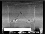
도 10a 내지 도 10c는 종래기술에 따른 듀얼 다마신 패턴 형성공정에 의해 발생된 측벽 펜스(sidewall fence)를 도시한 SEM(Scanning Electon Microscope) 사진들이다.10A to 10C are scanning electron microscope (SEM) photographs showing sidewall fences generated by a dual damascene pattern forming process according to the prior art.
〈도면의 주요 부분에 대한 부호의 설명〉<Explanation of symbols for main parts of drawing>
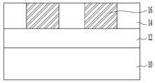
10 : 반도체 기판 12 : 반도체 구조물층10
14 : 제1 층간절연막 16 : 하부 금속배선14: first interlayer insulating film 16: lower metal wiring
18 : 확산방지막 20 : 제2 층간절연막18
22 : 캡핑층 24 : 비아홀22: capping layer 24: via hole
26 : 유기 BARC 28 : 포토레지스트 패턴26: organic BARC 28: photoresist pattern
30 : 트렌치30: trench
본 발명은 반도체 소자의 듀얼 다마신 패턴 형성방법에 관한 것으로, 특히 선(先)비아방식의 듀얼 다마신 공정에서 발생되는 측벽 펜스를 제어하여 금속배선의 신뢰성을 향상시킬 수 있는 반도체 소자의 듀얼 다마신 패턴 형성방법에 관한 것이다.The present invention relates to a method for forming a dual damascene pattern of a semiconductor device, and in particular, to control the sidewall fence generated in a pre-via dual damascene process to improve the reliability of metal wiring. It relates to a method of forming a drank pattern.
반도체 소자 또는 전자 소자 등에 있어서는, 금속배선 형성기술로서 절연막 상에 알루미늄(Al) 또는 텅스텐(W) 등과 같은 도전체막이 증착된 후, 상기 도전체막이 통상의 포토리소그래피(photolithography) 공정 및 건식식각(dry etching) 공정을 통해 패터닝됨으로써 금속배선이 형성되는 기술이 확립되어 이 분야에서 널리 이용되고 있다. 특히, 최근에는 반도체 소자 중에서 고집적화와 고성능화가 요구되는 로직(logic) 소자를 중심으로 해서 RC 지연을 줄이기 위한 일환으로 알루미늄 또는 텅스텐 대신에 구리(Cu)와 같이 비저항이 낮은 금속을 배선으로 이용하는 방법이 연구되고 있다. 상기 RC에서, 'R'은 배선 저항을 나타내고, 'C'는 절연막의 유전율을 나타낸다.In a semiconductor device or an electronic device, a conductor film such as aluminum (Al) or tungsten (W) is deposited on an insulating film as a metal wiring forming technique, and then the conductor film is subjected to a conventional photolithography process and dry etching ( The technique of forming metal wiring by patterning through dry etching process has been established and widely used in this field. In particular, recently, a method of using a low-resistance metal such as copper (Cu) instead of aluminum or tungsten as wiring to reduce the RC delay centering on logic devices requiring high integration and high performance among semiconductor devices has recently been used. Is being studied. In RC, 'R' represents wiring resistance, and 'C' represents dielectric constant of the insulating film.
구리를 이용한 금속배선 형성공정에서는 알루미늄 또는 텅스텐에 비해 패터닝 공정이 어렵다. 이에 따라, 먼저 트렌치(trench)를 형성한 후 상기 트렌치가 매 립되도록 금속배선을 형성하는 소위 '다마신(damascene)' 공정이 사용되고 있다. 현재 일반적으로 사용되는 공정으로는 싱글 다마신 공정(single damascene)과 듀얼 다마신 공정(Dual damascene)이 있다. 싱글 다마신 공정은 비아홀(via hole)을 형성한 후 도전재료로 상기 비아홀을 매립하고 그 상부에 배선용 트렌치를 형성한 후 다시 배선재료로 상기 트렌치를 매립하여 금속배선을 형성하는 방법이다. 듀얼 다마신 공정은 비아홀과 배선용 트렌치를 형성한 후 배선재료를 동시에 비아홀과 배선용 트렌치를 매립하여 금속배선을 형성하는 방법이다. 이러한 다마신 공정을 기본으로 하여 다양한 금속배선 형성방법들이 제시되고 있다.In the metallization process using copper, the patterning process is more difficult than aluminum or tungsten. Accordingly, a so-called 'damascene' process is used in which a trench is first formed and a metal wiring is formed to fill the trench. Currently commonly used processes include the single damascene process and the dual damascene process. The single damascene process is a method of forming a via hole and then filling the via hole with a conductive material, forming a wiring trench on the upper portion thereof, and then filling the trench with a wiring material to form a metal wiring. The dual damascene process is a method for forming metal vias by forming via holes and wiring trenches and then filling the wiring material with via holes and wiring trenches at the same time. Based on the damascene process, various metal wire forming methods have been proposed.
그러나, 상기에서 설명한 다마신 공정을 이용한 금속배선 형성공정들에서는 노광장비의 적층능력(overlay)의 한계상 많은 문제점들이 발생되고 있다. 특히 0.13㎛ 이하의 고성능 반도체 소자의 금속배선 형성공정에서 적층능력의 한계가 발생되고 있다. 예컨대, 트렌치를 형성하기 위한 식각공정후 비아 마스크 패터닝(via mask patterning)시 트렌치의 모서리(edge) 부분에서 난반사 등으로 인하여 비아 마스크의 형성이 매우 어려워지는 등 무수히 많은 문제점을 야기시킬 수 있다. 또한, 층간절연막으로 유전상수가 낮은 막을 사용하면서 식각정지층(etch stopping layer) 등의 사용제약에 의해 도 9와 같이 페싯(facet; 원형안) 현상 등이 발생된다.However, in the metal wiring forming processes using the damascene process described above, many problems arise due to the limitation of the overlay capability of the exposure apparatus. In particular, there is a limit in lamination capability in the metallization formation process of a high-performance semiconductor device of 0.13 μm or less. For example, in the case of via mask patterning after the etching process for forming the trench, a large number of problems may occur, such as the formation of the via mask becomes very difficult due to the diffuse reflection at the edge of the trench. In addition, a facet phenomenon is generated as shown in FIG. 9 due to the use of a film having a low dielectric constant as the interlayer insulating film, and the use of an etch stopping layer.
이러한 문제점들을 극복하기 위하여 선(先)비아방식을 사용하고 있다, 하지만, 도 10a 내지 도 10c에서 도시된 측벽 펜스(sidewall fence; 'A'참조)와 같이, 트렌치를 형성하기 위한 건식식각후 비아홀에 채워져 있는 유기(organic) BARC(Bottom AntiReflection Coating) 으로 인해 스페이서(spacer)가 형성된 것처럼 표족하게 남게 된다. 여기서, 도 10a는 트렌치를 완전식각하는 경우 발생되는 측벽 펜스를 도시한 SEM 사진이다. 도 10b는 트렌치를 부분식각하는 경우 발생되는 측벽 펜스를 도시한 SEM 사진이다. 도 10c는 도 10a 또는 도 10b에서 트렌치가 형성된 후 트렌치 형성용 식각 마스크인 포토레지스트 패턴(photoresist pattern)을 제거한 후 발생되는 측벽 펜스를 도시한 SEM 사진이다.In order to overcome these problems, a pre-via method is used. However, as in the sidewall fence (see 'A') shown in FIGS. 10A to 10C, a via hole after dry etching to form a trench is shown. The organic BARC (Bottom AntiReflection Coating) filled on the surface leaves the spacer as if formed. Here, FIG. 10A is a SEM photograph showing the sidewall fence generated when the trench is completely etched. FIG. 10B is a SEM photograph illustrating a sidewall fence generated when the trench is partially etched. FIG. FIG. 10C is a SEM photograph illustrating sidewall fences generated after removing the photoresist pattern, which is an etching mask for forming trenches, after the trench is formed in FIG. 10A or 10B.
상기에서 측벽 펜스는 후속 공정인 고주파 스퍼터(RF sputter) 등의 공정후에도 잘 제거가 되지 않아 금속배선 형성시 베리어막(barrier film)/시드층(seed layer) 형성공정 및 구리 전기도금공정에 불안정성 요인으로 작용하여 구리배선의 신뢰성을 저하시킨다. 측벽 펜스(A)는 O2 가스 등이 첨가된 혼합가스를 이용한 식각공정을 통해 제거가 가능하다. 그렇지만, O2 가스 등이 첨가된 혼합가스를 이용하여 식각공정을 진행하는 경우에는 트렌치 형성용 마스크인 포토레지스트 패턴(photoresist pattern)의 측벽 또한 손실되게 된다. 이러한 포토레지스트 패턴의 측벽 손실은 결국 트렌치의 상부의 손상(damage)를 야기시키고, 심한 경우에는 인접한 트렌치의 상부와의 브릿지(bridge)를 유발시킨다.The sidewall fence is not removed well after the process such as RF sputter, which is a subsequent process, and thus causes instability in the barrier film / seed layer forming process and the copper electroplating process when forming the metal wiring. This reduces the reliability of the copper wiring. The side wall fence A may be removed through an etching process using a mixed gas including O2 gas or the like. However, when the etching process is performed using a mixed gas containing O2 gas or the like, sidewalls of a photoresist pattern, which is a trench forming mask, are also lost. Sidewall loss of such photoresist patterns eventually leads to damage of the tops of the trenches and, in severe cases, to bridges with the tops of adjacent trenches.
따라서, 본 발명의 바람직한 실시예는 선비아방식의 듀얼 다마신 공정에서 발생되는 측벽 펜스를 제어하여 금속배선의 신뢰성을 향상시키는데 그 목적이 있 다.
Accordingly, a preferred embodiment of the present invention is to control the sidewall fence generated in the sun via dual damascene process to improve the reliability of the metal wiring.
본 발명의 일측면에 따르면, 하지층이 형성된 반도체 기판 상에 층간절연막이 형성되는 단계와, 상기 층간절연막 상에 캡핑층이 형성되는 단계와, 비아홀 형성형 식각 마스크를 이용한 식각공정을 통해 상기 캡핑층 및 상기 층간절연막이 패터닝되어 비아홀이 형성되는 단계와, 상기 비아홀이 매립되도록 전체 구조 상부에 유기 BARC가 증착되는 단계와, 인접한 상기 비아홀 사이에 형성된 상기 층간절연막이 노출되도록 트렌치 형성용 식각 마스크를 이용한 식각공정을 통해 상기 유기 BARC 및 상기 캡핑층이 식각되는 단계와, 상기 트렌치 형성용 식각 마스크를 이용하여 적어도 2회 식각공정을 실시하여 상기 유기 BARC와, 상기 비아홀 사이에 형성된 상기 층간절연막이 리세스(recess)되는 단계와, 상기 단계에서 잔류되는 상기 유기 BARC를 제거하여 트렌치가 형성되는 단계를 포함하는 반도체 소자의 듀얼 다마신 패턴 형성방법이 제공된다.According to an aspect of the present invention, the cap is formed by forming an interlayer insulating film on a semiconductor substrate on which an underlayer is formed, forming a capping layer on the interlayer insulating film, and an etching process using a via hole forming etching mask. Forming a via hole by patterning the ping layer and the interlayer insulating layer, depositing an organic BARC on the entire structure to fill the via hole, and etching the trench forming mask to expose the interlayer insulating layer formed between the adjacent via holes. Etching the organic BARC and the capping layer through an etching process, and performing an etching process at least twice using an etching mask for forming the trench to remove the interlayer insulating layer formed between the organic BARC and the via hole. A trench that is recessed and the organic BARC remaining in the step is removed The dual damascene patterning method of a semiconductor device including a step to be formed is provided.
이하, 첨부된 도면을 참조하여 본 발명의 바람직한 실시예를 설명하기로 한다. 그러나, 본 발명은 이하에서 개시되는 실시예에 한정되는 것이 아니라 서로 다른 다양한 형태로 구현될 수 있으며, 단지 본 실시예는 본 발명의 개시가 완전하도록하며 통상의 지식을 가진자에게 발명의 범주를 완전하게 알려주기 위해 제공되는 것이다.Hereinafter, with reference to the accompanying drawings will be described a preferred embodiment of the present invention. However, the present invention is not limited to the embodiments disclosed below, but may be implemented in various forms, and only the present embodiments are intended to complete the disclosure of the present invention and to those skilled in the art. It is provided for complete information.
도 1 내지 도 8은 본 발명의 바람직한 실시예에 따른 반도체 소자의 듀얼 다 마신 패턴 형성방법을 설명하기 위하여 도시한 단면도들이다. 여기서, 도 1 내지 도 8에 도시된 참조부호들 중 서로 동일한 참조부호는 동일한 기능을 하는 동일한 구성요소이다.1 to 8 are cross-sectional views illustrating a method of forming a dual damascene pattern of a semiconductor device according to an exemplary embodiment of the present invention. Here, the same reference numerals among the reference numerals shown in FIGS. 1 to 8 are the same components having the same function.
도 1을 참조하면, 소정의 반도체 구조물층(12)이 형성된 반도체 기판(10)이 제공된다. 여기서, 상기 반도체 구조물층(12)은 트랜지스터, 메모리 셀, 캐패시터, 접합층 및 도전층 등이 포함될 수 있다. 이후, 상기 반도체 구조물층(12) 상에는 저유전 물질로, 예컨대, PETEOS(Plasma Enhanced Tetra Ethyle Ortho Silicate), USG(Un-doped Silicate Glass), FSG(Fluorinated Silicate Glass), 실리콘 산화물, 불소 함유 실리콘 산화물 또는 불소 함유 산화물 등을 이용하여 절연막(이하, '제1 층간절연막'이라 함)(14)이 증착된다. 일반적으로, 불소 함유 실리콘 산화물은 실리콘 산화물보다 낮은 유전율을 가지며, 이러한 유전율은 불소 함유량을 조절하여 그 제어가 가능하다.Referring to FIG. 1, a
이후, 리소그래피 공정을 실시하여 상기 제1 층간절연막(14)에 콘택홀(미도시)이 형성되고, 상기 콘택홀이 매립되도록 하부 금속배선(16)이 순차적으로 형성된다. 이때, 하부 금속배선(16)은 구리, 텅스텐, Al, Pt(Platinum), Pd(Palladium), Ru(Rubidium), St(Strontium), Rh(Rhadium) 및 Co 중 어느 하나이다. 한편, 하부 금속배선(16)이 증착되기전 상기 콘택홀의 내부면에는 베리어막이 형성될 수 있으며, 이때, 상기 베리어막은 Ta, TaN, TaAlN, TaSiN, TaSi2, Ti, TiN, TiSiN, WN, Co 및 CoSi2중 어느 하나로 형성될 수 있다.Subsequently, a lithography process is performed to form contact holes (not shown) in the first
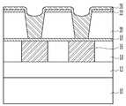
도 2를 참조하면, 도 1에서 하부 금속배선(16)이 형성된 후 전체 구조 상부에는 확산방지막(18)이 형성된다. 이때, 확산방지막(18)은 300Å 내지 1000Å의 두께로 형성된다. 이후, 상기 확산방지막(18) 상에는 제2 층간절연막(20)이 형성된다. 상기 제2 층간절연막(20)은 PETEOS, USG, FSG, 또는 SiO 또는 SiO2에 국부적으로 불소, 수소, 붕소 또는 인 등이 결합(substitutional) 또는 삽입(interstitial)된 막으로 형성될 수 있다. 이후, 상기 제1 층간절연막(20)은 CMP 공정을 통해 평탄화될 수 있다. 이후, 상기 제1 층간절연막(20) 상에는 캡핑층(capping layer; 22)이 형성된다. 이때, 상기 캡핑층(22)은 질화막(예컨대, 실리콘 질화막), 질산화막(예컨대, 실리콘 질산화막) 또는 SiC 등과 같이 탄소가 함유된 탄화막을 적어도 단층 또는 이 들이 복합구조로 이루어질 수 있다. 이때, 상기 캡핑층(22)은 50Å 내지 1000Å로 형성된다. 여기서, 상기 캡핑층(22)이 실리콘 질화막(SiN) 또는 실리콘 질산화막(SiON)으로 형성될 경우 반사방지 효과를 부수적으로 얻어 후속 공정을 통해 형성된 유기 BARC(26; 도 4참조)의 두께를 감소시킬 수 있다.Referring to FIG. 2, after the
도 3을 참조하면, 도 2에서 캡핑층(22)이 형성된 후, 선비아 방식으로 듀얼 다마신 공정이 실시된다. 우선, 전체 구조 상부에는 포토레지스트(photoresist)가 전면 코팅된 후, 포토 마스크(photomask)를 이용한 노광공정 및 현상공정을 순차적으로 실시하여 캡핑층(22)의 일부가 노출되는 비아홀 형성용 식각 마스크로 포토레지스트 패턴(photoresist pattern; 미도시)이 형성된다. 그런 다음, 상기 포토레지스트 패턴을 식각 마스크로 이용한 식각공정을 건식식각방식으로 실시하여 노출되 는 캡핑층(22)과 제2 층간절연막(20)을 순차적으로 식각하여 비아홀(24)이 형성된다. 상기 식각공정은 CxHyFz(x,y,z는 0 또는 자연수)가스를 주(main) 식각가스로 사용하고, O2, N2, Ar 또는 He 등의 불활성 기체원자 또는 분자를 첨가가스로 사용하여 실시된다. 이 경우, 주 식각가스인 CxHyFz에서 'x'의 비율을 증가시키거나, 첨가가스의 비율을 감소시키면 캡핑층(22), 예컨대, SiC에 대한 선택비가 증가된다. 또한, 첨가가스의 비율을 증가 또는 주 식각가스인 CxHyFz에서 'y', 'z'의 비율을 증가시키면 캡핑층(22), 예컨대, SiC에 대한 선택비를 낮출 수 있으며, SiC 건식식각시 제2 층간절연막(20), 예컨대, SiOC에 대한 선택비가 선택비를 증가시킬 수 있게 된다.Referring to FIG. 3, after the
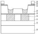
도 4 및 도 5를 참조하면, 도 3에서 비아홀(24)이 형성된 후 상기 비아홀(24)이 매립되도록 전체 구조 상부에는 유기 BARC(26)가 증착된다. 그런 다음, 전체 구조 상부에는 포토레지스트가 전면 코팅된 후, 포토 마스크를 이용한 노광공정 및 현상공정을 순차적으로 실시하여 트렌치 형성용 포토레지스트 패턴(28)이 형성된다. 그런 다음, 상기 포토레지스트 패턴(28)을 식각 마스크로 이용한 식각공정을 건식식각방식으로 실시하여 노출되는 유기 BARC(26)가 식각된다. 이때, 상기 식각공정은 O2, N2 또는 He 등을 주 식각가스로 사용한다. 그런 다음, 트렌치(30; 도 8참조)를 형성하기 위한 1차 식각공정으로, CxHyFz(x,y,z는 0 또는 자연수)가스를 주 식각가스로 사용하고, O2, N2, Ar 또는 He 등의 불활성 기체원자 또는 분자를 첨가가스로 사용하여 실시된다. 이때, 1차 식각공정은 목표치 트렌치(30) 깊이의 10% 내지 90%가 되도록 실시되는 것이 바람직하다. 이로써, 유기 BARC(26)이 리세스(recess)된다. 이러한 과정을 통해, 도 5와 같은 프로파일(profile)이 얻어진다.4 and 5, after the via
도 6을 참조하면, 도 5에서 1차 식각공정이 완료된 후, 측벽 펜스의 형성을 방지하기 위하여 식각공정을 통해 유기 BARC(26)이 부분 리세스된다. 이때, 상기 식각공정은 O2, N2 또는 He 등을 주 식각가스로 사용한다. 이에 따라, 상기 포토레지스트 패턴(28)의 상부 및 측벽도 부분 식각된다. 이러한 과정을 통해, 도 6과 같은 프로파일이 얻어진다.Referring to FIG. 6, after the primary etching process is completed in FIG. 5, the organic BARC 26 is partially recessed through the etching process to prevent the formation of the sidewall fence. In this case, the etching process uses O2 , N2 or He as the main etching gas. Accordingly, the top and sidewalls of the photoresist pattern 28 are also partially etched. Through this process, a profile as shown in FIG. 6 is obtained.
도 7을 참조하면, 이후, 2차 식각공정이 실시된다. 상기 2차 식각공정은 CxHyFz(x,y,z는 0 또는 자연수)가스를 주 식각가스로 사용하고, O2, N2, Ar 또는 He 등의 불활성 기체원자 또는 분자를 첨가가스로 사용하여 실시된다. 이러한 과정을 통해, 도 7과 같은 프로파일이 얻어진다.Referring to FIG. 7, a second etching process is then performed. In the secondary etching process, Cx Hy Fz (x, y, z is 0 or natural water) gas is used as the main etching gas, and an inert gas atom or molecule such as O2 , N2 , Ar or He is added. It is carried out using gas. Through this process, a profile as shown in FIG. 7 is obtained.
도 8을 참조하면, 도 7에서 2차 식각공정이 완료된 후, 식각공정을 통해 비아홀(24) 내에 잔류되는 유기 BARC(26)와, 잔류되는 유기 BARC(26)의 하부에 형성된 확산방지막(18)이 제거된다. 이때, 상기 캡핑층(22)이 부분 또는 완전히 제거된다. 이로써, 후속 공정을 통해 형성되는 상부 금속배선(미도시)과 하부 금속배선(16)이 접속된다.Referring to FIG. 8, after the secondary etching process is completed in FIG. 7, the organic BARC 26 remaining in the via
상기에서 설명한 본 발명의 기술적 사상은 바람직한 실시예에서 구체적으로 기술되었으나, 상기한 실시예는 그 설명을 위한 것이며 그 제한을 위한 것이 아님을 주의하여야 한다. 또한, 본 발명은 본 발명의 기술 분야의 통상의 전문가라면 본 발명의 기술적 사상의 범위 내에서 다양한 실시예가 가능함을 이해할 수 있을 것이다.Although the technical spirit of the present invention described above has been described in detail in a preferred embodiment, it should be noted that the above-described embodiment is for the purpose of description and not of limitation. In addition, the present invention will be understood by those skilled in the art that various embodiments are possible within the scope of the technical idea of the present invention.
상술한 바와 같이, 본 발명에 의하면, 듀얼 다마신 패턴 형성공정시 선비아 방식에서 발생되는 측벽 펜스(sidewall fence)의 발생을 억제하여 금속배선의 신뢰성을 향상시킬 수 있다.As described above, according to the present invention, it is possible to suppress the occurrence of sidewall fences generated in the sun via method during the dual damascene pattern forming process, thereby improving the reliability of the metal wiring.
Claims (7)
Translated fromKoreanPriority Applications (1)
| Application Number | Priority Date | Filing Date | Title |
|---|---|---|---|
| KR1020030047109AKR100587140B1 (en) | 2003-07-11 | 2003-07-11 | Dual damascene pattern formation method of semiconductor device |
Applications Claiming Priority (1)
| Application Number | Priority Date | Filing Date | Title |
|---|---|---|---|
| KR1020030047109AKR100587140B1 (en) | 2003-07-11 | 2003-07-11 | Dual damascene pattern formation method of semiconductor device |
Publications (2)
| Publication Number | Publication Date |
|---|---|
| KR20050007631A KR20050007631A (en) | 2005-01-21 |
| KR100587140B1true KR100587140B1 (en) | 2006-06-07 |
Family
ID=37220979
Family Applications (1)
| Application Number | Title | Priority Date | Filing Date |
|---|---|---|---|
| KR1020030047109AExpired - Fee RelatedKR100587140B1 (en) | 2003-07-11 | 2003-07-11 | Dual damascene pattern formation method of semiconductor device |
Country Status (1)
| Country | Link |
|---|---|
| KR (1) | KR100587140B1 (en) |
- 2003
- 2003-07-11KRKR1020030047109Apatent/KR100587140B1/ennot_activeExpired - Fee Related
Also Published As
| Publication number | Publication date |
|---|---|
| KR20050007631A (en) | 2005-01-21 |
Similar Documents
| Publication | Publication Date | Title |
|---|---|---|
| US7157366B2 (en) | Method of forming metal interconnection layer of semiconductor device | |
| US6861347B2 (en) | Method for forming metal wiring layer of semiconductor device | |
| CN100576494C (en) | Method for forming dual damascene wiring of semiconductor device using protective via capping layer | |
| US7470616B1 (en) | Damascene wiring fabrication methods incorporating dielectric cap etch process with hard mask retention | |
| US6372635B1 (en) | Method for making a slot via filled dual damascene low k interconnect structure without middle stop layer | |
| US6372631B1 (en) | Method of making a via filled dual damascene structure without middle stop layer | |
| US7217663B2 (en) | Via hole and trench structures and fabrication methods thereof and dual damascene structures and fabrication methods thereof | |
| US6383919B1 (en) | Method of making a dual damascene structure without middle stop layer | |
| US7176123B2 (en) | Method for manufacturing metal line of semiconductor device | |
| JP5047504B2 (en) | Method for manufacturing dual damascene wiring of semiconductor device using via capping protective film | |
| US20090163020A1 (en) | Method for Manufacturing Semiconductor Device | |
| KR100539444B1 (en) | Method for forming a metal line in semiconductor device | |
| KR100587140B1 (en) | Dual damascene pattern formation method of semiconductor device | |
| JP2008503073A (en) | Manufacturing method of layer structure | |
| KR100539443B1 (en) | Method for forming a metal line in semiconductor device | |
| US7112537B2 (en) | Method of fabricating interconnection structure of semiconductor device | |
| KR101103550B1 (en) | Metal wiring formation method of semiconductor device | |
| KR101138082B1 (en) | A method for forming a dual damascene pattern in semiconductor device | |
| KR100691105B1 (en) | Copper wiring formation method using dual damascene process | |
| KR101005737B1 (en) | Metal wiring formation method of semiconductor device | |
| KR101021176B1 (en) | Metal wiring formation method of semiconductor device | |
| KR101005738B1 (en) | Dual damascene pattern formation method of semiconductor device | |
| KR100539446B1 (en) | Method for forming a dual damascene pattern in semiconductor device | |
| KR100955838B1 (en) | Semiconductor device and wiring manufacturing method | |
| KR100447322B1 (en) | Method of forming a metal line in semiconductor device |
Legal Events
| Date | Code | Title | Description |
|---|---|---|---|
| PA0109 | Patent application | St.27 status event code:A-0-1-A10-A12-nap-PA0109 | |
| A201 | Request for examination | ||
| PA0201 | Request for examination | St.27 status event code:A-1-2-D10-D11-exm-PA0201 | |
| N231 | Notification of change of applicant | ||
| PN2301 | Change of applicant | St.27 status event code:A-3-3-R10-R13-asn-PN2301 St.27 status event code:A-3-3-R10-R11-asn-PN2301 | |
| R17-X000 | Change to representative recorded | St.27 status event code:A-3-3-R10-R17-oth-X000 | |
| PG1501 | Laying open of application | St.27 status event code:A-1-1-Q10-Q12-nap-PG1501 | |
| PN2301 | Change of applicant | St.27 status event code:A-3-3-R10-R13-asn-PN2301 St.27 status event code:A-3-3-R10-R11-asn-PN2301 | |
| D13-X000 | Search requested | St.27 status event code:A-1-2-D10-D13-srh-X000 | |
| D14-X000 | Search report completed | St.27 status event code:A-1-2-D10-D14-srh-X000 | |
| E902 | Notification of reason for refusal | ||
| PE0902 | Notice of grounds for rejection | St.27 status event code:A-1-2-D10-D21-exm-PE0902 | |
| P11-X000 | Amendment of application requested | St.27 status event code:A-2-2-P10-P11-nap-X000 | |
| P13-X000 | Application amended | St.27 status event code:A-2-2-P10-P13-nap-X000 | |
| E701 | Decision to grant or registration of patent right | ||
| PE0701 | Decision of registration | St.27 status event code:A-1-2-D10-D22-exm-PE0701 | |
| PR1002 | Payment of registration fee | St.27 status event code:A-2-2-U10-U11-oth-PR1002 Fee payment year number:1 | |
| GRNT | Written decision to grant | ||
| PR0701 | Registration of establishment | St.27 status event code:A-2-4-F10-F11-exm-PR0701 | |
| PG1601 | Publication of registration | St.27 status event code:A-4-4-Q10-Q13-nap-PG1601 | |
| LAPS | Lapse due to unpaid annual fee | ||
| PC1903 | Unpaid annual fee | St.27 status event code:A-4-4-U10-U13-oth-PC1903 Not in force date:20090530 Payment event data comment text:Termination Category : DEFAULT_OF_REGISTRATION_FEE | |
| PC1903 | Unpaid annual fee | St.27 status event code:N-4-6-H10-H13-oth-PC1903 Ip right cessation event data comment text:Termination Category : DEFAULT_OF_REGISTRATION_FEE Not in force date:20090530 | |
| P22-X000 | Classification modified | St.27 status event code:A-4-4-P10-P22-nap-X000 | |
| R18-X000 | Changes to party contact information recorded | St.27 status event code:A-5-5-R10-R18-oth-X000 | |
| PN2301 | Change of applicant | St.27 status event code:A-5-5-R10-R13-asn-PN2301 St.27 status event code:A-5-5-R10-R11-asn-PN2301 |