KR100585127B1 - Photomask comprising a scattering bar formed on a transparent substrate - Google Patents
Photomask comprising a scattering bar formed on a transparent substrateDownload PDFInfo
- Publication number
- KR100585127B1 KR100585127B1KR1020040008937AKR20040008937AKR100585127B1KR 100585127 B1KR100585127 B1KR 100585127B1KR 1020040008937 AKR1020040008937 AKR 1020040008937AKR 20040008937 AKR20040008937 AKR 20040008937AKR 100585127 B1KR100585127 B1KR 100585127B1
- Authority
- KR
- South Korea
- Prior art keywords
- scattering bar
- pattern
- photo mask
- main pattern
- transparent substrate
- Prior art date
- Legal status (The legal status is an assumption and is not a legal conclusion. Google has not performed a legal analysis and makes no representation as to the accuracy of the status listed.)
- Expired - Fee Related
Links
Images


Classifications
- G—PHYSICS
- G03—PHOTOGRAPHY; CINEMATOGRAPHY; ANALOGOUS TECHNIQUES USING WAVES OTHER THAN OPTICAL WAVES; ELECTROGRAPHY; HOLOGRAPHY
- G03F—PHOTOMECHANICAL PRODUCTION OF TEXTURED OR PATTERNED SURFACES, e.g. FOR PRINTING, FOR PROCESSING OF SEMICONDUCTOR DEVICES; MATERIALS THEREFOR; ORIGINALS THEREFOR; APPARATUS SPECIALLY ADAPTED THEREFOR
- G03F1/00—Originals for photomechanical production of textured or patterned surfaces, e.g., masks, photo-masks, reticles; Mask blanks or pellicles therefor; Containers specially adapted therefor; Preparation thereof
- G03F1/36—Masks having proximity correction features; Preparation thereof, e.g. optical proximity correction [OPC] design processes
- G—PHYSICS
- G03—PHOTOGRAPHY; CINEMATOGRAPHY; ANALOGOUS TECHNIQUES USING WAVES OTHER THAN OPTICAL WAVES; ELECTROGRAPHY; HOLOGRAPHY
- G03F—PHOTOMECHANICAL PRODUCTION OF TEXTURED OR PATTERNED SURFACES, e.g. FOR PRINTING, FOR PROCESSING OF SEMICONDUCTOR DEVICES; MATERIALS THEREFOR; ORIGINALS THEREFOR; APPARATUS SPECIALLY ADAPTED THEREFOR
- G03F1/00—Originals for photomechanical production of textured or patterned surfaces, e.g., masks, photo-masks, reticles; Mask blanks or pellicles therefor; Containers specially adapted therefor; Preparation thereof
- G03F1/26—Phase shift masks [PSM]; PSM blanks; Preparation thereof
Landscapes
- Physics & Mathematics (AREA)
- General Physics & Mathematics (AREA)
- Preparing Plates And Mask In Photomechanical Process (AREA)
- Exposure And Positioning Against Photoresist Photosensitive Materials (AREA)
Abstract
Translated fromKoreanDescription
Translated fromKorean도 1은 종래 기술에 따른 스캐터링 바아를 포함하는 포토 마스크에 대한 개략적인 단면도이다.1 is a schematic cross-sectional view of a photo mask including a scattering bar according to the prior art.
도 2는 종래 기술에 따른 포토 마스크의 스캐터링 바아가 쓰러지는 현상을 보여주는 SEM사진이다.2 is a SEM photograph showing a phenomenon in which the scattering bar of the photo mask according to the prior art collapses.
도 3은 본 발명의 제1 실시예에 따른 투명 기판 내에 형성된 스캐터링 바아를 포함하는 포토 마스크에 대한 개략적인 단면도이다.3 is a schematic cross-sectional view of a photo mask including a scattering bar formed in a transparent substrate according to a first embodiment of the present invention.
도 4a 및 도 4b는 본 실시예에 따른 포토 마스크를 사용하여 측정한 에어리얼 이미지의 상대 세기 및 종래 기술에 따른 포토 마스크를 사용하여 측정한 에어리얼 이미지의 상대 세기를 측정하여 도시한 그래프이다.4A and 4B are graphs of the relative intensity of the aerial image measured using the photomask according to the present embodiment and the relative intensity of the aerial image measured using the photomask according to the prior art.
도 5는 본 발명의 제2 실시예에 따른 투명 기판 상에 형성된 스캐터링 바아를 포함하는 포토 마스크에 대한 개략적인 단면도이다.5 is a schematic cross-sectional view of a photo mask including a scattering bar formed on a transparent substrate according to a second embodiment of the present invention.
도 6은 본 발명의 제3 실시예에 따른 투명 기판 내에 형성된 스캐터링 바아를 포함하는 포토 마스크에 대한 개략적인 단면도이다.6 is a schematic cross-sectional view of a photo mask including a scattering bar formed in a transparent substrate according to a third embodiment of the present invention.
본 발명은 포토 마스크에 관한 것으로, 보다 구체적으로는 투명 기판 내에 형성된 스캐터링 바아(scattering bar)를 포함하고 있는 포토 마스크를 제조하는 방법에 관한 것이다.BACKGROUND OF THE
최근 집적회로 장치가 고집적화 및 고성능화되고 있으며, 이에 따라서 집적회로 장치의 피처 사이즈(feature size)도 지속적으로 미세화가 진전되고 있다. 포토리소그라피 공정은 포토 마스크 상의 패턴을 집적회로 장치의 피처로 전사하기 위한 공정이다. 상기한 집적회로 장치의 고집적화, 고성능화 및 피처의 미세화를 달성하기 위해서는 포토리소그라피 공정의 발전이 뒷받침되어야 한다. 예컨대, 임계 치수(Critical Dimension, CD)가 미세한 피처를 형성하는 것이 가능해야 하며, 포토 마스크 상의 패턴 모양이나 패턴 밀도 등에 관계없이 원하는 치수 및 형상의 피처를 포토레지스트막에 형성할 수 있어야 한다.Recently, integrated circuit devices have become highly integrated and high performance, and accordingly, feature sizes of integrated circuit devices have been continuously miniaturized. The photolithography process is a process for transferring a pattern on a photo mask to a feature of an integrated circuit device. In order to achieve the high integration, high performance, and miniaturization of features of the integrated circuit device, the development of the photolithography process must be supported. For example, it should be possible to form a fine feature with a critical dimension (CD), and to be able to form a feature having a desired dimension and shape in the photoresist film regardless of the pattern shape or pattern density on the photo mask.
그런데, 포토 마스크 패턴의 미세화가 가속화되면서 광근접 효과(Optical Proximity Effect, OPE)로 인한 문제가 크게 대두하게 되었다. OPE 중에서 특히 포토 마스크 상의 패턴 밀도 차이에 따른 이미지 왜곡(deformation of image) 특히, 고립 피처의 이미지 왜곡이 주요한 해결과제로 등장하였다. 개구수(Numerical Aperture, NA)가 큰 렌즈를 사용하여 노광 공정의 해상도를 향상시키거나, 위상 전이 마스크(Phase Shifting Mask, PSM)를 이용하여 이미지의 콘트라스트를 높이거나 및/또는 사입사 조명(Off Axis Illumination, OAI)법을 이용함으로써 해상도(resolution)를 향상시킬 수 있지만, 이러한 개량 기술들은 양산 가능한 공 정 마진(process margin)을 확보하는데 있어서 그 효과가 제한적이다.However, as the miniaturization of the photo mask pattern is accelerated, problems due to the optical proximity effect (OPE) have emerged. Among the OPEs, image distortion (deformation of image) due to the difference in pattern density on the photo mask, in particular, image distortion of isolated features has emerged as a major challenge. Enhance the resolution of the exposure process using lenses with large numerical apertures (NAs), or use Phase Shifting Masks (PSMs) to increase the contrast of the image and / or off the incident illumination (Off) Resolution can be improved by using Axis Illumination (OAI), but these improvements have limited effectiveness in achieving a production process margin.
고립 패턴의 이미지가 왜곡되는 문제점을 해결하기 위하여 제시된 하나의 방법은 스캐터링 바아를 이용하는 것이다. 스캐터링 바아는 포토 마스크 상에 형성되어 있는 패턴이지만 그 치수가 한계 해상도 이하이기 때문에 노광 공정에 의하여 이미지가 전사되지 않는 패턴이다. 스캐터링 바아는 라인 타입의 고립 패턴의 양 측면, 콘택 타입의 고립 패턴의 외각 또는 밀집 패턴의 가장자리에 위치한 패턴의 외측면에 형성된다(이하, 고립 패턴 또는 밀집 패턴의 가장자리 패턴은 주 패턴이라고 한다). 스캐터링 바아는 하나의 패턴이거나 또는 다수 개의 미세 패턴이 하나의 세트를 형성한다. 예를 들어, 라인 타입의 고립 패턴의 양 측면에 스캐터링 바아를 형성하게 되면, 노광 공정에서 상기 고립 패턴은 마치 밀집 패턴과 같이 주위에 다른 패턴이 있는 것처럼 작용하게 되어, 고립 패턴의 이미지가 왜곡되는 현상을 방지할 수 있다.One method proposed to solve the problem that the image of the isolated pattern is distorted is to use a scattering bar. The scattering bar is a pattern formed on the photomask, but because the dimension is below the limit resolution, the image is not transferred by the exposure process. The scattering bar is formed on both sides of the line-type isolation pattern, the outer surface of the contact-type isolation pattern, or the outer surface of the pattern located at the edge of the dense pattern (hereinafter, the edge pattern of the isolated pattern or the dense pattern is called the main pattern). ). The scattering bar is one pattern or a plurality of fine patterns form one set. For example, when scattering bars are formed on both sides of a line-type isolation pattern, the isolation pattern acts as if there are other patterns around it, such as a dense pattern, so that the image of the isolation pattern is distorted. The phenomenon can be prevented.
도 1에는 포토 마스크(100)의 일부에 대한 개략적인 단면도가 도시되어 있는데, 패턴의 밀도가 상대적으로 낮은 고립 패턴(112)이 형성되어 있는 부분을 나타낸다. 도 1을 참조하면, 포토 마스크(100)는 투명 기판(110), 라인 타입의 고립 패턴(112) 및 고립 패턴(112)의 양 옆에 형성되어 있는 스캐터링 바아(114)를 포함한다. 투명 기판(110)은 통상적으로 석영으로 형성된다. 그리고, 고립 패턴(112)과 스캐터링 바아(114)는 투과율 0%의 크롬 등과 같은 금속 물질로 형성되거나 투과율이 수 내지 수십 %인 MoSi 등으로 형성될 수도 있다. 스캐터링 바아(114)의 폭(w2) 은 일반적으로 고립 패턴(112)의 폭(w1)의 1/2이하이다. 왜냐하면, 스캐터링 바아(114)의 폭(w2)은 한계 해상도 보다 작아서, 노광 공정에서 그 이미지가 전사되지 않아야 하기 때문이다. 스캐터링 바아(114)가 전사되는 것을 방지하기 위해서는 그 폭(w2)은 작을 수록 더 바람직한데, 이 때, 스캐터링 바아(114)로서의 효과를 달성하기 위하여 한쪽에 여러 개를 형성하기도 한다.FIG. 1 is a schematic cross-sectional view of a portion of the
그런데, 집적회로 장치의 피처 사이즈의 미세화가 진전되면 고립 패턴(112)과 같은 전사되어야 하는 포토 마스크 상의 주 패턴의 치수는 더욱 작아진다. 이 경우, 주 패턴의 절반 이하의 치수를 갖는 스캐터링 바아(114)의 폭(w2)도 그 크기가 훨씬 작아질 수 밖에 없다. 따라서, 해상도의 한계로 인하여 치수가 작은 스캐터링 바아(114)를 제조하는 것은 제조 공정의 측면에서 점점 더 어려워지게 된다.However, as the feature size of the integrated circuit device is advanced, the dimension of the main pattern on the photomask to be transferred such as the
뿐만 아니라, 스캐터링 바아(114)는 옆으로 쓰러지는 문제점이 있다. 이것은 스캐터링 바아(124)의 폭(w2)이 작아지기 때문에, 구조적 안정성이 취약하기 때문이다. 이러한 현상은 도 2의 주사전자 현미경(Scanning Electronic Microscope, SEM) 사진에 잘 나타나 있는데, 도 2를 참조하면, 주 패턴(122)의 왼쪽 바깥에 형성되어 있는 스캐터링 바아(124)가 고립 패턴(122)이 위치한 방향으로 쓰러져 있는 것을 관찰할 수가 있다. 이러한 현상은 패턴의 미세화가 진전되면 될수록 더 심화될 수 밖에 없다.In addition, the
본 발명이 이루고자 하는 기술적 과제는 상대적으로 큰 치수를 가지기 때문에 제조하기가 용이한 스캐터링 바아를 포함하는 포토 마스크를 제공하는데 있다. SUMMARY OF THE INVENTION The present invention has been made in an effort to provide a photomask including a scattering bar that is easy to manufacture because of its relatively large dimensions.
본 발명이 이루고자 하는 다른 기술적 과제는 옆으로 쓰러질 염려가 없는 스캐터링 바아를 포함하는 포토 마스크를 제공하는데 있다.Another technical problem to be achieved by the present invention is to provide a photo mask including a scattering bar without fear of falling sideways.
본 발명이 이루고자 하는 또 다른 기술적 과제는 그것을 통과한 에어리얼 이미지(aerial image)가 보다 큰 일반화 이미지 로그 기울기(Normalized Image Log Slope, NILS)를 가지는 포토 마스크를 제공하는데 있다.Another technical problem to be solved by the present invention is to provide a photo mask having a larger generalized image log slope (NILS) in which the aerial image passed therethrough is larger.
상기한 기술적 과제를 달성하기 위한 본 발명에 따른 포토 마스크는 투명 기판을 식각하여 스캐터링 바아를 형성하며, 상기 스캐터링 바아가 웨이퍼에 전사되지 않도록 위상차에 의한 상쇄간섭 효과를 적절히 완화시킨다. '완화된 간섭 효과'란 스캐터링 바아에 의하여 입사광의 위상이 180°도의 배수로 완전히 반전되는 것이 아니라, 180°보다 작은 크기로 위상의 반전을 유발하여 포토 마스크를 통과한 입사광이 완화된 상쇄 간섭(moderated destructive interference)을 일으키도록 하는 것이다. 스캐터링 바아의 치수를 적절한 크기가 되도록 하면, 스캐터링 바아는 감광성 물질막에 전사되지 않을 뿐만이 아니라 상기 주 패턴에 대한 에어리얼 이미지의 일반화 이미지 로그 슬로프(Normalized Image Log Slope, NILS)가 향상된다. 스캐터링 바아는 상기 스캐터링 바아가 형성될 영역만을 식각하여 형성하는 오목형 패턴일 수도 있고, 아니면 상기 스캐터링 바아가 형성될 영역을 제외한 다른 부분의 투명 기판을 식각하여 형성한 볼록형 패턴일 수 있다.The photomask according to the present invention for achieving the above technical problem to form a scattering bar by etching the transparent substrate, and moderate the offset interference effect due to the phase difference so that the scattering bar is not transferred to the wafer. The term 'mitigated interference effect' means that the scattered bar does not completely invert the phase of incident light in multiples of 180 °, but rather cancels out the incident light that has passed through the photo mask by causing the phase to be inverted to a size smaller than 180 °. cause moderated destructive interference. By making the size of the scattering bar an appropriate size, the scattering bar is not only transferred to the photosensitive material film but also the normalized image log slope (NILS) of the aerial image for the main pattern is improved. The scattering bar may be a concave pattern formed by etching only a region where the scattering bar is to be formed, or may be a convex pattern formed by etching a transparent substrate in a portion other than the region where the scattering bar is to be formed. .
상기한 본 발명의 일 실시예에 따른 포토 마스크는 입사광을 통과시키는 투명 기판, 상기 투명 기판에 형성되어 있으며, 상기 입사광에 의하여 감광성 물질막에 전사가 되는 주 패턴 및 상기 투명 기판을 소정의 폭과 깊이로 식각하여 형성되어 있으며, 상기 입사광에 의하여 상기 감광성 물질막에 전사가 되지 아니하는 스캐터링 바아를 포함하는데, 여기서 상기 스캐터링 바아는, 상기 스캐터링 바아를 통과한 광과 상기 주 패턴을 전사하는 광이 완화된 상쇄 간섭효과를 일으켜서 상기 포토 마스크를 통과한 상기 주 패턴의 에어리얼 이미지의 일반화 이미지 로그 슬로프가 향상되는, 폭과 깊이로 형성한다. 상기 포토 마스크는 주 패턴이 크롬으로 형성되어 있는 바이너리 마스크(Binary Mask, BM)이거나 주 패턴이 규화 몰리브덴(MoSi)으로 형성되어 있는 위상 쉬프트 마스크(Phase Shift Mask, PSM)이거나 또는 상기 주 패턴이 상기 투명 기판을 식각하여 형성한 무크롬 위상 리소그라피(Chromeless Phase Lithography, CPL) 마스크일 수 있다.The photomask according to the exemplary embodiment of the present invention may be formed on a transparent substrate through which incident light passes, the main pattern transferred to the photosensitive material film by the incident light, and the transparent substrate with a predetermined width. And a scattering bar which is formed by etching to the depth and which is not transferred to the photosensitive material film by the incident light, wherein the scattering bar transfers the light passing through the scattering bar and the main pattern. The light is formed in a width and depth, which causes a relaxed canceling interference effect, thereby improving the generalized image log slope of the aerial image of the main pattern passing through the photo mask. The photo mask may be a binary mask (BM) in which a main pattern is formed of chromium, a phase shift mask (PSM) in which a main pattern is formed of molybdenum silicide (MoSi), or the main pattern is It may be a chromium-free phase lithography (CPL) mask formed by etching a transparent substrate.
상기 실시예의 일 측면에 의하면, 상기 스캐터링 바아는, 상기 스캐터링 바아를 통과한 광이 상기 주 패턴을 전사하는 광과 180°보다 작은 위상차가 생기는, 폭과 깊이로 형성되어 있다. 보다 구체적으로, 상기 위상차는 150°이하의 임의의 각도에서 최적화가 되는데, 예컨대 상기 위상차는 30 내지 150°사이일 수 있다.According to one aspect of the embodiment, the scattering bar is formed with a width and a depth in which the light passing through the scattering bar produces a phase difference smaller than 180 ° with the light transferring the main pattern. More specifically, the phase difference is optimized at any angle of 150 ° or less, for example the phase difference may be between 30 and 150 °.
상기 실시예의 다른 측면에 의하면, 상기 스캐터링 바아의 치수는 상기 주 패턴의 치수의 1/2보다는 크고 상기 주 패턴의 치수보다는 작다. 그리고, 상기 스캐터링 바아는 하나의 단일 패턴으로 형성되어 있을 수 있다.According to another aspect of the embodiment, the dimension of the scattering bar is greater than half of the dimension of the main pattern and smaller than the dimension of the main pattern. In addition, the scattering bar may be formed in one single pattern.
상기 실시예의 또 다른 측면에 의하면, 상기 주 패턴은 라인 타입의 고립 패 턴이고, 상기 스캐터링 바아는 상기 주 패턴의 양 측면에 형성되어 있을 수 있다. 또는, 상기 주 패턴은 밀집 패턴의 가장자리에 위치하는 라인 타입의 패턴이고, 상기 스캐터링 바아는 상기 주 패턴의 일 측면에 형성되어 있을 수 있다.According to another aspect of the embodiment, the main pattern is a line-type isolated pattern, the scattering bar may be formed on both sides of the main pattern. Alternatively, the main pattern may be a line type pattern located at an edge of the dense pattern, and the scattering bar may be formed at one side of the main pattern.
상기한 본 발명의 다른 실시예에 따른 포토 마스크는 입사광을 통과시키는 투명 기판, 상기 투명 기판 상에 형성되어 상기 입사광에 의하여 감광성 물질막에 전사가 되는 라인 타입의 주 패턴 및 상기 투명 기판을 소정의 폭과 깊이로 식각하여 형성되어 있으며, 상기 투명 기판을 소정의 폭과 깊이로 식각하여 형성하며, 상기 입사광에 의하여 상기 감광성 물질막에 전사가 되지 아니하는 스캐터링 바아를 포함하는데, 여기서 상기 스캐터링 바아는, 상기 스캐터링 바아를 통과한 광과 상기 주 패턴을 전사하는 광이 완화된 상쇄 간섭효과를 일으켜서 상기 포토 마스크를 통과한 상기 주 패턴의 에어리얼 이미지의 일반화 이미지 로그 슬로프가 향상되는, 폭과 깊이로 형성한다. 상기 포토 마스크는 바이너리 마스크이거나 위상 쉬프트 마스크일 수 있다.The photo mask according to another embodiment of the present invention is a transparent substrate for passing incident light, a line-type main pattern formed on the transparent substrate and transferred to the photosensitive material film by the incident light, and the transparent substrate And a scattering bar formed by etching the transparent substrate to a predetermined width and depth, wherein the scattering bar is not transferred to the photosensitive material film by the incident light. The bar has a width and width in which the general image log slope of the aerial image of the main pattern passing through the photo mask is enhanced by causing a canceled interference effect in which light passing through the scattering bar and light transferring the main pattern are alleviated. Form to depth. The photo mask may be a binary mask or a phase shift mask.
상기 실시예의 일 측면에 의하면, 상기 스캐터링 바아는, 상기 스캐터링 바아를 통과한 광이 상기 주 패턴을 전사하는 광과 180°보다 작은 위상차가 생기는, 폭과 깊이로 형성되어 있을 수 있다.According to an aspect of the embodiment, the scattering bar may be formed in a width and depth in which the light passing through the scattering bar has a phase difference smaller than 180 ° with the light transferring the main pattern.
상기 실시예의 다른 측면에 의하면, 상기 스캐터링 바아는 하나의 단일 패턴으로 형성되거나 또는 두개 이상의 미세 패턴의 세트로 형성되어 있을 수 있다. 그리고, 상기 주 패턴은 고립 패턴이고, 상기 스캐터링 바아는 상기 주 패턴의 양 측면에 형성되어 있거나, 상기 주 패턴은 밀집 패턴의 가장자리에 위치하는 패턴이 고, 상기 스캐터링 바아는 상기 주 패턴의 일 측면에 형성되어 있을 수 있다.According to another aspect of the embodiment, the scattering bar may be formed in one single pattern or in a set of two or more fine patterns. And, the main pattern is an isolated pattern, the scattering bar is formed on both sides of the main pattern, or the main pattern is a pattern located at the edge of the dense pattern, the scattering bar is the pattern of the main pattern It may be formed on one side.
상기 실시예의 또 다른 측면에 의하면, 상기 스캐터링 바아는 상기 스캐터링 바아가 형성될 영역의 투명 기판을 식각하여 형성한 오목형 패턴이거나 또는 상기 스캐터링 바아가 형성될 영역을 제외한 투명 기판의 영역을 식각하여 형성한 볼록형 패턴일 수 있다.According to another aspect of the embodiment, the scattering bar is a concave pattern formed by etching the transparent substrate of the region where the scattering bar is to be formed or an area of the transparent substrate except for the region where the scattering bar is to be formed It may be a convex pattern formed by etching.
기타 실시예들의 구체적인 사항들은 상세한 설명 및 도면들에 포함되어 있다.Specific details of other embodiments are included in the detailed description and the drawings.
이하, 첨부된 도면들을 참조하여 본 발명의 바람직한 실시예들을 상세하게 설명하기로 한다. 그러나, 본 발명은 여기서 설명되어지는 실시예들에 한정되지 않고 다른 형태로 구체화될 수 있다. 오히려 여기서 소개되는 실시예들은 본 발명의 기술적 사상이 철저하고 완전하게 개시될 수 있도록 그리고 당업자에게 본 발명의 사상이 충분히 전달될 수 있도록 하기 위하여 예시적으로 제공되어지는 것들이다. 도면에 있어서, 층의 두께 및/또는 영역들의 크기 등은 명확성을 기하기 위하여 과장되어진 것이다. 명세서 전체에 걸쳐서 동일한 참조 번호는 동일한 구성요소를 나타낸다.Hereinafter, exemplary embodiments of the present invention will be described in detail with reference to the accompanying drawings. However, the invention is not limited to the embodiments described herein and may be embodied in other forms. Rather, the embodiments introduced herein are provided by way of example so that the technical spirit of the present invention can be thoroughly and completely disclosed, and to fully convey the spirit of the present invention to those skilled in the art. In the drawings, the thickness of layers and / or the size of regions are exaggerated for clarity. Like numbers refer to like elements throughout.
도 3에는 본 발명의 바람직한 제1 실시예에 따른 포토 마스크(200)에 대한 개략적인 단면도가 도시되어 있다. 상기 도면은 포토 마스크(200)의 일 부분에 대한 것으로서, 다른 부분에 비하여 패턴의 밀도가 낮은 부분 즉, 포토 마스크(200)에서 고립 패턴(212)이 형성되어 있는 영역이다.3 is a schematic cross-sectional view of a
도 3을 참조하면, 포토 마스크(200)는 투명 기판(210), 주 패턴(212) 및 스 캐터링 바아(214)를 포함하는데, 본 실시예에 따르면 스캐터링 바아(214)는 주 패턴(212)의 양 측면에 위치하며, 투명 기판(210)을 식각하여 형성한다.Referring to FIG. 3, the
투명 기판(210)은 노광 장치로부터 전사되는 입사광을 그대로 통과시킨다. 따라서, 투명 기판(210)은 투광성 물질은 석영(quartz) 등으로 형성한다.The
주 패턴(212)은, 노광 및 현상 공정을 거치게 되면, 입사광에 의하여 감광성 물질막 즉 포토레지스트막(미도시)에 전사가 되는 패턴으로서, 투명 기판(210)상에 형성되어 있다. 본 실시예에 의하면, 포토 마스크(200)의 유형에는 특별한 제한이 없는데, 이것은 주 패턴(212) 및 그 주변에 형성되어 있는 패턴의 형상 및 물질에 따라서 다를 수 있다. 예컨대, 주 패턴(212)은 도시된 것과 같이 투명 기판(210) 상에 형성되어 있을 수 있다. 이 경우, 주 패턴(212)은 투광율이 거의 0%인 크롬 등과 같은 금속 물질로 형성되거나, 입사광의 투광율이 수 내지 수십 %인 규화몰리브덴 등과 같은 물질로 형성할 수도 있다. 전자의 경우에는 포토 마스크(200)는 바이너리 마스크(Binary Mask)이고, 후자의 경우에는 포토 마스크(200)는 위상 쉬프트 마스크(Phase Shift Mask, PSM)이다. 그러나 도시된 것과 달리, 주 패턴(212)은 투명 기판(210)을 식각하여 형성하는 패턴일 수도 있다. 예컨대, 주 패턴은 스캐터링 바아(214)와 같이 투명 기판(210)을 식각하여 형성되어 있는 패턴일 수 있다. 이 경우에는 포토 마스크(200)는 무크롬 위상 리소그라피(Chromeless Phase Lithography, CPL) 마스크이다.The
스캐터링 바아(214)는, 종래와 마찬가지로, 노광 공정 및 현상 공정을 거치면, 입사광에 의하여 감광성 물질막에 전사가 되지 않는 패턴이다. 그러나, 본 실 시예에 따른 스캐터링 바아(214)는 투명 기판(210) 상에 형성되어 있는 불투광성 물질의 패턴이 아니라 투명 기판(210)을 소정의 폭(w3)과 깊이(d3)로 식각하여 형성한 패턴이다. 따라서, 본 실시예에 따른 스캐터링 바아(214)는 그것의 폭이나 크기에 상관없이 옆으로 쓰러질 염려가 없기 때문에, 이러한 스캐터링 바아(214)를 포함하는 포토 마스크(200)는 고집적 반도체 장치의 제조에 사용되는 포토 마스크로서 보다 유용하다. 노광 공정에서 전사되지 않는 스캐터링 바아(214)의 특성 및 제조 공정의 용이성을 고려하면, 스캐터링 바아(214)의 폭(w3)은 주 패턴(212)의 폭(w1)보다는 작고, 주 패턴(212)의 폭(w1)의 1/2보다는 큰 것이 바람직하다.The
그리고, 본 실시예에 따라서 투명 기판(210)에 형성되는 스캐터링 바아(214)의 폭(w3)과 깊이(d3)는, 스캐터링 바아(214)를 통과한 광과 주 패턴(212)을 전사하는 광의 위상 차이가 180°보다 작게 되도록 하는, 폭과 깊이를 갖는다. 예컨대, 상기 위상 차이는 약 30 내지 150°정도일 수 있다. 이러한 위상 차이는 스캐터링 바아(214)를 통과한 광과 주 패턴(212)을 전사하는 광이 완화된 간섭 효과를 일으키도록 하기 위해서 이다. 이러한 스캐터링 바아(214)에 의하여, 노광 공정의 초점 심도를 증가시킬 수가 있으며, 아울러 고립 패턴인 주 패턴(212)의 임계 치수의 변이(variation)를 최소화할 수 있다.In addition, the width w3 and the depth d3 of the
이것은 본 실시예에 따른 포토 마스크(200)를 통과하는 입사광의 에어리얼 이미지의 일반화 이미지 로그 슬로프(Normalized Image Log Slope, NILS)가 종래 기술에 따른 포토 마스크(100)의 NILS보다 그 값이 더 크다는 사실로부터 알 수 있 다. 이것은 도 4a 및 도 4b의 실험 결과에 잘 나타나 있다. 도 4a 및 도 4b에는 본 실시예에 따른 포토 마스크(200)를 사용하여 측정된 에어리얼 이미지의 상대 세기 및 종래 기술에 따른 포토 마스크(100)를 사용하여 측정된 에어리얼 이미지의 상대 세기를 보여주는 그래프가 도시되어 있다. 도 4a 및 도 4b는 모두, 광원으로서 파장이 248nm인 KrF광원을 사용하고, 사입사 조명을 위하여 내경이 0.55이고, 외경이 0.85인 고리형 어퍼쳐(annular aperture)를 사용하였으며, 개구수(NA)가 0.7인 렌즈를 사용하여 실험을 실시하여 구한 실험값이다. 그리고, 포토 마스크(100, 200)의 주 패턴(112, 212)도 모두 폭(w1)이 200nm(1×, 이하, 포토 마스크의 크기는 모두 같은 단위로 표시한다)인 규화 몰리브덴 패턴인 경우이다.This is due to the fact that the generalized image log slope (NILS) of the aerial image of the incident light passing through the
도 4a 및 도 4b는 스캐터링 바아(114, 214)의 폭(w2, w3)은 달리하면서 측정한 것으로서, 도 4a는 스캐터링 바아(214)의 폭(w3)이 140nm인 경우이고, 도 4b는 폭(w3)이 100nm인 경우이다. 반면, 비교 대상이 되는 종래 기술에 따른 스캐터링 바아(114)는 규화 몰리브덴 패턴으로서, 그 폭(w2)은 60nm이다. 그리고, 스캐터링 바아(214)의 깊이(d3)는 주 패턴(212)을 전사하는 광과 스캐터링 바아(214)를 통과하는 광의 위상차에 따라서 적절한 깊이로 설정할 수 있다. 본 실험값은 각각 주어진 스캐터링 바아(214)의 폭에 대하여 상기 위상차가 각각 90°, 135°및 180°인 경우에 대하여 측정한 것이다.4A and 4B are measured while the widths w2 and w3 of the scattering bars 114 and 214 are different, and FIG. 4A is a case where the width w3 of the scattering bars 214 is 140 nm. 4B shows the case where the width w3 is 100 nm. On the other hand, the
그리고, 하기 표 1 및 표 2에는 도 4a 및 도 4b의 그래프에 대하여 얻어진 NILS값이 표시되어 있다.Tables 1 and 2 show NILS values obtained for the graphs of FIGS. 4A and 4B.
표 1 및 표 2를 참조하면, 상기 위상차가 180°보다 작게 생기도록 하는 스캐터링 바아(214)를 포함하는 포토 마스크(200)를 사용하면, 종래 기술에 따른 스캐터링 바아(114)를 포함하는 포토 마스크(100)를 사용하는 것에 비하여 NILS값이 증가하는 것을 알 수 있다. 뿐만 아니라, 본 실시예에 따른 포토 마스크(200)의 스캐터링 바아(214)는 그 폭(w3)이 종래 기술에 따른 스캐터링 바아(114)의 폭(w2)에 비하여 훨씬 크다. 따라서, 본 실시예에 따른 포토 마스크(200)는 스캐터링 바아(214)를 제조하는데 있어서, 노광 공정의 해상도의 한계에 따른 어려움이 없다.Referring to Tables 1 and 2, using a
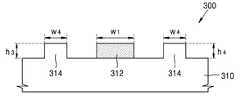
도 5에는 본 발명의 다른 실시예에 따른 포토 마스크에 대한 개략적인 단면도가 개시되어 있다. 상기 도면은 포토 마스크(300)의 일 부분에 대한 것으로서, 다른 부분에 비하여 패턴의 밀도가 낮은 부분 즉, 포토 마스크(300)에서 고립 패턴(312)이 형성되어 있는 영역이다. 도 5를 참조하면, 포토 마스크(300)는 첫 번째 실시예에 마찬가지로 투명 기판(310), 주 패턴(312) 및 스캐터링 바아(314)를 포함하는데, 본 실시예에 따르면 스캐터링 바아(314)는 투명 기판(310)을 식각하여 형성한다. 다만, 본 실시예에 의한 포토 마스크(300)는 스캐터링 바아(314)가 투명 기판(310)과 주 패턴(312)의 경계면에 대하여 돌출되어 있는 볼록형 패턴이라는 점에서 제1 실시예의 포토 마스크(200)와 상이하다.5 is a schematic cross-sectional view of a photo mask according to another embodiment of the present invention. The drawing is for a portion of the
도 5를 참조하면, 스캐터링 바아(314)는 소정의 폭(w4)과 높이(h4)를 가지는데, 상기 폭(w4)과 높이(h4)도 스캐터링 바아(314)를 통과한 광과 주 패턴(312)을 전사하는 광의 위상 차이가 180°보다 작게 되도록 하는, 폭과 높이를 갖는다. 이것은 스캐터링 바아(314)를 통과한 광과 주 패턴(312)을 전사하는 광이 완화된 간섭 효과를 일으키도록 하기 위해서 이다. 그 결과, 입사광의 에어리얼 이미지의 NILS값이 증가한다.Referring to FIG. 5, the
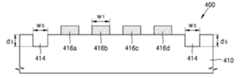
도 6에는 본 발명의 제3 실시예에 따른 포토 마스크(400)에 대한 개략적인 단면도가 도시되어 있다. 상기 도면은 포토 마스크(400)의 일 부분에 대한 것으로서, 다른 부분에 비하여 패턴의 밀도가 높은 부분 즉, 포토 마스크(400)에서 밀집 패턴(416a 내지 416d)이 형성되어 있는 영역이다. 도 6을 참조하면, 포토 마스크(400)는 첫 번째 실시예에 마찬가지로 투명 기판(410), 다수의 주 패턴(416a 내지 416d) 및 스캐터링 바아(414)를 포함한다. 도 6에서는 주 패턴(416a 내지 416d)이 4개만 도시되어 있지만, 상기 주 패턴(416a 내지 416d)의 개수에는 특별한 제한이 없다. 그리고, 본 실시예에 따르면 스캐터링 바아(414)도 투명 기판(410)을 식각하여 형성한다는 점에서 전술한 실시예와 동일하다. 다만, 본 실시예에 의한 포토 마스크(400)는 스캐터링 바아(414)가 주 패턴(416a 내지 416d) 중에서 가장자리에 위치하는 주 패턴(416a 및 416d)의 바깥쪽에만 형성되어 있다는 점에서, 전술한 실시예와 다르다.6 is a schematic cross-sectional view of a
도 6을 참조하면, 스캐터링 바아(414)는 소정의 폭(w5)과 깊이(d5)를 가지는데, 상기 폭(w5)과 깊이(h5)도 스캐터링 바아(414)를 통과한 광과 주 패턴(416a 내지 416d)을 전사하는 광의 위상 차이가 180°보다 작게 되도록 하는, 폭과 깊이를 갖는다. 이것은 스캐터링 바아(414)를 통과한 광과 주 패턴(416a 내지 416d)을 전사하는 광이 완화된 간섭 효과를 일으키도록 하기 위해서 이다. 그 결과, 입사광의 에어리얼 이미지의 NILS값이 증가한다.Referring to FIG. 6, the
본 발명에 의한 포토 마스크는 고립 패턴의 양 측면이나 밀집 패턴의 가장자리에 스캐터링 바아가 형성되어 있기 때문에, 노광 공정에서의 초점 심도를 증가시킬 수 있고, 패턴의 밀도에 따른 패턴 CD의 변이를 최소화시킬 수가 있다.In the photomask according to the present invention, since scattering bars are formed at both sides of the isolation pattern and at the edges of the dense pattern, the depth of focus in the exposure process can be increased, and the variation of the pattern CD according to the density of the pattern is minimized. I can do it.
그리고, 본 발명에 의한 포토 마스크는 투명 기판을 식각하여 스캐터링 바아를 형성한다. 따라서, 디자인 룰의 감소로 스캐터링 바아의 임계 치수가 더욱 미세화되는 경우에도, 포토 마스크의 스캐터링 바아가 옆으로 쓰러질 염려는 없다.In the photomask according to the present invention, the transparent substrate is etched to form a scattering bar. Thus, even if the critical dimension of the scattering bar is further refined due to the reduction of the design rule, there is no fear that the scattering bar of the photo mask will fall sideways.
뿐만 아니라, 투명 기판을 식각하여 스캐터링 바아를 형성하게 되면, 그 폭을 종래의 스캐터링 바아에 비하여 더 크게 만들 수 있기 때문에, 종래와 같이 해상도의 한계에 따른 제한을 받지 않고 제조 공정이 용이하다.In addition, when the scattering bar is formed by etching the transparent substrate, the width of the scattering bar can be made larger than that of the conventional scattering bar, so that the manufacturing process is easy without being limited by the limitation of resolution as in the prior art. .
Claims (20)
Translated fromKoreanPriority Applications (2)
| Application Number | Priority Date | Filing Date | Title |
|---|---|---|---|
| KR1020040008937AKR100585127B1 (en) | 2004-02-11 | 2004-02-11 | Photomask comprising a scattering bar formed on a transparent substrate |
| US11/051,461US20050175907A1 (en) | 2004-02-11 | 2005-02-07 | Photo mask including scattering bars and method of manufacturing the same |
Applications Claiming Priority (1)
| Application Number | Priority Date | Filing Date | Title |
|---|---|---|---|
| KR1020040008937AKR100585127B1 (en) | 2004-02-11 | 2004-02-11 | Photomask comprising a scattering bar formed on a transparent substrate |
Publications (2)
| Publication Number | Publication Date |
|---|---|
| KR20050080819A KR20050080819A (en) | 2005-08-18 |
| KR100585127B1true KR100585127B1 (en) | 2006-06-01 |
Family
ID=34825166
Family Applications (1)
| Application Number | Title | Priority Date | Filing Date |
|---|---|---|---|
| KR1020040008937AExpired - Fee RelatedKR100585127B1 (en) | 2004-02-11 | 2004-02-11 | Photomask comprising a scattering bar formed on a transparent substrate |
Country Status (2)
| Country | Link |
|---|---|
| US (1) | US20050175907A1 (en) |
| KR (1) | KR100585127B1 (en) |
Families Citing this family (7)
| Publication number | Priority date | Publication date | Assignee | Title |
|---|---|---|---|---|
| KR101068321B1 (en) | 2008-12-19 | 2011-09-28 | 주식회사 하이닉스반도체 | Vulnerability Point Detection Method |
| CN110119065B (en)* | 2018-02-06 | 2022-08-26 | 中芯国际集成电路制造(天津)有限公司 | Graph optimization method and mask preparation method |
| US11099478B2 (en)* | 2018-08-14 | 2021-08-24 | Taiwan Semiconductor Manufacturing Co., Ltd. | Photomask having recessed region |
| CN109148271B (en)* | 2018-08-17 | 2020-11-27 | 京东方科技集团股份有限公司 | Method for preparing a display substrate, display substrate and display screen |
| CN112946995B (en)* | 2019-12-10 | 2024-10-25 | 中芯国际集成电路制造(上海)有限公司 | Mask and method for forming semiconductor structure |
| CN112882339A (en)* | 2021-01-19 | 2021-06-01 | 泉芯集成电路制造(济南)有限公司 | Mask and preparation method thereof |
| CN119247684A (en)* | 2024-10-09 | 2025-01-03 | 重庆芯联微电子有限公司 | Mask and method for forming the same |
Family Cites Families (4)
| Publication number | Priority date | Publication date | Assignee | Title |
|---|---|---|---|---|
| TW447082B (en)* | 2000-09-07 | 2001-07-21 | United Microelectronics Corp | Method for increasing the line width window in a semiconductor process |
| KR100498441B1 (en)* | 2001-04-17 | 2005-07-01 | 삼성전자주식회사 | Mask for modifing optical proximity effect and method of manufacturing thereof |
| US7026081B2 (en)* | 2001-09-28 | 2006-04-11 | Asml Masktools B.V. | Optical proximity correction method utilizing phase-edges as sub-resolution assist features |
| KR100467323B1 (en)* | 2002-09-23 | 2005-01-24 | 한국전자통신연구원 | Optimization method and apparatus of decision level of output signal in optical receiver |
- 2004
- 2004-02-11KRKR1020040008937Apatent/KR100585127B1/ennot_activeExpired - Fee Related
- 2005
- 2005-02-07USUS11/051,461patent/US20050175907A1/ennot_activeAbandoned
Also Published As
| Publication number | Publication date |
|---|---|
| KR20050080819A (en) | 2005-08-18 |
| US20050175907A1 (en) | 2005-08-11 |
Similar Documents
| Publication | Publication Date | Title |
|---|---|---|
| CN106133599A (en) | Mask blank, phase-shifted mask and manufacture method thereof | |
| US5958656A (en) | Pattern forming method using phase shift mask | |
| US20100321656A1 (en) | Transmission mask with differential attenuation to improve iso-dense proximity | |
| KR101837247B1 (en) | Photomask, the method of manufacturing photomask, photomask blank and the method of manufacturing display device | |
| KR20100007387A (en) | Mask and method for manufacturing the same | |
| KR100585127B1 (en) | Photomask comprising a scattering bar formed on a transparent substrate | |
| CN102073224B (en) | Pattern formation method using levenson-type mask and method of manufacturing levenson-type mask | |
| JPH03141354A (en) | Exposing mask | |
| KR100732749B1 (en) | Mask for fine pattern formation | |
| JP2924804B2 (en) | Photomask, method of manufacturing the same, and photomask blanks | |
| US6861182B2 (en) | Tri-tone attenuated phase shift trim mask for double exposure alternating phase shift mask process | |
| US7033947B2 (en) | Dual trench alternating phase shift mask fabrication | |
| JP4574343B2 (en) | Phase shift mask and pattern forming method | |
| US6277528B1 (en) | Method to change transmittance of attenuated phase-shifting masks | |
| US7445159B2 (en) | Dual trench alternating phase shift mask fabrication | |
| KR100937660B1 (en) | Photomask with scattering bar | |
| US20080274414A1 (en) | High-transmission attenuating psm | |
| KR100498442B1 (en) | Photomask set and manufacturing method of the same | |
| JP4655532B2 (en) | Method for manufacturing exposure mask | |
| KR100811253B1 (en) | Manufacturing method of photo mask | |
| KR100861361B1 (en) | Photomasks and Manufacturing Methods | |
| JP2003121981A (en) | Mask and its manufacturing method and exposing method | |
| KR20120007978A (en) | Method of manufacturing lithographic mask and semiconductor device | |
| KR20090106873A (en) | Pattern formation method of semiconductor device | |
| JP2000214572A (en) | Photomask and exposure apparatus having the same |
Legal Events
| Date | Code | Title | Description |
|---|---|---|---|
| A201 | Request for examination | ||
| PA0109 | Patent application | St.27 status event code:A-0-1-A10-A12-nap-PA0109 | |
| PA0201 | Request for examination | St.27 status event code:A-1-2-D10-D11-exm-PA0201 | |
| R17-X000 | Change to representative recorded | St.27 status event code:A-3-3-R10-R17-oth-X000 | |
| PN2301 | Change of applicant | St.27 status event code:A-3-3-R10-R13-asn-PN2301 St.27 status event code:A-3-3-R10-R11-asn-PN2301 | |
| PN2301 | Change of applicant | St.27 status event code:A-3-3-R10-R13-asn-PN2301 St.27 status event code:A-3-3-R10-R11-asn-PN2301 | |
| PG1501 | Laying open of application | St.27 status event code:A-1-1-Q10-Q12-nap-PG1501 | |
| E902 | Notification of reason for refusal | ||
| PE0902 | Notice of grounds for rejection | St.27 status event code:A-1-2-D10-D21-exm-PE0902 | |
| E13-X000 | Pre-grant limitation requested | St.27 status event code:A-2-3-E10-E13-lim-X000 | |
| P11-X000 | Amendment of application requested | St.27 status event code:A-2-2-P10-P11-nap-X000 | |
| P13-X000 | Application amended | St.27 status event code:A-2-2-P10-P13-nap-X000 | |
| E701 | Decision to grant or registration of patent right | ||
| PE0701 | Decision of registration | St.27 status event code:A-1-2-D10-D22-exm-PE0701 | |
| GRNT | Written decision to grant | ||
| PR0701 | Registration of establishment | St.27 status event code:A-2-4-F10-F11-exm-PR0701 | |
| PR1002 | Payment of registration fee | St.27 status event code:A-2-2-U10-U11-oth-PR1002 Fee payment year number:1 | |
| PG1601 | Publication of registration | St.27 status event code:A-4-4-Q10-Q13-nap-PG1601 | |
| PR1001 | Payment of annual fee | St.27 status event code:A-4-4-U10-U11-oth-PR1001 Fee payment year number:4 | |
| PR1001 | Payment of annual fee | St.27 status event code:A-4-4-U10-U11-oth-PR1001 Fee payment year number:5 | |
| PR1001 | Payment of annual fee | St.27 status event code:A-4-4-U10-U11-oth-PR1001 Fee payment year number:6 | |
| PR1001 | Payment of annual fee | St.27 status event code:A-4-4-U10-U11-oth-PR1001 Fee payment year number:7 | |
| R18-X000 | Changes to party contact information recorded | St.27 status event code:A-5-5-R10-R18-oth-X000 | |
| FPAY | Annual fee payment | Payment date:20130430 Year of fee payment:8 | |
| PR1001 | Payment of annual fee | St.27 status event code:A-4-4-U10-U11-oth-PR1001 Fee payment year number:8 | |
| FPAY | Annual fee payment | Payment date:20140430 Year of fee payment:9 | |
| PR1001 | Payment of annual fee | St.27 status event code:A-4-4-U10-U11-oth-PR1001 Fee payment year number:9 | |
| LAPS | Lapse due to unpaid annual fee | ||
| PC1903 | Unpaid annual fee | St.27 status event code:A-4-4-U10-U13-oth-PC1903 Not in force date:20150525 Payment event data comment text:Termination Category : DEFAULT_OF_REGISTRATION_FEE | |
| PC1903 | Unpaid annual fee | St.27 status event code:N-4-6-H10-H13-oth-PC1903 Ip right cessation event data comment text:Termination Category : DEFAULT_OF_REGISTRATION_FEE Not in force date:20150525 | |
| P22-X000 | Classification modified | St.27 status event code:A-4-4-P10-P22-nap-X000 |