KR100582598B1 - LCD to prevent light leakage - Google Patents
LCD to prevent light leakageDownload PDFInfo
- Publication number
- KR100582598B1 KR100582598B1KR1020000062804AKR20000062804AKR100582598B1KR 100582598 B1KR100582598 B1KR 100582598B1KR 1020000062804 AKR1020000062804 AKR 1020000062804AKR 20000062804 AKR20000062804 AKR 20000062804AKR 100582598 B1KR100582598 B1KR 100582598B1
- Authority
- KR
- South Korea
- Prior art keywords
- liquid crystal
- display area
- pixel electrode
- substrate
- black matrix
- Prior art date
- Legal status (The legal status is an assumption and is not a legal conclusion. Google has not performed a legal analysis and makes no representation as to the accuracy of the status listed.)
- Expired - Lifetime
Links
Images


Classifications
- G—PHYSICS
- G02—OPTICS
- G02F—OPTICAL DEVICES OR ARRANGEMENTS FOR THE CONTROL OF LIGHT BY MODIFICATION OF THE OPTICAL PROPERTIES OF THE MEDIA OF THE ELEMENTS INVOLVED THEREIN; NON-LINEAR OPTICS; FREQUENCY-CHANGING OF LIGHT; OPTICAL LOGIC ELEMENTS; OPTICAL ANALOGUE/DIGITAL CONVERTERS
- G02F1/00—Devices or arrangements for the control of the intensity, colour, phase, polarisation or direction of light arriving from an independent light source, e.g. switching, gating or modulating; Non-linear optics
- G02F1/01—Devices or arrangements for the control of the intensity, colour, phase, polarisation or direction of light arriving from an independent light source, e.g. switching, gating or modulating; Non-linear optics for the control of the intensity, phase, polarisation or colour
- G02F1/13—Devices or arrangements for the control of the intensity, colour, phase, polarisation or direction of light arriving from an independent light source, e.g. switching, gating or modulating; Non-linear optics for the control of the intensity, phase, polarisation or colour based on liquid crystals, e.g. single liquid crystal display cells
- G02F1/133—Constructional arrangements; Operation of liquid crystal cells; Circuit arrangements
- G02F1/1333—Constructional arrangements; Manufacturing methods
- G02F1/1335—Structural association of cells with optical devices, e.g. polarisers or reflectors
- G02F1/133509—Filters, e.g. light shielding masks
- G02F1/133512—Light shielding layers, e.g. black matrix
- G—PHYSICS
- G02—OPTICS
- G02F—OPTICAL DEVICES OR ARRANGEMENTS FOR THE CONTROL OF LIGHT BY MODIFICATION OF THE OPTICAL PROPERTIES OF THE MEDIA OF THE ELEMENTS INVOLVED THEREIN; NON-LINEAR OPTICS; FREQUENCY-CHANGING OF LIGHT; OPTICAL LOGIC ELEMENTS; OPTICAL ANALOGUE/DIGITAL CONVERTERS
- G02F1/00—Devices or arrangements for the control of the intensity, colour, phase, polarisation or direction of light arriving from an independent light source, e.g. switching, gating or modulating; Non-linear optics
- G02F1/01—Devices or arrangements for the control of the intensity, colour, phase, polarisation or direction of light arriving from an independent light source, e.g. switching, gating or modulating; Non-linear optics for the control of the intensity, phase, polarisation or colour
- G02F1/13—Devices or arrangements for the control of the intensity, colour, phase, polarisation or direction of light arriving from an independent light source, e.g. switching, gating or modulating; Non-linear optics for the control of the intensity, phase, polarisation or colour based on liquid crystals, e.g. single liquid crystal display cells
- G02F1/133—Constructional arrangements; Operation of liquid crystal cells; Circuit arrangements
- G02F1/136—Liquid crystal cells structurally associated with a semi-conducting layer or substrate, e.g. cells forming part of an integrated circuit
- G—PHYSICS
- G02—OPTICS
- G02F—OPTICAL DEVICES OR ARRANGEMENTS FOR THE CONTROL OF LIGHT BY MODIFICATION OF THE OPTICAL PROPERTIES OF THE MEDIA OF THE ELEMENTS INVOLVED THEREIN; NON-LINEAR OPTICS; FREQUENCY-CHANGING OF LIGHT; OPTICAL LOGIC ELEMENTS; OPTICAL ANALOGUE/DIGITAL CONVERTERS
- G02F1/00—Devices or arrangements for the control of the intensity, colour, phase, polarisation or direction of light arriving from an independent light source, e.g. switching, gating or modulating; Non-linear optics
- G02F1/01—Devices or arrangements for the control of the intensity, colour, phase, polarisation or direction of light arriving from an independent light source, e.g. switching, gating or modulating; Non-linear optics for the control of the intensity, phase, polarisation or colour
- G02F1/13—Devices or arrangements for the control of the intensity, colour, phase, polarisation or direction of light arriving from an independent light source, e.g. switching, gating or modulating; Non-linear optics for the control of the intensity, phase, polarisation or colour based on liquid crystals, e.g. single liquid crystal display cells
- G02F1/133—Constructional arrangements; Operation of liquid crystal cells; Circuit arrangements
- G02F1/1333—Constructional arrangements; Manufacturing methods
- G02F1/133388—Constructional arrangements; Manufacturing methods with constructional differences between the display region and the peripheral region
Landscapes
- Physics & Mathematics (AREA)
- Nonlinear Science (AREA)
- Mathematical Physics (AREA)
- Chemical & Material Sciences (AREA)
- Crystallography & Structural Chemistry (AREA)
- General Physics & Mathematics (AREA)
- Optics & Photonics (AREA)
- Liquid Crystal (AREA)
- Engineering & Computer Science (AREA)
- Microelectronics & Electronic Packaging (AREA)
- Devices For Indicating Variable Information By Combining Individual Elements (AREA)
Abstract
Translated fromKoreanDescription
Translated fromKorean도 1은 일반적인 액정패널의 단면을 도시한 단면도.1 is a cross-sectional view showing a cross section of a general liquid crystal panel.
도 2는 일반적인 액정표시장치에 있어서, 표시영역과 비표시 영역을 포함하는 하부기판의 일부 영역에 해당하는 평면도.2 is a plan view of a portion of a lower substrate including a display area and a non-display area in a general liquid crystal display device;
도 3은 도 2의 절단선 A-A'에 따른 상, 하부 기판의 단면도.3 is a cross-sectional view of the upper and lower substrates along the cutting line A-A 'of FIG.
도 4는 본 발명의 액정표시장치에 있어서, 블랙 매트릭스 영역이 표시된 표시영역과 비표시 영역을 포함하는 하부기판의 일부 영역에 해당하는 평면도.4 is a plan view of a partial region of a lower substrate including a display area in which a black matrix area is displayed and a non-display area in the liquid crystal display of the present invention;
도 5는 도 4의 절단선 B-B'에 따른 상, 하부 기판의 단면도.5 is a cross-sectional view of the upper and lower substrates taken along the line BB ′ ′ of FIG. 4.
< 도면의 주요 부분에 대한 부호의 설명 ><Description of Symbols for Main Parts of Drawings>
100 : 하부기판 110 : 비표시 영역100: lower substrate 110: non-display area
120 : 표시영역 142 : 게이트 배선120: display area 142: gate wiring
144 : 데이터 배선 146a : 제 1 화소전극144:
146b : 제 2 화소전극 146 : 화소전극146b: second pixel electrode 146: pixel electrode
L2 : 블랙 매트릭스에 의해 가려지는 제 1 화소전극 영역L2 : first pixel electrode region covered by the black matrix
BM : 표시영역 가장자리의 블랙 매트릭스 영역BM : Black matrix area at the edge of the display area
RD : 러빙방향RD : rubbing direction
본 발명은 액정표시장치에 관한 것으로, 좀더 상세하게는 빛샘 현상을 방지하는 액정표시장치에 관한 것이다.The present invention relates to a liquid crystal display device, and more particularly, to a liquid crystal display device for preventing light leakage phenomenon.
액정표시장치의 구동원리는 액정의 광학적 이방성과 분극성질을 이용한다. 상기 액정은 구조가 가늘고 길기 때문에 분자의 배열에 방향성을 갖고 있으며, 인위적으로 액정에 전기장을 인가하여 분자배열의 방향을 제어할 수 있다.The driving principle of the liquid crystal display device uses the optical anisotropy and polarization property of the liquid crystal. Since the liquid crystal is thin and long in structure, the liquid crystal has directivity in the arrangement of molecules, and the direction of the molecular arrangement can be controlled by artificially applying an electric field to the liquid crystal.
따라서, 상기 액정의 분자배열 방향을 임의로 조절하면, 액정의 분자배열이 변하게 되고, 광학적 이방성에 의하여 상기 액정의 분자 배열 방향으로 빛이 굴절하여 화상정보를 표현할 수 있다.Accordingly, when the molecular arrangement direction of the liquid crystal is arbitrarily adjusted, the molecular arrangement of the liquid crystal is changed, and light is refracted in the molecular arrangement direction of the liquid crystal due to optical anisotropy to express image information.
현재에는 스위칭 소자인 박막 트랜지스터와 이 박막 트랜지스터에 연결된 화소전극이 행렬 방식으로 배열된 능동행렬 액정표시장치(Active Matrix LCD : AM-LCD)가 해상도 및 동영상 구현능력이 우수하여 가장 주목받고 있다.Currently, active matrix LCDs (AM-LCDs) in which a thin film transistor, which is a switching element, and pixel electrodes connected to the thin film transistor are arranged in a matrix manner, are attracting the most attention due to their excellent resolution and ability to implement video.
일반적으로 액정표시장치를 구성하는 기본적인 부품인 액정패널의 구조를 살 펴보면 다음과 같다.In general, the structure of a liquid crystal panel, which is a basic component of a liquid crystal display, will be described.
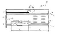
도 1은 일반적인 액정패널의 단면을 도시한 단면도이다.1 is a cross-sectional view showing a cross section of a general liquid crystal panel.
상기 액정패널(20)은 컬러필터 기판인 상부기판(4)과 어레이 기판인 하부기판(2)과, 이 상, 하부기판(4, 2) 사이에 충진된 액정층(10)으로 구성된다.The
이 상부기판(4)의 투명기판(1)의 하부에는, 특정 파장대의 빛만을 투과하고 나머지 빛은 흡수하는 R,G,B셀(8a)과 R,G,B셀(8a) 간의 갭을 조절하고 하부기판(2)의 액정구동 영역을 제외한 부분에서의 빛의 차단 및 박막 트랜지스터로의 빛 조사를 방지하는 블랙 매트릭스(8b)로 이루어진 컬러필터(8)가 위치하고 있다.Under the
이 컬러필터(8)의 하부에는 액정에 전압을 인가하는 한쪽 전극역할을 하는 공통전극(9)이 위치하고 있다.Below the
상기 하부기판(2)의 투명기판(1)의 상부에는 스위칭 역할을 하는 박막 트랜지스터(T)와 이 박막 트랜지스터(T)로부터 신호를 인가 받고 상기 액정층(10)으로 전압을 인가하는 다른 한쪽의 전극역할을 하는 화소전극(14)이 형성되어 있다.The thin film transistor T, which serves as a switching role, and the other side that receives a signal from the thin film transistor T and applies a voltage to the
상기 화소전극(14)이 형성된 부분을 화소부(P)라고 한다.The portion where the
또한, 상기 상, 하부기판(4, 2)에는 상기 액정층(10)과의 접촉면에 각각 전압 인가시 액정의 배향을 용이하게 해주는 상, 하부 배향막(5,11)이 형성되어 있다.In addition, upper and
그리고, 상기 상, 하부기판(4, 2) 사이에 충진된 액정층(10)의 누설을 방지하기 위해, 상기 상, 하부기판(4, 2)의 가장자리는 실런트(sealant : 6)로 봉인되어 있다.In order to prevent leakage of the
상기 하부기판은 상부기판에 비해 다수의 공정을 거쳐 제작되며, 상기 하부기 판을 어레이 기판으로 제작하는데는, 증착(deposition), 포토리소그라피(photolithography) 공정이 여러 번 반복되어서 화소부(P)를 제외한 영역에는 다수개의 어레이 소자들이 단차를 이루게 되므로, 상부기판에 비해 단차빈도가 높게 된다.The lower substrate is manufactured through a plurality of processes compared to the upper substrate, and the lower substrate is manufactured as an array substrate, and the pixel portion P is repeatedly formed by repeatedly performing deposition and photolithography processes. Since the plurality of array elements form a step in the excluded region, the step frequency is higher than that of the upper substrate.
도 2는 일반적인 액정표시장치에 있어서, 표시영역과 비표시 영역을 포함하는 하부기판의 일부 영역에 해당하는 평면도이다.FIG. 2 is a plan view of a portion of a lower substrate including a display area and a non-display area in a general liquid crystal display device.
이 액정표시장치용 하부기판은 화면구현 영역인 표시영역과 상, 하부기판의 합착을 위한 기준점이 되는 합착키(alignment key) 및 액정패널의 전기적 검사를 위한 단락배선(short circuit bar)이 형성된 비표시 영역으로 구분된다.The lower substrate for the liquid crystal display device has a ratio in which an alignment key, which is a reference point for bonding the upper and lower substrates, with the display area, which is a screen realization region, and a short circuit bar for electrical inspection of the liquid crystal panel, are formed. It is divided into display areas.
이 비표시 영역은 합착 및 전기검사 공정이 완료되면, 커팅되어 폐기된다.This non-display area is cut and discarded when the bonding and electrical inspection processes are completed.
도시한 바와 같이, 액정표시장치용 하부기판(2)은 표시영역(40)과 비표시 영역(30)으로 구분된다.As shown, the
이 하부기판(2)의 표시영역(40) 상에는 가로방향으로 형성된 다수개의 게이트 배선(42)과 이 게이트 배선(42)과 직교하는 데이터 배선(44)이 다수개 형성되어 있다.On the
이 게이트 배선(42)과 데이터 배선(44)이 교차하는 영역에는 다수개의 화소전극(46)이 매트릭스(matrix)로 형성되어 있다.In the region where the
그리고, 이 화소전극(46)과 전기적으로 연결된 박막 트랜지스터(T)가 형성되어 있다.Then, a thin film transistor T electrically connected to the
이후 기술될 내용설명의 편의상 상기 표시영역(40)과 인접한 화소전극(46)을 제 1 화소전극(46a)이라고 하고, 이 제 1 화소전극(46a)보다 기판의 안쪽에 위치하는 화소전극(46)을 제 2 화소전극(46b)으로 칭하겠다.For convenience of description, hereinafter, the
도면 우측의 화살표는 미도시한 액정 배향막의 러빙(rubbing)방향(RD)을 나타내는 것으로, 일반적으로 기판에 러빙처리시, 기판의 가장자리 부분에서는 기판의 어레이 소자들의 단차로 인해 러빙이 불균일하게 이루어지기 쉽다.The arrow on the right side of the drawing indicates the rubbing direction RD of the liquid crystal alignment layer, which is not shown. In general, when rubbing is performed on a substrate, rubbing becomes uneven due to a step difference between array elements of the substrate. Easy to lose
특히, 상기와 같이 기판의 아래에서 윗방향으로 러빙처리시, 기판의 왼쪽과 오른쪽 가장자리부분에서 러빙이 불균일이 가장 심하게 나타나게 되고, 이러한 현상은 상, 하부 기판 합착 후 액정구동시 화면의 가장자리 부근의 빛샘현상의 원인이 된다.In particular, when the rubbing process from the bottom of the substrate to the upper direction as described above, rubbing occurs most severely at the left and right edges of the substrate, and this phenomenon occurs when the liquid crystal is driven after the upper and lower substrates are bonded. It causes light leakage.
도 3은 도 2의 절단선 A-A'에 따른 상, 하부기판의 단면도로서, 표시영역의 경계선에 인접한 화소부에 대한 것이다.FIG. 3 is a cross-sectional view of the upper and lower substrates along the cutting line A-A 'of FIG. 2 and is for the pixel portion adjacent to the boundary line of the display area.
상기 도면은 도 1에서 상술한 바와 같은 구조의 액정표시장치로서, 상기 하부기판(2)에는 제 1 화소전극(46a)과 데이터 배선(44)이 일정간격 이격되어 형성되어 있고, 상기 상부기판(4)의 블랙 매트릭스(8b)는 하부기판(2)상의 제 1 화소전극(46a)을 제외하고, 상기 데이터 배선(44)과 이 데이터 배선(44)과 제 1 화소전극(46a) 사이 구간과 대응하는 위치에 형성되어 있다.FIG. 1 is a liquid crystal display having a structure as described above with reference to FIG. 1, wherein the
그리고, 상기 상, 하부기판(4, 2)에는 액정층(10)과의 접촉면에 각각 상, 하부 배향막(5, 11)이 형성되어 있다.In the upper and
이러한 배향막을 이루는 대표적인 물질로는 폴리이미드(Polyimide) 수지를 들 수 있는데, 이 폴리이미드 수지는 그 자체가 액정분자를 평행배향시키는 기능을 가지고 있고, 대부분의 액정 물질에 양호한 배향효과를 나타내는 장점을 가지고 있다.Representative materials constituting the alignment layer include a polyimide resin, which itself has a function of parallel alignment of liquid crystal molecules, and exhibits a good alignment effect on most liquid crystal materials. Have.
일반적으로 이러한 배향막에는 액정의 배향을 일정하게 하고, 액정의 배향을 용이하게 유도하기 위한 선경사각(pretilt angle)을 주기 위해 러빙처리를 하게 되는데, 이러한 러빙처리는 러빙포로 감싼 회전롤러를 기판과 일정한 각도를 유지하며 압력을 가하여 배향막에 일정한 홈을 형성하는 것으로, 이러한 과정에서 기판의 가장자리 부근에서는 러빙이 불균일하게 이루어지기 쉽다.In general, the alignment layer is subjected to a rubbing treatment to make the alignment of the liquid crystal constant and to give a pretilt angle for easily inducing the alignment of the liquid crystal. Forming a constant groove in the alignment layer by applying pressure while maintaining the angle, in this process rubbing tends to be uneven near the edge of the substrate.
이러한 현상은 상, 하부기판 중 특히 단차빈도가 높은 하부기판(2) 상에서 일어나기 쉽다.This phenomenon is likely to occur on the
즉, 상기 하부 배향막(11)의 러빙의 불균일은 표시영역 상에서 볼 때, 표시영역의 경계선에 위치한 제 1 화소전극(46a)상에 러빙불균일 영역(R)이 발생하게 되고, 이러한 R영역 상의 액정(15)의 배열은 흩트러지게 되고, 이러한 현상은 빛샘현상을 유발하게 된다.That is, when the rubbing unevenness of the
상기 러빙의 불균일한 영역(R)은 특히 러빙방향에 따라 그 정도의 차이가 달라질 수 있다.The non-uniform area R of the rubbing may vary in particular depending on the rubbing direction.
예를 들어, TN(twist nematic)액정모드에서는 상, 하부기판을 대각선방향으로 서로 직교하게 러빙처리를 하므로, 이럴 경우에도 하부기판의 대각선과 평행을 이루는 양쪽가장자리에서 러빙의 불균일이 심하게 발생할 수 있다.For example, in the TN (twist nematic) liquid crystal mode, the upper and lower substrates are rubbed at right angles to each other in a diagonal direction, so even in this case, uneven rubbing may occur at both edges parallel to the diagonals of the lower substrate. .
상술한 바와 같이, 일반적인 액정표시장치에서는 기판의 가장자리에서 러빙이 불균일하게 이루어지므로써, 표시영역의 경계선에 인접한 화소전극 상의 액정의 배향이 제대로 이루어지지 않아 화면 상에 빛샘현상이 발생되는 문제점이 있다.As described above, in a general liquid crystal display device, since rubbing is unevenly performed at the edge of the substrate, there is a problem in that light leakage occurs on the screen because the alignment of the liquid crystal on the pixel electrode adjacent to the boundary of the display area is not properly performed. .
이러한 문제점을 해결하기 위하여, 본 발명에서는 러빙이 불균일하게 이루어진 화소전극 영역에서의 빛을 차단하여 화질이 개선된 액정표시장치를 제공하는데 목적이 있다.
In order to solve this problem, an object of the present invention is to provide a liquid crystal display device having improved image quality by blocking light in a pixel electrode region in which rubbing is uneven.
상기 목적을 달성하기 위하여, 본 발명에서는 표시영역과 비표시 영역을 가지는 어레이 기판과; 상기 어레이 기판의 표시영역 상에 서로 교차하며 형성된 다수개의 게이트 배선 및 데이터 배선과; 상기 게이트 배선 및 데이터 배선이 교차되는 영역 상에 형성된 다수개의 화소전극과; 상기 화소전극과 전기적으로 연결되어 있는 박막 트랜지스터와; 상기 어레이 기판과 일정간격 이격되어 대향된 컬러필터 기판과; 상기 컬러필터 기판의 하부에, 표시영역의 경계선에 인접한 화소전극의 일부영역과 대응하는 위치에 형성된 블랙 매트릭스와; 상기 컬러필터 기판과 어레이 기판 사이에 충진된 액정층과; 상기 컬러필터 기판과 어레이 기판의 상기 액정층과의 접촉면에 각각 형성된 상, 하부 배향막을 포함하는 액정표시장치를 제공한다.In order to achieve the above object, the present invention is an array substrate having a display area and a non-display area; A plurality of gate lines and data lines intersecting each other on a display area of the array substrate; A plurality of pixel electrodes formed on an area where the gate line and the data line cross each other; A thin film transistor electrically connected to the pixel electrode; A color filter substrate facing and spaced apart from the array substrate at a predetermined interval; A black matrix formed below the color filter substrate at a position corresponding to a partial region of the pixel electrode adjacent to the boundary line of the display region; A liquid crystal layer filled between the color filter substrate and the array substrate; Provided is a liquid crystal display including upper and lower alignment layers formed on contact surfaces of the color filter substrate and the liquid crystal layer of the array substrate, respectively.
상기 배향막은 폴리이미드(Poly Imide)로 이루어진 유기물이며, 상기 블랙 매트릭스는 표시영역 상의 전압 인가시 액정이 구동되지 않는 영역과 대응하는 위치 에 형성됨을 특징으로 한다.The alignment layer is an organic material made of polyimide, and the black matrix is formed at a position corresponding to a region where the liquid crystal is not driven when voltage is applied on the display region.
이하, 본 발명의 바람직한 실시예를 첨부한 도면을 참조하여 설명하기로 한다.Hereinafter, preferred embodiments of the present invention will be described with reference to the accompanying drawings.
도 4는 본 발명의 액정표시장치에 있어서, 표시영역과 비표시 영역을 포함하는 하부기판의 일부 영역에 해당하는 평면도이다.4 is a plan view of a partial region of a lower substrate including a display area and a non-display area in the liquid crystal display of the present invention.
도시한 바와 같이, 본 발명의 액정표시장치용 하부기판(100)은 표시영역(120)과 비표시 영역(110)으로 구분된다.As shown, the
이 하부기판(100)의 표시영역(120) 상에는 가로방향으로 형성된 다수개의 게이트 배선(142)과 이 게이트 배선(142)과 직교하며 다수개의 데이터 배선(144)이 형성되어 있다.On the
이 게이트 배선(142)과 데이터 배선(144)이 교차하는 영역으로 정의되는 화소부에는 표시영역(120)의 경계선에 인접한 제 1 화소전극(146a)과 이 제 1 화소전극(146a)보다 기판의 안쪽에 위치하는 제 2 화소전극(146b)으로 구성된 화소전극(146)이 형성되어 있다.In the pixel portion defined as the region where the
그리고, 이러한 화소전극(146)과 연결되어 박막 트랜지스터(T)가 형성되어 있다.The thin film transistor T is connected to the
이때, 도면상의 빗금친 영역은 표시영역(120)의 경계선과 제 1 화소전극(146a) 사이 구간의 미도시한 상부기판의 블랙 매트릭스의 형성영역을 나타낸 것으로, 이 영역(BM)은 특히, 표시영역(120)의 경계선과 인접한 제 1 화소전극(146a)의 일부영역(L2)까지 포함 함을 특징으로 한다.In this case, the shaded region on the figure illustrates the forming region of the
이러한 영역(BM)은 러빙방향과 평행한 방향의 기판의 가장자리부근이나 또는 기판의 가장자리 모두에 형성할 수 도 있다.Such an area BM may be formed near the edge of the substrate in the direction parallel to the rubbing direction, or both at the edge of the substrate.
상기와 같이 블랙 매트릭스 영역을 형성하는 이유는, 액정 배향막의 러빙처리시 기판의 가장자리부분에서 러빙이 불균일하게 되어, 표시영역의 경계선에 인접한 화소전극 일부영역 상의 액정배향이 불규칙하게 되어, 화면 상에 빛샘현상이 발생하므로, 이러한 현상을 차단하기 위하여, 상기 러빙이 불균일하게 처리된 화소전극의 일부영역까지 대응하도록 블랙 매트릭스를 형성하는 것이다.The reason for forming the black matrix region as described above is that the rubbing becomes uneven at the edges of the substrate during the rubbing treatment of the liquid crystal alignment layer, resulting in irregular liquid crystal alignment on the partial region of the pixel electrode adjacent to the boundary of the display region, Since light leakage occurs, in order to block such a phenomenon, the black matrix is formed to correspond to a partial region of the pixel electrode in which the rubbing is unevenly processed.
도 5는 도 4의 절단선 B-B'에 따른 상, 하부 기판의 단면도로서, 표시영역의 경계선에 인접한 영역 상의 화소부에 대한 것이다.FIG. 5 is a cross-sectional view of the upper and lower substrates along the cutting line B-B 'of FIG. 4, and illustrates a pixel portion on an area adjacent to a boundary line of the display area.
도시한 바와 같이, 본 발명의 액정표시장치는 컬러필터 기판인 상부기판(200)과 어레이 기판인 하부기판(100)과 이 상, 하부기판(200, 100) 사이에 충진된 액정층(150)으로 이루어진다.As shown, the liquid crystal display device of the present invention is a
이 상, 하부 기판(200, 100)에는 상기 액정층(150)과의 접촉면에 각각 상, 하부 배향막(220, 111)이 형성되어 있으며, 상기 상부기판(200)에는 투명기판(1)과 상기 상부배향막(220) 사이에 블랙매트릭스(210)와 공통전극(230)이 형성된다.Upper and
이러한 배향막을 이루는 물질로는 폴리이미드(polyimide)를 주로 이용한다.As a material forming the alignment layer, polyimide is mainly used.
이 하부기판(100)의 투명기판(1) 상에는 제 1 화소전극(146a)과 데이터 배선(144)이 일정간격 이격되어 형성되어 있다.On the
이때, 이 제 1 화소전극(146a)은 하부기판(100)의 표시영역(120)의 경계선에 인접한 화소전극으로서, 특히 러빙이 불균일이 심하게 발생하는 영역이므로, 이러한 이유로 이러한 제 1 화소전극(146a)의 러빙이 불균일하게 이루어진 영역(R) 상의 액정은 전압 인가시, 배열이 흐트러져, 화면 상에 빛샘현상을 유발하게 되므로, 이러한 러빙 불균일 영역(R)과 대응하는 위치까지 상부기판(200)의 블랙 매트릭스(210)의 형성범위를 넓혔다.In this case, the
이때, 상기 블랙 매트릭스는 표시영역의 경계선에 인접한 화소전극을 제외한 나머지 영역에서는 일반적인 액정표시장치에서의 블랙 매트릭스의 형성범위와 동일하게 이루어진다. 다시 말해, 본 발명에 따른 액정표시장치는 상기 표시영역 중앙부에 형성되는 블랙매트릭스보다 상기 표시영역과 비표시영역의 경계선에 인접한 위치에 형성되는 블랙매트릭스가 화소전극을 더욱 많이 덮도록 형성된다.In this case, the black matrix has the same range as that of the black matrix in a general liquid crystal display device in the remaining regions except for the pixel electrode adjacent to the boundary of the display region. In other words, the LCD according to the present invention is formed such that the black matrix formed at a position adjacent to the boundary between the display area and the non-display area covers the pixel electrode more than the black matrix formed at the center of the display area.
이상과 같이, 본 발명의 액정표시장치에서는, 별도의 추가공정없이 블랙 매트릭스의 형성범위를 표시영역의 가장자리부근에서 넓힘으로써, 빛샘 현상을 방지하여, 화질의 저하를 방지할 수 있는 장점이 있다.As described above, in the liquid crystal display device of the present invention, the light matrix phenomenon can be prevented and the deterioration of image quality can be prevented by widening the formation range of the black matrix near the edge of the display area without any additional process.
Claims (6)
Translated fromKoreanPriority Applications (2)
| Application Number | Priority Date | Filing Date | Title |
|---|---|---|---|
| KR1020000062804AKR100582598B1 (en) | 2000-10-25 | 2000-10-25 | LCD to prevent light leakage |
| US09/983,445US7414681B2 (en) | 2000-10-25 | 2001-10-24 | Liquid crystal display device having black matrix covering periphery of display region |
Applications Claiming Priority (1)
| Application Number | Priority Date | Filing Date | Title |
|---|---|---|---|
| KR1020000062804AKR100582598B1 (en) | 2000-10-25 | 2000-10-25 | LCD to prevent light leakage |
Publications (2)
| Publication Number | Publication Date |
|---|---|
| KR20020031984A KR20020031984A (en) | 2002-05-03 |
| KR100582598B1true KR100582598B1 (en) | 2006-05-23 |
Family
ID=19695291
Family Applications (1)
| Application Number | Title | Priority Date | Filing Date |
|---|---|---|---|
| KR1020000062804AExpired - LifetimeKR100582598B1 (en) | 2000-10-25 | 2000-10-25 | LCD to prevent light leakage |
Country Status (2)
| Country | Link |
|---|---|
| US (1) | US7414681B2 (en) |
| KR (1) | KR100582598B1 (en) |
Families Citing this family (12)
| Publication number | Priority date | Publication date | Assignee | Title |
|---|---|---|---|---|
| JP4544809B2 (en) | 2001-07-18 | 2010-09-15 | 三星電子株式会社 | Liquid crystal display |
| KR100806896B1 (en)* | 2001-07-18 | 2008-02-22 | 삼성전자주식회사 | Liquid crystal display |
| US20070109468A1 (en)* | 2005-11-15 | 2007-05-17 | Toppoly Optoelectronics Corp. | Systems with reduced color lines at edges of associated display devices |
| JP2008224759A (en)* | 2007-03-08 | 2008-09-25 | Seiko Epson Corp | Active matrix circuit board and display device |
| KR101431154B1 (en)* | 2007-11-08 | 2014-08-18 | 삼성디스플레이 주식회사 | Display apparatus and method for assembling the same |
| KR101097341B1 (en)* | 2010-03-09 | 2011-12-23 | 삼성모바일디스플레이주식회사 | Organic light emitting display apparatus |
| US8582060B2 (en) | 2011-12-19 | 2013-11-12 | Japan Display West Inc. | Liquid crystal display panel |
| KR101965207B1 (en)* | 2012-03-27 | 2019-04-05 | 삼성디스플레이 주식회사 | Display apparatus |
| KR101455312B1 (en) | 2012-06-21 | 2014-10-27 | 엘지디스플레이 주식회사 | A Patterned Retarder Type Stereoscopic Image Display Device and Method for Manufacturing The Same |
| KR101425611B1 (en)* | 2012-07-04 | 2014-07-31 | 엘지디스플레이 주식회사 | A Patterned Retarder Type Stereoscopic Image Display Device and Method for Manufacturing The Same |
| CN104166273A (en)* | 2014-06-26 | 2014-11-26 | 京东方科技集团股份有限公司 | Display substrate, display substrate mother board and display device |
| CN111856806A (en)* | 2019-04-30 | 2020-10-30 | 群创光电股份有限公司 | display device |
Citations (2)
| Publication number | Priority date | Publication date | Assignee | Title |
|---|---|---|---|---|
| KR19980072227A (en)* | 1997-03-03 | 1998-11-05 | 구자홍 | LCD |
| KR100245973B1 (en)* | 1995-07-25 | 2000-03-02 | 가나이 쓰도무 | LCD and its manufacturing method |
Family Cites Families (17)
| Publication number | Priority date | Publication date | Assignee | Title |
|---|---|---|---|---|
| US5365357A (en)* | 1988-04-21 | 1994-11-15 | Asahi Glass Company Ltd. | Color liquid crystal display having color filters and light blocking layers in the periphery |
| JPH03296701A (en)* | 1990-04-13 | 1991-12-27 | Internatl Business Mach Corp <Ibm> | Color-filter and repairing method thereof and liquid-crystal display unit |
| KR960014823B1 (en)* | 1991-03-15 | 1996-10-21 | 가부시기가이샤 히다찌세이사구쇼 | LCD Display |
| KR940004322B1 (en)* | 1991-09-05 | 1994-05-19 | 삼성전자 주식회사 | Liquid crystal display devices |
| JP3172840B2 (en)* | 1992-01-28 | 2001-06-04 | 株式会社日立製作所 | Active matrix substrate manufacturing method and liquid crystal display device |
| EP1703317B1 (en)* | 1992-02-27 | 2008-08-06 | Canon Kabushiki Kaisha | Liquid crystal display device |
| JP2543286B2 (en)* | 1992-04-22 | 1996-10-16 | インターナショナル・ビジネス・マシーンズ・コーポレイション | Liquid crystal display |
| JP3526058B2 (en)* | 1992-08-19 | 2004-05-10 | セイコーインスツルメンツ株式会社 | Semiconductor device for light valve |
| JPH07271020A (en)* | 1994-03-18 | 1995-10-20 | Internatl Business Mach Corp <Ibm> | Photosensitive composition for forming black matrix, color filter substrate and liquid crystal display device using substrate thereof |
| JP3109979B2 (en)* | 1994-06-20 | 2000-11-20 | キヤノン株式会社 | Liquid crystal display |
| JPH0933874A (en)* | 1995-07-14 | 1997-02-07 | Sharp Corp | Liquid crystal display device and manufacturing method thereof |
| KR100228282B1 (en)* | 1996-09-17 | 1999-11-01 | 윤종용 | Liquid crystal display |
| JP3300638B2 (en)* | 1997-07-31 | 2002-07-08 | 株式会社東芝 | Liquid crystal display |
| TW520457B (en)* | 1997-09-30 | 2003-02-11 | Toshiba Corp | Display panel and position adjusting method for the display panel |
| US6433841B1 (en)* | 1997-12-19 | 2002-08-13 | Seiko Epson Corporation | Electro-optical apparatus having faces holding electro-optical material in between flattened by using concave recess, manufacturing method thereof, and electronic device using same |
| CN1195243C (en)* | 1999-09-30 | 2005-03-30 | 三星电子株式会社 | Film transistor array panel for liquid crystal display and its producing method |
| JP3813433B2 (en)* | 2000-10-16 | 2006-08-23 | 株式会社アドバンスト・ディスプレイ | Liquid crystal display |
- 2000
- 2000-10-25KRKR1020000062804Apatent/KR100582598B1/ennot_activeExpired - Lifetime
- 2001
- 2001-10-24USUS09/983,445patent/US7414681B2/ennot_activeExpired - Lifetime
Patent Citations (2)
| Publication number | Priority date | Publication date | Assignee | Title |
|---|---|---|---|---|
| KR100245973B1 (en)* | 1995-07-25 | 2000-03-02 | 가나이 쓰도무 | LCD and its manufacturing method |
| KR19980072227A (en)* | 1997-03-03 | 1998-11-05 | 구자홍 | LCD |
Also Published As
| Publication number | Publication date |
|---|---|
| US20020054253A1 (en) | 2002-05-09 |
| US7414681B2 (en) | 2008-08-19 |
| KR20020031984A (en) | 2002-05-03 |
Similar Documents
| Publication | Publication Date | Title |
|---|---|---|
| KR100255584B1 (en) | Active matrix liquid crystal display and manufacturing method | |
| JP3850002B2 (en) | Liquid crystal electro-optical device | |
| JP3066255B2 (en) | Liquid crystal display | |
| KR100582598B1 (en) | LCD to prevent light leakage | |
| KR100959367B1 (en) | Transverse electric field type liquid crystal display device | |
| KR100789086B1 (en) | In-Plane Switching mode Liquid Crystal Display Device | |
| US8009254B2 (en) | Bend alignment type liquid crystal display apparatus | |
| JP3796115B2 (en) | Liquid crystal display | |
| US6097463A (en) | Liquid crystal display device | |
| KR100293431B1 (en) | In-plane switching mode liquid crystal display device | |
| KR20060080129A (en) | Liquid crystal display | |
| KR100903650B1 (en) | Liquid crystal display | |
| JP4019906B2 (en) | Liquid crystal display | |
| KR100577299B1 (en) | LCD Display | |
| KR101048701B1 (en) | Manufacturing method of color filter substrate | |
| KR20090036870A (en) | LCD Display | |
| JPH11264969A (en) | Liquid crystal display | |
| US7268847B2 (en) | In-plane switching mode thin film transistor liquid crystal display device with two domains | |
| KR100984348B1 (en) | Multi-domain liquid crystal display device and thin film transistor display panel thereof | |
| KR101001490B1 (en) | LCD Display | |
| KR20080057409A (en) | LCD Display | |
| KR20030033833A (en) | Multi-domain Liquid Crystal Display Device And Method For Fabricating The Same | |
| KR101027866B1 (en) | LCD Display | |
| KR100483524B1 (en) | Liquid crystal display device with uniform substrate spacing and manufacturing method | |
| KR101233728B1 (en) | Liquid crystal display device |
Legal Events
| Date | Code | Title | Description |
|---|---|---|---|
| PA0109 | Patent application | Patent event code:PA01091R01D Comment text:Patent Application Patent event date:20001025 | |
| PG1501 | Laying open of application | ||
| A201 | Request for examination | ||
| PA0201 | Request for examination | Patent event code:PA02012R01D Patent event date:20040416 Comment text:Request for Examination of Application Patent event code:PA02011R01I Patent event date:20001025 Comment text:Patent Application | |
| E902 | Notification of reason for refusal | ||
| PE0902 | Notice of grounds for rejection | Comment text:Notification of reason for refusal Patent event date:20051117 Patent event code:PE09021S01D | |
| E701 | Decision to grant or registration of patent right | ||
| PE0701 | Decision of registration | Patent event code:PE07011S01D Comment text:Decision to Grant Registration Patent event date:20060515 | |
| GRNT | Written decision to grant | ||
| PR0701 | Registration of establishment | Comment text:Registration of Establishment Patent event date:20060516 Patent event code:PR07011E01D | |
| PR1002 | Payment of registration fee | Payment date:20060517 End annual number:3 Start annual number:1 | |
| PG1601 | Publication of registration | ||
| PR1001 | Payment of annual fee | Payment date:20090323 Start annual number:4 End annual number:4 | |
| PR1001 | Payment of annual fee | Payment date:20100318 Start annual number:5 End annual number:5 | |
| PR1001 | Payment of annual fee | Payment date:20110329 Start annual number:6 End annual number:6 | |
| FPAY | Annual fee payment | Payment date:20120330 Year of fee payment:7 | |
| PR1001 | Payment of annual fee | Payment date:20120330 Start annual number:7 End annual number:7 | |
| FPAY | Annual fee payment | Payment date:20130329 Year of fee payment:8 | |
| PR1001 | Payment of annual fee | Payment date:20130329 Start annual number:8 End annual number:8 | |
| FPAY | Annual fee payment | Payment date:20150429 Year of fee payment:10 | |
| PR1001 | Payment of annual fee | Payment date:20150429 Start annual number:10 End annual number:10 | |
| FPAY | Annual fee payment | Payment date:20160428 Year of fee payment:11 | |
| PR1001 | Payment of annual fee | Payment date:20160428 Start annual number:11 End annual number:11 | |
| FPAY | Annual fee payment | Payment date:20170413 Year of fee payment:12 | |
| PR1001 | Payment of annual fee | Payment date:20170413 Start annual number:12 End annual number:12 | |
| FPAY | Annual fee payment | Payment date:20180416 Year of fee payment:13 | |
| PR1001 | Payment of annual fee | Payment date:20180416 Start annual number:13 End annual number:13 | |
| FPAY | Annual fee payment | Payment date:20190417 Year of fee payment:14 | |
| PR1001 | Payment of annual fee | Payment date:20190417 Start annual number:14 End annual number:14 | |
| PR1001 | Payment of annual fee | Payment date:20200422 Start annual number:15 End annual number:15 | |
| PC1801 | Expiration of term | Termination date:20210425 Termination category:Expiration of duration |