KR100580554B1 - Electro-luminescence display and its driving method - Google Patents
Electro-luminescence display and its driving methodDownload PDFInfo
- Publication number
- KR100580554B1 KR100580554B1KR1020030099806AKR20030099806AKR100580554B1KR 100580554 B1KR100580554 B1KR 100580554B1KR 1020030099806 AKR1020030099806 AKR 1020030099806AKR 20030099806 AKR20030099806 AKR 20030099806AKR 100580554 B1KR100580554 B1KR 100580554B1
- Authority
- KR
- South Korea
- Prior art keywords
- data
- period
- voltage
- current
- pixel cells
- Prior art date
- Legal status (The legal status is an assumption and is not a legal conclusion. Google has not performed a legal analysis and makes no representation as to the accuracy of the status listed.)
- Expired - Lifetime
Links
- 238000005401electroluminescenceMethods0.000titleclaimsabstractdescription13
- 238000000034methodMethods0.000titleclaimsdescription21
- 239000003990capacitorSubstances0.000claimsdescription13
- 238000010586diagramMethods0.000description7
- 238000005070samplingMethods0.000description7
- 238000002347injectionMethods0.000description6
- 239000007924injectionSubstances0.000description6
- 230000005525hole transportEffects0.000description4
- 239000004973liquid crystal related substanceSubstances0.000description2
- 239000000463materialSubstances0.000description2
- 238000005215recombinationMethods0.000description2
- 230000006798recombinationEffects0.000description2
- 229910000678Elektron (alloy)Inorganic materials0.000description1
- 230000005669field effectEffects0.000description1
- 239000011159matrix materialSubstances0.000description1
- 239000002184metalSubstances0.000description1
- 150000004706metal oxidesChemical class0.000description1
- 238000012986modificationMethods0.000description1
- 230000004048modificationEffects0.000description1
- 239000004065semiconductorSubstances0.000description1
- 239000010409thin filmSubstances0.000description1
Images


Classifications
- G—PHYSICS
- G09—EDUCATION; CRYPTOGRAPHY; DISPLAY; ADVERTISING; SEALS
- G09G—ARRANGEMENTS OR CIRCUITS FOR CONTROL OF INDICATING DEVICES USING STATIC MEANS TO PRESENT VARIABLE INFORMATION
- G09G3/00—Control arrangements or circuits, of interest only in connection with visual indicators other than cathode-ray tubes
- G09G3/20—Control arrangements or circuits, of interest only in connection with visual indicators other than cathode-ray tubes for presentation of an assembly of a number of characters, e.g. a page, by composing the assembly by combination of individual elements arranged in a matrix no fixed position being assigned to or needed to be assigned to the individual characters or partial characters
- G09G3/22—Control arrangements or circuits, of interest only in connection with visual indicators other than cathode-ray tubes for presentation of an assembly of a number of characters, e.g. a page, by composing the assembly by combination of individual elements arranged in a matrix no fixed position being assigned to or needed to be assigned to the individual characters or partial characters using controlled light sources
- G09G3/30—Control arrangements or circuits, of interest only in connection with visual indicators other than cathode-ray tubes for presentation of an assembly of a number of characters, e.g. a page, by composing the assembly by combination of individual elements arranged in a matrix no fixed position being assigned to or needed to be assigned to the individual characters or partial characters using controlled light sources using electroluminescent panels
- G09G3/32—Control arrangements or circuits, of interest only in connection with visual indicators other than cathode-ray tubes for presentation of an assembly of a number of characters, e.g. a page, by composing the assembly by combination of individual elements arranged in a matrix no fixed position being assigned to or needed to be assigned to the individual characters or partial characters using controlled light sources using electroluminescent panels semiconductive, e.g. using light-emitting diodes [LED]
- G09G3/3208—Control arrangements or circuits, of interest only in connection with visual indicators other than cathode-ray tubes for presentation of an assembly of a number of characters, e.g. a page, by composing the assembly by combination of individual elements arranged in a matrix no fixed position being assigned to or needed to be assigned to the individual characters or partial characters using controlled light sources using electroluminescent panels semiconductive, e.g. using light-emitting diodes [LED] organic, e.g. using organic light-emitting diodes [OLED]
- G09G3/3225—Control arrangements or circuits, of interest only in connection with visual indicators other than cathode-ray tubes for presentation of an assembly of a number of characters, e.g. a page, by composing the assembly by combination of individual elements arranged in a matrix no fixed position being assigned to or needed to be assigned to the individual characters or partial characters using controlled light sources using electroluminescent panels semiconductive, e.g. using light-emitting diodes [LED] organic, e.g. using organic light-emitting diodes [OLED] using an active matrix
- G09G3/3233—Control arrangements or circuits, of interest only in connection with visual indicators other than cathode-ray tubes for presentation of an assembly of a number of characters, e.g. a page, by composing the assembly by combination of individual elements arranged in a matrix no fixed position being assigned to or needed to be assigned to the individual characters or partial characters using controlled light sources using electroluminescent panels semiconductive, e.g. using light-emitting diodes [LED] organic, e.g. using organic light-emitting diodes [OLED] using an active matrix with pixel circuitry controlling the current through the light-emitting element
- G09G3/3241—Control arrangements or circuits, of interest only in connection with visual indicators other than cathode-ray tubes for presentation of an assembly of a number of characters, e.g. a page, by composing the assembly by combination of individual elements arranged in a matrix no fixed position being assigned to or needed to be assigned to the individual characters or partial characters using controlled light sources using electroluminescent panels semiconductive, e.g. using light-emitting diodes [LED] organic, e.g. using organic light-emitting diodes [OLED] using an active matrix with pixel circuitry controlling the current through the light-emitting element the current through the light-emitting element being set using a data current provided by the data driver, e.g. by using a two-transistor current mirror
- G—PHYSICS
- G09—EDUCATION; CRYPTOGRAPHY; DISPLAY; ADVERTISING; SEALS
- G09G—ARRANGEMENTS OR CIRCUITS FOR CONTROL OF INDICATING DEVICES USING STATIC MEANS TO PRESENT VARIABLE INFORMATION
- G09G3/00—Control arrangements or circuits, of interest only in connection with visual indicators other than cathode-ray tubes
- G09G3/20—Control arrangements or circuits, of interest only in connection with visual indicators other than cathode-ray tubes for presentation of an assembly of a number of characters, e.g. a page, by composing the assembly by combination of individual elements arranged in a matrix no fixed position being assigned to or needed to be assigned to the individual characters or partial characters
- G09G3/22—Control arrangements or circuits, of interest only in connection with visual indicators other than cathode-ray tubes for presentation of an assembly of a number of characters, e.g. a page, by composing the assembly by combination of individual elements arranged in a matrix no fixed position being assigned to or needed to be assigned to the individual characters or partial characters using controlled light sources
- G09G3/30—Control arrangements or circuits, of interest only in connection with visual indicators other than cathode-ray tubes for presentation of an assembly of a number of characters, e.g. a page, by composing the assembly by combination of individual elements arranged in a matrix no fixed position being assigned to or needed to be assigned to the individual characters or partial characters using controlled light sources using electroluminescent panels
- G09G3/32—Control arrangements or circuits, of interest only in connection with visual indicators other than cathode-ray tubes for presentation of an assembly of a number of characters, e.g. a page, by composing the assembly by combination of individual elements arranged in a matrix no fixed position being assigned to or needed to be assigned to the individual characters or partial characters using controlled light sources using electroluminescent panels semiconductive, e.g. using light-emitting diodes [LED]
- G09G3/3208—Control arrangements or circuits, of interest only in connection with visual indicators other than cathode-ray tubes for presentation of an assembly of a number of characters, e.g. a page, by composing the assembly by combination of individual elements arranged in a matrix no fixed position being assigned to or needed to be assigned to the individual characters or partial characters using controlled light sources using electroluminescent panels semiconductive, e.g. using light-emitting diodes [LED] organic, e.g. using organic light-emitting diodes [OLED]
- G09G3/3275—Details of drivers for data electrodes
- G09G3/3283—Details of drivers for data electrodes in which the data driver supplies a variable data current for setting the current through, or the voltage across, the light-emitting elements
- G—PHYSICS
- G09—EDUCATION; CRYPTOGRAPHY; DISPLAY; ADVERTISING; SEALS
- G09G—ARRANGEMENTS OR CIRCUITS FOR CONTROL OF INDICATING DEVICES USING STATIC MEANS TO PRESENT VARIABLE INFORMATION
- G09G3/00—Control arrangements or circuits, of interest only in connection with visual indicators other than cathode-ray tubes
- G09G3/20—Control arrangements or circuits, of interest only in connection with visual indicators other than cathode-ray tubes for presentation of an assembly of a number of characters, e.g. a page, by composing the assembly by combination of individual elements arranged in a matrix no fixed position being assigned to or needed to be assigned to the individual characters or partial characters
- G09G3/22—Control arrangements or circuits, of interest only in connection with visual indicators other than cathode-ray tubes for presentation of an assembly of a number of characters, e.g. a page, by composing the assembly by combination of individual elements arranged in a matrix no fixed position being assigned to or needed to be assigned to the individual characters or partial characters using controlled light sources
- G09G3/30—Control arrangements or circuits, of interest only in connection with visual indicators other than cathode-ray tubes for presentation of an assembly of a number of characters, e.g. a page, by composing the assembly by combination of individual elements arranged in a matrix no fixed position being assigned to or needed to be assigned to the individual characters or partial characters using controlled light sources using electroluminescent panels
- G09G3/32—Control arrangements or circuits, of interest only in connection with visual indicators other than cathode-ray tubes for presentation of an assembly of a number of characters, e.g. a page, by composing the assembly by combination of individual elements arranged in a matrix no fixed position being assigned to or needed to be assigned to the individual characters or partial characters using controlled light sources using electroluminescent panels semiconductive, e.g. using light-emitting diodes [LED]
- G09G3/3208—Control arrangements or circuits, of interest only in connection with visual indicators other than cathode-ray tubes for presentation of an assembly of a number of characters, e.g. a page, by composing the assembly by combination of individual elements arranged in a matrix no fixed position being assigned to or needed to be assigned to the individual characters or partial characters using controlled light sources using electroluminescent panels semiconductive, e.g. using light-emitting diodes [LED] organic, e.g. using organic light-emitting diodes [OLED]
- G09G3/3275—Details of drivers for data electrodes
- G09G3/3291—Details of drivers for data electrodes in which the data driver supplies a variable data voltage for setting the current through, or the voltage across, the light-emitting elements
- G—PHYSICS
- G09—EDUCATION; CRYPTOGRAPHY; DISPLAY; ADVERTISING; SEALS
- G09G—ARRANGEMENTS OR CIRCUITS FOR CONTROL OF INDICATING DEVICES USING STATIC MEANS TO PRESENT VARIABLE INFORMATION
- G09G2300/00—Aspects of the constitution of display devices
- G09G2300/08—Active matrix structure, i.e. with use of active elements, inclusive of non-linear two terminal elements, in the pixels together with light emitting or modulating elements
- G09G2300/0809—Several active elements per pixel in active matrix panels
- G09G2300/0842—Several active elements per pixel in active matrix panels forming a memory circuit, e.g. a dynamic memory with one capacitor
- G—PHYSICS
- G09—EDUCATION; CRYPTOGRAPHY; DISPLAY; ADVERTISING; SEALS
- G09G—ARRANGEMENTS OR CIRCUITS FOR CONTROL OF INDICATING DEVICES USING STATIC MEANS TO PRESENT VARIABLE INFORMATION
- G09G2310/00—Command of the display device
- G09G2310/02—Addressing, scanning or driving the display screen or processing steps related thereto
- G09G2310/0243—Details of the generation of driving signals
- G09G2310/0251—Precharge or discharge of pixel before applying new pixel voltage
- G—PHYSICS
- G09—EDUCATION; CRYPTOGRAPHY; DISPLAY; ADVERTISING; SEALS
- G09G—ARRANGEMENTS OR CIRCUITS FOR CONTROL OF INDICATING DEVICES USING STATIC MEANS TO PRESENT VARIABLE INFORMATION
- G09G3/00—Control arrangements or circuits, of interest only in connection with visual indicators other than cathode-ray tubes
- G09G3/20—Control arrangements or circuits, of interest only in connection with visual indicators other than cathode-ray tubes for presentation of an assembly of a number of characters, e.g. a page, by composing the assembly by combination of individual elements arranged in a matrix no fixed position being assigned to or needed to be assigned to the individual characters or partial characters
- G09G3/22—Control arrangements or circuits, of interest only in connection with visual indicators other than cathode-ray tubes for presentation of an assembly of a number of characters, e.g. a page, by composing the assembly by combination of individual elements arranged in a matrix no fixed position being assigned to or needed to be assigned to the individual characters or partial characters using controlled light sources
- G09G3/30—Control arrangements or circuits, of interest only in connection with visual indicators other than cathode-ray tubes for presentation of an assembly of a number of characters, e.g. a page, by composing the assembly by combination of individual elements arranged in a matrix no fixed position being assigned to or needed to be assigned to the individual characters or partial characters using controlled light sources using electroluminescent panels
- G09G3/32—Control arrangements or circuits, of interest only in connection with visual indicators other than cathode-ray tubes for presentation of an assembly of a number of characters, e.g. a page, by composing the assembly by combination of individual elements arranged in a matrix no fixed position being assigned to or needed to be assigned to the individual characters or partial characters using controlled light sources using electroluminescent panels semiconductive, e.g. using light-emitting diodes [LED]
Landscapes
- Engineering & Computer Science (AREA)
- Physics & Mathematics (AREA)
- Computer Hardware Design (AREA)
- General Physics & Mathematics (AREA)
- Theoretical Computer Science (AREA)
- Control Of Indicators Other Than Cathode Ray Tubes (AREA)
- Control Of El Displays (AREA)
- Electroluminescent Light Sources (AREA)
Abstract
Translated fromKoreanDescription
Translated fromKorean도 1은 일반적인 일렉트로 루미네센스 표시패널의 유기 발광셀을 나타내는 단면도.1 is a cross-sectional view showing an organic light emitting cell of a general electroluminescent display panel.
도 2는 종래의 일렉트로-루미네센스 표시장치를 나타내는 도면.2 shows a conventional electro-luminescence display.
도 3은 도 2에 도시된 화소셀들(PE)을 등가적으로 나타내는 회로도.FIG. 3 is an equivalent circuit diagram of the pixel cells PE shown in FIG. 2.
도 4는 도 2에 도시된 데이터 드라이버에 포함되는 데이터 집적회로를 나타내는 도면.FIG. 4 is a diagram illustrating a data integrated circuit included in the data driver shown in FIG. 2. FIG.
도 5는 도 4에 도시된 전류 구동부의 구성을 나타내는 도면.FIG. 5 is a diagram illustrating a configuration of the current driver shown in FIG. 4. FIG.
도 6은 본 발명의 실시예에 의한 데이터 집적회로를 나타내는 도면.6 illustrates a data integrated circuit according to an embodiment of the present invention.
도 7은 도 6에 도시된 전류 구동부 및 전압 구동부의 구성을 나타내는 도면.FIG. 7 is a view showing the configuration of the current driver and the voltage driver shown in FIG. 6; FIG.
도 8은 도 7에 도시된 제어신호의 극성을 나타내는 도면.8 is a diagram illustrating the polarity of the control signal shown in FIG.
도 9는 화소셀과 접속된 전류 구동부 및 전압 구동부를 나타내는 도면.9 is a diagram illustrating a current driver and a voltage driver connected to a pixel cell.
< 도면의 주요 부분에 대한 부호의 설명 ><Description of Symbols for Main Parts of Drawings>
2 : 음극4 : 전자 주입층2: cathode 4: electron injection layer
6 : 전자 수송층8 : 발광층6: electron transport layer 8: light emitting layer
10 : 정공 수송층12 : 정공 주입층10
14 : 양극16 : EL 표시패널14
18,72 : 게이트 드라이버20 : 데이터 드라이버18,72: Gate Driver 20: Data Driver
22,70 : 화소셀24 : 타이밍 콘트롤러22,70: pixel cell 24: timing controller
30 : 발광셀 구동회로40,50 : 쉬프트 레지스터부30: light emitting
42,44,52,54 : 래치부46,58 : 전류 구동부42, 44, 52, 54:
48,62 : 전류구동블록56 : 구동부48,62: current drive block 56: drive unit
60 : 전압 구동부64,68 : 스위칭부60:
66 : 전압구동블록66: voltage driving block
본 발명은 일렉트로-루미네센스 표시장치 및 그 구동방법에 관한 것으로 특히, 전압을 이용하여 화소셀들을 프리차징 함으로써 원하는 계조의 화상을 표시할 수 있도록 한 일렉트로-루미네센스 표시장치 및 그 구동방법에 관한 것이다.BACKGROUND OF THE INVENTION 1. Field of the Invention The present invention relates to an electro-luminescence display device and a driving method thereof. In particular, an electro-luminescence display device and a driving method thereof capable of displaying an image of a desired gray scale by precharging pixel cells using a voltage. It is about.
최근, 음극선관(Cathode Ray Tube)의 단점인 무게와 부피를 줄일 수 있는 각종 평판 표시장치들이 개발되고 있다. 이러한 평판 표시장치로는 액정 표시장치(Liquid Crystal Display), 전계방출 표시장치(Field Emission Display), 플라즈마 표시 패널(Plasma Display Panel) 및 일렉트로-루미네센스(Electro-Luminescence : 이하, "EL"이라 함) 표시장치 등이 있다.Recently, various flat panel displays have been developed to reduce weight and volume, which are disadvantages of cathode ray tubes. Such flat panel displays include a liquid crystal display, a field emission display, a plasma display panel, and an electro-luminescence (hereinafter, referred to as "EL"). Display).
여기서, EL 표시장치는 전자와 정공의 재결합으로 형광물질을 발광시키는 자발광소자로서, 재료 및 구조에 따라 무기 EL과 유기 EL로 대별된다. 이 EL 표시장치는 액정표시장치와 같이 별도의 광원을 필요로 하는 수동형 발광소자에 비하여 음극선관과 같은 빠른 응답속도를 가지는 장점을 갖고 있다.Here, the EL display device is a self-luminous device that emits a fluorescent material by recombination of electrons and holes, and is roughly divided into inorganic EL and organic EL according to materials and structures. This EL display device has the advantage of having a fast response speed, such as a cathode ray tube, compared to a passive light emitting device that requires a separate light source like a liquid crystal display device.
도 1은 EL 표시장치의 발광원리를 설명하기 위한 일반적인 유기 EL 구조를 도시한 단면도이다. EL 표시장치 중 유기 EL은 음극(2)과 양극(14) 사이에 적층된 전자 주입층(4), 전자 수송층(6), 발광층(8), 정공 수송층(10), 정공 주입층(12)을 구비한다.1 is a cross-sectional view showing a general organic EL structure for explaining the light emission principle of an EL display device. Among the EL display devices, the organic EL includes an
투명전극인 양극(14)과 금속전극인 음극(2) 사이에 전압을 인가하면, 음극(2)으로부터 발생된 전자는 전자 주입층(4) 및 전자 수송층(6)을 통해 발광층(8) 쪽으로 이동한다. 또한, 양극(14)으로부터 발생된 정공은 정공 주입층(12) 및 정공 수송층(10)을 통해 발광층(8) 쪽으로 이동한다. 이에 따라, 발광층(8)에서는 전자 수송층(6)과 정공 수송층(10)으로부터 공급되어진 전자와 정공이 충돌하여 재결합함에 의해 빛이 발생하게 되고, 이 빛은 투명전극인 양극(14)을 통해 외부로 방출되어 화상이 표시되게 한다.When a voltage is applied between the
도 2는 종래의 액티브 맥트릭스형(Active Matrix Type) EL 표시장치를 도시한 도면이다.2 is a diagram showing a conventional Active Matrix Type EL display device.
도 2를 참조하면, 종래의 EL 표시장치는 게이트 전극라인들(GL)과 데이터 전 극라인들(DL)의 교차부마다 배열된 화소(이하 "PE"라 함) 셀들(22)을 포함하는 EL 표시패널(16)과, 게이트 전극라인들(GL)을 구동하기 위한 게이트 드라이버(18)와, 데이터 전극라인들(DL)을 구동하기 위한 데이터 드라이버(20)와, 게이트 드라이버(18) 및 데이터 드라이버(20)를 제어하기 위한 타이밍 콘트롤러(24)를 구비한다.Referring to FIG. 2, the conventional EL display device includes pixel cells 22 (hereinafter referred to as “PE”) cells arranged at each intersection of the gate electrode lines GL and the data electrode lines DL. An
타이밍 콘트롤러(24)는 데이터 드라이버(20) 및 게이트 드라이버(18)를 제어한다. 이를 위하여, 타이밍 콘트롤러(24)는 각종 제어신호들을 데이터 드라이버(20) 및 게이트 드라이버(18)로 공급한다. 그리고, 타이밍 콘트롤러(24)는 데이터를 재정렬하여 데이터 드라이버(20)로 공급한다.The
게이트 드라이버(18)는 타이밍 콘트롤러(24)의 제어에 의하여 게이트 전극라인들(GL)에 순차적으로 게이트신호를 공급한다. 여기서, 게이트신호는 1수평기간(1H)의 폭을 갖도록 공급된다.The
데이터 드라이버(20)는 타이밍 콘트롤러(24)의 제어에 의하여 비디오신호를 데이터 전극라인들(DL)로 공급된다. 이때, 데이터 드라이버(20)는 게이트신호가 공급되는 1수평기간(1H)동안 1수평라인분의 비디오신호를 데이터 전극라인들(DL)로 공급한다.The
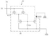
PE 셀들(22)은 데이터 전극라인들(DL)로 공급되는 비디오신호(즉, 전류신호)에 대응되는 빛을 발광함으로써 비디오신호에 대응하는 화상을 표시한다. 이를 위하여, PE 셀들(22) 각각은 도 3과 같이 데이터 전극라인(DL)과 게이트 전극라인들(GL) 각각으로부터 공급되는 구동신호에 따라 발광셀(OLED)을 구동시키 기 위한 발광셀 구동회로(30)와, 발광셀 구동회로(30)와 기저전압원(GND) 사이에 접속되는 발광셀(OLED)을 구비한다.The
발광셀 구동회로(30)는 전압공급라인(VDD)과 발광셀(OLED) 사이에 접속된 제 1구동 박막트랜지스터(Thin Film Transistor : 이하 "TFT"라 함)(T1)와, 게이트 전극라인(GL)과 데이터 전극라인(DL) 사이에 접속된 제 1스위칭 TFT(T3)와, 제 1스위칭 TFT(T3)와 전압공급라인(VDD) 사이에 접속되어 제 1구동 TFT(T1)와 전류미러 회로를 형성하는 제 2구동 TFT(T2)와, 게이트 전극라인(GL)과 제 2구동 TFT(T2) 사이에 접속되는 제 2스위칭 TFT(T4)와, 제 1 및 제 2구동 TFT(T1,T2) 사이의 노드와 전압공급라인(VDD) 사이에 접속된 스토리지 캐패시터(Cst)를 구비한다. 여기서, TFT들은 P 타입 전자 금속 산화막 반도체 전계 효과 트랜지스터(MOSFET, Metal-Oxide Semiconductor Field Effect Transistor)이다.The light emitting
제 1구동 TFT(T1)의 게이트단자는 제 2구동 TFT(T2)의 게이트단자에 접속되고, 소오스단자는 전압공급라인(VDD)에 접속된다. 그리고, 제 1구동 TFT(T1)의 드레인단자는 발광 셀(OLED)에 접속된다. 제 2구동 TFT(T2)의 소오스단자는 전압공급라인(VDD)에 접속되고, 드레인단자는 제 1스위칭 TFT(T3)의 드레인단자와 제 2스위칭 TFT(T4)의 소오스단자에 접속된다.The gate terminal of the first driving TFT T1 is connected to the gate terminal of the second driving TFT T2, and the source terminal is connected to the voltage supply line VDD. The drain terminal of the first driving TFT T1 is connected to the light emitting cell OLED. The source terminal of the second driving TFT T2 is connected to the voltage supply line VDD, and the drain terminal is connected to the drain terminal of the first switching TFT T3 and the source terminal of the second switching TFT T4.
제 1스위칭 TFT(T3)의 소오스단자는 데이터 전극라인(DL)에 접속되고, 게이트단자는 게이트 전극라인(GL)에 접속된다. 제 2스위칭 TFT(T4)의 드레인단자는 제 1 및 제 2구동 TFT(T1,T2)의 게이트단자 및 스토리지 캐패시터(Cst)에 접속된다. 그리고, 제 2스위칭 TFT(T4)의 게이트단자는 게이트 전극라인(GL)에 접속된 다.The source terminal of the first switching TFT T3 is connected to the data electrode line DL, and the gate terminal is connected to the gate electrode line GL. The drain terminal of the second switching TFT T4 is connected to the gate terminals of the first and second driving TFTs T1 and T2 and the storage capacitor Cst. The gate terminal of the second switching TFT T4 is connected to the gate electrode line GL.
여기서, 제 1 및 제 2구동 TFT(T1,T2)는 전류미러를 형성되도록 접속된다. 따라서, 제 1 및 제 2구동 TFT(T1,T2)가 동일한 채널폭을 갖는다고 가정하면 제 1 및 제 2구동 TFT(T1,T2)에 흐르는 전류양은 동일하게 설정된다.Here, the first and second driving TFTs T1 and T2 are connected to form a current mirror. Therefore, assuming that the first and second driving TFTs T1 and T2 have the same channel width, the amount of current flowing through the first and second driving TFTs T1 and T2 is set the same.
이와 같은 발광셀 구동회로(30)의 동작과정을 설명하면, 먼저 수평라인을 이루는 게이트 전극라인(GL)으로부터 게이트신호가 공급된다. 게이트신호가 공급되면 제 1 및 제 2스위칭 TFT(T3,T4)가 턴-온된다. 제 1 및 제 2스위칭 TFT(T3,T4)가 턴-온되면 데이터 전극라인(DL)으로부터의 비디오신호가 제 1 및 제 2스위칭 TFT(T3,T4)를 경유하여 제 1 및 제 2구동 TFT(T1,T2)의 게이트단자로 공급된다. 이때, 비디오신호를 공급받은 제 1 및 제 2구동 TFT(T1,T2)가 턴-온된다. 여기서, 제 1구동 TFT(T1)는 자신의 게이트단자에 공급되는 비디오신호에 따라 자신의 소오스단자(즉, VDD)로부터 드레인단자로 흐르는 전류를 조절하여 발광셀(OLED)로 공급함으로써 발광셀(OLED)에서 비디오신호에 대응되는 밝기의 빛이 발광되도록 제어한다.Referring to the operation of the light emitting
이와 동시에 제 2구동 TFT(T2)는 전압공급라인(VDD)으로부터 공급되는 전류(id)를 제 1스위칭 TFT(T3)를 경유하여 데이터 전극라인(DL)으로 공급한다. 여기서, 제 1 및 제 2구동 TFT(T1,T2)가 전류미러 회로를 형성하기 때문에 제 1 및 제 2구동 TFT(T1,T2)에는 동일한 전류가 흐르게 된다. 한편, 스토리지 캐패시터(Cst)는 제 2구동 TFT(T2)로 흐르는 전류(id)양에 대응되도록 전압공급라인(VDD)으로부터의 전압을 저장한다. 그리고, 스토리지 캐패시터(Cst)는 게이트신 호가 오프로 전환되어 제 1 및 제 2스위칭 TFT(T3,T4)가 턴-오프될 때 자신에게 저장된 전압을 이용하여 제 1구동 TFT(T1)를 턴-온시킴으로써 발광셀(OLED)로 비디오신호에 대응되는 전류가 공급되도록 한다.At the same time, the second driving TFT T2 supplies the current id supplied from the voltage supply line VDD to the data electrode line DL via the first switching TFT T3. Here, since the first and second driving TFTs T1 and T2 form a current mirror circuit, the same current flows through the first and second driving TFTs T1 and T2. Meanwhile, the storage capacitor Cst stores the voltage from the voltage supply line VDD so as to correspond to the amount of current id flowing to the second driving TFT T2. The storage capacitor Cst turns on the first driving TFT T1 using the voltage stored therein when the gate signal is turned off and the first and second switching TFTs T3 and T4 are turned off. By turning on, a current corresponding to the video signal is supplied to the light emitting cell OLED.
여기서, 종래의 데이터 드라이버(20)는 타이밍 콘트롤러(24)로부터 공급되는 데이터에 대응하여 소정의 전류가 PE 셀(22)로부터 공급되도록 제어한다. 즉, 종래의 데이터 드라이버(20)는 전류를 이용하여 PE 셀(22)들을 구동하게 된다.Here, the
이를 위하여, 종래의 데이터 드라이버(20)는 다수의 데이터 드라이브 집적회로(Integraged Circuit : 이하 "IC"라 함)를 구비하며, 상기 다수의 데이터 드라이브 IC 각각은 도 4와 같이 구성된다To this end, the
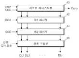
도 4를 참조하면, 데이터 드라이브 IC는 쉬프트 레지스터(40), 제 1래치부(42), 제 2래치부(44) 및 전류 구동부(46)를 구비한다.Referring to FIG. 4, the data drive IC includes a
쉬프트 레지스터부(40)는 타이밍 콘트롤러(24)로부터 공급되는 소스 스타트 펄스(SSP)를 소스 샘플링 클럭(SSC)에 대응하여 순차적으로 쉬프트시켜 샘플링신호를 출력한다.The
제 1래치부(42)는 쉬프트 레지스터부(40)로부터의 샘플링신호에 응답하여 타이밍 콘트롤러(24)로부터 공급되는 데이터(data)를 일정단위씩 순차적으로 샘플링하여 래치하게 된다. 이를 위하여 제 1래치부(42)는 i(i는 자연수)개의 데이터(data)를 래치하기 위한 i개의 래치들로 구성되고, 그 래치들 각각은 데이터(data)의 비트수에 대응하는 크기를 갖는다. 제 1래치부(42)에 저장된 데이터(data)는 제 2래치부(44)로 공급된다.The
제 2래치부(44)는 제 1래치부(42)로부터 공급되는 데이터(data)들을 일시저정함과 아울러 저장된 데이터들(data)을 타이밍 콘트롤러(24)로부터 공급되는 소스 출력 인에이블(SOE) 신호에 응답하여 동시에 출력한다.The
전류 구동부(46)는 제 2래치부(44)로부터 입력되는 데이터에 대응하는 전류가 PE 셀(30)로부터 공급될 수 있도록 제어한다. 이를 도 5를 참조하여 상세히 설명하면, 전류 구동부(46) 각각은 채널마다(즉 i개) 전류구동블록(48)을 구비한다. 전류구동블록(48)은 제 2래치부(44)로부터 데이터를 공급받고, 공급받은 데이터에 대응하는 전류감마신호를 이용하여 PE 셀(30)로부터 데이터에 대응하는 전류(id)가 공급될 수 있도록 제어한다. 따라서, 각각의 데이터라인들(DL)로는 소정의 비디오신호(즉, 전류)에 대응하는 전류(id)가 공급되어 데이터(data)에 대응하는 소정의 화상이 표시되게 된다.The
상술한 바와 같이 종래의 EL 표시장치는 전류만을 이용하여 PE 셀(30)을 구동시킨다. 하지만, 전류만을 이용하여 PE 셀(30)을 구동시키면 발광셀(OLED)에서 원하는 계조의 화상이 표시되지 못하는 문제점이 발생된다. 다시 말하여, 종래의 EL 표시장치는 데이터에 대응하여 ㎂단위로 변하는 전류값을 공급한다. 예를 들어, 데이터 드라이브 IC는 1의 계조에서는 1㎂의 전류가 흐르도록 제어하고, 2의 계조에서는 2㎂의 전류가 흐르도록 제어한다. 하지만, 이와 같이 ㎂단위로 변하는 전류값이 1수평기간(1H)동안 공급되면 스토리지 캐패시터(Cst)에 전류에 대응하는 전압이 충전되지 못한다. 다시 말하여, 스토리지 캐패시터(Cst)는 전류만을 이용하여 PE 셀(30)을 구동하기 때문에 제한된 시간(1H) 안에 전류에 대응하는 전압이 충전되지 못하고, 이에 따라 원하는 계조의 화상이 표시되지 못하는 문제점이 있다.As described above, the conventional EL display device drives the
따라서, 본 발명의 목적은 전압을 이용하여 화소셀들을 프리차징 함으로써 원하는 계조의 화상을 표시할 수 있도록 한 일렉트로-루미네센스 표시장치 및 그 구동방법을 제공하는 것이다.
Accordingly, it is an object of the present invention to provide an electro-luminescence display device and a driving method thereof capable of displaying an image of a desired gray scale by precharging pixel cells using a voltage.
상기 목적을 달성하기 위하여 본 발명의 일렉트로-루미네센스 표시장치는 게이트라인들 및 상기 게이트라인들과 교차되도록 형성된 데이터라인들과, 게이트라인들 및 데이터라인들의 교차부마다 형성되는 화소셀들과, 1수평기간 단위로 게이트신호를 게이트라인들로 순차적으로 공급하기 위한 게이트 드라이버와, 1수평기간 중 제 1기간동안 화소셀들로 전압신호를 공급함과 아울러 제 1수평기간 중 제 1기간을 제외한 제 2기간동안 화소셀들로부터 전류신호를 공급받는 다수의 데이터 집적회로를 구비한다.In order to achieve the above object, an electro-luminescence display device of the present invention includes gate lines and data lines formed to intersect the gate lines, pixel cells formed at intersections of the gate lines and data lines; And a gate driver for sequentially supplying the gate signal to the gate lines in units of one horizontal period, and supplying a voltage signal to the pixel cells during the first period during the first horizontal period, and excluding the first period during the first horizontal period. A plurality of data integrated circuits receive current signals from the pixel cells during the second period.
상기 제 1기간은 상기 제 2기간보다 짧게 설정된다.The first period is set shorter than the second period.
상기 다수의 데이터 집적회로 각각은 자신에게 공급되는 데이터에 대응하는 전압신호를 데이터라인들로 공급하기 위한 전압 구동부와, 데이터에 대응하는 전류신호가 화소셀로부터 공급될 수 있도록 제어하는 전류 구동부를 구비한다.Each of the plurality of data integrated circuits includes a voltage driver for supplying a voltage signal corresponding to data supplied thereto to data lines, and a current driver for controlling a current signal corresponding to data to be supplied from the pixel cell. do.
상기 데이터에 대응하는 전압신호가 생성될 수 있도록 전압 구동부로 다수의 전압레벨을 가지는 감마전압값을 공급하는 감마 전압부를 추가로 구비한다.A gamma voltage unit is further provided to supply a gamma voltage value having a plurality of voltage levels to the voltage driver so that a voltage signal corresponding to the data can be generated.
상기 전압구동부는 데이터 집적회로가 i(i는 자연수)개의 채널을 가질 때 i개 설치되어 데이터에 대응하는 전압신호를 생성하는 전압구동블록과, 전압구동블록 각각과 데이터라인 사이에 설치되어 외부로부터 공급되는 제어신호의 제 1극성에 의하여 턴-온되는 제 1스위칭부를 구비한다.The voltage driving unit includes a voltage driving block which is installed when the data integrated circuit has i (i is a natural number) channels and generates a voltage signal corresponding to the data, and is installed between each of the voltage driving blocks and the data line. And a first switching unit turned on by the first polarity of the supplied control signal.
상기 전류구동부는 i개 설치되어 데이터에 대응하여 전류신호가 공급되도록 제어하는 전류구동블록과, 전류구동블록 각각과 데이터라인 사이에 설치되어 제어신호의 제 2극성에 의하여 턴-온되는 제 2스위칭부를 구비한다.The current driving unit is provided with i current control block for controlling the current signal is supplied in response to the data, and the second switching is provided between each of the current driving block and the data line is turned on by the second polarity of the control signal A part is provided.
상기 제어신호는 제 1기간동안 제 1극성을 유지하고, 제 2기간동안 제 2극성을 유지한다.The control signal maintains a first polarity for a first period and a second polarity for a second period.
상기 전압신호는 화소셀에 포함된 스토리지 캐패시터에 충전된다.The voltage signal is charged in a storage capacitor included in the pixel cell.
본 발명의 일렉트로-루미네센스 표시장치의 구동방법은 게이트신호를 공급하여 특정 수평라인에 설치된 화소셀들을 선택하는 단계와, 화소셀들에 제 1기간동안 데이터에 대응하는 전압값을 공급하여 화소셀들을 프리차징하는 단계와, 제 1기간이후의 제 2기간동안 화소셀들로부터 데이터에 대응하는 전류값이 흐르도록 제어하여 데이터에 대응하는 화상을 표시하는 단계를 포함한다.A method of driving an electro-luminescence display device according to the present invention includes supplying a gate signal to select pixel cells installed on a specific horizontal line, and supplying a voltage value corresponding to data for a first period of time to the pixel cells. Precharging the cells, and controlling a current value corresponding to the data to flow from the pixel cells during the second period after the first period to display an image corresponding to the data.
상기 제 1기간 및 제 2기간은 1수평기간마다 반복된다.The first period and the second period are repeated every one horizontal period.
상기 제 1기간은 제 2기간보다 짧게 설정된다.The first period is set shorter than the second period.
본 발명의 일렉트로-루미네센스 표시장치의 구동방법은 게이트 드라이버에서 1수평기간 단위로 게이트신호를 공급하여 특정 수평라인에 설치된 화소셀들을 선택하는 단계와, 1수평기간 중 제 1기간동안 전압 구동부에서 데이터에 대응하는 전압값을 화소셀들로 공급하는 단계와, 1수평기간 중 제 1기간을 제외한 제 2기간동안 전류 구동부에서 데이터에 대응하는 전류가 화소셀들로부터 자신에게 공급될 수 있도록 제어하는 단계를 포함한다.A method of driving an electro-luminescence display device according to the present invention includes supplying a gate signal in units of one horizontal period from a gate driver to select pixel cells installed in a specific horizontal line, and a voltage driver for a first period of one horizontal period. Supplying a voltage value corresponding to the data to the pixel cells in the control panel, and controlling a current corresponding to the data to be supplied from the pixel cells to the current driver during the second period except for the first period of one horizontal period. It includes a step.
상기 전압값을 상기 화소셀들로 공급하는 단계는 데이터에 대응하여 다수의 전압값들 중 어느 하나의 전압값을 선택하여 화소셀들로 공급한다.The step of supplying the voltage value to the pixel cells selects one of a plurality of voltage values corresponding to the data and supplies the selected voltage value to the pixel cells.
상기 제 1기간은 제 2기간보다 짧게 설정된다.The first period is set shorter than the second period.
상기 목적 외에 본 발명의 다른 목적 및 특징들은 첨부도면을 참조한 실시예에 대한 설명을 통하여 명백하게 드러나게 될 것이다.Other objects and features of the present invention in addition to the above objects will become apparent from the description of the embodiments with reference to the accompanying drawings.
이하 도 6 내지 도 9를 참조하여 본 발명의 바람직한 실시예에 대하여 설명하기로 한다.Hereinafter, exemplary embodiments of the present invention will be described with reference to FIGS. 6 to 9.
도 6은 EL 표시장치의 데이터 드라이버에 다수 포함되는 데이터 드라이브 집적회로를 나타내는 도면이다.Fig. 6 is a diagram showing a data drive integrated circuit included in a large number of data drivers of an EL display device.
도 6을 참조하면, 본 발명의 실시예에 의한 데이터 드라이브 IC는 쉬프트 레지스터부(50), 제 1래치부(52), 제 2래치부(54) 및 구동부(56)를 구비한다.Referring to FIG. 6, a data drive IC according to an exemplary embodiment of the present invention includes a
쉬프트 레지스터부(50)는 도시되지 않는 타이밍 콘트롤러로부터 소스 스타트 펄스(SSP)를 소스 샘플링 클럭(SSC)에 대응하여 순차적으로 쉬프트시켜 샘플링신호를 출력한다. 여기서, 쉬프트 레지스터부(50)는 데이터 드라이브 IC가 i(i는 자연수)개의 채널을 갖는 경우 i개의 샘플링신호를 출력하기 위하여 i개의 쉬프트 레지 스터를 구비한다.The
제 1래치부(52)는 쉬프트 레지스터부(50)로부터의 샘플링신호에 응답하여 타이밍 콘트롤러로부터 공급되는 데이터(data)를 일정단위씩 순차적으로 샘플링하여 래치한다. 이를 위하여, 제 1래치부(52)는 i개의 데이터(data)를 래치하기 위한 i개의 래치들로 구성되고, 그 래치들 각각은 데이터(data)의 비트수에 대응하는 크기를 갖는다. 제 1래치부(52)에 저장된 데이터들(data)은 제 2래치부(54)로 공급된다.The
제 2래치부(54)는 제 1래치부(52)로부터 공급되는 데이터들(data)들을 일시 저장함과 아울러 저장된 데이터들(data)을 타이밍 콘트롤러로부터 공급되는 소스 출력 인에이블(SOE) 신호에 응답하여 동시에 출력한다.The
구동부(56)는 타이밍 콘트롤러로부터 공급되는 제어신호(CS)에 응답하여 전류신호(비디오신호) 및 전압신호 중 어느 하나의 신호를 데이터라인들(DL)로 공급한다. 여기서, 데이터라인들(DL)로 전류신호가 공급될 때 실제로 전류는 PE 셀로부터 구동부(56) 쪽으로 흐르게 된다. 그리고, 데이터라인들(DL)로 공급되는 전압신호는 PE 셀로 공급되어 PE 셀을 프리차징시킨다.The driver 56 supplies one of a current signal (video signal) and a voltage signal to the data lines DL in response to the control signal CS supplied from the timing controller. Here, when the current signal is supplied to the data lines DL, the current actually flows from the PE cell toward the driver 56. The voltage signals supplied to the data lines DL are supplied to the PE cells to precharge the PE cells.
이를 위하여, 구동부(56)는 전류 구동부(58) 및 전압 구동부(60)를 구비한다. 전류 구동부(58)는 데이터에 대응하는 전류가 PE 셀로부터 자신쪽으로 공급되도록 제어함으로써 PE 셀에서 데이터에 대응하는 화상이 표시되도록 한다. 전압 구동부(60)는 데이터에 대응하는 전압을 PE 셀로 공급하여 PE 셀에 데이터에 대응하는 전압값이 프리차징되도록 한다.To this end, the driver 56 includes a
이를 위하여, 전압 구동부(60)는 도시되지 않은 감마전압부로부터 전압감마신호를 공급받는다. 실제로, 감마전압부는 데이터에 대응되도록 서로 상이한 전압값을 가지는 다수의 전압감마신호를 전압 구동부(60)로 공급하고, 전압 구동부(60)는 다수의 전압감마신호 중 데이터에 대응하는 전압감마신호를 데이터라인들(DL)로 공급한다.To this end, the
한편, 전류 구동부(58) 각각은 도 7과 같이 채널수와 동일한 i개의 전류구동블록(62) 및 제 1스위칭부(64)을 구비한다. i개의 전류구동블록(62)은 제 1스위칭부(64)를 경유하여 i개의 데이터라인들(DL)과 각각 접속된다. 그리고, 전압 구동부(60) 각각은 도 7과 같이 채널수와 동일한 i개의 전압구동블록(66) 및 제 2스위칭부(68)을 구비한다. i개의 전압구동블록(66)은 제 2스위칭부(68)를 경유하여 i개의 데이터라인들(DL)과 각각 접속된다.Meanwhile, each of the
전류구동블록(62)은 제 2래치부(54)로부터 공급되는 데이터에 대응되도록 전류감마신호를 선택하고, 선택된 전류감마신호를 이용하여 PE 셀로부터 데이터에 대응하는 전류가 공급될 수 있도록 제어한다. 전압구동블록(66)은 제 2래치부(54)로부터 공급되는 데이터에 대응되도록 감마전압부로부터 공급되는 다수의 전압감마신호 중 어느 하나를 선택하고, 선택된 전압감마신호를 데이터라인(DL)으로 공급함으로써 PE 셀이 프라치징될 수 있도록 제어한다.The
제 1스위칭부(64)는 자신에게 공급되는 제어신호(CS)의 제 1극성(예를 들면, 로우)에 대응하여 데이터라인(DL)과 전류구동블록(62)을 전기적으로 접속시킨다. 이때, 데이터라인(DL)에는 전류구동블록(62)의 제어에 의하여 소정의 전류값이 흐 르게 된다. 제 2스위칭부(68)는 자신에게 공급되는 제어신호(CS)의 제 2극성(예를 들면, 하이)에 대응하여 데이터라인(DL)과 전압구동블록(66)을 전기적으로 접속시킨다. 이때, 데이터라인(DL)에는 전압구동블록(66)의 제어에 의하여 소정의 전압값이 공급된다.The
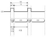
한편, 제어신호(CS)는 도 8에 도시된 바와 같이 1수평기간(1H)의 주기를 갖고 하이 및 로우를 반복한다. 여기서, 제어신호(CS)가 제 2극성(하이)을 갖는 제 1시간(T1) 동안 제 2스위칭부(68)가 턴-온되어 데이터라인들(DL)에는 데이터에 대응하는 전압감마신호가 공급된다. 이때, PE 셀들은 데이터에 대응하는 전압감마신호(즉, 전압값)를 프리차징(VD:전압)하게 된다. 그리고, 제어신호(CS)가 제 1극성(로우)을 갖는 제 2시간(T2) 동안 제 1스위칭부(64)가 턴-온되어 데이터라인들(DL)에는 데이터에 대응하는 전류값이 흐르게 된다. 이때, PE 셀들에는 데이터에 대응하는 전압값이 차징(CD:전류)됨과 아울러 데이터에 대응하는 화상이 표시된다.Meanwhile, the control signal CS repeats high and low with a period of one
한편, 제 1시간(T1)은 제 2시간(T2)보다 짧게 설정된다. 다시 말하여, 본 발명에서는 1수평기간(1H) 중 짧게 설정된 제 1시간(T1) 동안에는 전압값을 PE 셀에 프리차징함과 아울러 1수평기간(1H) 중 길게 설정된 제 2시간(T2) 동안에는 전류가 공급되도록 함으로써 PE 셀에 원하는 전압을 차징함과 아울러 데이터에 대응하는 화상을 표시할 수 있다.On the other hand, the first time T1 is set shorter than the second time T2. In other words, in the present invention, the voltage value is precharged in the PE cell during the first time T1 set shortly in one
이와 같은 본 발명의 EL 표시장치의 상세한 동작과정을 도 9를 참조하여 상세히 설명하기로 한다.Such a detailed operation process of the EL display device of the present invention will be described in detail with reference to FIG.
먼저, 게이트 드라이버(72)로부터 게이트신호가 공급되어 특정 수평라인에 형성된 PE 셀(70)이 선택된다.(여기서 PE 셀(70)의 상세한 구성은 도 3과 동일하므로 상세한 설명은 생략하기로 한다) 여기서, 게이트신호가 공급되면 제 1 및 제 2스위칭 TFT(T3,T4)가 턴-온된다.First, a gate signal is supplied from the
이때, 도 8에 도시된 바와 같이 1수평기간(1H)의 초반부 제 1시간(T1) 동안에는 제 2스위칭부(68)가 턴-온된다. 따라서, 전압구동블록(66)으로부터 데이터에 대응하는 전압감마신호가 데이터라인(DL)으로 공급된다. 이때, 제 1 및 제 2스위칭 TFT(T3,T4)가 턴-온되었기 때문에 전압감마신호는 제 1 및 제 2스위칭 TFT(T3,T4)를 경유하여 스토리지 캐패시터(Cst)에 충전되게 된다. 즉, 본 발명에서는 제 1시간(T1) 동안 스토리지 캐패시터(Cst)에 데이터에 대응하는 전압값을 충전(프리차징)하게 된다.In this case, as illustrated in FIG. 8, the
이후, 제 2시간(T2) 동안 제 2스위칭부(68)가 턴-오프됨과 아울러 제 1스위칭부(64)가 턴-온된다.(즉, 제 1 및 제 2스위칭부(64,68)는 교번적으로 턴-온된다) 제 1스위칭부(64)가 턴-온되면 전류구동블록(62)이 제 1스위칭부(64), 데이터라인(DL) 및 제 1 및 제 2스위칭 TFT(T3,T4)를 경유하여 제 1 및 제 2구동 TFT(T1,T2)의 게이트단자와 전기적으로 접속된다. 이때, 제 1 및 제 2구동 TFT(T1,T2)가 턴-온된다. 제 2구동 TFT(T2)가 턴-온되면 전압공급라인(VDD)으로부터 공급되는 전류가 제 1스위칭 TFT(T3)를 경유하여 전류구동블록(62)으로 공급된다. 여기서, 제 1스위칭 TFT(T3)를 경유하여 흐르는 전류는 전류구동블록(62)에 입력되는 데이터에 대응하여 선택된 전류감마신호에 의하여 결정된다.Thereafter, the
한편, 제 1 및 제 2구동 TFT(T1,T2)가 전류미러 회로를 형성하기 때문에 제 1구동 TFT(T1)에도 동일한 전류가 흐르게 된다. 따라서, 발광셀(OLED)은 제 1구동 TFT(T1)로부터 공급되는 전류에 대응되는 밝기의 빛을 발광함으로써 소정의 화상이 패널(74) 상에 표시되도록 한다. 그리고, 스토리지 캐패시터(Cst)는 제 2구동 TFT(T2)로 흐르는 전류양에 대응되도록 소정의 전압이 저장된다. 여기서, 스토리지 캐피시터(Cst)는 제 1시간(T1) 동안 데이터의 전압이 프리차징되었기 때문에 전류양에 대응되는 충분한 전압이 충전된다. 그리고, 스토리지 캐패시터(Cst)는 게이트신호가 오프로 전환되어 제 1 및 제 2스위칭 TFT(T3,T4)가 턴-오프될 때 자신에게 저장된 전압을 이용하여 제 1구동 TFT(T1)를 턴-온시킴으로써 발광셀(OLED)로 비디오신호에 대응되는 전류가 공급되도록 한다.On the other hand, since the first and second driving TFTs T1 and T2 form a current mirror circuit, the same current also flows through the first driving TFT T1. Therefore, the light emitting cell OLED emits light of brightness corresponding to the current supplied from the first driving TFT T1 so that a predetermined image is displayed on the
즉, 본 발명에서는 1수평기간(1H) 중 일부기간인 프리차징기간동안 전압값을 이용하여 PE 셀(70)을 충전함으로써 PE 셀(70)에 데이터에 대응하는 전압값이 충전되도록 한다. 이후, 1수평기간(1H) 중 나머지 기간동안 데이터에 대응하는 전류값이 PE 셀(70)에서 흐르도록 제어함으로써 PE 셀(70)에 데이터에 대응하는 정확한 전압값이 충분히 충전되도록 한다. 따라서, 본 발명에서는 발광셀(OLED)에서 원하는 계조의 화상이 표시될 수 있고, 이에 따라 화질을 향상시킬 수 있다.That is, in the present invention, the
상술한 바와 같이, 본 발명에 따른 일렉트로-루미네센스 표시장치 및 그 구동방법에 의하면 게이트신호가 공급되는 1수평기간 중 일부기간동안 화소셀들로 전 압값을 공급하여 화소셀들을 프리차징한다. 그리고, 1수평기간 중 나머지 기간동안 화소셀로부터 데이터에 대응하는 전류값이 흐를 수 있도록 제어하고, 이에 따라 화소셀들에 데이터에 대응하는 정확한 전압값이 차징되게 된다. 즉, 본 발명에서는 전압값을 이용하여 화소셀들을 프리차징함으로써 화소셀들에서 데이터에 대응하는 계조값을 가지는 빛이 생성될 수 있고, 이에 따라 화질을 향상시킬 수 있다.As described above, according to the electro-luminescence display device and the driving method thereof according to the present invention, the pixel cells are precharged by supplying voltage values to the pixel cells during a part of one horizontal period during which the gate signal is supplied. Then, the current value corresponding to the data flows from the pixel cell for the remainder of the one horizontal period, so that the correct voltage value corresponding to the data is charged to the pixel cells. That is, in the present invention, light having a gray scale value corresponding to data may be generated in the pixel cells by precharging the pixel cells using the voltage value, thereby improving image quality.
이상 설명한 내용을 통해 당업자라면 본 발명의 기술사상을 일탈하지 아니하는 범위에서 다양한 변경 및 수정이 가능함을 알 수 있을 것이다. 따라서, 본 발명의 기술적 범위는 명세서의 상세한 설명에 기재된 내용으로 한정되는 것이 아니라 특허 청구의 범위에 의해 정하여져야만 할 것이다.Those skilled in the art will appreciate that various changes and modifications can be made without departing from the technical spirit of the present invention. Therefore, the technical scope of the present invention should not be limited to the contents described in the detailed description of the specification but should be defined by the claims.
Claims (14)
Translated fromKoreanPriority Applications (5)
| Application Number | Priority Date | Filing Date | Title |
|---|---|---|---|
| KR1020030099806AKR100580554B1 (en) | 2003-12-30 | 2003-12-30 | Electro-luminescence display and its driving method |
| US10/825,365US7924245B2 (en) | 2003-12-30 | 2004-04-16 | Electro-luminescence display device with data driver capable of applying current and voltage signals and driving method thereof |
| TW093114777ATWI284299B (en) | 2003-12-30 | 2004-05-25 | Electro-luminescence display device and driving method thereof |
| CNB2004100455499ACN100487774C (en) | 2003-12-30 | 2004-05-28 | Electro-luminescence display device and driving method thereof |
| JP2004192096AJP2005196116A (en) | 2003-12-30 | 2004-06-29 | Electroluminescence display device and driving method thereof |
Applications Claiming Priority (1)
| Application Number | Priority Date | Filing Date | Title |
|---|---|---|---|
| KR1020030099806AKR100580554B1 (en) | 2003-12-30 | 2003-12-30 | Electro-luminescence display and its driving method |
Publications (2)
| Publication Number | Publication Date |
|---|---|
| KR20050068417A KR20050068417A (en) | 2005-07-05 |
| KR100580554B1true KR100580554B1 (en) | 2006-05-16 |
Family
ID=34698720
Family Applications (1)
| Application Number | Title | Priority Date | Filing Date |
|---|---|---|---|
| KR1020030099806AExpired - LifetimeKR100580554B1 (en) | 2003-12-30 | 2003-12-30 | Electro-luminescence display and its driving method |
Country Status (5)
| Country | Link |
|---|---|
| US (1) | US7924245B2 (en) |
| JP (1) | JP2005196116A (en) |
| KR (1) | KR100580554B1 (en) |
| CN (1) | CN100487774C (en) |
| TW (1) | TWI284299B (en) |
Cited By (1)
| Publication number | Priority date | Publication date | Assignee | Title |
|---|---|---|---|---|
| KR100939211B1 (en) | 2008-02-22 | 2010-01-28 | 엘지디스플레이 주식회사 | Organic light emitting diode display and its driving method |
Families Citing this family (91)
| Publication number | Priority date | Publication date | Assignee | Title |
|---|---|---|---|---|
| US7569849B2 (en) | 2001-02-16 | 2009-08-04 | Ignis Innovation Inc. | Pixel driver circuit and pixel circuit having the pixel driver circuit |
| JP2003177709A (en)* | 2001-12-13 | 2003-06-27 | Seiko Epson Corp | Pixel circuit for light emitting element |
| CA2419704A1 (en) | 2003-02-24 | 2004-08-24 | Ignis Innovation Inc. | Method of manufacturing a pixel with organic light-emitting diode |
| CA2443206A1 (en) | 2003-09-23 | 2005-03-23 | Ignis Innovation Inc. | Amoled display backplanes - pixel driver circuits, array architecture, and external compensation |
| JP4016968B2 (en)* | 2004-05-24 | 2007-12-05 | セイコーエプソン株式会社 | DA converter, data line driving circuit, electro-optical device, driving method thereof, and electronic apparatus |
| CA2472671A1 (en)* | 2004-06-29 | 2005-12-29 | Ignis Innovation Inc. | Voltage-programming scheme for current-driven amoled displays |
| CA2490858A1 (en) | 2004-12-07 | 2006-06-07 | Ignis Innovation Inc. | Driving method for compensated voltage-programming of amoled displays |
| TWI402790B (en) | 2004-12-15 | 2013-07-21 | Ignis Innovation Inc | Method and system for programming, calibrating and driving a light-emitting element display |
| US8576217B2 (en) | 2011-05-20 | 2013-11-05 | Ignis Innovation Inc. | System and methods for extraction of threshold and mobility parameters in AMOLED displays |
| US9280933B2 (en) | 2004-12-15 | 2016-03-08 | Ignis Innovation Inc. | System and methods for extraction of threshold and mobility parameters in AMOLED displays |
| US9171500B2 (en) | 2011-05-20 | 2015-10-27 | Ignis Innovation Inc. | System and methods for extraction of parasitic parameters in AMOLED displays |
| US10012678B2 (en) | 2004-12-15 | 2018-07-03 | Ignis Innovation Inc. | Method and system for programming, calibrating and/or compensating, and driving an LED display |
| US10013907B2 (en) | 2004-12-15 | 2018-07-03 | Ignis Innovation Inc. | Method and system for programming, calibrating and/or compensating, and driving an LED display |
| US20140111567A1 (en) | 2005-04-12 | 2014-04-24 | Ignis Innovation Inc. | System and method for compensation of non-uniformities in light emitting device displays |
| US9799246B2 (en) | 2011-05-20 | 2017-10-24 | Ignis Innovation Inc. | System and methods for extraction of threshold and mobility parameters in AMOLED displays |
| US9275579B2 (en) | 2004-12-15 | 2016-03-01 | Ignis Innovation Inc. | System and methods for extraction of threshold and mobility parameters in AMOLED displays |
| US8599191B2 (en) | 2011-05-20 | 2013-12-03 | Ignis Innovation Inc. | System and methods for extraction of threshold and mobility parameters in AMOLED displays |
| CA2495726A1 (en) | 2005-01-28 | 2006-07-28 | Ignis Innovation Inc. | Locally referenced voltage programmed pixel for amoled displays |
| CA2496642A1 (en) | 2005-02-10 | 2006-08-10 | Ignis Innovation Inc. | Fast settling time driving method for organic light-emitting diode (oled) displays based on current programming |
| KR100707623B1 (en)* | 2005-03-19 | 2007-04-13 | 한양대학교 산학협력단 | Pixel and light emitting display device using same |
| JP5355080B2 (en) | 2005-06-08 | 2013-11-27 | イグニス・イノベイション・インコーポレーテッド | Method and system for driving a light emitting device display |
| CA2518276A1 (en) | 2005-09-13 | 2007-03-13 | Ignis Innovation Inc. | Compensation technique for luminance degradation in electro-luminance devices |
| TW200746022A (en) | 2006-04-19 | 2007-12-16 | Ignis Innovation Inc | Stable driving scheme for active matrix displays |
| KR100819946B1 (en)* | 2006-07-06 | 2008-04-10 | 엘지.필립스 엘시디 주식회사 | EL display device and driving method thereof |
| CA2556961A1 (en) | 2006-08-15 | 2008-02-15 | Ignis Innovation Inc. | Oled compensation technique based on oled capacitance |
| US9384698B2 (en) | 2009-11-30 | 2016-07-05 | Ignis Innovation Inc. | System and methods for aging compensation in AMOLED displays |
| CA2688870A1 (en) | 2009-11-30 | 2011-05-30 | Ignis Innovation Inc. | Methode and techniques for improving display uniformity |
| US10319307B2 (en) | 2009-06-16 | 2019-06-11 | Ignis Innovation Inc. | Display system with compensation techniques and/or shared level resources |
| US9311859B2 (en) | 2009-11-30 | 2016-04-12 | Ignis Innovation Inc. | Resetting cycle for aging compensation in AMOLED displays |
| CA2669367A1 (en) | 2009-06-16 | 2010-12-16 | Ignis Innovation Inc | Compensation technique for color shift in displays |
| US8497828B2 (en) | 2009-11-12 | 2013-07-30 | Ignis Innovation Inc. | Sharing switch TFTS in pixel circuits |
| US10996258B2 (en) | 2009-11-30 | 2021-05-04 | Ignis Innovation Inc. | Defect detection and correction of pixel circuits for AMOLED displays |
| US8803417B2 (en) | 2009-12-01 | 2014-08-12 | Ignis Innovation Inc. | High resolution pixel architecture |
| CA2687631A1 (en) | 2009-12-06 | 2011-06-06 | Ignis Innovation Inc | Low power driving scheme for display applications |
| TWI427607B (en)* | 2009-12-30 | 2014-02-21 | Hannstar Display Corp | Field sequential liquid crystal display and driving method thereof |
| US10163401B2 (en) | 2010-02-04 | 2018-12-25 | Ignis Innovation Inc. | System and methods for extracting correlation curves for an organic light emitting device |
| US10089921B2 (en) | 2010-02-04 | 2018-10-02 | Ignis Innovation Inc. | System and methods for extracting correlation curves for an organic light emitting device |
| US9881532B2 (en) | 2010-02-04 | 2018-01-30 | Ignis Innovation Inc. | System and method for extracting correlation curves for an organic light emitting device |
| US20140313111A1 (en) | 2010-02-04 | 2014-10-23 | Ignis Innovation Inc. | System and methods for extracting correlation curves for an organic light emitting device |
| CA2692097A1 (en) | 2010-02-04 | 2011-08-04 | Ignis Innovation Inc. | Extracting correlation curves for light emitting device |
| US10176736B2 (en) | 2010-02-04 | 2019-01-08 | Ignis Innovation Inc. | System and methods for extracting correlation curves for an organic light emitting device |
| CA2696778A1 (en) | 2010-03-17 | 2011-09-17 | Ignis Innovation Inc. | Lifetime, uniformity, parameter extraction methods |
| CN102298893B (en)* | 2010-06-28 | 2014-09-17 | 京东方科技集团股份有限公司 | Source electrode driving circuit and display device |
| CN102063885B (en)* | 2010-07-20 | 2016-03-02 | 矽创电子股份有限公司 | Display panel drive circuit |
| US8907991B2 (en) | 2010-12-02 | 2014-12-09 | Ignis Innovation Inc. | System and methods for thermal compensation in AMOLED displays |
| CN109272933A (en) | 2011-05-17 | 2019-01-25 | 伊格尼斯创新公司 | The method for operating display |
| US9606607B2 (en) | 2011-05-17 | 2017-03-28 | Ignis Innovation Inc. | Systems and methods for display systems with dynamic power control |
| US9530349B2 (en) | 2011-05-20 | 2016-12-27 | Ignis Innovations Inc. | Charged-based compensation and parameter extraction in AMOLED displays |
| US9466240B2 (en) | 2011-05-26 | 2016-10-11 | Ignis Innovation Inc. | Adaptive feedback system for compensating for aging pixel areas with enhanced estimation speed |
| US9773439B2 (en) | 2011-05-27 | 2017-09-26 | Ignis Innovation Inc. | Systems and methods for aging compensation in AMOLED displays |
| CN102646388B (en)* | 2011-06-02 | 2015-01-14 | 京东方科技集团股份有限公司 | Driving device, organic light emitting diode (OLED) panel and OLED panel driving method |
| US9070775B2 (en) | 2011-08-03 | 2015-06-30 | Ignis Innovations Inc. | Thin film transistor |
| US8901579B2 (en) | 2011-08-03 | 2014-12-02 | Ignis Innovation Inc. | Organic light emitting diode and method of manufacturing |
| US9385169B2 (en) | 2011-11-29 | 2016-07-05 | Ignis Innovation Inc. | Multi-functional active matrix organic light-emitting diode display |
| US10089924B2 (en) | 2011-11-29 | 2018-10-02 | Ignis Innovation Inc. | Structural and low-frequency non-uniformity compensation |
| US9324268B2 (en) | 2013-03-15 | 2016-04-26 | Ignis Innovation Inc. | Amoled displays with multiple readout circuits |
| US8937632B2 (en) | 2012-02-03 | 2015-01-20 | Ignis Innovation Inc. | Driving system for active-matrix displays |
| KR101960372B1 (en)* | 2012-03-09 | 2019-03-21 | 엘지디스플레이 주식회사 | Organic light emitting diode display device and driving method the same |
| US9747834B2 (en) | 2012-05-11 | 2017-08-29 | Ignis Innovation Inc. | Pixel circuits including feedback capacitors and reset capacitors, and display systems therefore |
| US8922544B2 (en) | 2012-05-23 | 2014-12-30 | Ignis Innovation Inc. | Display systems with compensation for line propagation delay |
| TWI601113B (en)* | 2012-11-26 | 2017-10-01 | 校際微電子中心 | Low power digital driving of active matrix displays |
| US9336717B2 (en) | 2012-12-11 | 2016-05-10 | Ignis Innovation Inc. | Pixel circuits for AMOLED displays |
| US9786223B2 (en) | 2012-12-11 | 2017-10-10 | Ignis Innovation Inc. | Pixel circuits for AMOLED displays |
| US9830857B2 (en) | 2013-01-14 | 2017-11-28 | Ignis Innovation Inc. | Cleaning common unwanted signals from pixel measurements in emissive displays |
| CN108665836B (en) | 2013-01-14 | 2021-09-03 | 伊格尼斯创新公司 | Method and system for compensating for deviations of a measured device current from a reference current |
| US9721505B2 (en) | 2013-03-08 | 2017-08-01 | Ignis Innovation Inc. | Pixel circuits for AMOLED displays |
| EP3043338A1 (en) | 2013-03-14 | 2016-07-13 | Ignis Innovation Inc. | Re-interpolation with edge detection for extracting an aging pattern for amoled displays |
| US9952698B2 (en) | 2013-03-15 | 2018-04-24 | Ignis Innovation Inc. | Dynamic adjustment of touch resolutions on an AMOLED display |
| WO2014174427A1 (en) | 2013-04-22 | 2014-10-30 | Ignis Innovation Inc. | Inspection system for oled display panels |
| CN105474296B (en) | 2013-08-12 | 2017-08-18 | 伊格尼斯创新公司 | A method and device for driving a display using image data |
| US9761170B2 (en) | 2013-12-06 | 2017-09-12 | Ignis Innovation Inc. | Correction for localized phenomena in an image array |
| US9741282B2 (en) | 2013-12-06 | 2017-08-22 | Ignis Innovation Inc. | OLED display system and method |
| US9502653B2 (en) | 2013-12-25 | 2016-11-22 | Ignis Innovation Inc. | Electrode contacts |
| US10997901B2 (en) | 2014-02-28 | 2021-05-04 | Ignis Innovation Inc. | Display system |
| US10176752B2 (en) | 2014-03-24 | 2019-01-08 | Ignis Innovation Inc. | Integrated gate driver |
| DE102015206281A1 (en) | 2014-04-08 | 2015-10-08 | Ignis Innovation Inc. | Display system with shared level resources for portable devices |
| KR102269785B1 (en)* | 2014-06-17 | 2021-06-29 | 삼성디스플레이 주식회사 | Pixel circuit and organic light emitting display device having the same |
| CA2872563A1 (en) | 2014-11-28 | 2016-05-28 | Ignis Innovation Inc. | High pixel density array architecture |
| CA2879462A1 (en) | 2015-01-23 | 2016-07-23 | Ignis Innovation Inc. | Compensation for color variation in emissive devices |
| CA2889870A1 (en) | 2015-05-04 | 2016-11-04 | Ignis Innovation Inc. | Optical feedback system |
| CA2892714A1 (en) | 2015-05-27 | 2016-11-27 | Ignis Innovation Inc | Memory bandwidth reduction in compensation system |
| US10657895B2 (en) | 2015-07-24 | 2020-05-19 | Ignis Innovation Inc. | Pixels and reference circuits and timing techniques |
| CA2898282A1 (en) | 2015-07-24 | 2017-01-24 | Ignis Innovation Inc. | Hybrid calibration of current sources for current biased voltage progra mmed (cbvp) displays |
| US10373554B2 (en) | 2015-07-24 | 2019-08-06 | Ignis Innovation Inc. | Pixels and reference circuits and timing techniques |
| CA2900170A1 (en) | 2015-08-07 | 2017-02-07 | Gholamreza Chaji | Calibration of pixel based on improved reference values |
| CA2909813A1 (en) | 2015-10-26 | 2017-04-26 | Ignis Innovation Inc | High ppi pattern orientation |
| US10586491B2 (en) | 2016-12-06 | 2020-03-10 | Ignis Innovation Inc. | Pixel circuits for mitigation of hysteresis |
| US10714018B2 (en) | 2017-05-17 | 2020-07-14 | Ignis Innovation Inc. | System and method for loading image correction data for displays |
| US11025899B2 (en) | 2017-08-11 | 2021-06-01 | Ignis Innovation Inc. | Optical correction systems and methods for correcting non-uniformity of emissive display devices |
| US10971078B2 (en) | 2018-02-12 | 2021-04-06 | Ignis Innovation Inc. | Pixel measurement through data line |
| CN111883065B (en)* | 2020-08-17 | 2022-02-15 | 京东方科技集团股份有限公司 | Pixel circuit and driving method thereof, and display substrate |
Family Cites Families (26)
| Publication number | Priority date | Publication date | Assignee | Title |
|---|---|---|---|---|
| JP4081852B2 (en)* | 1998-04-30 | 2008-04-30 | ソニー株式会社 | Matrix driving method for organic EL element and matrix driving apparatus for organic EL element |
| JP2000356972A (en)* | 1999-06-15 | 2000-12-26 | Pioneer Electronic Corp | Device and method for driving light emitting panel |
| JP2001042827A (en)* | 1999-08-03 | 2001-02-16 | Pioneer Electronic Corp | Display device and driving circuit of display panel |
| JP4491632B2 (en)* | 2000-04-07 | 2010-06-30 | 日本電気株式会社 | Driving method of liquid crystal display device |
| US6583576B2 (en)* | 2000-05-08 | 2003-06-24 | Semiconductor Energy Laboratory Co., Ltd. | Light-emitting device, and electric device using the same |
| JP2003195815A (en)* | 2000-11-07 | 2003-07-09 | Sony Corp | Active matrix type display device and active matrix type organic electroluminescence display device |
| JP3685712B2 (en)* | 2000-11-16 | 2005-08-24 | シャープ株式会社 | Dynamic gamma correction device |
| TWI248319B (en)* | 2001-02-08 | 2006-01-21 | Semiconductor Energy Lab | Light emitting device and electronic equipment using the same |
| JP3570394B2 (en)* | 2001-05-25 | 2004-09-29 | ソニー株式会社 | Active matrix type display device, active matrix type organic electroluminescence display device, and driving method thereof |
| KR100777702B1 (en)* | 2001-06-04 | 2007-11-21 | 삼성전자주식회사 | Flat panel display device and driving method thereof |
| US6956547B2 (en)* | 2001-06-30 | 2005-10-18 | Lg.Philips Lcd Co., Ltd. | Driving circuit and method of driving an organic electroluminescence device |
| JP3951687B2 (en) | 2001-08-02 | 2007-08-01 | セイコーエプソン株式会社 | Driving data lines used to control unit circuits |
| KR100819138B1 (en)* | 2001-08-25 | 2008-04-21 | 엘지.필립스 엘시디 주식회사 | Driving device of electroluminescence panel and driving method thereof |
| JP5636147B2 (en) | 2001-08-28 | 2014-12-03 | パナソニック株式会社 | Active matrix display device |
| WO2003023752A1 (en) | 2001-09-07 | 2003-03-20 | Matsushita Electric Industrial Co., Ltd. | El display, el display driving circuit and image display |
| JP2003108065A (en) | 2001-09-28 | 2003-04-11 | Matsushita Electric Ind Co Ltd | Active matrix display device and driving method thereof |
| WO2003034384A2 (en)* | 2001-10-19 | 2003-04-24 | Clare Micronix Integrated Systems, Inc. | Method and system for precharging oled/pled displays with a precharge latency |
| JP2003177709A (en)* | 2001-12-13 | 2003-06-27 | Seiko Epson Corp | Pixel circuit for light emitting element |
| JP3807322B2 (en)* | 2002-02-08 | 2006-08-09 | セイコーエプソン株式会社 | Reference voltage generation circuit, display drive circuit, display device, and reference voltage generation method |
| JP3866606B2 (en)* | 2002-04-08 | 2007-01-10 | Necエレクトロニクス株式会社 | Display device drive circuit and drive method thereof |
| US7180513B2 (en) | 2002-04-26 | 2007-02-20 | Toshiba Matsushita Display Technology Co., Ltd. | Semiconductor circuits for driving current-driven display and display |
| KR100662296B1 (en)* | 2002-05-09 | 2007-01-02 | 엘지전자 주식회사 | Organic EL Module Aging Method |
| JP2003177909A (en) | 2002-10-08 | 2003-06-27 | Ricoh Co Ltd | Data processing device |
| US7030842B2 (en)* | 2002-12-27 | 2006-04-18 | Lg.Philips Lcd Co., Ltd. | Electro-luminescence display device and driving method thereof |
| JP4530622B2 (en)* | 2003-04-10 | 2010-08-25 | Okiセミコンダクタ株式会社 | Display panel drive device |
| EP1624435A1 (en) | 2003-05-07 | 2006-02-08 | Toshiba Matsushita Display Technology Co., Ltd. | El display and its driving method |
- 2003
- 2003-12-30KRKR1020030099806Apatent/KR100580554B1/ennot_activeExpired - Lifetime
- 2004
- 2004-04-16USUS10/825,365patent/US7924245B2/enactiveActive
- 2004-05-25TWTW093114777Apatent/TWI284299B/ennot_activeIP Right Cessation
- 2004-05-28CNCNB2004100455499Apatent/CN100487774C/ennot_activeExpired - Lifetime
- 2004-06-29JPJP2004192096Apatent/JP2005196116A/enactivePending
Cited By (1)
| Publication number | Priority date | Publication date | Assignee | Title |
|---|---|---|---|---|
| KR100939211B1 (en) | 2008-02-22 | 2010-01-28 | 엘지디스플레이 주식회사 | Organic light emitting diode display and its driving method |
Also Published As
| Publication number | Publication date |
|---|---|
| CN1637815A (en) | 2005-07-13 |
| KR20050068417A (en) | 2005-07-05 |
| CN100487774C (en) | 2009-05-13 |
| TWI284299B (en) | 2007-07-21 |
| US20050140598A1 (en) | 2005-06-30 |
| US7924245B2 (en) | 2011-04-12 |
| TW200521911A (en) | 2005-07-01 |
| JP2005196116A (en) | 2005-07-21 |
Similar Documents
| Publication | Publication Date | Title |
|---|---|---|
| KR100580554B1 (en) | Electro-luminescence display and its driving method | |
| KR100476368B1 (en) | Data driving apparatus and method of organic electro-luminescence display panel | |
| KR100911982B1 (en) | Emission driver and organic light emitting display device using same | |
| KR100732853B1 (en) | Pixel and organic light emitting display device using same | |
| KR100606416B1 (en) | Driving device and driving method of organic light emitting diode | |
| KR101076424B1 (en) | Method and apparatus for precharging electro luminescence panel | |
| KR100858618B1 (en) | Organic light emitting display device and driving method thereof | |
| KR20120015076A (en) | Pixel and organic light emitting display device using same | |
| KR101126343B1 (en) | Electro-Luminescence Display Apparatus | |
| JP4210243B2 (en) | Electroluminescence display device and driving method thereof | |
| US20100128021A1 (en) | Pixel and organic light emitting display device using the same | |
| KR101441393B1 (en) | Emitting display | |
| KR101213837B1 (en) | Organic Electro Luminescence Device And Driving Method Thereof | |
| KR100707624B1 (en) | Pixel, light emitting display device and driving method thereof | |
| KR100836431B1 (en) | Pixel and organic light emitting display device using same | |
| KR100486908B1 (en) | Method and apparatus of driving electro luminescence panel | |
| KR100595108B1 (en) | Pixel and light emitting display device and driving method thereof | |
| KR101057781B1 (en) | Electro-luminescence display | |
| KR100607514B1 (en) | Electro-luminescence display and its driving method | |
| JP4209361B2 (en) | EL display panel driving device and driving method, and EL display device manufacturing method | |
| KR100629591B1 (en) | Sample and hold circuit and data driving circuit using the same | |
| CN100410992C (en) | Electro-optical device and driving method thereof | |
| KR100568595B1 (en) | Electro-luminescence display | |
| KR101308428B1 (en) | Light emitting display and driving method thereof | |
| KR100629582B1 (en) | Data integrated circuit and light emitting display device using the same |
Legal Events
| Date | Code | Title | Description |
|---|---|---|---|
| A201 | Request for examination | ||
| PA0109 | Patent application | Patent event code:PA01091R01D Comment text:Patent Application Patent event date:20031230 | |
| PA0201 | Request for examination | ||
| PG1501 | Laying open of application | ||
| E701 | Decision to grant or registration of patent right | ||
| PE0701 | Decision of registration | Patent event code:PE07011S01D Comment text:Decision to Grant Registration Patent event date:20060330 | |
| GRNT | Written decision to grant | ||
| PR0701 | Registration of establishment | Comment text:Registration of Establishment Patent event date:20060509 Patent event code:PR07011E01D | |
| PR1002 | Payment of registration fee | Payment date:20060510 End annual number:3 Start annual number:1 | |
| PG1601 | Publication of registration | ||
| PR1001 | Payment of annual fee | Payment date:20090323 Start annual number:4 End annual number:4 | |
| PR1001 | Payment of annual fee | Payment date:20100318 Start annual number:5 End annual number:5 | |
| PR1001 | Payment of annual fee | Payment date:20110329 Start annual number:6 End annual number:6 | |
| FPAY | Annual fee payment | Payment date:20120330 Year of fee payment:7 | |
| PR1001 | Payment of annual fee | Payment date:20120330 Start annual number:7 End annual number:7 | |
| FPAY | Annual fee payment | Payment date:20130329 Year of fee payment:8 | |
| PR1001 | Payment of annual fee | Payment date:20130329 Start annual number:8 End annual number:8 | |
| FPAY | Annual fee payment | Payment date:20150429 Year of fee payment:10 | |
| PR1001 | Payment of annual fee | Payment date:20150429 Start annual number:10 End annual number:10 | |
| FPAY | Annual fee payment | Payment date:20160428 Year of fee payment:11 | |
| PR1001 | Payment of annual fee | Payment date:20160428 Start annual number:11 End annual number:11 | |
| FPAY | Annual fee payment | Payment date:20170413 Year of fee payment:12 | |
| PR1001 | Payment of annual fee | Payment date:20170413 Start annual number:12 End annual number:12 | |
| FPAY | Annual fee payment | Payment date:20180416 Year of fee payment:13 | |
| PR1001 | Payment of annual fee | Payment date:20180416 Start annual number:13 End annual number:13 | |
| FPAY | Annual fee payment | Payment date:20190417 Year of fee payment:14 | |
| PR1001 | Payment of annual fee | Payment date:20190417 Start annual number:14 End annual number:14 | |
| PR1001 | Payment of annual fee | Payment date:20200422 Start annual number:15 End annual number:15 | |
| PR1001 | Payment of annual fee | Payment date:20210415 Start annual number:16 End annual number:16 | |
| PR1001 | Payment of annual fee | Payment date:20230417 Start annual number:18 End annual number:18 | |
| PC1801 | Expiration of term | Termination date:20240629 Termination category:Expiration of duration |