KR100579604B1 - Illumination optimization for specific mask patterns - Google Patents
Illumination optimization for specific mask patternsDownload PDFInfo
- Publication number
- KR100579604B1 KR100579604B1KR1020020009490AKR20020009490AKR100579604B1KR 100579604 B1KR100579604 B1KR 100579604B1KR 1020020009490 AKR1020020009490 AKR 1020020009490AKR 20020009490 AKR20020009490 AKR 20020009490AKR 100579604 B1KR100579604 B1KR 100579604B1
- Authority
- KR
- South Korea
- Prior art keywords
- illumination
- pattern
- determining
- optimized
- equation
- Prior art date
- Legal status (The legal status is an assumption and is not a legal conclusion. Google has not performed a legal analysis and makes no representation as to the accuracy of the status listed.)
- Expired - Lifetime
Links
- 238000005286illuminationMethods0.000titleclaimsabstractdescription148
- 238000005457optimizationMethods0.000titleabstractdescription8
- 238000000034methodMethods0.000claimsabstractdescription73
- 238000013461designMethods0.000claimsdescription40
- 239000011295pitchSubstances0.000claimsdescription33
- 230000005855radiationEffects0.000claimsdescription31
- 238000003384imaging methodMethods0.000claimsdescription26
- 230000004075alterationEffects0.000claimsdescription25
- 239000000758substrateSubstances0.000claimsdescription25
- 238000000059patterningMethods0.000claimsdescription20
- 230000003287optical effectEffects0.000claimsdescription13
- 230000035945sensitivityEffects0.000claimsdescription12
- 230000005540biological transmissionEffects0.000claimsdescription11
- 239000000463materialSubstances0.000claimsdescription9
- 238000004519manufacturing processMethods0.000claimsdescription8
- 238000012937correctionMethods0.000claimsdescription6
- 238000004364calculation methodMethods0.000claimsdescription5
- 238000009826distributionMethods0.000claimsdescription4
- 238000004590computer programMethods0.000claimsdescription3
- 239000002131composite materialSubstances0.000claimsdescription2
- 239000012267brineSubstances0.000claims1
- HPALAKNZSZLMCH-UHFFFAOYSA-Msodium;chloride;hydrateChemical compoundO.[Na+].[Cl-]HPALAKNZSZLMCH-UHFFFAOYSA-M0.000claims1
- 238000001393microlithographyMethods0.000abstractdescription4
- 230000006870functionEffects0.000description31
- 210000001747pupilAnatomy0.000description28
- 235000012431wafersNutrition0.000description19
- 238000002955isolationMethods0.000description18
- 239000010410layerSubstances0.000description16
- 230000008569processEffects0.000description16
- 238000004088simulationMethods0.000description12
- 239000011449brickSubstances0.000description9
- 238000010586diagramMethods0.000description6
- 230000015572biosynthetic processEffects0.000description5
- 230000008859changeEffects0.000description5
- 230000010354integrationEffects0.000description5
- 238000003491arrayMethods0.000description4
- 239000011159matrix materialSubstances0.000description4
- 238000004458analytical methodMethods0.000description3
- 238000013459approachMethods0.000description3
- 230000008878couplingEffects0.000description3
- 238000010168coupling processMethods0.000description3
- 238000005859coupling reactionMethods0.000description3
- 230000001419dependent effectEffects0.000description3
- 230000000694effectsEffects0.000description3
- 230000014509gene expressionEffects0.000description3
- 230000006872improvementEffects0.000description3
- 230000004044responseEffects0.000description3
- VYZAMTAEIAYCRO-UHFFFAOYSA-NChromiumChemical compound[Cr]VYZAMTAEIAYCRO-UHFFFAOYSA-N0.000description2
- XUIMIQQOPSSXEZ-UHFFFAOYSA-NSiliconChemical compound[Si]XUIMIQQOPSSXEZ-UHFFFAOYSA-N0.000description2
- 230000008901benefitEffects0.000description2
- 238000011960computer-aided designMethods0.000description2
- 238000001459lithographyMethods0.000description2
- 238000012986modificationMethods0.000description2
- 230000004048modificationEffects0.000description2
- 238000012545processingMethods0.000description2
- 230000009467reductionEffects0.000description2
- 238000007493shaping processMethods0.000description2
- 229910052710siliconInorganic materials0.000description2
- 239000010703siliconSubstances0.000description2
- 238000012360testing methodMethods0.000description2
- 239000010409thin filmSubstances0.000description2
- 238000012935AveragingMethods0.000description1
- 241000282461Canis lupusSpecies0.000description1
- 230000002238attenuated effectEffects0.000description1
- 210000004556brainAnatomy0.000description1
- 238000006243chemical reactionMethods0.000description1
- 229910052804chromiumInorganic materials0.000description1
- 239000011651chromiumSubstances0.000description1
- 238000009795derivationMethods0.000description1
- 238000001514detection methodMethods0.000description1
- 230000001627detrimental effectEffects0.000description1
- 238000011161developmentMethods0.000description1
- 230000009977dual effectEffects0.000description1
- 230000005684electric fieldEffects0.000description1
- 238000005516engineering processMethods0.000description1
- 238000005530etchingMethods0.000description1
- 238000002474experimental methodMethods0.000description1
- 238000001914filtrationMethods0.000description1
- 238000009472formulationMethods0.000description1
- 230000006698inductionEffects0.000description1
- 238000007689inspectionMethods0.000description1
- 230000003993interactionEffects0.000description1
- 238000005468ion implantationMethods0.000description1
- 239000002346layers by functionSubstances0.000description1
- 238000012886linear functionMethods0.000description1
- 239000004973liquid crystal related substanceSubstances0.000description1
- 238000005259measurementMethods0.000description1
- 230000015654memoryEffects0.000description1
- 238000001465metallisationMethods0.000description1
- 239000000203mixtureSubstances0.000description1
- 230000005405multipoleEffects0.000description1
- 230000003647oxidationEffects0.000description1
- 238000007254oxidation reactionMethods0.000description1
- 230000000737periodic effectEffects0.000description1
- 230000010363phase shiftEffects0.000description1
- 238000000206photolithographyMethods0.000description1
- 229920002120photoresistant polymerPolymers0.000description1
- 238000005498polishingMethods0.000description1
- 229910021420polycrystalline siliconInorganic materials0.000description1
- 229920005591polysiliconPolymers0.000description1
- 230000037452primingEffects0.000description1
- 238000004445quantitative analysisMethods0.000description1
- 239000010453quartzSubstances0.000description1
- 238000005070samplingMethods0.000description1
- 239000004065semiconductorSubstances0.000description1
- 238000000926separation methodMethods0.000description1
- VYPSYNLAJGMNEJ-UHFFFAOYSA-Nsilicon dioxideInorganic materialsO=[Si]=OVYPSYNLAJGMNEJ-UHFFFAOYSA-N0.000description1
- 230000009466transformationEffects0.000description1
- 238000002834transmittanceMethods0.000description1
Images


Classifications
- G—PHYSICS
- G03—PHOTOGRAPHY; CINEMATOGRAPHY; ANALOGOUS TECHNIQUES USING WAVES OTHER THAN OPTICAL WAVES; ELECTROGRAPHY; HOLOGRAPHY
- G03F—PHOTOMECHANICAL PRODUCTION OF TEXTURED OR PATTERNED SURFACES, e.g. FOR PRINTING, FOR PROCESSING OF SEMICONDUCTOR DEVICES; MATERIALS THEREFOR; ORIGINALS THEREFOR; APPARATUS SPECIALLY ADAPTED THEREFOR
- G03F7/00—Photomechanical, e.g. photolithographic, production of textured or patterned surfaces, e.g. printing surfaces; Materials therefor, e.g. comprising photoresists; Apparatus specially adapted therefor
- G03F7/20—Exposure; Apparatus therefor
- G—PHYSICS
- G03—PHOTOGRAPHY; CINEMATOGRAPHY; ANALOGOUS TECHNIQUES USING WAVES OTHER THAN OPTICAL WAVES; ELECTROGRAPHY; HOLOGRAPHY
- G03F—PHOTOMECHANICAL PRODUCTION OF TEXTURED OR PATTERNED SURFACES, e.g. FOR PRINTING, FOR PROCESSING OF SEMICONDUCTOR DEVICES; MATERIALS THEREFOR; ORIGINALS THEREFOR; APPARATUS SPECIALLY ADAPTED THEREFOR
- G03F7/00—Photomechanical, e.g. photolithographic, production of textured or patterned surfaces, e.g. printing surfaces; Materials therefor, e.g. comprising photoresists; Apparatus specially adapted therefor
- G03F7/70—Microphotolithographic exposure; Apparatus therefor
- G03F7/70425—Imaging strategies, e.g. for increasing throughput or resolution, printing product fields larger than the image field or compensating lithography- or non-lithography errors, e.g. proximity correction, mix-and-match, stitching or double patterning
- G03F7/70433—Layout for increasing efficiency or for compensating imaging errors, e.g. layout of exposure fields for reducing focus errors; Use of mask features for increasing efficiency or for compensating imaging errors
- G—PHYSICS
- G03—PHOTOGRAPHY; CINEMATOGRAPHY; ANALOGOUS TECHNIQUES USING WAVES OTHER THAN OPTICAL WAVES; ELECTROGRAPHY; HOLOGRAPHY
- G03F—PHOTOMECHANICAL PRODUCTION OF TEXTURED OR PATTERNED SURFACES, e.g. FOR PRINTING, FOR PROCESSING OF SEMICONDUCTOR DEVICES; MATERIALS THEREFOR; ORIGINALS THEREFOR; APPARATUS SPECIALLY ADAPTED THEREFOR
- G03F1/00—Originals for photomechanical production of textured or patterned surfaces, e.g., masks, photo-masks, reticles; Mask blanks or pellicles therefor; Containers specially adapted therefor; Preparation thereof
- G03F1/36—Masks having proximity correction features; Preparation thereof, e.g. optical proximity correction [OPC] design processes
- G—PHYSICS
- G03—PHOTOGRAPHY; CINEMATOGRAPHY; ANALOGOUS TECHNIQUES USING WAVES OTHER THAN OPTICAL WAVES; ELECTROGRAPHY; HOLOGRAPHY
- G03F—PHOTOMECHANICAL PRODUCTION OF TEXTURED OR PATTERNED SURFACES, e.g. FOR PRINTING, FOR PROCESSING OF SEMICONDUCTOR DEVICES; MATERIALS THEREFOR; ORIGINALS THEREFOR; APPARATUS SPECIALLY ADAPTED THEREFOR
- G03F7/00—Photomechanical, e.g. photolithographic, production of textured or patterned surfaces, e.g. printing surfaces; Materials therefor, e.g. comprising photoresists; Apparatus specially adapted therefor
- G03F7/70—Microphotolithographic exposure; Apparatus therefor
- G03F7/70058—Mask illumination systems
- G03F7/70125—Use of illumination settings tailored to particular mask patterns
- G—PHYSICS
- G03—PHOTOGRAPHY; CINEMATOGRAPHY; ANALOGOUS TECHNIQUES USING WAVES OTHER THAN OPTICAL WAVES; ELECTROGRAPHY; HOLOGRAPHY
- G03F—PHOTOMECHANICAL PRODUCTION OF TEXTURED OR PATTERNED SURFACES, e.g. FOR PRINTING, FOR PROCESSING OF SEMICONDUCTOR DEVICES; MATERIALS THEREFOR; ORIGINALS THEREFOR; APPARATUS SPECIALLY ADAPTED THEREFOR
- G03F7/00—Photomechanical, e.g. photolithographic, production of textured or patterned surfaces, e.g. printing surfaces; Materials therefor, e.g. comprising photoresists; Apparatus specially adapted therefor
- G03F7/70—Microphotolithographic exposure; Apparatus therefor
- G03F7/70425—Imaging strategies, e.g. for increasing throughput or resolution, printing product fields larger than the image field or compensating lithography- or non-lithography errors, e.g. proximity correction, mix-and-match, stitching or double patterning
- G03F7/70433—Layout for increasing efficiency or for compensating imaging errors, e.g. layout of exposure fields for reducing focus errors; Use of mask features for increasing efficiency or for compensating imaging errors
- G03F7/70441—Optical proximity correction [OPC]
- G—PHYSICS
- G03—PHOTOGRAPHY; CINEMATOGRAPHY; ANALOGOUS TECHNIQUES USING WAVES OTHER THAN OPTICAL WAVES; ELECTROGRAPHY; HOLOGRAPHY
- G03F—PHOTOMECHANICAL PRODUCTION OF TEXTURED OR PATTERNED SURFACES, e.g. FOR PRINTING, FOR PROCESSING OF SEMICONDUCTOR DEVICES; MATERIALS THEREFOR; ORIGINALS THEREFOR; APPARATUS SPECIALLY ADAPTED THEREFOR
- G03F7/00—Photomechanical, e.g. photolithographic, production of textured or patterned surfaces, e.g. printing surfaces; Materials therefor, e.g. comprising photoresists; Apparatus specially adapted therefor
- G03F7/70—Microphotolithographic exposure; Apparatus therefor
- G03F7/70483—Information management; Active and passive control; Testing; Wafer monitoring, e.g. pattern monitoring
- G03F7/70491—Information management, e.g. software; Active and passive control, e.g. details of controlling exposure processes or exposure tool monitoring processes
- G03F7/705—Modelling or simulating from physical phenomena up to complete wafer processes or whole workflow in wafer productions
Landscapes
- Physics & Mathematics (AREA)
- General Physics & Mathematics (AREA)
- Exposure And Positioning Against Photoresist Photosensitive Materials (AREA)
- Exposure Of Semiconductors, Excluding Electron Or Ion Beam Exposure (AREA)
- Preparing Plates And Mask In Photomechanical Process (AREA)
Abstract
Translated fromKoreanDescription
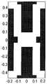
Translated fromKorean도 1은 일반화된 이미지 형성시스템에 대한 투과교차계수함수의 다이어그램,1 is a diagram of a transmission cross-coefficient for a generalized image forming system,
도 2는 브릭벽(brick wall) 아이솔레이션 패턴 마이크로리소그래피 마스크 피처의 예시도,2 is an illustration of a brick wall isolation pattern microlithography mask feature,
도 3은 도 2의 마스크 피처의 회절차수를 표현한 도,3 is a diagram representing diffraction orders of mask features of FIG. 2;
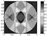
도 4는 도 2의 마스크 피처에 대하여 계산된 최적화된 4차원 조명방식의 맵,4 is a map of an optimized four-dimensional illumination scheme calculated for the mask feature of FIG.
도 5는 도 2의 마스크 피처에 대하여 계산된 스타팅 그레이 스케일(starting gray scale) 조명방식(Jtot)을 나타낸 도,5 is a diagram illustrating a starting gray scale illumination method Jtot calculated for the mask feature of FIG. 2;
도 6은 도 5의 조명방식의 바이너리 표현도,6 is a binary representation of the illumination method of FIG.
도 7은 고리형 조명방식으로 인쇄된 도 2의 마스크 피처의 프린트 분석도,7 is a print analysis diagram of the mask feature of FIG. 2 printed with annular illumination;
도 8은 최적화된 타원형 조명방식으로 인쇄된 도 2의 마스크 피처의 프린트 분석도,8 is a print analysis diagram of the mask feature of FIG. 2 printed with an optimized oval illumination scheme;
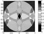
도 9는 110nm 디자인룰로 축척된 도 2의 마스크 피처에 대하여 계산된 최적화된 4차원 조명방식의 맵,9 is an optimized four-dimensional illumination map calculated for the mask feature of FIG. 2 scaled with a 110 nm design rule,
도 10은 110nm 디자인룰로 축척된 도 2의 마스크 피처에 대하여 계산된 스타 팅 그레이 스케일 조명방식을 나타낸 도,FIG. 10 illustrates a starting gray scale illumination scheme calculated for the mask feature of FIG. 2 scaled with a 110 nm design rule. FIG.
도 11a 및 도 11b는 σ값을 다르게 한 도 10의 조명방식의 바이너리 표현도,11A and 11B are binary representations of the illumination scheme of FIG. 10 with σ values different;
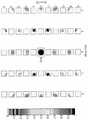
도 12는 지정된 임계 게이트 및 셀을 구비한 마스크 패턴의 예시도,12 is an illustration of a mask pattern with designated threshold gates and cells;
도 13은 패턴내 피치의 수를 줄이기 위해서 어시스트 피처가 첨가된 도 12의 마스크 패턴,FIG. 13 is a mask pattern of FIG. 12 with assist features added to reduce the number of pitches in a pattern; FIG.
도 14는 도 12 및 도 13의 마스크 패턴의 공간폭의 확률밀도함수를 비교한 도,14 is a diagram comparing probability density functions of spatial widths of the mask patterns of FIGS. 12 and 13;
도 15는 마이크로포토리소그래피용 장치의 개략적인 도.15 is a schematic illustration of an apparatus for microphotolithography.
본 발명은 일반적으로 마이크로리소그래피 이미징을 위한 방법 및 장치에 관한 것이다. 특히 본 발명은 이미징된 특정 패턴에 따라 조명방식(illumination configuration)을 최적화하는 장치 및 방법에 관한 것이다. 현재 광 리소그래피 시스템은 집적회로 및 기타 프로그램 가능한 게이트 어레이와 같은 미세 형상제품(fine featured products)의 제조에 사용된다. 가장 일반적인 논의로서, 리소그래피 장치는 방사선의 투영빔을 제공하는 조명시스템, 패터닝수단을 잡아주는 지지구조체, 기판을 잡아주는 기판테이블, 및 기판의 타겟부상으로 패터닝된 빔을 이미징하는 투영시스템(렌즈)을 구비한다.The present invention generally relates to methods and apparatus for microlithography imaging. In particular, the present invention relates to an apparatus and method for optimizing an illumination configuration according to a particular pattern imaged. Optical lithography systems are currently used in the manufacture of fine featured products such as integrated circuits and other programmable gate arrays. In the most general discussion, a lithographic apparatus includes an illumination system for providing a projection beam of radiation, a support structure for holding patterning means, a substrate table for holding a substrate, and a projection system (lens) for imaging the patterned beam onto a target portion of the substrate. It is provided.
패터닝수단(patterning means)이라는 용어는 기판의 타겟부에 형성되어야 할 패턴에 대응하는 패터닝된 단면을 입사하는 방사선 빔에 부여하도록 사용될 수 있는 장치 및 구조체를 의미하는 것으로서 폭넓게 해석되어야 하며, 본 명세서에서는 "광 밸브(light valve)"라는 용어로도 사용된다. 일반적으로, 상기 패턴은 집적회로 또는 기타 디바이스와 같이 타겟부에 형성될 디바이스 내의 특정 기능층에 해당할 것이다.The term patterning means is to be broadly interpreted as meaning an apparatus and structure that can be used to impart a patterned cross section corresponding to a pattern to be formed on a target portion of a substrate to an incident radiation beam, and herein Also used as the term "light valve". In general, the pattern will correspond to a particular functional layer in the device to be formed in the target portion, such as an integrated circuit or other device.
그러한 장치의 일례로서, 일반적으로 (가동) 마스크테이블에 의하여 잡혀있는 마스크가 있다. 마스크의 개념은 리소그래피 분야에서 이미 잘 알려져 있고, 바이너리(binary)형, 교번 위상반전(alternating phase-shift)형, 및 감쇠 위상반전형 마스크뿐만이 아닌 다양한 하이브리드 마스크 형식도 포함된다. 투영빔 내에 이러한 마스크가 놓이면, 마스크의 패턴에 따라 마스크에 입사되는 방사선의 선택적인 투과(투과 마스크의 경우) 또는 반사(반사 마스크의 경우)가 이루어진다. 마스크테이블은 입사되는 투영빔 내의 소정 위치에 마스크가 유지될 수 있게 하며, 필요한 경우에는 마스크가 상기 빔에 대하여 상대적으로 이동될 수 있게 한다.One example of such a device is a mask generally held by a (movable) mask table. The concept of a mask is already well known in the lithography field and includes various hybrid mask types as well as binary, alternating phase-shift, and attenuated phase inverted masks. When such a mask is placed in the projection beam, selective transmission (in the case of a transmission mask) or reflection (in the case of a reflection mask) of radiation incident on the mask is made according to the pattern of the mask. The mask table allows the mask to be held at a predetermined position in the incident projection beam and, if necessary, to allow the mask to be moved relative to the beam.
그러한 장치의 다른 예로서, 점탄성 제어층(viscoelastic control layer) 및 반사면을 구비한 매트릭스-어드레서블면(matrix-addressable surface)이 있다. 이러한 장치의 기본원리는, (예를 들어) 반사면의 어드레스된 영역(addressed area)은 입사광을 회절광으로 반사하는 한편, 어드레스되지 않은 영역은 입사광을 비회절광으로 반사하는 것이다. 적절한 필터를 사용하면, 반사된 빔 중에서 상기 비회절광을 필터링하여 회절광만 남게 할 수 있다. 이러한 방식으로, 빔은 매트릭스-어드레서블면의 어드레싱 패턴에 따라 패터닝된다. 프로그램가능한 거울배열의 대 안적인 실시예는 적절히 국부화된 전계를 가하거나 압전작동수단(piezoelectric actuation mean)을 채용하여 축을 중심으로 각각의 거울이 개별적으로 기울어질 수 있는 작은 거울들의 매트릭스 구성을 채용하는 것이다. 마찬가지로, 상기 거울도 매트릭스-어드레서블으로서, 어드레스된 거울은 입사되는 방사선빔을 어드레스되지 않은 거울과는 다른 방향으로 반사한다. 이러한 방식으로, 반사된 빔은 매트릭스-어드레서블 거울의 어드레싱 패턴에 따라 패터닝된다. 이때 요구되는 매트릭스 어스레싱은 적절한 전자수단을 사용하여 수행될 수 있다. 상기에 서술된 두 가지 상황 모두에서, 패터닝수단은 1이상의 프로그램 가능한 거울배열을 포함할 수 있다. 여기에 언급된 바와 같은 거울배열에 관한 더 많은 정보는, 예를 들어 본 명세서에서 참고 자료로 채용되고 있는, 미국특허 US 5,296,891호, US 5,523,193호 및 PCT 특허출원 WO 98/38597호 및 WO 98/33096호로부터 얻을 수 있다. 프로그램가능한 거울배열의 경우, 상기 지지구조체는 예를 들어, 필요에 따라 고정되거나 움직일 수 있는 프레임 또는 테이블로 구현될 수 있다.Another example of such a device is a matrix-addressable surface with a viscoelastic control layer and a reflective surface. The basic principle of such a device is that (eg) the addressed area of the reflecting surface reflects incident light as diffracted light, while the unaddressed area reflects incident light as non-diffracted light. Using an appropriate filter, the undiffracted light can be filtered out of the reflected beam, leaving only the diffracted light behind. In this way, the beam is patterned according to the addressing pattern of the matrix-addressable surface. Alternative embodiments of programmable mirror arrays employ a matrix configuration of small mirrors in which each mirror can be individually tilted about an axis by applying an appropriately localized electric field or employing a piezoelectric actuation mean. It is. Similarly, the mirror is also matrix-addressable, where the addressed mirror reflects the incident radiation beam in a different direction than the unaddressed mirror. In this way, the reflected beam is patterned according to the addressing pattern of the matrix addressable mirror. The required matrix addressing can be performed using suitable electronic means. In both of the situations described above, the patterning means may comprise one or more programmable mirror arrays. More information regarding mirror arrays as mentioned herein can be found, for example, in US Pat. Nos. 5,296,891, 5,523,193 and PCT patent applications WO 98/38597 and WO 98 /, which are incorporated herein by reference. From 33096. In the case of a programmable mirror array, the support structure may be embodied in a frame or table, for example, which may be fixed or movable as required.
또 다른 예로서, 프로그램 가능한 LCD 배열이 있으며 이 경우에도 마찬가지로 지지구조체는 예를 들어, 프레임이나 테이블일 수 있다. 이러한 구조의 일례는 본 명세서에서 참고자료로 채용되고 있는 미국특허 US 5,229,872호에 개시되어 있다.As another example, there is a programmable LCD arrangement in which case the support structure can likewise be a frame or a table, for example. An example of such a structure is disclosed in US Pat. No. 5,229,872, which is incorporated herein by reference.
설명을 간단히 하기 위하여, 본 명세서의 나머지 부분 중 어느 곳에서는 그 자체가 마스크를 포함하는 예시적인 용어로서 지칭될 수도 있다. 하지만, 그러한 예시에서 논의되는 일반적인 원리는 상술한 바와 같은 패터닝수단의 광의의 개념으 로 이해되어야 한다.For simplicity of explanation, any of the remainder of this specification may, by itself, be referred to as an exemplary term that includes a mask. However, the general principles discussed in such examples should be understood as the broad concept of the patterning means as described above.
투영시스템이라는 용어는 다양한 형식의 투영시스템을 포괄하는 것이다. 일반인들의 관념상 보통 "렌즈"는 굴절광학기만을 의미하지만, 여기에서는 광의로 사용되어 예를 들어, 커탑트릭(catoptric) 및 커타디옵트릭(catadioptric) 시스템을 포함한다. 조명시스템은 투영빔의 지향, 성형 및 제어를 위한 원리들 중 어느 것에 따라 작동하는 요소들을 포함할 수 있고, 이하에서 그러한 요소들을 집합적으로 또는 단독으로 "렌즈"라 칭할 수 있다.The term projection system encompasses various types of projection systems. In general, "lens" usually refers to refractive optics, but is used broadly here to include, for example, catatoptric and catadioptric systems. The illumination system may include elements that operate in accordance with any of the principles for directing, shaping and controlling the projection beam, and hereinafter such elements may be referred to collectively or alone as "lenses."
덧붙여, "웨이퍼테이블"이라는 용어는 이미지를 받아들이는 기판이 실리콘 웨이퍼임을 의미한다기 보다는, 리소그래피장치에 의하여 처리될 어떤 기판을 지지하기에 알맞은 스테이지를 가리키는 것이다.In addition, the term "wafer table" does not mean that the substrate receiving the image is a silicon wafer, but rather refers to a stage suitable for supporting any substrate to be processed by the lithographic apparatus.
예컨대, 리소그래피 투영장치는 집적회로(IC)의 제조에 사용될 수 있다. 이러한 경우, 패터닝수단은 IC의 각각의 층에 대응하는 회로패턴을 생성할 수 있으며, 상기 패턴은 한 층의 방사선감응재(레지스트)로 코팅된 기판(실리콘 웨이퍼)상의 타겟부(1이상의 다이로 구성되는)에 이미징될 수 있다. 일반적으로 한 장의 웨이퍼에는 투영시스템을 통해 한번에 하나씩 연속적으로 조사되는 인접한 타겟부들의 네트워크가 있다. 현재 통용되는 장치에서, 마스크테이블상의 마스크에 의한 패터닝을 채택하는 데에는, 두 가지 서로 다른 형식의 기계로 구분될 수 있다. 특정 형태의 리소그래피 투영장치에서는 타겟부상에 있는 전체 마스크패턴을 한번에 노광함으로써 각 타겟부가 조사되는데, 이러한 장치를 통상 웨이퍼 스테퍼(wafer stepper)라고 한다. 통상, 스텝-앤드-스캔 장치(step-and-scan apparatus)라고 불리워지는 대체 장치에서는 투영빔 하에서 소정의 기준 방향("스캐닝" 방향)으로 레티클 패턴을 점진적으로 스캐닝하는 한편, 상기 스캐닝방향과 같은 방향 또는 반대 방향으로 기판을 동기화시켜 스캐닝함으로써 각 타겟부가 조사된다. 일반적으로 투영시스템은 배율 인자 M(일반적으로 <1)을 가지므로 기판테이블이 스캐닝되는 속도(V)는 마스크테이블이 스캐닝되는 속도의 인자 M배가 된다. 여기에 서술된 리소그래피 장치와 관련된 보다 상세한 정보는 예를 들어, US 6,046,792호로부터 얻을 수 있으며 본 명세서에서도 참조자료로 채용된다.Lithographic projection apparatus can be used, for example, in the manufacture of integrated circuits (ICs). In such a case, the patterning means may generate a circuit pattern corresponding to each layer of the IC, which pattern is formed into a target portion (one or more dies) on a substrate (silicon wafer) coated with a layer of radiation sensitive material (resist). Configured). Typically, one wafer has a network of adjacent target portions that are irradiated one at a time through the projection system. In today's devices, the adoption of patterning by masks on a mask table can be divided into two different types of machines. In a particular type of lithographic projection apparatus, each target portion is irradiated by exposing the entire mask pattern on the target portion at one time. Such an apparatus is commonly referred to as a wafer stepper. An alternative apparatus, commonly referred to as a step-and-scan apparatus, progressively scans the reticle pattern under a projection beam in a predetermined reference direction ("scanning" direction), while the same as the scanning direction. Each target portion is irradiated by synchronously scanning the substrate in the opposite or opposite direction. Since the projection system generally has a magnification factor M (generally <1), the speed V at which the substrate table is scanned is a factor M times that at which the mask table is scanned. More detailed information relating to the lithographic apparatus described herein can be obtained, for example, from US Pat. No. 6,046,792, which is also incorporated herein by reference.
리소그래피 투영장치를 사용하는 제조공정에서, (예를 들어, 마스크)의 패턴은 한 층의 방사선감응재(레지스트)가 최소한의 부분에라도 도포된 기판상에 이미징된다. 이 이미징 단계에 앞서, 기판은 전처리(priming), 레지스트 도포 및 소프트 베이크와 같은 여러가지 과정을 거칠 수 있다. 노광 후에는, 노광후 베이크(PEB), 현상, 하드 베이크 및 이미징된 피처의 측정/검사와 같은 또 다른 과정을 거치게 된다. 이러한 일련의 과정은, 예를 들어 IC 디바이스의 각각의 층을 패터닝하는 기초로서 사용된다. 그 후, 이렇게 패터닝된 층은 에칭, 이온 주입(도핑), 금속화, 산화, 화학-기계적 폴리싱 등과 같은, 각각의 층을 마무르기 위한 여러 공정을 거친다. 여러 개의 층이 요구된다면, 새로운 층마다 전체 공정 또는 그것의 변형된 공정이 반복되어져야만 할 것이다. 그 결과로, 기판(웨이퍼)상에는 디바이스의 배열이 존재하게 될 것이다. 이들 디바이스는 다이싱 또는 소잉 등의 기술에 의하여 서로 분리되고, 이들 각각의 디바이스는 캐리어에 탑재되고 핀에 연결될 수 있다. 이와 같은 공정에 관한 추가 정보는, 예를 들어, 본 명세서에서 참고자료로 채용되고 있는 "Microchip Fabrication: A Practical Guide to Semiconductor Processing"(3판, Peter van Zant 저, McGraw Hill출판사, 1997, ISBN 0-07-067250-4)로부터 얻을 수 있다.In a manufacturing process using a lithographic projection apparatus, a pattern of (e.g., a mask) is imaged on a substrate on which a layer of radiation sensitive material (resist) is applied even at a minimum. Prior to this imaging step, the substrate may be subjected to various processes such as priming, resist application and soft bake. After exposure, there is another process such as post-exposure bake (PEB), development, hard bake, and measurement / inspection of the imaged features. This series of procedures is used, for example, as the basis for patterning each layer of the IC device. The patterned layer is then subjected to several processes to finish each layer, such as etching, ion implantation (doping), metallization, oxidation, chemical-mechanical polishing, and the like. If several layers are required, the whole process or its modified process will have to be repeated for each new layer. As a result, there will be an arrangement of devices on the substrate (wafer). These devices are separated from each other by techniques such as dicing or sawing, and each of these devices can be mounted on a carrier and connected to a pin. Additional information regarding such a process can be found, for example, in "Microchip Fabrication: A Practical Guide to Semiconductor Processing" (3rd edition, Peter van Zant, McGraw Hill, 1997, ISBN 0), which is incorporated herein by reference. -07-067250-4).
편의상, 이하에서 상기 투영시스템을 "렌즈"라고 칭할 수 있다. 하지만 이 용어는 예를 들어, 굴절광학, 반사광학 및 커타디옵트릭 시스템을 포함한 다양한 형식의 투영시스템을 내포하는 것으로서 폭넓게 해석되어야 한다. 또한 상기 방사선시스템은 방사선 투영빔의 지향, 성형 또는 제어를 위한 설계방식 중의 어느 것에 따라 동작하는 구성요소를 포함할 수 있고, 이하에서 이러한 구성 요소들을 집합적으로 또는 개별적으로 "렌즈"라고 칭할 수 있다. 나아가, 리소그래피 장치는 2이상의 기판테이블(및/또는 2이상의 마스크테이블)을 구비하는 형태가 될 수도 있다. 이러한 "복수 스테이지" 장치에서는 추가 테이블이 병행으로 사용될 수 있으며, 1이상의 테이블이 노광에서 사용되고 있는 동안 1이상의 다른 테이블에서는 준비작업 단계가 수행될 수 있다. 예를 들어 US 5,969,441호 및 WO 98/40791호에는 듀얼스테이지 리소그래피장치가 개시되어 있으며, 본 명세서에서도 인용 참조되고 있다.For convenience, the projection system may hereinafter be referred to as a "lens." However, the term should be interpreted broadly as encompassing various types of projection systems, including refractive optics, reflective optics, and catadioptric systems, for example. The radiation system may also include components that operate in accordance with any of the design schemes for directing, shaping or controlling the projection beam of radiation, and in the following, these components may be referred to collectively or individually as "lenses". have. Furthermore, the lithographic apparatus may be of a type having two or more substrate tables (and / or two or more mask tables). In such " multiple stage " devices the additional tables can be used in parallel, and preparatory steps can be carried out on one or more tables while one or more other tables are being used for exposure. For example, US Pat. No. 5,969,441 and WO 98/40791 disclose dual stage lithographic apparatus, which are also incorporated herein by reference.
조명시스템이 종래의 조명형태로부터 고리형 및 4중극 조명형태를 거쳐 더 복잡한 조명형태로 발전되어 옴과 동시에 제어 파라미터가 매우 많아졌다. 종래의 조명패턴에서는 광축을 포함하고 있는 원형 면적이 조명되고 패턴의 조절은 외측반경(σr)을 변경하는 것뿐이었다. 고리형 조명은 조명된 링을 정의하기 위해서 내반 경(σe)의 정의를 요구한다. 다중극 패턴의 경우에 제어될 수 있는 파라미터의 수는 계속 증가한다. 4중극 조명형태의 예를 들면, 2개의 반경외에도 극각(pole angle) α는 선택된 내측반경과 외측반경의 사이에서 각각의 극에 대응되는 각을 정의한다.As lighting systems have evolved from conventional lighting to annular and quadrupole lighting to more complex lighting, there are many control parameters. In the conventional illumination pattern, the circular area including the optical axis is illuminated, and the adjustment of the pattern is only to change the outer radius σr . Annular illumination requires the definition of the inner radius σe to define the illuminated ring. In the case of multipole patterns the number of parameters that can be controlled continues to increase. For example in the form of quadrupole illumination, in addition to the two radii, the pole angle α defines the angle corresponding to each pole between the selected inner and outer radii.
뿐만 아니라 마스크 기술도 계속 개발되어 왔다. 바이너리 세기 마스크(binary intensity mask)는 위상반전 마스크 및 기타 고도한 디자인으로 발전되었다. 바이너리 마스크는 이미징하는 방사선을 주어진 지점에서 단순히 투과, 반사 또는 차단하였지만, 위상반전 마스크는 일부 방사선을 감쇠시킬 수도 있고 위상반전을 시킨 후 빛을 투과 또는 반사하거나 투과 및 반사할 수도 있다. 위상반전 마스크는 이미징 방사선의 파장급이나 그보다 작은 피처를 이미징하기 위해서 사용되어 왔는데, 이는 그 해상도에서의 회절효과로 인하여 다른 문제들 중에서도 열악한 콘트라스트 및 엔드오브라인 에러(end-of-line error)를 유발할 수 있기 때문이다.In addition, mask technology has been continuously developed. Binary intensity masks have evolved into phase inversion masks and other advanced designs. Binary masks simply transmit, reflect, or block the radiation being imaged at a given point, but the phase inversion mask may attenuate some radiation and may transmit or reflect or transmit and reflect light after inverting the phase. Phase inversion masks have been used to image wavelengths or smaller features of imaging radiation, which, due to diffraction effects at their resolutions, produce poor contrast and end-of-line errors, among other problems. It can cause.
인쇄된 이미지의 해상도, 초점심도, 콘트라스트 및 기타 특성을 개선하기 위해서 다양한 형태의 조명방식이 사용될 수 있다. 하지만 각각의 조명방식은 불가피한 트레이드오프를 갖고 있다. 예를 들어, 콘트라스트를 향상시키면 초점심도가 희생되어야 한다. 뿐만 아니라, 각각의 마스크의 형태는 이미징될 패턴에 따라 달라지는 성능을 갖는다.Various forms of illumination can be used to improve the resolution, depth of focus, contrast and other characteristics of the printed image. But each lighting method has an inevitable tradeoff. For example, increasing contrast should sacrifice depth of focus. In addition, the shape of each mask has a performance that depends on the pattern to be imaged.
종래에는 웨이퍼상으로 이미징될 주어진 패턴을 위한 최적의 조명모드를 선정하기 위해서, 일련의 테스트 웨이퍼를 노광하고 무작위로 비교하였다. 상기한 바대로, 현대적 조명시스템은 조작할 수 있는 변수의 수가 계속 증가하고 있다. 변수 세팅의 각종 순열이 증가함에 따라, 조명방식의 시행착오적인 최적화에 드는 비용이 매우 증가하고 조명방식 선정의 정량적 방법이 요구된다.In the past, a series of test wafers were exposed and randomly compared to select the optimal illumination mode for a given pattern to be imaged onto the wafer. As noted above, modern lighting systems continue to increase in the number of variables that can be manipulated. As the various permutations of the parameter settings increase, the cost of trial and error optimization of the illumination scheme increases greatly and a quantitative method of illumination scheme selection is required.
상기 검증된 요구 및 기타 사항을 충족시키기 위해서, 본 발명은 선정된 패터닝수단 패턴을 위한 조명 프로파일을 최적화하는 방법으로서,In order to satisfy the above verified requirements and others, the present invention provides a method of optimizing an illumination profile for a selected patterning means pattern,
조명기 및 선정된 패터닝수단 패턴을 구비하는 광학시스템에 대한 투과교차계수함수(transmission cross coefficient function)을 정의하는 단계;Defining a transmission cross coefficient function for an optical system having an illuminator and a predetermined patterning means pattern;
선정된 패턴에 기초한 회절차수의 이미징에 대한 상대적 관련성(relative relevance)을 결정하는 단계; 및Determining relative relevance to imaging of diffraction orders based on the selected pattern; And
상기 회절차수의 이미징에 대한 상대적 관련성에 기초한 조명방식의 영역에 가중치를 주면서 상기 투과교차계수함수로부터 최적화된 조명방식을 계산하는 단계를 포함하는 방법을 제공한다.Calculating an optimized illumination scheme from the transmission cross-coefficient, while weighting an area of illumination scheme based on the relative relevance to the imaging of the diffraction orders.
본 발명의 또 다른 실시형태에 따르면,According to another embodiment of the present invention,
(a) 적어도 부분적으로는 한 층의 방사선감응재로 도포된 기판을 제공하는 단계;(a) providing a substrate coated at least in part with a layer of radiation sensitive material;
(b) 조명시스템을 사용하여 방사선의 투영빔을 제공하는 단계;(b) providing a projection beam of radiation using an illumination system;
(c) 투영빔의 단면에 패턴을 부여하도록 패터닝수단을 사용하는 단계; 및(c) using patterning means to impart a pattern to the cross section of the projection beam; And
(d) 방사선감응재 층의 타겟부상으로 방사선의 패터닝된 빔을 투영하는 단계를 포함하며, (d) 단계 이전에 상술한 바와 같은 방법을 사용하여 (b) 단계에서 생성된 투영빔의 단면세기분포가 (c) 단계에서 채용된 패턴에 맞추어지는 것을 특징으로 하는 디바이스 제조방법이 제공된다.(d) projecting the patterned beam of radiation onto the target portion of the layer of radiation sensitive material, wherein (d) using a method as described above prior to step (d) and the cross-sectional intensity of the projection beam produced in step (b) A device manufacturing method is provided, characterized in that the distribution is adapted to the pattern employed in step (c).
본 발명의 또 다른 실시형태에 따르면,According to another embodiment of the present invention,
- 방사선의 투영빔을 제공하는 조명시스템;An illumination system providing a projection beam of radiation;
- 소정 패턴에 따라 투영빔을 패터닝하는 역할을 하는 패터닝수단을 지지하는 지지구조체;A support structure for supporting patterning means, the patterning means serving to pattern the projection beam according to a predetermined pattern;
- 기판을 잡아주는 기판테이블; 및A substrate table for holding a substrate; And
- 기판의 타겟부상으로 패터닝된 빔을 투영하는 투영시스템을 포함하는 리소그래피 투영장치로서,A lithographic projection apparatus comprising a projection system for projecting a patterned beam onto a target portion of a substrate,
- 조명기와 소정 패턴에 대한 투과교차계수함수를 정의하고, 상기 패터닝수단에 의하여 생성된 패턴에 기초한 회절차수의 이미징에 대한 상대적 관련성을 결정하며, 상기 회절차수의 이미징에 대한 상대적 관련성에 기초한 조명방식의 영역에 가중치를 주면서 상기 투과교차계수함수로부터 최적화된 조명방식을 계산하는 계산수단,Define a transmissive cross-coefficient function for the illuminator and the predetermined pattern, determine the relative relevance for imaging of the diffraction orders based on the pattern generated by the patterning means, and based on the relative relevance for imaging of the diffraction orders Calculation means for calculating an optimized illumination method from the transmission cross-coefficient while giving weight to an area of an illumination method;
- 상기 계산수단에 의하여 계산된 조명방식에 따라 상기 조명시스템에서 나오는 투영빔의 단면세기분포를 선정하는 선정수단을 더욱 포함하는 것을 특징으로 하는 리소그래피 투영장치가 제공된다.A lithographic projection apparatus further comprising selection means for selecting a cross-sectional intensity distribution of the projection beam exiting the illumination system according to the illumination scheme calculated by the calculation means.
본 발명의 또 다른 실시형태에 따르면, 선정된 마스크 디자인을 최적화하는 방법으로서,According to another embodiment of the invention, as a method of optimizing a selected mask design,
선정된 마스크 디자인의 임계 피처를 검증(identifying)하는 단계;Identifying critical features of the selected mask design;
상기 임계 피처의 회절차수에 기초한 최적화된 조명 프로파일을 결정하는 단계; 및Determining an optimized illumination profile based on the diffraction orders of the critical features; And
선정된 마스크 디자인에 존재하는 피치의 수를 줄이도록 선정된 광근접성 교정법(optical proximity correction method)을 사용하여 선정된 마스크 디자인을 수정하는 단계를 포함하는 방법이 제공된다.A method is provided that includes modifying a selected mask design using a selected optical proximity correction method to reduce the number of pitches present in the selected mask design.
또한 본 발명은 상술한 방법을 실행하는 컴퓨터 프로그램을 제공한다.The present invention also provides a computer program for executing the above method.
본 발명에 따른 장치를 사용함에 있어 본 명세서에서는 IC의 제조에 대해서만 언급하였으나, 이러한 장치가 그 밖에도 다른 가능한 응용례를 가지고 있음은 명백히 이해되어야 한다. 예를 들어, 상기 장치는 집적광학시스템, 자기영역메모리용 유도 및 검출 패턴, 액정표시패널, 박막자기헤드 등의 제조에도 이용될 수 있다. 당업자라면, 전술한 기타 응용분야들을 고려할 때, 본 명세서에서 사용된 "레티클", "웨이퍼" 또는 "다이"와 같은 용어가 "마스크", "기판" 및 "타겟부" 등과 같은 좀 더 일반적인 용어로 각각 대체될 수 있음이 이해될 것이다.In the use of the device according to the present invention only reference is made to the manufacture of the IC, but it should be clearly understood that such devices have other possible applications. For example, the apparatus may be used for manufacturing integrated optical systems, induction and detection patterns for magnetic area memories, liquid crystal display panels, thin film magnetic heads, and the like. Those skilled in the art, given the above-mentioned other applications, the terms "reticle", "wafer" or "die" as used herein are more general terms such as "mask", "substrate" and "target portion", and the like. It will be understood that each can be replaced with.
이하, 첨부된 도면과 예시적인 실시예를 참고로 본 발명을 상세히 서술한다.Hereinafter, the present invention will be described in detail with reference to the accompanying drawings and exemplary embodiments.
본 발명은 조명원 및 패턴 디테일을 산입하여 (마스크로부터) 기판상으로 패턴의 이미징을 우선 수학적으로 모델링하게 한다.The present invention incorporates illumination sources and pattern details to first mathematically model the imaging of the pattern onto the substrate (from the mask).
유한 조명원에 대한 에어리얼 이미지를 계산하는 데에는 두 가지 일차적인 방법이 있다. 그 두 가지 방법은 아베공식(Abbe's formulaion)과 홉킨스공식이다. 아베공식에서는 조명방식내 각 점원(point source)이 패턴상으로 입사하는 평면파를 만들고, 이들 점원의 각각이 웨이퍼상으로 이미징된다. 상기 점원은 공간적으로 인코히런트하므로, 웨이퍼에서의 총 세기는 그들 점원의 각각에 의하여 생성된 세기의 합이다. 따라서, 아베공식에서는 패턴에 대하여 적분한 후 조명방식에 대한 적분이 실행된다.There are two primary methods for calculating aerial images for finite light sources. The two methods are Abbe's formula and Hopkins formula. In Abe's formula, each point source in the illumination system generates a plane wave that is incident on the pattern, and each of these point sources is imaged onto a wafer. Since the point sources are spatially incoherent, the total intensity at the wafer is the sum of the intensities produced by each of those point sources. Therefore, in the Abe formula, the integration of the illumination method is performed after integrating the pattern.
홉킨스공식에서는 적분의 순서가 바뀐다. 즉, 우선 점원에 대한 적분이 실행된다. 홉킨스공식에서는 4차원 투과교차계수(TCC)가 정의되고 이미지 세기는 그 TCC의 역푸리에변환이다. TCC의 유도는 예를 들어, Born and Wolf의Principles of Optics(제6판, pp. 528-532)에 서술되어 있으며, 본 명세서에서 참고자료로 인용된다.In Hopkins' formula, the order of integration is reversed. In other words, the integration to the clerk is executed first. In Hopkins's equation, a four-dimensional transmission cross-coefficient (TCC) is defined and the image intensity is the inverse Fourier transform of that TCC. Derivation of TCC is described, for example, inPrinciples of Optics (6th edition, pp. 528-532) by Born and Wolf, which is incorporated herein by reference.
TCC는 조명 퓨필을 곱한 투영 퓨필의 자동상관관계(autocorrelation)이다. 도 1에서 TCC는 1세트의 3개의 중첩원으로 도시된다. 왼 쪽부터 오른 쪽으로, 첫 번째 원은 조명 퓨필 Js(α, β)을 나타내며, 여기에서 α 및 β는 조명방식의 좌표이다. 다음의 계산을 위해서, Js 의 반경은 예를 들어, 이미징에 사용될 리소그래피 장치에 대하여 최대 허용가능한 외측 σr 로 설정될 수 있다. 실행 가능성 검토를 실시하고 더 큰 σr 의 이득을 결정하기 위해서 σr 을 1.0 이상 크게 설정할 수도 있다.TCC is the autocorrelation of the projection pupil multiplied by the illumination pupil. In Figure 1 the TCC is shown as one set of three overlapping circles. From left to right, the first circle represents the illumination pupil Js (α, β), where α and β are the coordinates of the illumination scheme. For the following calculation, the radius of Js can be set to the maximum allowable outer σr for example for the lithographic apparatus to be used for imaging. In order to conduct a feasibility study and determine the gain of the larger σr , σr may be set larger than 1.0.
중앙의 원은 (-mλ/PxNA, -nλ/PyNA)에 중심을 둔 투영 퓨필 K(α, β)이다. 상기 좌표계는 λ/NA 의 인자로 정규화되어 K의 반경은 1.0 이다. 시계방향 오른 쪽에 있는 원은 투영퓨필을 나타내며, 그 중심은 (pλ/PxNA, qλ/PyNA)에 있다. 나중에 있는 이들 두 표현식에서, m, n, p, 및 q 는 이산 회절차수(discrete diffraction order)에 대응하며 TCC는 상술한 4차원(4-D)식임이 명확해진다. x-방향에서의 회절차수는 m 및 p 로 표현되며, y-방향에서의 회절차수는 n 및 q 로 표현된다. 여기에서는 서술 목적상 x 및 y 좌표가 사용되었지만, 당업자라면 다음의 수학식들에서 좌표계의 적절한 변화를 통하여 대안적인 좌표계가 사용될 수 있음을 알 수 있다.The center circle is the projection pupil K (α, β) centered on (-mλ / Px NA, -nλ / Py NA). The coordinate system is normalized by the factor of λ / NA so that the radius of K is 1.0. The circle clockwise to the right represents the projection pupil, the center of which is at (pλ / Px NA, qλ / Py NA). In these two expressions later on, it is clear that m, n, p, and q correspond to discrete diffraction orders and the TCC is a four-dimensional (4-D) expression described above. The diffraction orders in the x-direction are represented by m and p, and the diffraction orders in the y-direction are represented by n and q. Although x and y coordinates are used here for the purpose of description, those skilled in the art can recognize that alternative coordinate systems may be used through appropriate changes in the coordinate system in the following equations.
4-D 이산점(m,n,p,q)에 대한 TCC는 3개의 원이 모두 중첩된, 음영처리된 면적의 적분이다. 상기 구조는 주기적일 것으로 가정되므로, 상기 패턴의 푸리에변환은 이산하며 TCC는 이산한다. 연속적 패턴 이미지의 경우에, 인접한 피처가 대상이 되는 패턴의 푸리에변환에 영향을 미치지 않을 때까지 피치가 증가될 수 있다. 도 1에서의 TCC는 수학식 1에서 수학적으로 기술된다.The TCC for the 4-D discrete points (m, n, p, q) is the integration of the shaded area with all three circles superimposed. Since the structure is assumed to be periodic, the Fourier transform of the pattern is discrete and the TCC is discrete. In the case of a continuous pattern image, the pitch may be increased until adjacent features do not affect the Fourier transform of the target pattern. The TCC in FIG. 1 is mathematically described in equation (1).

상기 TCC는 회절차수교차계수(DOCC)를 정의함으로써 패턴의 영향을 포함하도록 확장될 수 있다. DOCC는 TCC를 패턴의 푸리에변환계수로 곱하여 유도된 수학식 2에서 정의된다.The TCC can be extended to include the effect of the pattern by defining a diffraction order cross coefficient (DOCC). DOCC is defined in

또한, 웨이퍼에서의 방사선 세기는 수학식 3에서와 같이 DOCC의 역푸리에변환으로 계산될 수 있다.In addition, the radiation intensity at the wafer can be calculated by the inverse Fourier transform of the DOCC as shown in equation (3).

부분적으로 투영 광학시스템은 회절차수를 줄여 몇 개의 회절차수만이 계산된 이미지 세기에 중요한, 저통과필터로서 작용한다. 그 결과 TCC는 대역제한함수이다. 최대의 필요 x 및 y 차수는 각각 수학식 4 및 수학식 5에 따라 계산될 수 있다. 각각의 경우에, 음의 차수 및 양의 차수는 모두 예를 들어, m 이 음의 mmax 로부터 양의 mmax 에 이를 것(-mmax ≤m ≤+mmax)을 필요로 한다. 음의 차수와 양의 차수 모두가 필요하므로, TCC의 크기는 (2mmax+ 1)×(2nmax+ 1)×(2pmax+ 1)×(2qmax+1) 이다. 하지만, 다행히도 TCC는 대역제한이기 때문에 모든 패턴 회절차수를 계산할 필요는 없다. TCC에서와 마찬가지로, x 방향에서는 -mmax ≤m ≤+mmax 의 회절차수만이 필요하고 y 방향에서는 -nmax ≤n ≤+nmax 의 회절차수만이 필요하다.In part, the projection optical system reduces the diffraction orders and only a few diffraction orders act as low pass filters, which are important for the calculated image intensity. As a result, TCC is a band limit function. The maximum required x and y orders can be calculated according to equations (4) and (5), respectively. In each case, both the negative and positive orders both require that m range from negative mmax to positive mmax (-mmax ≦ m ≦ + mmax ), for example. Since both negative and positive orders are required, the size of the TCC is (2mmax + 1) x (2nmax + 1) x (2pmax + 1) x (2qmax +1). Fortunately, however, because TCC is band-limited, it is not necessary to calculate all pattern diffraction orders. As in the TCC, only the diffraction orders of -mmax ≤ m ≤ + mmax are needed in the x direction and only the diffraction orders of -nmax ≤ n ≤ + nmax in the y direction.


수학식 3에 수학식 1 및 2를 대입하면 웨이퍼에서의 방사선 세기에 대한 수학식 6이 주어진다. 수학식 7에 보인 바와 같이 적분의 순서를 바꾸면 즉, 홉킨스공식이 아닌 아베공식을 사용하면, 이미징에 가장 영향을 미치는 조명 퓨필의 부분이 결정될 수 있다. 수학식 6 및 수학식 7은 각각 두 줄에 걸쳐 있다.Substituting


α및 β는 조명 퓨필 좌표를 표현하므로, 새로운 함수 Jopt가 정의될 수 있 다. 새로운 함수 Jopt 는 조명방식(α,β)의 부분이 주어진 회절차수(m,n,p,q)에 대하여 사용되고 있음을 가리키며 수학식 8로 표현된다. 수학식 8로부터, 그것을 역푸리에계수(eikx)로 곱하고 수학식 9에서와 같이 모든 6개의 변수(m,n,p,q,α,β)에 대하여 더함으로써 이미지 세기가 계산될 수 있다.Since α and β represent illumination pupil coordinates, a new function Jopt can be defined. The new function Jopt indicates that part of the illumination scheme (α, β) is used for a given diffraction order (m, n, p, q) and is represented by Equation (8). From equation (8), the image intensity can be calculated by multiplying it by the inverse Fourier coefficient (eikx ) andadding it to all six variables (m, n, p, q, α, β) as in equation (9).


이제 알 수 있듯이, Jopt 는 6차원함수이며 따라서 그것을 조명방식에 적용시키기는 어렵다. 조명방식의 어느 부분에 이미지 형식에 유효한지에 대한 최선의 결정을 위해서는 6개의 변수 중 몇 개를 소거해야 한다.As you can see, Jopt is a six-dimensional function, so it is difficult to apply it to lighting. For the best decision as to which part of the lighting scheme is valid for the image format, some of the six variables must be eliminated.
에어리얼 이미지 세기 I(x,y)는 m+p 및 n+q 에 대한 역변환을 취함으로써 알아낸다. m+p=n+q=0 이면, 에어리얼 이미지 세기에서의 변조(modulation)는 없다. 조명 최적화의 목표 중 하나는 조명방식 중 변조에 영향을 미치지 않거나 거의 미치지 않는 부분을 제거하는 데 있으므로, m+p = n+q = 0 인 경우에 대한 조명방식의 이들 부분들은 제거될 수 있다. 이들 부분을 제거하고 이미지 형식에 유효한 조명방식 부분을 더 가시화하기 위해서, 변수들의 변환은 6차원 Jopt 함수(4개의 회 절차수)에서 2개의 변수를 소거하고 그것을 4차원함수(2개의 회절차수)로 바꾼다. 4차원함수를 Jopt-2D라고 한다. I(x,y)에 대하여, 수학식 9에 수학식 10 및 11을 대입하면, 수학식 12가 도출된다.The aerial image intensity I (x, y) is found by taking the inverse transforms for m + p and n + q. If m + p = n + q = 0, there is no modulation in the aerial image intensity. One of the goals of the lighting optimization is to remove portions of the illumination that have little or no effect on modulation, so that these portions of the illumination for the case of m + p = n + q = 0 can be eliminated. In order to eliminate these parts and further visualize the lighting schemes that are valid for the image format, the transformation of the variables eliminates the two variables in the six-dimensional Jopt function (four times the procedure) and converts them to four-dimensional functions (two diffraction differences). Number). The four-dimensional function is called Jopt-2D . For I (x, y), equations (10) and (11) are substituted into equation (9), where equation (12) is derived.


수학식 12에서, Jopt-2D 는 수학식 10 및 11에 따른 변수의 변환 후 m 및 n 에 대한 Jopt 의 합인 것을 알 수 있다. 또한 수학식 12에 수학식 8을 대입하면, Jopt-2D 는 수학식 13으로 표현될 수 있고, 세기 I(x,y)는 수학식 14에서와 같이 Jopt-2D 의 함수로 나타낼 수 있다.In Equation 12, it can be seen that Jopt-2D is the sum of Jopt for m and n after conversion of the variables according to


수치를 구할 때 함수 Jopt-2D 는 조명방식 중 각 회절차수에 대하여 중요한 부부분을 나타낸다. Jopt-2D 는 각 회절차수 T(m,n)에 의한 가중치를 두고 있으므로, 회절차수가 크면 에어리얼 이미지에 미치는 영향이 커진다.In calculating the value, the function Jopt-2D represents the critical fraction for each diffraction order in the illumination system. Since Jopt-2D is weighted by each diffraction order T (m, n), the larger the diffraction order, the greater the influence on the aerial image.
특정 패턴에 대한 최선의 조명방식을 위한 시작점은 Jtot 로 표기될 수 있고 수학식 15에서와 같이 η 및 ξ에 대하여 Jopt-2D 를 합하고 Jopt-2D(α,β,η= 0, ξ= 0)를 빼줌으로써 구해진다. 수학식 15에서 η= 0, ξ= 0 이면 에어리얼 이미지에서의 변조는 없으며, Jopt-2D(α,β,η= 0, ξ= 0) 성분은 0차 또는 DC 광(DC light)을 나타낸다. 이미징에 기여하지 않는 조명내의 점들은 DC 광의 총합을 증가시킨다. 증가된 DC 광은 변조를 유발하지 않아 큰 이득은 없고 더욱이 그것은 초점심도의 감소를 초래할 수 있다.The starting point for the best illumination for a particular pattern can be expressed as Jtot and sum Jopt-2D for η and ξ as shown in equation (15) and Jopt-2D (α, β, η = 0, ξ Is obtained by subtracting = 0). In Equation 15, if η = 0 and ξ = 0, there is no modulation in the aerial image, and the Jopt-2D (α, β, η = 0, ξ = 0) component represents 0th order or DC light. . Points in the illumination that do not contribute to the imaging increase the sum of the DC light. The increased DC light does not cause modulation so there is no great gain and moreover it can lead to a reduction in the depth of focus.
따라서, Jtot에 따른 조명방식은 DC 광의 양을 최소화하고 향상된 프로세스 윈도우를 가져온다. 식 Jtot는 조명의 어느 부분이 이미지 형성에 더 유효한지(또는 덜 유효한지)를 보여주는 데 사용될 수 있다.Thus, the illumination method according to Jtot minimizes the amount of DC light and results in an improved process window. The equation Jtot can be used to show which part of the illumination is more effective (or less effective) for image formation.

조명방식과 패턴은 밀접하므로, 광근접성교정(OPC)의 변화는 회절차수에 영향을 주고 따라서 Jtot 에 영향을 준다. 결과적으로, 시작 조명방식 Jtot 및 패턴에 대한 수정은 OPC 엔진 및 조명 엔진을 사용한 프로세싱의 반복을 통하여 수회에 걸쳐 실행되어야 하며, 이는 당업자라면 이해할 수 있다. 나아가, 패턴과 조명방식도 최적화 소프트웨어로 실행될 수 있는 특별한 이미징기준(초점심도(DOF), 엔드오브라인(EOL), 수차감응도, 등)을 최적화하도록 맞춰질 것이 필요하다. 하지만, OPC 피처보다는 전체로서의 패턴이 최적의 조명방식에 가장 큰 영향력을 가지므로, Jtot은 조명방식과 패턴에 대한 반복을 최적화하는 가장 빠른 수렴을 이끌기에 가장 좋은 처음의 조명방식이다.Since the illumination scheme and the pattern are closely related, the change in the optical proximity correction (OPC) affects the diffractionorders and thus the Jtot . As a result, modifications to the starting illumination Jtot and pattern must be carried out several times through iterations of processing using the OPC engine and the illumination engine, which can be appreciated by those skilled in the art. In addition, patterns and lighting schemes need to be tailored to optimize specific imaging criteria (DOF, End of Brain (EOL), aberration sensitivity, etc.) that can be implemented with optimization software. However, because the pattern as a whole, rather than the OPC feature, has the greatest impact on the optimal illumination, Jtot is the first illumination to lead to the fastest convergence that optimizes the illumination and repetition of the pattern.
시작 조명방식 Jtot 는 0 내지 1 범위에 대한 세기의 연속값을 갖는 그레이 스케일 조명방식으로 표현될 수 있다. 회절 광학요소(DOE) 또는, 디더링된 크롬(dithered choromium)으로 도금된 쿼츠판을 사용함으로써 그러한 그레이 스케일 조명방식을 만들어낼 수 있다. 그레이 스케일 조명방식이 불가능하거나 바람직하지 않다면, 그레이 스케일에 스레스홀드를 적용하여 조명 프로파일이 0 또는 1 만 되도록 강제될 수 있으며 그보다 큰 값에서 스레스홀드는 1로 절상되고 그 보다 작은 값에서 스레스홀드는 0으로 절하된다. 임의의 스레스홀드가 적용될 수도 있 고, 프로세스 윈도우를 시뮬레이션하거나 반복된 테스트 시행을 통하여 최적의 스레스홀드를 알아낼 수도 있다.The starting illumination Jtot can be represented by a gray scale illumination with a continuous value of intensity for the range 0-1. Such gray scale illumination can be achieved by using diffractive optical elements (DOE) or quartz plates plated with dithered chromium. If gray scale illumination is not possible or undesirable, then a threshold can be applied to the gray scale to force the illumination profile to be 0 or 1 only, at higher values the threshold is rounded up to 1 and the threshold at smaller values. The hold is reduced to zero. Any threshold may be applied, or the optimal threshold may be determined by simulating the process window or by repeating test runs.
실험례 1: 상기 약술된 Jtot 를 계산하는 기법을 브릭벽 아이솔레이션 패턴에 적용하였다. 150nm 패턴이 130nm 및 110nm 디자인룰(design rule)로 축소되었고 0.8의 개구수(NA)를 갖는 스텝앤드스캔 리소그래피 시스템으로 이미징되었다. 130nm 디자인룰을 위한 아이솔레이션 패턴은 도 2에 도시되어 있다.Experimental Example 1: The above-described technique for calculating Jtot was applied to a brick wall isolation pattern. The 150 nm pattern was scaled down to 130 nm and 110 nm design rules and imaged with a step-and-scan lithography system with a numerical aperture (NA) of 0.8. The isolation pattern for the 130nm design rule is shown in FIG. 2.
상기 마스크 피처의 회절차수의 크기는 도 3에 도해되어 있다. 도 3에서 가장 큰 차수는 (0,0)차 또는 DC 배경광(DC background light)이다. 이미징에 가장 크게 기여하는 차수는 (±2, 0)차수이며 브릭벽 패턴내의 수직 브릭을 표현한다. 다른 유효한 차수는 밝은 영역을 표현하며 아이솔레이션 패턴의 끝을 정의하는 (±1, ±1)이다. 더 높은 차수도 각 라인의 끝과 같은 2차원 구조를 정의하는 데 도움을 준다. 회절차수는 일정하지 않으므로 차수는 DOCC 내의 가중치 계수를 변경시키고, 이것은 마스크 패턴이 조명전략에 영향을 준다는 것을 의미한다.The magnitude of the diffraction orders of the mask features is illustrated in FIG. 3. The largest order in FIG. 3 is the (0,0) order or DC background light. The order that contributes most to the imaging is the (± 2, 0) order and represents the vertical brick in the brick wall pattern. Another valid order is (± 1, ± 1), which represents bright areas and defines the end of the isolation pattern. Higher degrees also help define a two-dimensional structure, such as the end of each line. Since the diffraction orders are not constant, the order changes the weighting coefficients in the DOCC, which means that the mask pattern influences the illumination strategy.
도 3에서 회절차수계수 T(m,n)을 수학식 13에 대입하여 Jopt-2D 를 계산할 수 있고 도 4에 도해되어 있다. 도 4로부터 알 수 있듯이, Jopt-2D 에 가장 크게 기여하는 것은 (η= 0, ξ= 0)차수이다. (0,0)차는 이미징에 기여하지 않으며 DOF를 감소시킨다. 수학식 15에 보인 바와 같이, 상기 (0,0)차는 총 조명 Jtot 로부터 차감될 수 있다. (0,0)차를 고려하지 않으면, 가장 큰 기여는 x 방향을 따른 아이솔레이션 라인의 형성을 표현하는 (η= ±2, ξ= 0) 회절차수이다. 크고 아이솔레이션 라인의 끝을 정의하는 또 다른 성분은 (η= ±1, ξ= ±1) 회절차수이다. (0, ±2) 회절차수는 작은 편이지만 더 높은 차수들은 렌즈의 η= 0 및 ξ= ±2 영역에서 결합(combine)한다. 이들 영역도 라인의 끝을 정의하는 데 도움을 준다. DOCC 접근은 조명 퓨필이 향상된 이미지 형성을 위하여 어떻게 샘플링되는지를 보여주며 브릭벽 아이솔레이션 패턴의 이미징을 이해하는 데 효과적인 방법이다.In FIG. 3, Jopt-2D can be calculated by substituting the diffraction coefficient T (m, n) into Equation 13 and illustrated in FIG. 4. As can be seen from FIG. 4, the largest contribution to Jopt-2D is the order (η = 0, ξ = 0). The (0,0) difference does not contribute to imaging and reduces the DOF. As shown in equation (15), the (0,0) difference can be subtracted from the total illumination Jtot . Without considering the (0,0) difference, the largest contribution is the (η = ± 2, ξ = 0) diffraction order, representing the formation of an isolation line along the x direction. Another component that defines the end of a large isolation line is the diffraction order (η = ± 1, ξ = ± 1). The (0, ± 2) diffraction orders are small but higher orders combine in the η = 0 and ξ = ± 2 regions of the lens. These areas also help define the end of the line. The DOCC approach shows how lighting pupils are sampled for improved image formation and is an effective way to understand the imaging of brickwall isolation patterns.
수학식 15를 사용하면, 130nm 디자인룰용 브릭벽 패턴의 조명 퓨필이 계산될 수 있으며 도 5에 도시된다. 도 5는 이미지 형성에 가장 유효한 면적은 x 축을 따른 조명방식의 외측부임을 보여준다. 이들 외측부는 타원형 쌍극을 형성한다. 이들 타원형 쌍극 요소와 더불어 조명 퓨필의 중심은 이미지 포뮬레이션에 큰 기여를 한다. 상기 주지하는 바와 같이, 조명 퓨필은 그레이 스케일이나 바이너리 조명 프로파일에서 구현될 수 있다.Using Equation 15, the illumination pupil of the brickwall pattern for 130 nm design rule can be calculated and shown in FIG. 5 shows that the most effective area for image formation is the outer part of the illumination along the x axis. These outer portions form an elliptical dipole. In addition to these elliptical dipole elements, the center of the illumination pupil makes a significant contribution to the image formulation. As noted above, illumination pupils can be implemented in gray scale or binary illumination profiles.
사용되는 장치에 따라서 크레이 스케일 조명이 가능할 수 있다. 그레이 스케일 조명에 의하여 제어 가능한 조명세기는 적어도 주어진 부분의 조명방식에 대하여 0 내지 1로 그 정규화된 레벨을 선택할 수 있다. 예를 들어, 조명세기에 대한 그러한 제어는 조명시스템내의 회절광학요소(DOE)의 사용으로 생성될 수 있다. 이 경우에, 예를 들어 조명방식은 도 5에 도시된 것처럼 구현될 수 있다. 하지만 이론상 계산되는, 도 5에 보인 일부 로컬 스파이크(local spike)는 상기 논의된 바와 같이 투영광학기의 결과로서 조명 정보의 저통과 필터링후 제거될 것이다. 따라서, 조명방식을 디자인할 때, 필터링될 스파이크는 무시되어야 한다.Depending on the device used, cray scale lighting may be possible. The illumination intensity controllable by gray scale illumination can select its normalized level from 0 to 1 for at least a given part of the illumination scheme. For example, such control over the illumination intensity can be created by the use of diffractive optical elements (DOE) in the illumination system. In this case, for example, the illumination scheme may be implemented as shown in FIG. However, some local spikes shown in FIG. 5, which are theoretically calculated, will be removed after low pass filtering of illumination information as a result of projection optics as discussed above. Therefore, when designing the illumination scheme, the spikes to be filtered must be ignored.
바이너리 조명방식이 사용되는 경우, 즉 조명기의 세기에 2진값만 허용되는(0 또는 1) 경우, 스레스홀드값은 조명방식상의 각 점에 0 또는 1의 값을 할당하는 근거로서 채택되어야 한다. 예를 들어, 0.8의 스레스홀드가 채택되면, 0.8 보다 큰 조명기 세기는 1로 절상되고 0.8 보다 작은 값은 0 으로 절하된다. 그 밖의 스레스홀드 값은 원하는 바대로 적용될 수 있다.If binary illumination is used, i.e. only binary values are allowed (0 or 1) for the intensity of the fixture, the threshold value should be taken as the basis for assigning a value of 0 or 1 to each point on the illumination. For example, if a threshold of 0.8 is adopted, fixture intensities greater than 0.8 are rounded up to 1 and values less than 0.8 are rounded down to zero. Other threshold values can be applied as desired.
실험례 2: 바이너리 접근에 그레이 스케일을 사용하여 동일한 브릭벽 아이솔레이션 패턴에 대한 바이너리 조명방식이 0.88 의 최대 외측 σ로 가정하여 디자인되었고 도 6에 도시되어 있다.Experimental Example 2: A binary illumination scheme for the same brick wall isolation pattern using gray scale for the binary approach was designed assuming a maximum outer sigma of 0.88 and is shown in FIG. 6.
그런 다음, 도 6에서 최적화된 조명방식의 성능은 NA = 0.8 이고 λ= 248nm 를 갖는 스텝앤드스캔 마이크로리소그래피장치상의 바이너리 마스크에 대하여 시뮬레이션되었고 고리형 조명의 성능을 시뮬레이션한 것과 비교하였다. 시뮬레이션에서, 개구수가 0.7 보다 컸으므로 벡터(박막) 이미징 레지스트 모델이 사용되었다. 이 모델에서 레지스트는 굴절율 n = 1.577 - j3.588 을 갖는 폴리실리콘 재료의 상부에 n = 1.45 - j0.3 을 갖는 두께 66nm 의 재료 위에 400nm 두께의 굴절율 n = 1.76 - j0.0116 을 갖는 다른 종류의 재료로 되어 있다. 고리형 조명(σin = 0.58 이고 σout = 0.88) 및 최적화된 조명(σout = 0.88)의 결과가 도 7 및 도 8에 각각 도시된다. 도 7 및 도 8 모두에서 아이솔레이션 영역의 중간에서의 단면 결과 및 상하 시뮬레이션 결과가 도시된다. 상기 도면에서, 레지스트를 거치는 세기를 평균하여 에어리얼 이미지 스레스홀드로부터 보쑹도(Bossung plot) B 가 계산되고, 그 합성 선폭 lw 가 스레스홀드 세기에 대한 포커스 f 에 대하여 도해된다. 이 기 법은 두께 손실 및 레지스트 프로파일 슬로프를 고려해 넣지 않아서 DOF 를 과장되게 예상하기 쉽다. 적어도 두께 손실을 계산하는 레지스트 모델이 필요할 것이다. 각각의 도면에서, 상하(top down) 결과는 보쑹도에서 계산된 최선의 스레스홀드(최적 도즈)에서 실선의 곡선으로 도해되어 있다. 이들 시뮬레이션된 스레스홀드 이미지는 점선의 직선으로 나타낸 실제의 마스크 데이터와 비교된다.Then, the performance of the optimized illumination scheme in FIG. 6 was simulated for a binary mask on a step-and-scan microlithography apparatus with NA = 0.8 and λ = 248 nm and compared with the simulation of the performance of annular illumination. In the simulation, the vector (thin film) imaging resist model was used because the numerical aperture was greater than 0.7. In this model, the resist is another kind of 400 nm thick refractive index n = 1.76-j0.0116 on 66 nm thick material having n = 1.45-j0.3 on top of the polysilicon material with refractive index n = 1.577-j3.588 It is made of material. The results of the annular illumination (σin = 0.58 and sigmaout = 0.88) and optimized illumination (σout = 0.88) are shown in FIGS. 7 and 8, respectively. In both FIG. 7 and FIG. 8, the cross sectional results and the up and down simulation results in the middle of the isolation region are shown. In this figure, the Bossung plot B is calculated from the aerial image thresholds by averaging the intensity across the resist, and its composite linewidth lw is illustrated for the focus f on threshold intensity. This technique does not account for thickness loss and resist profile slopes, making it easier to anticipate DOF. At least a resist model will be needed to calculate the thickness loss. In each figure, the top down results are illustrated by the solid line curve at the best threshold (optimal dose) calculated from the roundness. These simulated threshold images are compared with the actual mask data represented by dashed straight lines.
130nm 디자인룰 브릭벽 아이솔레이션 패턴에 대한 시뮬레이션 결과는 도 7에서 고리형 조명(σin = 0.58 이고 σout = 0.88)을 사용한 0.8 의 NA를 가진 바이너리 마스크 피처에 대하여 도해되어 있다. 이 고리형 세팅은 -0.4㎛ 부터 0.0㎛ 까지의 포커스로 대략 0.4㎛ 의 DOF를 갖는다. 레지스트의 콘트라스트는 포커스 전체에서 낮고, 낮은 콘트라스트 레지스트를 사용하여 이미징될 수 있다. 하지만, 이 낮은 세기 콘트라스트에서 마스크에러 강화인자(mask error enhancement factor; MEEF)는 크고 노광관용도(EL)는 작다. 또한 도 7에서의 상하 이미지는 라인의 끝(EOL)이 대략 20nm 단축됨을 보이며, 이것은 130nm 디자인룰에 대하여 라인을 약간 연장함으로써 바로잡을 수 있다. 하지만 디자인룰이 계속 축소됨에 따라, 연장된 라인이 다른 피처와 충돌할 수 있기 때문에 라인을 연장하는 것은 더이상 실현 불가능하다. 따라서, EOL을 조명을 이용하여 바로잡는 것이 바람직하다.Simulation results for a 130 nm design rule brick wall isolation pattern are illustrated in FIG. 7 for a binary mask feature with an NA of 0.8 using annular illumination (σin = 0.58 and sigmaout = 0.88). This annular setting has a DOF of approximately 0.4 μm with a focus from −0.4 μm to 0.0 μm. The contrast of the resist is low throughout the focus and can be imaged using a low contrast resist. However, in this low intensity contrast, the mask error enhancement factor (MEEF) is large and the exposure latitude (EL) is small. The top and bottom images in FIG. 7 also show that the end of the line (EOL) is shortened by approximately 20 nm, which can be corrected by extending the line slightly for the 130 nm design rule. However, as design rules continue to shrink, extending lines is no longer feasible because extended lines can collide with other features. Therefore, it is desirable to correct the EOL using illumination.
도 8에는 130nm 디자인룰 브릭벽 아이솔레이션 패턴에 대한 시뮬레이션 결과가 도 6의 최적화된 바이너리 조명방식을 사용하여 0.8의 개구수를 가진 바이너리 마스크 피처에 대하여 도해되어 있다. 최적의 조명방식은 -0.45㎛ 부터 +0.15㎛ 까지의 포커스로 대략 0.6㎛ DOF를 갖는다. 도 8의 단면 이미지와 도 7의 그것을 비교할 때, 최적화된 조명방식은 고리형 조명에 비하여 포커스 전체에서 더 큰 콘트라스트를 갖는다. 상기 더 큰 콘트라스트는 최적화된 조명방식에 대한 MEEF가 고리형 조명에 비하여 더 낮다는 것과 최적화된 조명방식의 노광관용도가 더 크다는 것을 의미한다. 최적화된 조명방식의 또 다른 이득은 고리형 조명에 비하여 향상된 라인엔드 성능에 있다. 도 8에서의 상하 이미지는 패턴상의 라인을 연장하지 않고도 최적화된 조명방식이 EOL을 유지할 수 있음을 보이며, 이것은 더 적극적인 디자인룰 축소에 유리하다.In FIG. 8, simulation results for a 130 nm design rule brick wall isolation pattern are illustrated for a binary mask feature with a numerical aperture of 0.8 using the optimized binary illumination scheme of FIG. 6. The optimal illumination method has a roughly 0.6 μm DOF with a focus from −0.45 μm to +0.15 μm. When comparing the cross-sectional image of FIG. 8 with that of FIG. 7, the optimized illumination scheme has greater contrast throughout the focus as compared to annular illumination. The higher contrast means that the MEEF for the optimized illumination is lower than the annular illumination and the exposure latitude for the optimized illumination is greater. Another benefit of optimized lighting is improved line-end performance over annular lighting. The top and bottom image in FIG. 8 shows that the optimized illumination scheme can maintain the EOL without extending the lines on the pattern, which is advantageous for more aggressive design rule reduction.
실험예 3: 바이너리 마스크(BIM)에 대한 도 7 및 도 8의 결과를 무크롬 마스크(CLM)에 대한 시뮬레이션 결과와 비교하였다. 무크롬 브릭벽 아이솔레이션 패턴은 당업자에게 알려져 있는 방식으로 소프트웨어 시뮬레이션의 실험적 결과로부터 디자인되었다. 무크롬 기술은 오프액시스 조명(off-axis illumination)으로 얻어진 DOF 향상으로부터의 충분한 이득을 얻기 위하여 (0,0)차 광을 필요로 한다. 시뮬레이션으로부터의 실험적 결과는 아이솔레이션 층이 디더링(dithered)되거나 하프톤(half toned)되어야 하는 목적을 위하여 (0,0)차 광이 필요함을 입증한다. 하프톤 피치는 디더링된 방향으로의 제1차수가 투영 퓨필에 들어가지 않도록 선택될 수 있다. 본 실험에서, 라인은 수직방향에서 λ/[NA(1+σout)] 보다 작은 피치로 디더링되었다. 하지만 디더링 듀티사이클은 최선의 DOF 및 패턴 충실도(pattern fidelity)를 위하여 (0,0)차 광의 양을 최적화하도록 튜닝되어야 한다. CLM에 대 한 시뮬레이션 결과에서 하프톤 피치는 50% 듀티사이클로 155nm(77.5nm 크롬 섬)이었다. 상기 피치는 실질적으로 (0,±1)차가 투영 퓨필로 들어오지 못하게 한다. 하지만, 상기 듀티사이클은 컴퓨터지원설계(CAD) 도구를 사용하여 최대 DOF로 튜닝되어야 한다.Experimental Example 3: The results of FIGS. 7 and 8 for the binary mask (BIM) were compared with the simulation results for the chromeless mask (CLM). The chrome-free brickwall isolation pattern was designed from the experimental results of software simulation in a manner known to those skilled in the art. The chromium-free technique requires (0,0) order light in order to get sufficient benefit from the DOF improvement obtained with off-axis illumination. Experimental results from the simulation demonstrate that the (0,0) order light is needed for the purpose that the isolation layer should be dithered or halftone. The halftone pitch may be selected such that the first order in the dithered direction does not enter the projection pupil. In this experiment, the lines were dithered with a pitch smaller than λ / [NA (1 + σout )] in the vertical direction. However, the dither duty cycle should be tuned to optimize the amount of (0,0) order light for best DOF and pattern fidelity. In the simulation results for CLM, the halftone pitch was 155 nm (77.5 nm chrome island) with a 50% duty cycle. The pitch substantially prevents (0, ± 1) differences from entering the projection pupil. However, the duty cycle should be tuned to maximum DOF using a computer aided design (CAD) tool.
실험예 4: 130nm 디자인룰 층에 대한 시뮬레이션 결과가 155nm 하프톤 및 50% 듀티사이클을 가진 CLM에 대하여 도해되어 있다. CLM은 0.8의 NA를 가진 λ= 248nm 장치 위에서 고리형 조명(σin = 0.58 이고 σout = 0.88)으로 노광된다. 상기 고리형 세팅으로 CLM은 0.5㎛ DOF (-0.4㎛ 포커스 내지 +0.1㎛ 포거스)를 가졌다. 고리형 조명에 의한 CLM은 고리형 조명에 의한 BIM에 비하여 더 큰 DOF 및 포커스 전체에서 더 우수한 콘트라스트를 가졌다. 이것은 BIM 마스크보다는 CLM이 더 우수하게 실행되었음을 가리킨다. 상하 시뮬레이션 결과는 CLM에 의한 EOL 성능이 이론적으로 BIM에 의한 EOL 성능보다 우수하다는 것과 CLM이 BIM에 비하여 콘택홀 랜딩면적을 더 잘 정의할 수 있다는 것을 알려주었다.Experimental Example 4: Simulation results for a 130 nm design rule layer are illustrated for a CLM with 155 nm halftones and 50% duty cycle. The CLM is exposed to annular illumination (σin = 0.58 and σout = 0.88) on a λ = 248 nm device with an NA of 0.8. In the annular setting, the CLM had a 0.5 μm DOF (−0.4 μm focus to +0.1 μm fogger). CLM with annular illumination had better contrast throughout the focus and greater DOF compared to BIM with annular illumination. This indicates that CLM performed better than BIM mask. The simulation results showed that EOL performance by CLM is theoretically superior to EOL performance by BIM, and that CLM can better define contact hole landing area than BIM.
실험예 5: 130nm 브릭벽 아이솔레이션 패턴 아이솔레이션 층에 대한 시뮬레이션 결과가 0.8의 NA와 도 6에 도시된 최적화된 타원형 쌍극을 가진 λ= 248nm 장치에 대하여 도해되어 있다. 이들 결과는 이전 실험예에서 사용된 CLM 레티클과 동일한, 155nm 하프톤 피치 및 50% 듀티사이클을 가진 레티클로 시뮬레이션되었다. 최적화된 조명방식으로 노광된 CLM은 0.7㎛ DOF (-0.5㎛ 내지 +0.2㎛)를 가져 40%의 향상을 보였다. 보쑹도는 아이소포컬 세기(isofocal intensity)가 대략 0.21 임을 가리켰다. 레티클을 교정 선폭의 크기로 튜닝하여 성능을 더욱 향상시키기 위해서 OPC 접근에 기초한 모델이 추가로 적용될 수 있었다. 선폭은 예를 들어, 하프톤 듀티사이클을 바이어스하고 수정함으로써 교정될 수 있다. 상하 시뮬레이션 결과는 CLM이 콘택트 랜딩영역을 정의할 수 있고 CD 균일성을 유지할 수 있음을 나타내었다. 네킹(necking) 및 기타 선폭 비일관성은 상기 타원형 조명방식에 의하여 감소되었다. 또한, CLM 레티클은 DOF를 향상시키도록 바이어스될 수 있었고 결과적으로 EOL 성능은 향상되었다. 또한, OPC에 기초한 모델은 EOL을 더욱 교정할 수 있었다.Experimental Example 5: Simulation results for a 130 nm brick wall isolation pattern isolation layer are illustrated for a λ = 248 nm device with an NA of 0.8 and the optimized elliptical dipole shown in FIG. 6. These results were simulated with a reticle with a 155 nm halftone pitch and 50% duty cycle, identical to the CLM reticle used in the previous experimental example. The CLM exposed by the optimized illumination method had a 0.7 μm DOF (−0.5 μm to +0.2 μm), showing a 40% improvement. The complementarity indicated that the isofocal intensity was approximately 0.21. In order to further improve performance by tuning the reticle to the size of the calibration line width, an additional model based on the OPC approach could be applied. The line width can be corrected, for example, by biasing and modifying the halftone duty cycle. The top and bottom simulation results show that the CLM can define contact landing areas and maintain CD uniformity. Necking and other linewidth inconsistencies were reduced by the elliptical illumination. In addition, CLM reticles could be biased to improve DOF, resulting in improved EOL performance. In addition, models based on OPC were able to further correct EOL.
실험예 6: 110nm 디자인룰 아이솔레이션 층에 대한 도 2의 마스크 패턴을 사용하여, 수학식 13 및 15에 의하여 최적화된 조명방식이 생성되었다. 조명 퓨필의 샘플링을 가시화하기 위해서, Jopt-2D 가 도 9에 도해되어 있으며 수평으로는 x 차수 (η= m + p)를 나타내고 수직으로는 y 차수(ξ= n + q)를 나타낸다. 도 4의 130nm 디자인룰의 경우에서처럼 도 11의 110nm 디자인룰에 가장 크게 기여하는 것은 (η= 0, ξ= 0)차수이다. 상기 (0, 0)차 광은 DOF에 해로운 영향을 미치며 수학식 15에 표시된 바와 같이 Jtot 에서 제거된다. 또한 도 9는 (±1, ±1)차수가 (±2, 0)차수보다는 조명방식 최적화에 가장 크게 기여함을 보여준다. 이것은 110nm 디자인룰이 NA = 0.8 을 갖는 248nm 장치에 대하여 너무 적극적이라는 사실에 기인하며 이는 그 해상도를 이루기 위해서는 약간 더 큰 NA가 바람직하기 때문이다. 아이솔레이션 선폭을 정의하는 데 가장 크게 기여하는 차수는 (±2, 0)차수이다. 하지만, (±2, 0)차수는 조명방식의 먼 가장자리(0.8 < σ< 1.0)에 있으며 이것은 1의 σ가 그 파장에서 110nm 디자인룰의 구현에 향상을 가져온다는 것을 나타낸다.Experimental Example 6 Using the mask pattern of FIG. 2 for the 110 nm design rule isolation layer, an illumination scheme optimized by Equations 13 and 15 was generated. In order to visualize the sampling of the illumination pupil, Jopt-2D is illustrated in FIG. 9 with the x order (η = m + p) horizontally and the y order (ξ = n + q) horizontally. As in the case of the 130 nm design rule of FIG. 4, the largest contribution to the 110 nm design rule of FIG. 11 is the order (η = 0, ξ = 0). The (0, 0) order light has a detrimental effect on DOF and is removed from Jtot as shown in equation (15). In addition, FIG. 9 shows that the (± 1, ± 1) order contributes more to the lighting system optimization than the (± 2, 0) order. This is due to the fact that the 110 nm design rule is too aggressive for 248 nm devices with NA = 0.8 because slightly larger NAs are desirable to achieve that resolution. The order that contributes the most to defining the isolation line width is the order (± 2, 0). However, the (± 2, 0) order is at the far edge of the illumination scheme (0.8 <σ <1.0), indicating that σ of 1 results in an improvement in the implementation of the 110nm design rule at that wavelength.
수학식 15 및 도 9의 결과를 이용한, 110nm 브릭벽 아이솔레이션 층에 대한 최적화된 조명방식이 도 10에 도시되어 있다. 도 10은 이미지 형성에 가장 크게 기여하는 조명방식 면적이 중심의 작은 부분 및 조명방식의 먼 가장자리임을 보인다. 이 조명방식의 한 가지 가능한 구현방법이 도 11a에 도해되어 있다. 더 적극적인 디자인룰을 인쇄하고 투영 개구수의 한계를 넓히도록 248nm 장치를 사용하기 위해서, 도 11b에 도시된 바와 같이 1.0의 σ를 갖고 작은 섹터(0.2의 σ링폭)을 갖는 조명방식이 사용될 수 있다.An optimized illumination scheme for a 110 nm brick wall isolation layer, using the results of Equations 15 and 9 is shown in FIG. 10. 10 shows that the illumination area that contributes the most to image formation is a small portion in the center and the far edge of the illumination method. One possible implementation of this illumination scheme is illustrated in FIG. 11A. In order to print more aggressive design rules and use the 248nm device to widen the projection numerical aperture, an illumination scheme having a small sector (σ ring width of 0.2) and having a sigma of 1.0 as shown in FIG. 11B can be used. .
본 발명의 구현방법에는 임계적 셀 또는 특정 게이트의 선택이 포함된다. 이들 임계 피처는 그 후 상기 서술된 Jtot을 결정하도록 처리된다. 섹션 1에서, 조명방식은 패턴 의존적임을 보였다. 따라서, 피치가 임계 피처의 경우와 확연히 다르지 않다면 모든 임계 피처에 대한 프로세스 윈도우를 최적화하는 단일 조명방식을 만들어낼 수 있다. 도 12에는 임계적 게이트(g1, g2, g3) 및 임계적 셀(cc)을 구비한 회로의 예가 도시되어 있다. 이들 태그된 임계 피처의 회절차수는 계산될 수 있으며, 이미 서술된 이론을 이용하여 최적화된 조명방식이 계산될 수 있다. 최적화된 조명방식을 계산한 후에는 프로세스 윈도우가 계산될 수 있고 다른 조명방식에 의한 프로세스 윈도우와 비교할 수 있다.Implementations of the invention include the selection of critical cells or specific gates. These critical features are then processed to determine the Jtot described above. In
조명/패턴 상호작용을 최적화하는 또 다른 방법은 스캐터링 바(scattering bar)로 패턴디자인을 수정하는 것이다. 스캐터링 바는 ASIC 또는 로직 디자인에 대한 준연속함수(semicontinuous function)로부터 피치를 이산시킨다. 스캐터링 바를 배치하면 피치의 수가 적어진다. 이것은 0.61λ/NA 의 에지 대 에지 분리로 스캐터링 바를 배치함으로써 시뮬레이션 소프트웨어에서 입증될 수 있다. 도 13에서, 도 12의 디자인은 복수의 스캐터링 바를 부가함으로써 수정되었다. 그러면 조명방식은 수정된 디자인에 대하여 최적화될 수 있다. 그러면 스캐터링 바를 갖는 디자인에 대하여 최적화된 조명방식의 프로세스 윈도우 성능은 스캐터링 바가 없이 최적화된 조명방식의 프로세스 윈도우와 비교될 수 있다. 스캐터링 바를 갖는 디자인은 피치를 이산시키므로, 최적화된 오프액시스 조명(OAI)과 스캐터링 바의 결합은 가능성이 가장 큰 DOF 프로세스 윈도우를 가질 것이다.Another way to optimize lighting / pattern interactions is to modify the pattern design with a scattering bar. The scattering bar discretes the pitch from a semicontinuous function for an ASIC or logic design. Placing scattering bars reduces the number of pitches. This can be demonstrated in the simulation software by placing scattering bars with edge to edge separation of 0.61λ / NA. In FIG. 13, the design of FIG. 12 was modified by adding a plurality of scattering bars. The illumination can then be optimized for the modified design. The illumination process window performance optimized for a design with scattering bars can then be compared with the optimization illumination process window without scattering bars. Since designs with scattering bars are discrete in pitch, the combination of optimized off axis illumination (OAI) and scattering bars will have the most likely DOF process window.
조명방식 최적화를 구현하는 또 다른 개념은 공간폭(SW) 고려에 기초한 스캐터링 바의 배치를 통한 것이다. 스캐터링 바는 공간 폭으로 규칙이 정의될 수 있는 OPC계 규칙을 따라 배치된다. 시뮬레이션 소프트웨어로 스캐터링 바가 없는 공간폭과 스캐터링 바를 가진 공간폭의 확률밀도함수(pdf)를 계산할 수 있다. 그러면 조명은 상기 pdf를 고려하여 수학식 16에 보인 Jopt-2D 를 수정함으로써 최적화될 수 있다. 수직 라인과 수평 라인이 유한하다고 가정하면 회절차수 T(m,n)을 계산하는 것도 가능하다. 수학식 17에서, w를 선폭이라 하고, τ를 레티클의 세기 투과율이라 하고, Px = SWx + w 및 Py = SWy + w 가 각각 x 및 y 방향으로의 피치라고 할 때, 회절차수는 m 및 n 의 함수로 계산된다.Another concept for implementing illumination optimization is through the placement of scattering bars based on space width (SW) considerations. Scattering bars are arranged in accordance with OPC-based rules in which rules can be defined with space widths. The simulation software can calculate the probability density function (pdf) of the space width without scattering bars and the space width with scattering bars. The illumination can then be optimized by modifying Jopt-2D shown in Eq. Assuming that the vertical and horizontal lines are finite, it is also possible to calculate the diffraction orders T (m, n). In Equation 17, when w is a line width, τ is an intensity transmittance of a reticle, and Px = SWx + w and Py = SWy + w are the pitches in the x and y directions, respectively, the diffraction difference The number is calculated as a function of m and n.

수학식 17은 표시된 순서대로 m=n=0; m=0, n≠0; m≠0, n=0; 및 m≠0, n≠0 인 경우에 대한 4개의 식의 행렬이다.Equation 17 is m = n = 0 in the order shown; m = 0, n ≠ 0; m ≠ 0, n = 0; And a matrix of four equations for the case of m ≠ 0 and n ≠ 0.

pdf로 최적의 조명방식을 계산하는 데에는 몇 가지 문제가 제기될 수 있는데, 그것은 일부 피치는 다른 것들만큼 중요하지 않다는 것을 의미한다. pdf내의 모든 게이트를 임계적인 것으로 간주하면 pdf는 가중치인자(weighting factor)로 수정되어야 한다. 이 가중치인자는 wf(Px)라고 하는 피치의 함수이다. 이 가중치인자를 가지고, 모든 임계 피치는 wf(Px)ㆍpdf(Px) = 1 과 같도록 취급되어야 한다. 이 가중치인자는 수학식 16에서 pdf(Px)을 wf(Px)ㆍpdf(Px)로 치환하여 수학식 16에 첨가되어야 한다. 모든 피치가 임계적인 경우에 가중치인자는 최적화를 해결하는 데 도움이 안되며 (패턴)디자인을 수정하지 않고서 최적화된 조명방식을 만들어내기는 어렵다.Several problems can be raised when calculating the optimal lighting scheme in pdf, which means that some pitches are not as important as others. If all gates in pdf are considered critical, then pdf should be modified with a weighting factor. This weighting factor is a function of pitch called wf (Px). With this weighting factor, all critical pitches should be treated to be equal to wf (Px) .pdf (Px) = 1. This weighting factor should be added to (16) by substituting pdf (Px) for wf (Px) .pdf (Px) in (16). When all pitches are critical, the weighting factor will not help solve the optimization and it is difficult to create an optimized lighting scheme without modifying the (pattern) design.
이 문제에 대한 한 가지 해결책은 상기 논의된 바와 같이 스캐터링 바를 첨가하여 디자인을 수정하는 것이다. 스캐터링 바는 아이솔레이션된 피처의 피치를 감소시키는 데 도움을 준다. 일단 스캐터링 바가 디자인에 첨가되면, 이전에 아이솔레이션된 피처는 밀집 피처(dense feature)처럼 작용하려는 경향이 있다. 따라서, 스캐터링 바는 연속적인 pdf로부터 더 이산한 pdf로 피치를 이산시킨다. 도 14는 스캐터링 바가 적용된 경우와 적용되지 않은 경우에 y 방향(즉, "수직" 방향)으로 방향을 잡은 피처를 구비한 로직 패턴에 대한 pdf의 예이다. 도 14는 x(수평)축상의 수직 게이트 공간폭(㎛)을 보여준다. 스캐터링 바가 없는, 수정되지 않은 디자인(D)의 경우에는 0.2, 0.6 및 1.5㎛의 공간폭에서 pdf에 3개의 이산 봉우리가 있다. 스캐터링 바(D+SB)를 배치한 후에는 대부분의 공간폭이 0.2㎛의 밀집 피치에 있도록 피치의 수가 감소되었다. pdf에 대한 이러한 변화로 더 쉽게 조명방식이 최적화될 수 있다.One solution to this problem is to modify the design by adding scattering bars as discussed above. Scattering bars help to reduce the pitch of the isolated features. Once the scattering bar is added to the design, the previously isolated features tend to act like dense features. Thus, the scattering bar discretes the pitch from successive pdfs to more discrete pdfs. 14 is an example of pdf for a logic pattern with features directed in the y direction (ie, "vertical" direction) with and without scattering bars. Fig. 14 shows the vertical gate space width (mu m) on the x (horizontal) axis. For the unmodified design (D) without scattering bars, there are three discrete peaks in the pdf at the space widths of 0.2, 0.6 and 1.5 μm. After placing the scattering bars (D + SB), the number of pitches was reduced so that most of the space width was at a dense pitch of 0.2 mu m. This change to the pdf makes it easier to optimize the lighting scheme.
수평(x-방향) 및 수직 피처를 모두 구비한 디자인에 대한 전체 조명방식은 수평 및 수직 조명방식의 합이다. 조명방식이 수직 피처에 대하여 σcx 에 집중되어 있고 수평 피처에 대하여 σcy 에 집중되어 있다면, 최적의 조명방식은

여기에 제시된 조명기법은 수차를 설명하기 위해서 확장될 수 있다. 수차가 포함되면 작업자가 조명방식의 어느 부분이 그 수차에 커플링되는지를 판단할 수 있게 한다. 커플링의 양은 수차에 대한 이미지 세기의 감응도에 직접 관련된다. 상기 커플링을 이해하면 디자인의 수차 감응도를 최소화하도록 조명방식을 수정할 수 있다.The illumination technique presented here can be extended to account for aberrations. The inclusion of aberration allows the operator to determine which part of the illumination scheme is coupled to the aberration. The amount of coupling is directly related to the sensitivity of the image intensity to aberrations. Understanding the coupling can modify the illumination scheme to minimize the aberration sensitivity of the design.
스칼라 이미징을 위한 투영 퓨필 K(α,β)은 경사율(obliquity factor), 디포커스, 및 제르니크 다항식으로 표현되는 파면의 지수(exponential)를 담고있다. 상기 스칼라 이미징 퓨필은 수학식 18에 나타난다. 상기 퓨필은 또한 두 부분 즉, 비수차 퓨필(unaberrated pupil) K0(α,β) 및 수차 퓨필(파면의 지수)로 나뉠 수 있다. 이들 두 부분은 수학식 19에 보이는 바와 같이 함께 곱해진다.The projection pupil K (α, β) for scalar imaging contains the exponential of the wavefront expressed as obliquity factor, defocus, and Zernik polynomial. The scalar imaging pupil is shown in equation (18). The pupil can also be divided into two parts: the aberration pupil K0 (α, β) and the aberration pupil (index of wavefront). These two parts are multiplied together as shown in equation (19).


여기서,here,


수학식 22로부터, 파면은 수학식 23에 보인 선형근사(linear approximation) 로 쓸 수 있다. 수학식 22에 수학식 23을 대입하면 수학식 24에 의하여 투영 퓨필 K(α,β)에 대한 선형근사를 계산할 수 있다.From equation (22), the wavefront can be written as a linear approximation shown in equation (23). Substituting Equation 23 into Equation 22, the linear approximation to the projection pupil K (α, β) can be calculated by Equation 24.


TCC는 투영 퓨필 K(α,β)의 함수이므로, 수학식 24에서의 퓨필에 대한 선형근사는 TCC가 선형근사로 표현될 수 있음을 의미한다. 이것은 수학식 1에 수학식 24를 대입하여 이룰 수 있고 그 결과는 수학식 25이다. 다시 한번 2차항 이상을 무시하면 수학식 25에서의 TCC는 수학식 26에서와 같이 간단해질 수 있다.Since TCC is a function of the projection pupil K (α, β), the linear approximation to the pupil in equation (24) means that the TCC can be expressed as a linear approximation. This can be achieved by substituting Equation 24 into
파면 W(α,β)는 대체로 수학식 21에 나타낸 바와 같은 제르니크프린지다항식의 합으로 표기될 수 있다. 수차의 선형 이론을 이용하면, 지수 ex 는 테일러급수전개식으로 표현될 수 있다. 테일러급수전개식은 작은 x 에 대하여 유효하며, 이전의 작업은 Zν 가 0.04λ보다 작을 때 에어리얼 이미지와 일치됨을 보였다. ex 에 대한 테일러급수전개식은 수학식 22에 나타난다. 수학식 22에서 2차이상의 항은 버려지며, 단 Zν가 0.04(0.042 = 0.0016 으로 무시가능)보다 작을 때에만 유효하다.The wavefront W ([alpha], [beta]) can be expressed in general as the sum of the Zernik Fringe polynomials as shown in equation (21). Using the linear theory of aberrations, the index ex can be expressed in terms of Taylor series evolution. The Taylor series is valid for small x, and previous work has shown that it matches the aerial image when Zν is less than 0.04λ. The Taylor series expansion equation for ex is shown in (22). In Equation 22, quadratic terms or more are discarded, but are valid only when Zv is smaller than 0.04 (0.042 = 0.0016 which can be ignored).


수학식 27 및 28에서 각각 비수차 TCC, TCC0(m,n,p,q), 및 수차 TCC, TCCν(m,n,p,q)를 정의하면, TCC는 수학식 29에서와 같이 TCC0 및 TCCν의 선형함수로 표현될 수 있다.If the aberration TCC, TCC0 (m, n, p, q) and the aberration TCC, TCCν (m, n, p, q) are defined in Equations 27 and 28, respectively, TCC is It can be expressed as a linear function of TCC0 and TCCν .


TCC는 수학식 29에 보인 바와 같이 선형근사로 조성될 수 있으므로 Jopt 도 선형근사로 나타낼 수 있다. Jopt 에 대한 선형근사는, Jopt 에 대한 수학식 8을 이용하여 수학식 18 내지 29에 약술된 바와 같이 TCC의 선형근사를 위한 방법에 따라 수학식 30에서 도출된다.Since TCC may be formed by linear approximation as shown in Equation 29, Jopt may also be represented by linear approximation. Seonhyeonggeun live, using the equation (8) for Jopt for Jopt is derived by Equation 30 according to the method for the linear approximation of the TCC as outlined in Equation 18 to 29.

그러면 Jopt 에 대한 수학식 30은 수학식 33에서와 같이 비수차 Jopt0 과 수차 Joptν 의 합으로 분리될 수 있다. Jopt0 및 Joptν의 정의는 각각 수학식 31 및 32에 보인다.Then Equation 30 for Jopt can be separated as the sum of the non-aqueous primaryopt0 J and Joptν aberration, as shown in Equation 33. The definitions of Jopt0 and Joptν are shown in Equations 31 and 32, respectively.


수학식 32는 특정 수차에 커플링하는 조명방식의 부분을 설명한다. 커플링의 양은 이미지 세기에 영향을 미치며 조명의 수차 감응도를 이해하는 데 도움을 준다. 수학식 31과 수학식 32를 결합하면 Jopt 를 선형근사로 나타낼 수 있다.Equation 32 describes a portion of an illumination scheme that couples to a particular aberration. The amount of coupling affects the image intensity and helps to understand the aberration sensitivity of the lights. Combining Equation 31 and Equation 32 can represent Jopt as a linear approximation.

본 발명에 또 다른 실시형태에서는 예를 들어, 초점심도(DOF), 이미지 로그슬로프(ILS), 이미지 슬로프(IS) 또는 수차 감응도를 포함하는 특정 미터요소(metric)에 대한 응답을 최대화하거나 최소화하기 위해서 가중치인자가 도 입될 수 있다. 수학식 15의 최적의 Jtot 는 수학식 34에 나타낸 바와 같이 이들 가중치인자를 포함하도록 수정될 수 있다.In another embodiment of the present invention, maximizing or minimizing the response to a particular metric including, for example, depth of focus (DOF), image log slope (ILS), image slope (IS) or aberration sensitivity. A weighting factor can be introduced for this purpose. The optimal Jtot in (15) can be modified to include these weighting factors as shown in (34).

일반적으로 포토레지스트는 그 위로 들어오는 광의 세기의 로가리즘에 비례하여 반응한다. 따라서 세기 즉, 세기의 로가리즘이 증가할수록, 피처는 더 우수한 충실도(즉, 향상된 레지스트 프로파일과 향상된 프로세스 윈도우)로 레지스트에 인쇄될 것이다. 따라서, 세기에서의 로그변화(ILS)를 최대화하는 것이 바람직하다. ILS는 수학식 35에 정의되어 있다.In general, the photoresist reacts in proportion to the logic of the intensity of the light coming over it. Thus, as the intensity, or intensity of logic, increases, the features will be printed on the resist with better fidelity (ie, improved resist profile and improved process window). Therefore, it is desirable to maximize the logarithmic change (ILS) in intensity. ILS is defined in Equation 35.

세기의 도함수는 세기의 역수보다 더 빠르게 변하므로 수학식 35는 세기의 도함수를 증가시킴에 따라 더 크게 증가할 것이다. 상기 세기는 수학식 3으로부터 계산될 수 있고 x 에 대한 세기의 도함수는 수학식 36에 정의되어 있다. x 에 대한 도함수는 수학식 37에 나타낸 바와 같이 가중치함수 Wx 로 귀결된다. 마찬가지로, 가중치함수 Wy 는 수학식 38에서와 같이 y 에 대하여 정의될 수 있다.Since the derivative of the intensity changes faster than the inverse of the intensity, Equation 35 will increase even more as the derivative of the intensity is increased. The intensity can be calculated from equation (3) and the derivative of the strength for x is defined in equation (36). The derivative forx results in a weight function Wx as shown in equation (37). Similarly, the weight function Wy can be defined for y as in equation (38).


패턴 피처 및 세기 피처는 2차원이므로, 위치에 대한 세기의 변화를 나타내기 위해서 그레디언트의 노옴을 이용할 수 있다. 세기 그레디언트의 노옴은 수학식 39에 정의된다. 이것은 수학식 34에서 가중치함수를 정의하여 Jtot 를 계산할 수 있게 한다. 이미지 로그슬로프를 최대화하는 가중치함수는 수학식 40으로 정의된다.Since the pattern feature and the intensity feature are two dimensional, the norm of the gradient can be used to represent the change in intensity with respect to the position. The norm of the intensity gradient is defined in equation (39). This defines the weighting function in Eq. 34 to allow Jtot to be calculated. The weight function for maximizing the image log slope is defined by Equation 40.


수학식 40은 m+p=0 이고 n+q=0 일 때 가중치함수는 0이 됨을 보여준다. m+p=0 이고 n+q=0 일 때, 이들 차수는 이미지 변조에 기여하지 않으며 이미지에 대한 DC 기여도를 반영한다. 나아가, wILS 는 m+p 와 n+q 가 증가함에 따라 증가한다. 이것은 더 높은 차수의 회절차수항이 더 높게 가중되고 ILS에 더욱 기여한다는 것을 의미한다.Equation 40 shows that the weight function becomes 0 when m + p = 0 and n + q = 0. When m + p = 0 and n + q = 0, these orders do not contribute to image modulation and reflect the DC contribution to the image. Furthermore, wILS increases as m + p and n + q increase. This means that higher order diffraction order terms are weighted higher and contribute more to the ILS.
ILS를 최대화함과 더불어, 포커스에 대한 세기 응답이 최소화되도록 ILS가 향상되면 프로세스의 초점심도도 증가할 것이다. 포커스는 퓨필 K(α,β)에 의하여 설명된다. 퓨필 K(α,β)는 수학식 41에 보이며, 여기에서 포커스는 z 로 표기된다. 수학식 41은 수학식 42에 나타낸 바와 같이 두 개의 항 즉, z 의 종속항(디포커스항)과 z 에 독립한 항(비-디포커스항)으로 구분할 수 있다.In addition to maximizing ILS, as the ILS improves to minimize the intensity response to the focus, the depth of focus of the process will increase. The focus is explained by pupil K (α, β). The pupil K (α, β) is shown in Equation 41, where the focus is denoted by z. Equation 41 may be divided into two terms, that is, a dependent term of z (defocus term) and a term independent of z (non-defocus term) as shown in Equation 42.


포커스 z 로 인한 세기의 변동은 z 에 대한 세기의 도함수를 0으로 설정함으로써 최소화될 수 있다. 수학식 1 내지 3에 수학식 42를 대입하면, 수학식 43에서서와 같이 비용함수 f(α,β,z)가 정의될 수 있고 이것은 z 에 종속하는 세기 이미 지항의 비용함수이다.The variation in intensity due to focus z can be minimized by setting the derivative of intensity for z to zero. Substituting Equations 42 into

그 다음으로 비용함수 f(α,β,z)는 g(α,β,m,n,p,q)가 0일 때 최소화된다(아래 수학식 44 참조). 수학식 44에서 위상항은 크기항이 0일 때에만 z 에 대한 도함수가 0이 되므로 제거되었다. g(α,β,m,n,p,q)가 0일 때, 주어진 차수(m,n,p,q)에 대한 퓨필의 면적(α,β)은 포커스에 최소로 민감하다. 이것은 조명방식을 조성하기 위한 퓨필의 가장 바람직한 면적이다. 가중치함수 wfocus(α,β,m,n,p,q)는 수학식 45에 정의된다. 이 가중치함수는 포커스에 가장 민감하지 않은 면적에 대하여는 1 이고 포커스에 가장 민감한 면적에 대하여는 0 이다. 그러면 포커스 전체의 ILS를 최소화하는 새로운 가중치함수가 수학식 46에 의하여 정의될 수 있고 조명방식을 수정하는 데 사용될 수 있다.The cost function f (α, β, z) is then minimized when g (α, β, m, n, p, q) is zero (see Equation 44 below). In Equation 44, the phase term is removed because the derivative for z is zero only when the magnitude term is zero. When g (α, β, m, n, p, q) is zero, the area of the pupil (α, β) for a given order (m, n, p, q) is minimally sensitive to focus. This is the most desirable area of pupil for creating an illumination scheme. The weight function wfocus (α, β, m, n, p, q) is defined in equation (45). This weighting function is 1 for the area that is most insensitive to focus and 0 for the area that is most sensitive to focus. Then a new weighting function that minimizes the ILS of the entire focus can be defined by Equation 46 and used to modify the lighting scheme.


상기 방법은 포커스의 영향, 즉 수차에 대한 세기의 감응도가 최소화되게 한다. 세기에 미치는 포커스의 영향이 최소화될 수 있으므로 특정 수차에 대하여 세기의 영향이 최소화될 수 있다. 이것은 특정 수차에 큰 감응도를 보이는 소정 패턴을 위하여 바람직하다. 수학식 19에서의 투영퓨필은 수학식 47에 나타낸 바와 같이 비수차항 K0(α,β)과 수차항 Ka(α,β)의 곱으로 쓸 수 있다.The method allows the influence of focus, ie the sensitivity of the intensity to aberrations to be minimized. Since the influence of the focus on the intensity can be minimized, the influence of the intensity on the specific aberration can be minimized. This is desirable for certain patterns that show great sensitivity to certain aberrations. The projection pupil in equation (19) can be written as the product of the aberration term K0 (α, β) and the aberration term Ka (α, β) as shown in equation (47).

특정 수차 Zi 에 대한 세기의 감응도는 Zi 에 대한 세기의 도함수를 0 으로 설정함으로써 최소화될 수 있다. 수학식 1 내지 3에 수학식 47을 대입하고 세기의 도함수를 취하면, 수학식 48에서의 h(α,β,m,n,p,q)가 0 일 때 수차 감응도가 최소화된다.The sensitivity of the intensity for a particular aberration Zi can be minimized by setting the derivative of the intensity for Zi to zero. Substituting Equation 47 into Equations 1-3 and taking the derivative of the intensity, the aberration sensitivity is minimized when h (α, β, m, n, p, q) in Equation 48 is zero.


수학식 48을 간략화하여 수학식 49와 같이 쓸 수 있다. 가중치함수 wab(α,β,m,n,p,q)는 수학식 50에서 정의되며 Zi 에 가장 민감하지 않은 퓨필의 면적 (α,β)의 경우에 1 이고 Zi 에 가장 민감한 면적의 경우에 0 이다.Equation 48 can be simplified and written as Equation 49. The weight functionw ab (α, β, m , n, p, q) is 1 if the expression is defined in 50 the area of the least sensitive to Zi pupil (α, β) the most sensitive area of the Zi In the case of 0.

그러면, 특정 수차 Zi 에 대한 ILS 감응도를 최소화하기 위한 가중치함수가 수학식 51에서 정의될 수 있다. 나아가, 특정 수차 Zi 에 대한 ILS 감응도를 최소화하고 포커스 전체에서 ILS를 최대화하기 위한 가중치함수도 수학식 52에서 정의될 수 있다. 주어진 미터요소에 최적의 응답을 갖는 조명기를 계산하기 위해서 이들 식 중 하나를 수학식 34에 대입할 수 있다.Then, a weighting function for minimizing the ILS sensitivity to a specific aberration Zi may be defined in Equation 51. Furthermore, a weighting function for minimizing the ILS sensitivity to a specific aberration Zi and maximizing the ILS throughout the focus may also be defined in Equation 52. Equation 34 can be substituted for one of these equations to calculate the illuminator with the best response for a given meter element.


도 15는 본 발명에 따른 용도의 리소그래피장치의 예를 개략적으로 나타낸 다. 상기 장치는 방사선시스템을 구비한다. 방사선시스템은 램프(LA)(예를 들어, 엑시머레이저일 수 있음) 및 예를 들어, 빔성형광학기(EX), 인티그레이터(IN), 및 콘덴서렌즈(C0)를 포함할 수 있는 조명시스템으로 이루어진다. 방사선시스템은 방사선의 투영빔(PB)을 공급한다. 예를 들어, 상기 방사선시스템은 자외선, 딥 자외선 또는 극자외선을 제공할 수 있다. 일반적으로, 방사선시스템은 소프트 x-레이 또는 다른 형태의 방사선을 제공할 수도 있다.15 schematically shows an example of a lithographic apparatus for use according to the present invention. The apparatus has a radiation system. The radiation system may comprise a lamp LA (which may for example be an excimer laser) and for example a beamforming optics EX, an integrator IN, and a condenser lens C0. Is done. The radiation system supplies a projection beam PB of radiation. For example, the radiation system can provide ultraviolet, deep ultraviolet or extreme ultraviolet radiation. In general, the radiation system may provide soft x-rays or other forms of radiation.
제1대물테이블 즉, 마스크테이블(MT)는 마스크(MA)를 잡아준다. 마스크(MA)는 이미징될 마스크패턴을 담고있는 패턴영역(C)을 구비한다. 마스크테이블(MT)은 마스크의 다른 부분이 조사될 수 있게 투영빔(PB)에 대하여 이동 가능하다. 마스크가 기판 즉, 웨이퍼(W)와 적절히 얼라인되었는지 판단하기 위해서 얼라인먼트 마크 M1 및 M2 가 사용된다.The first object table, that is, the mask table MT, holds the mask MA. The mask MA has a pattern region C containing a mask pattern to be imaged. The mask table MT is movable relative to the projection beam PB so that other parts of the mask can be irradiated. Alignment marks M1 and M2 are used to determine whether the mask has been properly aligned with the substrate, ie the wafer W. FIG.
투영시스템(PL)은 웨이퍼(W)상으로 투영빔(PB)를 투영한다. 웨이퍼(W)는 이미징 시작전에 마크 M1 및 M2 와 얼라인되는 2개의 얼라인먼트 마크 P1 및 P2 를 구비한다. 웨이퍼(W)는 웨이퍼(W)의 다른 부분을 노광하기 위해서 투영빔에 대하여 이동 가능한 기판테이블(WT)에 의하여 지지된다. 이러한 방식으로 마스크 패턴(C)은 웨이퍼(W)의 서로 다른 타겟부(c)로 이미징될 수 있다. 웨이퍼테이블(WT)이 마스크테이블(MT)의 위치에 대하여 올바른 위치에 있음을 확실히 하기 위해서 간섭계 위치모니터(IF)가 사용된다.Projection system PL projects projection beam PB onto wafer W. FIG. Wafer W has two alignment marks P1 and P2 that are aligned with marks M1 and M2 before starting imaging. The wafer W is supported by the substrate table WT which is movable with respect to the projection beam in order to expose another portion of the wafer W. As shown in FIG. In this way, the mask pattern C can be imaged with different target portions c of the wafer W. The interferometer position monitor IF is used to ensure that the wafer table WT is in the correct position relative to the position of the mask table MT.
이상, 본 발명을 특정 실시예와 관련하여 서술하였지만, 본 발명이 개시된 실시예에만 국한되는 것이 아니라 다음의 청구범위에 포함되는 다양한 변형 및 균등한 구성을 모두 포괄하는 것임을 이해할 수 있다.Although the present invention has been described in connection with specific embodiments, it is to be understood that the present invention is not limited to the disclosed embodiments but encompasses various modifications and equivalent configurations included in the following claims.
본 발명에 따르면, 선정된 패터닝수단 패턴을 위한 조명 프로파일을 최적화하는 방법을 제공할 수 있다.According to the present invention, it is possible to provide a method for optimizing an illumination profile for a selected patterning means pattern.
Claims (17)
Translated fromKoreanApplications Claiming Priority (2)
| Application Number | Priority Date | Filing Date | Title |
|---|---|---|---|
| US27130501P | 2001-02-23 | 2001-02-23 | |
| US60/271,305 | 2001-02-23 |
Publications (2)
| Publication Number | Publication Date |
|---|---|
| KR20020070806A KR20020070806A (en) | 2002-09-11 |
| KR100579604B1true KR100579604B1 (en) | 2006-05-12 |
Family
ID=23035020
Family Applications (1)
| Application Number | Title | Priority Date | Filing Date |
|---|---|---|---|
| KR1020020009490AExpired - LifetimeKR100579604B1 (en) | 2001-02-23 | 2002-02-22 | Illumination optimization for specific mask patterns |
Country Status (6)
| Country | Link |
|---|---|
| US (1) | US6871337B2 (en) |
| EP (1) | EP1239331B1 (en) |
| JP (1) | JP3867904B2 (en) |
| KR (1) | KR100579604B1 (en) |
| DE (1) | DE60210852T2 (en) |
| TW (1) | TWI285295B (en) |
Families Citing this family (117)
| Publication number | Priority date | Publication date | Assignee | Title |
|---|---|---|---|---|
| US6792591B2 (en)* | 2001-02-28 | 2004-09-14 | Asml Masktools B.V. | Method of identifying an extreme interaction pitch region, methods of designing mask patterns and manufacturing masks, device manufacturing methods and computer programs |
| US7735052B2 (en)* | 2001-04-24 | 2010-06-08 | Asml Masktools Netherlands B.V. | Method of identifying an extreme interaction pitch region, methods of designing mask patterns and manufacturing masks, device manufacturing methods and computer programs |
| TW530336B (en)* | 2001-08-21 | 2003-05-01 | Asml Masktools Bv | Lithographic method and lithographic apparatus |
| US7293249B2 (en)* | 2002-01-31 | 2007-11-06 | Juan Andres Torres Robles | Contrast based resolution enhancement for photolithographic processing |
| US7107573B2 (en) | 2002-04-23 | 2006-09-12 | Canon Kabushiki Kaisha | Method for setting mask pattern and illumination condition |
| JP2004128108A (en)* | 2002-10-01 | 2004-04-22 | Oki Electric Ind Co Ltd | Optimizing method of aperture shape of projection aligner |
| SG116510A1 (en)* | 2002-11-12 | 2005-11-28 | ||
| EP1429191B1 (en)* | 2002-12-09 | 2008-11-26 | ASML Netherlands B.V. | Method for determining parameters for lithographic projection |
| TWI257524B (en)* | 2002-12-09 | 2006-07-01 | Asml Netherlands Bv | A method for determining parameters for lithographic projection, a computer system and computer program therefor, a method of manufacturing a device and a device manufactured thereby |
| TWI277827B (en)* | 2003-01-14 | 2007-04-01 | Asml Masktools Bv | Method of optical proximity correction design for contact hole mask |
| SG125109A1 (en)* | 2003-01-14 | 2006-09-29 | Asml Masktools Bv | Method and apparatus for providing optical proximity features to a reticle pattern for deep sub-wavelength optical lithography |
| US7030966B2 (en)* | 2003-02-11 | 2006-04-18 | Asml Netherlands B.V. | Lithographic apparatus and method for optimizing an illumination source using photolithographic simulations |
| US7471375B2 (en)* | 2003-02-11 | 2008-12-30 | Asml Netherlands B.V. | Correction of optical proximity effects by intensity modulation of an illumination arrangement |
| US6839125B2 (en)* | 2003-02-11 | 2005-01-04 | Asml Netherlands B.V. | Method for optimizing an illumination source using full resist simulation and process window response metric |
| US7180576B2 (en)* | 2003-02-11 | 2007-02-20 | Asml Netherlands B.V. | Exposure with intensity balancing to mimic complex illuminator shape |
| US7245356B2 (en) | 2003-02-11 | 2007-07-17 | Asml Netherlands B.V. | Lithographic apparatus and method for optimizing illumination using a photolithographic simulation |
| US6964032B2 (en)* | 2003-02-28 | 2005-11-08 | International Business Machines Corporation | Pitch-based subresolution assist feature design |
| CN1591189B (en)* | 2003-03-31 | 2010-05-26 | Asml蒙片工具有限公司 | Illumination source and mask optimization |
| KR101547077B1 (en) | 2003-04-09 | 2015-08-25 | 가부시키가이샤 니콘 | Exposure method and apparatus, and device manufacturing method |
| US6842223B2 (en) | 2003-04-11 | 2005-01-11 | Nikon Precision Inc. | Enhanced illuminator for use in photolithographic systems |
| US7355673B2 (en) | 2003-06-30 | 2008-04-08 | Asml Masktools B.V. | Method, program product and apparatus of simultaneous optimization for NA-Sigma exposure settings and scattering bars OPC using a device layout |
| KR101115477B1 (en)* | 2003-06-30 | 2012-03-06 | 에이에스엠엘 마스크툴즈 비.브이. | A method, program product and apparatus for generating assist features utilizing an image field map |
| US20050015233A1 (en)* | 2003-07-17 | 2005-01-20 | International Business Machines Corporation | Method for computing partially coherent aerial imagery |
| US7550235B2 (en)* | 2003-09-05 | 2009-06-23 | Asml Masktools B.V. | Method and apparatus for performing model based placement of phase-balanced scattering bars for sub-wavelength optical lithography |
| US7451068B2 (en)* | 2003-10-10 | 2008-11-11 | Synopsys, Inc. | Method and apparatus for generating an OPC segmentation based on modeled intensity gradients |
| US6973636B2 (en)* | 2003-10-17 | 2005-12-06 | Taiwan Semiconductor Manufacturing Company, Ltd. | Method of defining forbidden pitches for a lithography exposure tool |
| TWI573175B (en) | 2003-10-28 | 2017-03-01 | 尼康股份有限公司 | Optical illumination device, exposure device, exposure method and device manufacturing method |
| US7231629B2 (en)* | 2003-10-31 | 2007-06-12 | Asml Masktools B.V. | Feature optimization using enhanced interference mapping lithography |
| TWI385414B (en) | 2003-11-20 | 2013-02-11 | 尼康股份有限公司 | Optical illuminating apparatus, illuminating method, exposure apparatus, exposure method and device fabricating method |
| US7057709B2 (en)* | 2003-12-04 | 2006-06-06 | International Business Machines Corporation | Printing a mask with maximum possible process window through adjustment of the source distribution |
| SG125970A1 (en)* | 2003-12-19 | 2006-10-30 | Asml Masktools Bv | Feature optimization using interference mapping lithography |
| US7292315B2 (en)* | 2003-12-19 | 2007-11-06 | Asml Masktools B.V. | Optimized polarization illumination |
| KR101165862B1 (en) | 2004-01-16 | 2012-07-17 | 칼 짜이스 에스엠티 게엠베하 | Polarization-modulating optical element |
| US8270077B2 (en) | 2004-01-16 | 2012-09-18 | Carl Zeiss Smt Gmbh | Polarization-modulating optical element |
| US20070019179A1 (en) | 2004-01-16 | 2007-01-25 | Damian Fiolka | Polarization-modulating optical element |
| TWI395068B (en) | 2004-01-27 | 2013-05-01 | 尼康股份有限公司 | Optical system, exposure device and method of exposure |
| JP2007520892A (en)* | 2004-02-03 | 2007-07-26 | メンター・グラフィクス・コーポレーション | Optimizing the light source for image fidelity and throughput |
| TWI389174B (en) | 2004-02-06 | 2013-03-11 | 尼康股份有限公司 | Polarization changing device, optical illumination apparatus, light-exposure apparatus and light-exposure method |
| US20050225740A1 (en)* | 2004-03-31 | 2005-10-13 | Padlyar Sushil D | Light source for photolithography |
| US7384725B2 (en)* | 2004-04-02 | 2008-06-10 | Advanced Micro Devices, Inc. | System and method for fabricating contact holes |
| US7324280B2 (en) | 2004-05-25 | 2008-01-29 | Asml Holding N.V. | Apparatus for providing a pattern of polarization |
| JP4639120B2 (en)* | 2004-07-13 | 2011-02-23 | エーエスエムエル ネザーランズ ビー.ブイ. | Method for optimizing optical transfer of a mask pattern, lithographic projection apparatus and machine-readable medium |
| US7500218B2 (en)* | 2004-08-17 | 2009-03-03 | Asml Netherlands B.V. | Lithographic apparatus, method, and computer program product for generating a mask pattern and device manufacturing method using same |
| JP4528580B2 (en)* | 2004-08-24 | 2010-08-18 | 株式会社東芝 | Illumination light source design method, mask pattern design method, photomask manufacturing method, semiconductor device manufacturing method, and program |
| US7620930B2 (en)* | 2004-08-24 | 2009-11-17 | Asml Masktools B.V. | Method, program product and apparatus for model based scattering bar placement for enhanced depth of focus in quarter-wavelength lithography |
| US7372540B2 (en)* | 2004-10-12 | 2008-05-13 | Asml Netherlands B.V. | Lithographic apparatus and device manufacturing method |
| US7713667B2 (en)* | 2004-11-30 | 2010-05-11 | Asml Holding N.V. | System and method for generating pattern data used to control a pattern generator |
| DE602006002044D1 (en)* | 2005-02-23 | 2008-09-18 | Asml Masktools Bv | Method and apparatus for optimizing the illumination of a layer of a complete chip |
| US7317506B2 (en)* | 2005-03-29 | 2008-01-08 | Asml Netherlands B.V. | Variable illumination source |
| US7548302B2 (en)* | 2005-03-29 | 2009-06-16 | Asml Netherlands B.V. | Lithographic apparatus and device manufacturing method |
| DE102005017516B3 (en)* | 2005-04-15 | 2007-01-25 | Infineon Technologies Ag | Photolithographic imaging device and device for generating an illumination distribution |
| KR20180128526A (en) | 2005-05-12 | 2018-12-03 | 가부시키가이샤 니콘 | Projection optical system, exposure apparatus and device manufacturing method |
| DE102005023714A1 (en)* | 2005-05-19 | 2006-11-23 | Carl Zeiss Smt Ag | Projector for micro-lithographic process to manufacture integrated circuits, has projector lens aperture smaller than that of the light source |
| US20090213354A1 (en)* | 2005-08-08 | 2009-08-27 | Micronic Laser Systems Ab | Method and apparatus for projection printing |
| US7934172B2 (en) | 2005-08-08 | 2011-04-26 | Micronic Laser Systems Ab | SLM lithography: printing to below K1=.30 without previous OPC processing |
| US7370313B2 (en) | 2005-08-09 | 2008-05-06 | Infineon Technologies Ag | Method for optimizing a photolithographic mask |
| US7560199B2 (en)* | 2005-10-20 | 2009-07-14 | Chartered Semiconductor Manufacturing Ltd. | Polarizing photolithography system |
| US7443413B2 (en)* | 2005-10-21 | 2008-10-28 | Hewlett-Packard Development Company, L.P. | Laser diode modulator and method of controlling laser diode modulator |
| US7788628B1 (en)* | 2006-01-11 | 2010-08-31 | Olambda, Inc. | Computational efficiency in photolithographic process simulation |
| JP4957058B2 (en)* | 2006-04-12 | 2012-06-20 | 大日本印刷株式会社 | Diffraction optical element and exposure apparatus provided with the element |
| US7444196B2 (en)* | 2006-04-21 | 2008-10-28 | Timbre Technologies, Inc. | Optimized characterization of wafers structures for optical metrology |
| US7454739B2 (en)* | 2006-05-31 | 2008-11-18 | Synopsys, Inc. | Method and apparatus for determining an accurate photolithography process model |
| JP4804294B2 (en) | 2006-09-20 | 2011-11-02 | キヤノン株式会社 | Master data creation program, master data creation method, master creation method, exposure method, and device manufacturing method |
| JP2008076683A (en) | 2006-09-20 | 2008-04-03 | Canon Inc | Master data creation program, master data creation method, master creation method, exposure method, and device manufacturing method |
| WO2008039674A2 (en)* | 2006-09-20 | 2008-04-03 | Luminescent Technologies, Inc. | Photo-mask and wafer image reconstruction |
| US20080158529A1 (en)* | 2006-12-28 | 2008-07-03 | Asml Netherlands B.V. | Lithographic apparatus and device manufacturing method |
| US8576377B2 (en)* | 2006-12-28 | 2013-11-05 | Asml Netherlands B.V. | Lithographic apparatus and device manufacturing method |
| US8103086B2 (en) | 2007-01-11 | 2012-01-24 | Kla-Tencor Corporation | Reticle defect inspection with model-based thin line approaches |
| US7873204B2 (en)* | 2007-01-11 | 2011-01-18 | Kla-Tencor Corporation | Method for detecting lithographically significant defects on reticles |
| US8611637B2 (en) | 2007-01-11 | 2013-12-17 | Kla-Tencor Corporation | Wafer plane detection of lithographically significant contamination photomask defects |
| US8237913B2 (en) | 2007-05-08 | 2012-08-07 | Asml Netherlands B.V. | Lithographic apparatus and method |
| US20080278698A1 (en)* | 2007-05-08 | 2008-11-13 | Asml Netherlands B.V. | Lithographic apparatus and method |
| JP4402145B2 (en)* | 2007-10-03 | 2010-01-20 | キヤノン株式会社 | Calculation method, generation method, program, exposure method, and original plate creation method |
| JP5267029B2 (en) | 2007-10-12 | 2013-08-21 | 株式会社ニコン | Illumination optical apparatus, exposure apparatus, and device manufacturing method |
| US8379187B2 (en) | 2007-10-24 | 2013-02-19 | Nikon Corporation | Optical unit, illumination optical apparatus, exposure apparatus, and device manufacturing method |
| US9116346B2 (en) | 2007-11-06 | 2015-08-25 | Nikon Corporation | Illumination apparatus, illumination method, exposure apparatus, and device manufacturing method |
| NL1036189A1 (en)* | 2007-12-05 | 2009-06-08 | Brion Tech Inc | Methods and System for Lithography Process Window Simulation. |
| US20090253079A1 (en)* | 2008-04-07 | 2009-10-08 | Zhang Fenghong | Forming reverse illumination patterns |
| JP5106220B2 (en)* | 2008-04-10 | 2012-12-26 | キヤノン株式会社 | Original data generation program, original data generation method, illumination condition determination program, illumination condition determination method, and device manufacturing method |
| US10025198B2 (en)* | 2008-07-07 | 2018-07-17 | Asml Netherlands B.V. | Smart selection and/or weighting of parameters for lithographic process simulation |
| JP5086926B2 (en)* | 2008-07-15 | 2012-11-28 | キヤノン株式会社 | Calculation method, program, and exposure method |
| JP5176876B2 (en)* | 2008-10-31 | 2013-04-03 | 富士通セミコンダクター株式会社 | Simulation method, simulation apparatus, and simulation program |
| US7954071B2 (en)* | 2008-10-31 | 2011-05-31 | Synopsys, Inc. | Assist feature placement based on a focus-sensitive cost-covariance field |
| NL2003719A (en)* | 2008-11-10 | 2010-05-11 | Brion Tech Inc | Delta tcc for fast sensitivity model computation. |
| NL2003716A (en) | 2008-11-24 | 2010-05-26 | Brion Tech Inc | Harmonic resist model for use in a lithographic apparatus and a device manufacturing method. |
| NL2003699A (en)* | 2008-12-18 | 2010-06-21 | Brion Tech Inc | Method and system for lithography process-window-maximixing optical proximity correction. |
| EP2207064A1 (en)* | 2009-01-09 | 2010-07-14 | Takumi Technology Corporation | Method of selecting a set of illumination conditions of a lithographic apparatus for optimizing an integrated circuit physical layout |
| WO2010117626A2 (en)* | 2009-03-31 | 2010-10-14 | Christophe Pierrat | Lithography modelling and applications |
| JP5662762B2 (en)* | 2009-11-20 | 2015-02-04 | キヤノン株式会社 | Method and program for calculating effective light source, exposure method and device manufacturing method |
| US8463016B2 (en)* | 2010-02-05 | 2013-06-11 | Luminescent Technologies, Inc. | Extending the field of view of a mask-inspection image |
| NL2006091A (en)* | 2010-03-05 | 2011-09-06 | Asml Netherlands Bv | Design rule optimization in lithographic imaging based on correlation of functions representing mask and predefined optical conditions. |
| US8555214B2 (en) | 2010-09-14 | 2013-10-08 | Luminescent Technologies, Inc. | Technique for analyzing a reflective photo-mask |
| US8612903B2 (en) | 2010-09-14 | 2013-12-17 | Luminescent Technologies, Inc. | Technique for repairing a reflective photo-mask |
| NL2007477A (en)* | 2010-10-22 | 2012-04-24 | Asml Netherlands Bv | Method of optimizing a lithographic process, device manufacturing method, lithographic apparatus, computer program product and simulation apparatus. |
| US8458622B2 (en)* | 2010-11-29 | 2013-06-04 | Luminescent Technologies, Inc. | Photo-mask acceptance technique |
| US9588439B1 (en)* | 2010-12-21 | 2017-03-07 | Asml Netherlands B.V. | Information matrix creation and calibration test pattern selection based on computational lithography model parameters |
| US9005852B2 (en) | 2012-09-10 | 2015-04-14 | Dino Technology Acquisition Llc | Technique for repairing a reflective photo-mask |
| NL2008957A (en)* | 2011-07-08 | 2013-01-09 | Asml Netherlands Bv | Methods and systems for pattern design with tailored response to wavefront aberration. |
| US8653454B2 (en) | 2011-07-13 | 2014-02-18 | Luminescent Technologies, Inc. | Electron-beam image reconstruction |
| NL2009056A (en)* | 2011-08-09 | 2013-02-12 | Asml Netherlands Bv | A lithographic model for 3d topographic wafers. |
| WO2014042044A1 (en)* | 2012-09-11 | 2014-03-20 | 株式会社ニコン | Method for setting pupil luminance distribution |
| US8612904B1 (en)* | 2012-11-21 | 2013-12-17 | Global Foundries Inc. | Use of polarization and composite illumination source for advanced optical lithography |
| US9091935B2 (en) | 2013-03-11 | 2015-07-28 | Kla-Tencor Corporation | Multistage extreme ultra-violet mask qualification |
| US9494854B2 (en) | 2013-03-14 | 2016-11-15 | Kla-Tencor Corporation | Technique for repairing an EUV photo-mask |
| JP6337453B2 (en)* | 2013-12-11 | 2018-06-06 | 富士通セミコンダクター株式会社 | Approximate light source design method |
| KR101898598B1 (en)* | 2014-02-03 | 2018-09-13 | 에이에스엠엘 네델란즈 비.브이. | Metrology method and apparatus, substrate, lithographic system and device manufacturing method |
| US9529268B2 (en)* | 2014-04-03 | 2016-12-27 | Taiwan Semiconductor Manufacturing Company, Ltd. | Systems and methods for improving pattern transfer |
| TWI624765B (en)* | 2014-04-14 | 2018-05-21 | Asml荷蘭公司 | A computer-implemented method to improve a lithographic process, and a computer program product |
| TWI620980B (en)* | 2015-02-13 | 2018-04-11 | Asml荷蘭公司 | Image log slope (ils) optimization |
| CN106154756B (en) | 2015-04-07 | 2020-10-09 | 联华电子股份有限公司 | Lighting system and method of forming fin structures using the same |
| US10216096B2 (en) | 2015-08-14 | 2019-02-26 | Kla-Tencor Corporation | Process-sensitive metrology systems and methods |
| US10416566B2 (en) | 2015-12-14 | 2019-09-17 | Asml Netherlands B.V. | Optimization of source and bandwidth for new and existing patterning devices |
| US10270947B2 (en) | 2016-09-15 | 2019-04-23 | Microsoft Technology Licensing, Llc | Flat digital image sensor |
| EP3382606A1 (en)* | 2017-03-27 | 2018-10-03 | ASML Netherlands B.V. | Optimizing an apparatus for multi-stage processing of product units |
| WO2019079010A1 (en) | 2017-10-19 | 2019-04-25 | Cymer, Llc | Forming multiple aerial images in a single lithography exposure pass |
| US10867112B2 (en)* | 2018-06-28 | 2020-12-15 | Taiwan Semiconductor Manufacturing Co., Ltd. | Methods of making mask using transmission cross coefficient (TCC) matrix of lithography process optical system |
| KR102850033B1 (en)* | 2019-12-19 | 2025-08-22 | 삼성전자주식회사 | The optical proximity correction rule check method and the fabricating method of the semiconductor device comprising the same |
Citations (9)
| Publication number | Priority date | Publication date | Assignee | Title |
|---|---|---|---|---|
| JPH05226217A (en)* | 1992-02-14 | 1993-09-03 | Nikon Corp | Projection type exposure system |
| JPH0729813A (en)* | 1993-07-07 | 1995-01-31 | Nippon Telegr & Teleph Corp <Ntt> | Projection exposure optimization method |
| US5644390A (en)* | 1994-01-31 | 1997-07-01 | Nec Corporation | Intensity distribution simulating method |
| JPH09230603A (en)* | 1996-02-26 | 1997-09-05 | Toppan Printing Co Ltd | Exposure method |
| US5680588A (en)* | 1995-06-06 | 1997-10-21 | International Business Machines Corporation | Method and system for optimizing illumination in an optical photolithography projection imaging system |
| JPH10233362A (en)* | 1996-11-25 | 1998-09-02 | Svg Lithography Syst Inc | Optical element |
| US5821014A (en)* | 1997-02-28 | 1998-10-13 | Microunity Systems Engineering, Inc. | Optical proximity correction method for intermediate-pitch features using sub-resolution scattering bars on a mask |
| US5895741A (en)* | 1994-06-29 | 1999-04-20 | Hitachi, Ltd. | Photomask, manufacture of photomask, formation of pattern, manufacture of semiconductor device, and mask pattern design system |
| US6052626A (en)* | 1997-01-16 | 2000-04-18 | Nec Corporation | Parametric analyzing method for calculating light intensity |
Family Cites Families (17)
| Publication number | Priority date | Publication date | Assignee | Title |
|---|---|---|---|---|
| US4631416A (en)* | 1983-12-19 | 1986-12-23 | Hewlett-Packard Company | Wafer/mask alignment system using diffraction gratings |
| DE69231715D1 (en) | 1991-03-04 | 2001-04-12 | At & T Corp | Manufacturing process of semiconductor integrated circuits using latent images |
| JP3200894B2 (en)* | 1991-03-05 | 2001-08-20 | 株式会社日立製作所 | Exposure method and apparatus |
| US5512760A (en)* | 1993-05-06 | 1996-04-30 | U.S. Philips Corporation | Optical height detector with coaxial irradiation and image axes and plural detectors spaced along the image axis |
| DE69637015T2 (en)* | 1995-03-16 | 2007-08-16 | Fei Co., Hillsboro | METHOD FOR THE RECONSTRUCTION OF PARTICLE WAVES IN A PARTICLE-OPTICAL DEVICE |
| JPH0955349A (en) | 1995-08-14 | 1997-02-25 | Sony Corp | Pattern formation method and aligner |
| KR0171947B1 (en)* | 1995-12-08 | 1999-03-20 | 김주용 | Exposure method for manufacturing semiconductor device and exposure device using same |
| DE69817491T2 (en)* | 1997-03-07 | 2004-06-17 | Asml Netherlands B.V. | LITHOGRAPHIC EXPOSURE DEVICE WITH AN ALIGNMENT DEVICE OUTSIDE THE EXPOSURE AXIS |
| US6223129B1 (en)* | 1998-05-13 | 2001-04-24 | Diverseylever, Inc. | Apparatus and method for conductivity measurement including probe contamination compensation |
| US6373553B1 (en)* | 1999-09-20 | 2002-04-16 | Intel Corp. | Photo-lithographic method to print a line-space pattern with a pitch equal to half the pitch of the mask |
| US7304775B2 (en)* | 2000-03-03 | 2007-12-04 | Coho Holdings, Llc | Actively stabilized, single input beam, interference lithography system and method |
| US6335130B1 (en)* | 2000-05-01 | 2002-01-01 | Asml Masktools Netherlands B.V. | System and method of providing optical proximity correction for features using phase-shifted halftone transparent/semi-transparent features |
| US6338922B1 (en)* | 2000-05-08 | 2002-01-15 | International Business Machines Corporation | Optimized alternating phase shifted mask design |
| TW552561B (en)* | 2000-09-12 | 2003-09-11 | Asml Masktools Bv | Method and apparatus for fast aerial image simulation |
| US6519760B2 (en)* | 2001-02-28 | 2003-02-11 | Asml Masktools, B.V. | Method and apparatus for minimizing optical proximity effects |
| US6792591B2 (en)* | 2001-02-28 | 2004-09-14 | Asml Masktools B.V. | Method of identifying an extreme interaction pitch region, methods of designing mask patterns and manufacturing masks, device manufacturing methods and computer programs |
| US6620564B2 (en)* | 2002-02-01 | 2003-09-16 | Macronix International Co., Ltd. | Method for patterning semiconductors through adjustment of image peak side lobes |
- 2001
- 2001-05-21TWTW090112107Apatent/TWI285295B/ennot_activeIP Right Cessation
- 2002
- 2002-02-22EPEP02251203Apatent/EP1239331B1/ennot_activeExpired - Lifetime
- 2002-02-22JPJP2002097334Apatent/JP3867904B2/ennot_activeExpired - Lifetime
- 2002-02-22KRKR1020020009490Apatent/KR100579604B1/ennot_activeExpired - Lifetime
- 2002-02-22DEDE60210852Tpatent/DE60210852T2/ennot_activeExpired - Lifetime
- 2002-02-22USUS10/079,829patent/US6871337B2/ennot_activeExpired - Lifetime
Patent Citations (9)
| Publication number | Priority date | Publication date | Assignee | Title |
|---|---|---|---|---|
| JPH05226217A (en)* | 1992-02-14 | 1993-09-03 | Nikon Corp | Projection type exposure system |
| JPH0729813A (en)* | 1993-07-07 | 1995-01-31 | Nippon Telegr & Teleph Corp <Ntt> | Projection exposure optimization method |
| US5644390A (en)* | 1994-01-31 | 1997-07-01 | Nec Corporation | Intensity distribution simulating method |
| US5895741A (en)* | 1994-06-29 | 1999-04-20 | Hitachi, Ltd. | Photomask, manufacture of photomask, formation of pattern, manufacture of semiconductor device, and mask pattern design system |
| US5680588A (en)* | 1995-06-06 | 1997-10-21 | International Business Machines Corporation | Method and system for optimizing illumination in an optical photolithography projection imaging system |
| JPH09230603A (en)* | 1996-02-26 | 1997-09-05 | Toppan Printing Co Ltd | Exposure method |
| JPH10233362A (en)* | 1996-11-25 | 1998-09-02 | Svg Lithography Syst Inc | Optical element |
| US6052626A (en)* | 1997-01-16 | 2000-04-18 | Nec Corporation | Parametric analyzing method for calculating light intensity |
| US5821014A (en)* | 1997-02-28 | 1998-10-13 | Microunity Systems Engineering, Inc. | Optical proximity correction method for intermediate-pitch features using sub-resolution scattering bars on a mask |
Also Published As
| Publication number | Publication date |
|---|---|
| JP2002334836A (en) | 2002-11-22 |
| EP1239331A3 (en) | 2004-09-29 |
| JP3867904B2 (en) | 2007-01-17 |
| EP1239331B1 (en) | 2006-04-26 |
| US20020152452A1 (en) | 2002-10-17 |
| DE60210852T2 (en) | 2006-10-05 |
| DE60210852D1 (en) | 2006-06-01 |
| EP1239331A2 (en) | 2002-09-11 |
| TWI285295B (en) | 2007-08-11 |
| US6871337B2 (en) | 2005-03-22 |
| KR20020070806A (en) | 2002-09-11 |
Similar Documents
| Publication | Publication Date | Title |
|---|---|---|
| KR100579604B1 (en) | Illumination optimization for specific mask patterns | |
| KR100719154B1 (en) | Method of optical proximity correction design for contact hole mask | |
| KR100839972B1 (en) | Lithographic Apparatus and Device Manufacturing Method | |
| JP4267245B2 (en) | Optical proximity correction method using ruled line ladder bar as auxiliary feature with resolution | |
| KR100760037B1 (en) | Source and mask optimization | |
| KR100459090B1 (en) | Method of identifying an extreme interaction pitch region, methods of designing mask patterns and manufacturing masks, device manufacturing methods and computer programs | |
| KR100576752B1 (en) | Method of two dimensional feature model calibration and optimization | |
| JP4199975B2 (en) | Method for improved lithographic patterning utilizing multiple coherence optimized exposure and high transmission attenuated PSM | |
| EP1473596A2 (en) | Lithographic apparatus and method for optimizing an illumination source using photolithographic simulations | |
| KR100606491B1 (en) | A method for determining parameters for lithographic projection, a computer system and computer program therefor, a method of manufacturing a device and a device manufactured thereby | |
| JP2004133426A (en) | Automatical optical proximity correction (opc) rule generation | |
| KR20070072420A (en) | Methods, programs, and apparatus for model-based geometric decomposition for use in multiple exposure lithography processes | |
| JP5159501B2 (en) | Master data creation program, master data creation method, master creation method, exposure method, and device manufacturing method | |
| KR100585469B1 (en) | An Optical Proximity Correction Method Utilizing Gray Bars As Sub-Resolution Assist Features | |
| JP5607308B2 (en) | Original data generation program and method | |
| US8043797B2 (en) | Lithographic apparatus and device manufacturing method | |
| JP5491272B2 (en) | Determination method, exposure method and program | |
| EP1612606A2 (en) | Illumination optimization for specific mask patterns | |
| EP1429191B1 (en) | Method for determining parameters for lithographic projection |
Legal Events
| Date | Code | Title | Description |
|---|---|---|---|
| PA0109 | Patent application | Patent event code:PA01091R01D Comment text:Patent Application Patent event date:20020222 | |
| PG1501 | Laying open of application | ||
| A201 | Request for examination | ||
| PA0201 | Request for examination | Patent event code:PA02012R01D Patent event date:20031219 Comment text:Request for Examination of Application Patent event code:PA02011R01I Patent event date:20020222 Comment text:Patent Application | |
| E902 | Notification of reason for refusal | ||
| PE0902 | Notice of grounds for rejection | Comment text:Notification of reason for refusal Patent event date:20051109 Patent event code:PE09021S01D | |
| E701 | Decision to grant or registration of patent right | ||
| PE0701 | Decision of registration | Patent event code:PE07011S01D Comment text:Decision to Grant Registration Patent event date:20060306 | |
| GRNT | Written decision to grant | ||
| PR0701 | Registration of establishment | Comment text:Registration of Establishment Patent event date:20060508 Patent event code:PR07011E01D | |
| PR1002 | Payment of registration fee | Payment date:20060509 End annual number:3 Start annual number:1 | |
| PG1601 | Publication of registration | ||
| PR1001 | Payment of annual fee | Payment date:20090506 Start annual number:4 End annual number:4 | |
| PR1001 | Payment of annual fee | Payment date:20100504 Start annual number:5 End annual number:5 | |
| PR1001 | Payment of annual fee | Payment date:20110502 Start annual number:6 End annual number:6 | |
| PR1001 | Payment of annual fee | Payment date:20120430 Start annual number:7 End annual number:7 | |
| FPAY | Annual fee payment | Payment date:20130426 Year of fee payment:8 | |
| PR1001 | Payment of annual fee | Payment date:20130426 Start annual number:8 End annual number:8 | |
| FPAY | Annual fee payment | Payment date:20140425 Year of fee payment:9 | |
| PR1001 | Payment of annual fee | Payment date:20140425 Start annual number:9 End annual number:9 | |
| FPAY | Annual fee payment | Payment date:20150506 Year of fee payment:10 | |
| PR1001 | Payment of annual fee | Payment date:20150506 Start annual number:10 End annual number:10 | |
| FPAY | Annual fee payment | Payment date:20180427 Year of fee payment:13 | |
| PR1001 | Payment of annual fee | Payment date:20180427 Start annual number:13 End annual number:13 | |
| PR1001 | Payment of annual fee | Payment date:20200504 Start annual number:15 End annual number:15 | |
| PR1001 | Payment of annual fee | Payment date:20210427 Start annual number:16 End annual number:16 | |
| PC1801 | Expiration of term | Termination date:20220822 Termination category:Expiration of duration |