KR100578656B1 - Floating gate formation method of flash memory device - Google Patents
Floating gate formation method of flash memory deviceDownload PDFInfo
- Publication number
- KR100578656B1 KR100578656B1KR1020030043619AKR20030043619AKR100578656B1KR 100578656 B1KR100578656 B1KR 100578656B1KR 1020030043619 AKR1020030043619 AKR 1020030043619AKR 20030043619 AKR20030043619 AKR 20030043619AKR 100578656 B1KR100578656 B1KR 100578656B1
- Authority
- KR
- South Korea
- Prior art keywords
- film
- oxide film
- polysilicon
- buffer oxide
- polysilicon film
- Prior art date
- Legal status (The legal status is an assumption and is not a legal conclusion. Google has not performed a legal analysis and makes no representation as to the accuracy of the status listed.)
- Expired - Fee Related
Links
Images


Classifications
- H—ELECTRICITY
- H10—SEMICONDUCTOR DEVICES; ELECTRIC SOLID-STATE DEVICES NOT OTHERWISE PROVIDED FOR
- H10B—ELECTRONIC MEMORY DEVICES
- H10B41/00—Electrically erasable-and-programmable ROM [EEPROM] devices comprising floating gates
- H10B41/30—Electrically erasable-and-programmable ROM [EEPROM] devices comprising floating gates characterised by the memory core region
- H—ELECTRICITY
- H10—SEMICONDUCTOR DEVICES; ELECTRIC SOLID-STATE DEVICES NOT OTHERWISE PROVIDED FOR
- H10B—ELECTRONIC MEMORY DEVICES
- H10B69/00—Erasable-and-programmable ROM [EPROM] devices not provided for in groups H10B41/00 - H10B63/00, e.g. ultraviolet erasable-and-programmable ROM [UVEPROM] devices
Landscapes
- Non-Volatile Memory (AREA)
- Semiconductor Memories (AREA)
Abstract
Translated fromKoreanDescription
Translated fromKorean도 1 내지 도 9은 본 발명의 바람직한 실시예에 따른 플래시 메모리 소자의 플로팅 게이트 형성방법을 설명하기 위하여 도시한 단면도들이다.1 to 9 are cross-sectional views illustrating a method of forming a floating gate of a flash memory device according to an exemplary embodiment of the present invention.
도 10는 종래기술에 따른 완충 산화막의 증착방법을 통해 형성된 프로파일을 도시한 TEM 사진이다.10 is a TEM photograph showing a profile formed by a deposition method of a buffer oxide film according to the prior art.
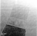
도 11는 본 발명의 바람직한 실시예에 따른 완충 산화막의 증착방법을 통해 형성된 프로파일을 도시한 TEM 사진이다.FIG. 11 is a TEM photograph showing a profile formed by a method of depositing a buffer oxide film according to a preferred embodiment of the present invention. FIG.
도 12는 본 발명의 바람직한 실시예에 따라 형성된 제1 및 제2 폴리실리콘막의 프로파일을 도시한 TEM 사진이다.12 is a TEM photograph showing the profile of the first and second polysilicon films formed in accordance with a preferred embodiment of the present invention.
도 13 및 도 14은 종래기술에 따라 형성된 제1 및 제2 폴리실리콘막의 프로파일을 도시한 TEM 사진이다.13 and 14 are TEM photographs showing profiles of first and second polysilicon films formed according to the prior art.
〈도면의 주요 부분에 대한 부호의 설명〉<Explanation of symbols for main parts of drawing>
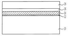
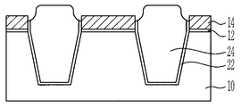
10 : 반도체 기판 12 : 터널 산화막10
14 : 제1 폴리실리콘막 16 : 완충 산화막14
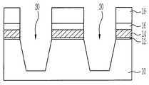
18 : 패드 질화막 20 : 트렌치18: pad nitride film 20: trench
22 : 월 산화막 24 : HDP 산화막22: month oxide film 24: HDP oxide film
26 : 제2 폴리실리콘막26: second polysilicon film
본 발명은 플래시 메모리 소자의 플로팅 게이트 형성방법에 관한 것으로, 특히 후속 월 산화공정시 제1 폴리실리콘막으로 인한 완충 산화막의 두께 증가를 방지하고, 패드 질화막 스트립 공정시 제1 폴리실리콘막으로 가해지는 공격을 최소화할 수 있는 플로팅 게이트 형성방법에 관한 것이다.The present invention relates to a method of forming a floating gate of a flash memory device, and in particular, prevents an increase in the thickness of a buffer oxide film due to a first polysilicon film during a subsequent wall oxidation process, and is applied to the first polysilicon film during a pad nitride film strip process. It relates to a floating gate forming method that can minimize the attack.
최근, 고집적화되는 난드(NAND) 플래시(flash) 메모리 소자를 구현함에 있어서 소자 분리공정으로 SA-STI(Self Aligned Shallow Trench Isolation) 공정이 이용되고 있다. 이에 따라, 플로팅 게이트(floating gate)가 제1 및 제2 폴리실리콘막의 적층구조로 분할되어 형성되고 있다. 이때, 패드 질화막(pad nitride)과 제1 폴리실리콘막 간의 스트레스(stress) 완화를 목적으로 제1 폴리실리콘막과 패드 질화막 증착전에 완충 산화막(buffer oxide)이 적정 두께로 증착된다. 이러한 완충 산화막은 패드 질화막과 제1 폴리실리콘막 간의 스트레스를 완화시키고, 패드 질화막 스트립 공정(strip)시에 제1 폴리실리콘막에 손상이 가해지는 것을 방지하기 위한 베리어(barrier)막으로 사용된다. 이후, 제2 폴리실리콘막의 전처리 세정공정시 에 완충 산화막은 제거되고, HDP(High Density Plasma) 산화막을 증착 및 식각하여 완만한 프로파일(profile)이 형성된다. 그러나, 도 13에 도시된 바와 같이 후속 월 산화공정(wall oxidation) 진행시 제1 폴리실리콘막이 산화되고, 이로 인하여, 완충 산화막의 두께가 증가하게 된다. 이에 따라, 도 14에 도시된 바와 같이 제1 및 제2 폴리실리콘막 계면(interface)에 완충 산화막이 잔류하게 되고, 잔류되는 완충 산화막은 제2 폴리실리콘막의 전처리 세정공정시 완벽하게 제거되지 않아 과도한 HF 딥 타임(dip time)이 요구되게 된다. 또한 제1 폴리실리콘막의 산화로 인하여 제1 폴리실리콘막의 실제 두께가 증착시보다 10% 내지 20% 정도 줄어들게 된다. 제1 폴리실리콘막의 산화는 아이솔레이션(isolation)의 임계치수(Critical Demension)의 크기에 따라 월 산화공정에 의한 산화정도 차이가 다르게 발생되므로, 이때 증가한 두께 역시 달라 웨이퍼(wafer) 전면에 걸쳐 균일한 완충 산화막을 남길수 없게 된다.Recently, in implementing a highly integrated NAND flash memory device, a self-aligned shallow trench isolation (SA-STI) process has been used as a device isolation process. Accordingly, a floating gate is formed by dividing the first and second polysilicon films into a stacked structure. In this case, for the purpose of alleviating stress between the pad nitride film and the first polysilicon film, a buffer oxide film is deposited to an appropriate thickness before deposition of the first polysilicon film and the pad nitride film. The buffer oxide film is used as a barrier film to relieve stress between the pad nitride film and the first polysilicon film and to prevent damage to the first polysilicon film during the pad nitride film stripping process. Subsequently, during the pretreatment cleaning process of the second polysilicon film, the buffer oxide film is removed, and the HDP (High Density Plasma) oxide film is deposited and etched to form a gentle profile. However, as shown in FIG. 13, during the subsequent wall oxidation, the first polysilicon film is oxidized, thereby increasing the thickness of the buffer oxide film. Accordingly, as shown in FIG. 14, the buffer oxide film remains at the first and second polysilicon film interfaces, and the remaining buffer oxide film is not completely removed during the pretreatment cleaning process of the second polysilicon film. HF deep time is required. In addition, due to the oxidation of the first polysilicon film, the actual thickness of the first polysilicon film is reduced by about 10% to 20% than that during deposition. Oxidation of the first polysilicon film is different in the degree of oxidation due to the monthly oxidation process according to the size of the critical dimension of the isolation (isolation), so the increased thickness is also different, uniform buffering across the entire wafer (wafer) You will not be able to leave oxides.
따라서, 본 발명의 바람직한 실시예는 완충 산화막의 증착에 따른 후속 월 산화공정시 제1 폴리실리콘막으로 인한 완충 산화막의 두께 증가를 방지하고, 패드 질화막 스트립 공정시 제1 폴리실리콘막으로 가해지는 공격을 최소화하는데 그 목적이 있다.
Therefore, a preferred embodiment of the present invention prevents the increase in the thickness of the buffer oxide film due to the first polysilicon film during the subsequent wall oxidation process following the deposition of the buffer oxide film, and the attack applied to the first polysilicon film during the pad nitride film strip process. The goal is to minimize this.
본 발명의 일측면에 따르면, 터널 산화막 및 제1 폴리실리콘막이 형성된 반도체 기판이 제공되는 단계와, 상기 제1 폴리실리콘막 상에 완충 산화막 및 패드 질화막이 순차적으로 형성되는 단계와, 상기 반도체 기판 내에 트렌치가 형성되는 단계와, 상기 트렌치가 매립되도록 소자 분리막용 산화막이 증착된 후 상기 패드 질화막을 베리어로 이용한 평탄화 공정이 실시되는 단계와, 상기 패드 질화막이 제거되는 동시에 상기 완충 산화막이 적어도 50% 정도 제거되도록 스트립 공정이 실시되는 단계와, 전처리 세정공정을 통해 상기 완충 산화막이 제거되는 단계와, 전체 구조 상부에 제2 폴리실리콘막이 증착된 후 패터닝공정을 통해 패터닝되어 제1 및 제2 폴리실리콘막으로 이루어진 플로팅 게이트가 형성되는 단계를 포함하는 플로팅 게이트 형성방법이 제공된다.According to an aspect of the present invention, there is provided a semiconductor substrate having a tunnel oxide film and a first polysilicon film formed thereon, and sequentially forming a buffer oxide film and a pad nitride film on the first polysilicon film; Forming a trench, depositing an oxide film for device isolation so that the trench is buried, and then performing a planarization process using the pad nitride as a barrier, and removing the pad nitride and at least 50% of the buffer oxide. Removing the buffer oxide film through a pretreatment cleaning process, depositing a second polysilicon film on the entire structure, and then patterning the patterned first and second polysilicon films by a patterning process. Floating gate forming method comprising the step of forming a floating gate consisting of Is provided.
이하, 첨부된 도면을 참조하여 본 발명의 바람직한 실시예를 설명하기로 한다. 그러나, 본 발명은 이하에서 개시되는 실시예에 한정되는 것이 아니라 서로 다른 다양한 형태로 구현될 수 있으며, 단지 본 실시예는 본 발명의 개시가 완전하도록하며 통상의 지식을 가진자에게 발명의 범주를 완전하게 알려주기 위해 제공되는 것이다.Hereinafter, with reference to the accompanying drawings will be described a preferred embodiment of the present invention. However, the present invention is not limited to the embodiments disclosed below, but may be implemented in various forms, and only the present embodiments are intended to complete the disclosure of the present invention and to those skilled in the art. It is provided for complete information.
도 1 내지 도 9는 본 발명의 바람직한 실시예에 따른 플래시 메모리 소자의 플로팅 게이트 형성방법을 설명하기 위하여 도시한 단면도들이다. 여기서, 도 1 내지 도 9에 도시된 참조부호들 중 서로 동일한 참조부호는 동일한 기능을 하는 동일한 구성요소이다.1 to 9 are cross-sectional views illustrating a method of forming a floating gate of a flash memory device according to an exemplary embodiment of the present invention. Here, the same reference numerals among the reference numerals shown in FIGS. 1 to 9 are the same components having the same function.
도 1을 참조하면, 전처리 세정공정에 의해 세정된 반도체 기판(10)이 제공된 다. 상기 전처리 세정공정은 DHF(Diluted HF)로 세정한 후 SC-1(NH4OH/H2O2/H2O)로 실시되거나, BOE(Buffer Oxide Etchant)로 세정한 후 SC-1로 순차적으로 실시될 수 있다. 상기 전처리 세정공정후, 웰(well; 미도시) 형성용 이온주입공정과 문턱전압 조절용 이온주입공정이 실시된다. 이때, 상기 이온주입공정들은 희생 산화막(sacrificial oxide; 미도시)을 스크린 산화막(screen oxide)으로 이용하여 실시된다. 이로써, 반도체 기판(10)에는 웰 영역이 형성된다. 상기 이온주입공정들이 완료된 후, 반도체 기판(10) 상에는 터널 산화막(12)이 형성된다. 한편, 도시되진 않았지만, 고전압 트랜지스터가 형성될 영역에는 고전압 게이트 산화막(high voltage gate oxide; 미도시)이 형성될 수 있다.Referring to FIG. 1, a
상기 터널 산화막(12)이 형성된 후, 상기 터널 산화막(12) 상에는 제1 폴리실리콘막(14)이 증착된다. 이때, 제1 폴리실리콘막(14)은 LP-CVD(Low Pressure Chemical Vapor Deposition) 방식으로 언도프트(undoped) 비정질 실리콘막으로 300Å 내지 500Å의 두께로 증착된다. 상기 LP-CVD 방식은 480℃ 내지 550℃의 온도범위내에서 SiH4 가스를 소오스 가스로 하여 0.1torr 내지 1torr의 압력범위내에서 실시된다.After the
상기 제1 폴리실리콘막(14)이 형성된 후, 상기 제1 폴리실리콘막(14) 상에는 완충 산화막(16)이 형성된다. 상기 완충 산화막(16)은 HTO(High Temperature Oxide), TEOS(Tetra Ethyle Ortho Silicate), DCS-HTO(DiChloroSilane(SiH2Cl2)-HTO) 등의 산화막 계열을 선택적으로 이용하여 형성된다. 또한, 상기 완충 산화막(16)은 50Å 미만의 두께로 증착되는 것이 바람직하다. 이는, 도 4에서 실시되는 후속 월 산화공정에 의해 상기 제1 폴리실리콘막(14)이 산화되고, 이로 인한, 제1 폴리실리콘막(14)의 두께 감소를 억제하며, 완충 산화막(16)의 불균일한 두께 증가를 제어하기 위함이다. 이러한 결과는 도 10 및 도 11에 도시된 TEM 사진을 통해서도 확인할 수 있다. 도 10은 종래기술에 따른 증착방식으로 완충 산화막(16)을 증착하는 경우의 프로파일이고, 도 11은 본 발명의 바람직한 실시예에서와 같이 완충 산화막(16)을 50Å 미만, 예컨대 30Å 내지 50Å으로 그 두께를 제어하는 경우의 프로파일이다. 도 11에 도시된 바와 같이 본 발명의 바람직한 실시예의 경우에는 제1 폴리실리콘막(14)의 산화 정도가 덜하고, 이에 따라 완충 산화막(16)의 두께 증가도 5Å 미만으로 상당히 양호한 프로파일을 보여주고 있다. 도 12와 같이, 제 2 폴리실리콘막(26; 도 8참조) 증착후 계면에 완충 산화막(16)이 잔류되지 않는 완전한 플로팅 게이트를 확보하게 된다.After the
도 2를 참조하면, 도 1에서 상기 완충 산화막(16)이 형성된 후, 상기 완충 산화막(16) 상에는 패드 질화막(18)이 형성된다. 이때, 상기 패드 질화막(18)은 LP-CVD 방식으로 증착된다.Referring to FIG. 2, after the
도 3을 참조하면, 도 2에서 패드 질화막(18)이 형성된 후, 반도체 기판(10) 상에는 포토레지스트(photoresist)가 도포되고, 포토 마스크(photo mask)를 이용한 노광공정 및 현상공정에 의해 소자 분리마스크(미도시)가 형성된다. 이후, 상기 소자 분리마스크를 이용한 식각공정을 실시하여 패드 질화막(18), 완충 산화막(16), 제1 폴리실리콘막(14), 터널 산화막(12) 및 반도체 기판(10)이 순차적으로 패터닝 된다. 이로써, 반도체 기판(10) 내에는 STI 구조의 트렌치(20)가 형성되고, 이에 따라, 필드영역(field)과 활성영역(active)이 정의된다. 이후, 상기 소자 분리마스크는 스트립 공정(strip)을 통해 제거된다.Referring to FIG. 3, after the
도 4를 참조하면, 도 3에서 트렌치(20)가 형성된 후, 노출되는 상기 트렌치(20)의 내부면과, 터널 산화막(12), 제1 폴리실리콘막(14) 및 완충 산화막(16)의 내측벽에는 월 산화막(wall oxide; 22)이 형성된다. 상기 월 산화막(22)은 제1 폴리실리콘막(14)의 재결정화를 방지하기 위함이다. 또한, 월 산화막(22)은 트렌치(20) 형성공정시 트렌치(20)의 측벽의 식각 손상을 보상하고, 트렌치(20)의 상부/저부 모서리 부위의 라운딩(rounding) 처리와 활성영역의 임계치수(Critical Demension)를 감소시키기 위함이다. 이때, 월 산화막(22)은 건식산화방식으로, 800℃ 내지 1000℃의 온도범위내에서 형성되며, 모니터링 웨이퍼 타겟(monitoring wafer target) 기준으로 30Å 내지 100Å의 두께로 형성된다. 이로써, 제1 폴리실리콘막(14)의 산화로 인한 완충 산화막(16)의 두께 증가를 억제할 수 있다. 월 산화막(22)이 형성된 후, 상기 트렌치(20) 내부에는 보이드(void)가 발생되지 않도록 소자 분리막용 HDP(High Density Plasma) 산화막(24)이 갭 필링(gap filling)된다. 이때, HDP 산화막(24)은 4000Å 내지 10000Å 정도의 두께로 증착된다.Referring to FIG. 4, after the
도 5를 참조하면, 도 4에서 HDP 산화막(24)이 갭 필링된 후, 패드 질화막(18)을 베리어(barrier)로 이용한 CMP 공정을 통해 전체 구조 상부는 평탄화된다.Referring to FIG. 5, after the
도 6을 참조하면, 도 5에서 평탄화공정이 실시된 후, 패드 질화막(18)을 제거하기 위한 스트립 공정(strip)이 실시된다. 상기 스트립 공정은 인산(H3PO4)을 이용하여 실시되되, 완충 산화막(16)이 적어도 50% 제거되도록 하여 후속 전처리 세정공정시 HF 딥 타임(dip time)을 최소화하여 제1 폴리실리콘막(14)으로의 공격이 방지되도록 한다.Referring to FIG. 6, after the planarization process is performed in FIG. 5, a strip process for removing the
도 7을 참조하면, 이후,전처리 세정공정이 실시되는데, 상기 전처리 세정공정은 SC-1(NH4OH/H2O2/H2O)로 세정한 후 DHF(Diluted HF; HF:H2O이 1:50)로 실시되는 것이 바람직하다. 상기 전처리 세정공정을 통해 완충 산화막(16)이 완전히 제거되는 한편, HDP 산화막(24)의 일부가 제거되고, 이로 인하여, 제1 폴리실리콘막(14)과 제2 폴리실리콘막(26; 도 8에서 형성됨) 사이의 계면에 잔류되는 완충 산화막(16)이 모두 제거되면서 전체 상부면에 대해서 완만한 프로파일(profile)을 얻을 수 있다. 이러한 결과는 도 12에 도시된 TEM 사진을 통해서도 확인할 수 있다.Referring to FIG. 7, a pretreatment cleaning process is performed. The pretreatment cleaning process is performed by washing with SC-1 (NH4 OH / H2 O2 / H2 O), followed by DHF (Diluted HF; HF: H2). It is preferred that O is carried out at 1:50). The
도 8을 참조하면, 전체 구조 상부에는 제2 폴리실리콘막(26)이 증착된다. 이때, 제2 폴리실리콘막(26)은 SiH4 가스, 또는 Si2H6 가스와 PH3 가스의 혼합가스를 소오스 가스로 하여 510℃ 내지 550℃ 온도와 0.1Torr 내지 3Torr의 압력범위내에서 LP-CVD(Low Pressure Chemical Vapor Deposition) 방식으로 증착된다. 또한, 제2 폴리실리콘막(26)은 도프트(doped) 폴리실리콘막으로 증착되며, 도핑되는 인 농도는 1.0E20atoms/cc 내지 2.0E20atoms/cc 정도의 도핑 레벨(level)을 부여하여 1000Å 내지 2000Å으로 증착된다.Referring to FIG. 8, a second polysilicon film 26 is deposited on the entire structure. At this time, the second polysilicon film 26 may be a LP gas within a pressure range of 510 ° C. to 550 ° C. and a pressure of 0.1 Torr to 3 Torr using SiH4 gas or a mixed gas of Si2 H6 gas and PH3 gas as a source gas. It is deposited by a low pressure chemical vapor deposition (CVD) method. In addition, the second polysilicon film 26 is deposited as a doped polysilicon film, and the doped phosphorus concentration is about 1000 Pa to 2000 Pa by giving a doping level of about 1.0E20 atoms / cc to 2.0E20 atoms / cc. Is deposited.
도 9를 참조하면, 도 8에서 제2 폴리실리콘막(26)이 증착된 후, 리소그래피(lithography) 공정을 통해 플로팅 게이트가 형성된다. 이때, 플로팅 게이트는 외측벽이 수직 또는 약간의 경사를 갖도록 식각되어 형성된다. 이로써, 인접한 플로팅 게이트(미도시) 과의 스페이스(space)를 확보하는 것이 가능하다.Referring to FIG. 9, after the second polysilicon layer 26 is deposited in FIG. 8, a floating gate is formed through a lithography process. At this time, the floating gate is formed by etching the outer wall to have a vertical or slight inclination. As a result, it is possible to secure a space with an adjacent floating gate (not shown).
상기에서 설명한 본 발명의 기술적 사상은 바람직한 실시예에서 구체적으로 기술되었으나, 상기한 실시예는 그 설명을 위한 것이며 그 제한을 위한 것이 아님을 주의하여야 한다. 또한, 본 발명은 본 발명의 기술 분야의 통상의 전문가라면 본 발명의 기술적 사상의 범위 내에서 다양한 실시예가 가능함을 이해할 수 있을 것이다.Although the technical spirit of the present invention described above has been described in detail in a preferred embodiment, it should be noted that the above-described embodiment is for the purpose of description and not of limitation. In addition, the present invention will be understood by those skilled in the art that various embodiments are possible within the scope of the technical idea of the present invention.
상술한 바와 같이, 본 발명에 의하면, 제1 폴리실리콘막과 패드 질화막 사이에 두께를 최소화하여 완충 산화막을 형성함으로써 제1 폴리실리콘막의 추가 산화를 방지하고, 이로 인하여 완충 산화막의 균일한 제거가 가능하며, 상기 패드 질화막의 스트립 공정시 사용되는 용액(H3PO4)이 상기 제1 폴리실리콘막을 공격하는 것을 방지할 수 있다. 이에 따라, 반도체 소자의 특성을 향상시킬 수 있다.As described above, according to the present invention, by minimizing the thickness between the first polysilicon film and the pad nitride film to form a buffer oxide film, further oxidation of the first polysilicon film is prevented, thereby allowing uniform removal of the buffer oxide film. The solution (H3 PO4 ) used in the strip process of the pad nitride layer may prevent the first polysilicon layer from attacking. Thereby, the characteristic of a semiconductor element can be improved.
또한, 본 발명에 의하면, 제1 폴리실리콘막과 패드 질화막 사이에 완충 산화 막을 형성하여 상기 제1 폴리실리콘막과 상기 패드 질화막이 직접적으로 접촉되는 것을 방지함으로써 이 들막의 접촉에 의해 생기는 스트레스(stress)를 완화하여 하부층인 터널 산화막의 열화를 방지할 수 있다.In addition, according to the present invention, a stress caused by the contact of these fields is formed by forming a buffer oxide film between the first polysilicon film and the pad nitride film to prevent direct contact between the first polysilicon film and the pad nitride film. ) Can be prevented from deteriorating the tunnel oxide film as the lower layer.
또한, 본 발명에 의하면, 상기 공정을 통해 제2 폴리실리콘막의 증착후에 최종적인 플로팅 게이트의 표면 거칠기(roughness)를 완화하여 후속 공정을 통해 형성되는 유전체막의 특성을 향상시킬 수 있다.In addition, according to the present invention, after the deposition of the second polysilicon film, the surface roughness of the final floating gate may be alleviated to improve the characteristics of the dielectric film formed through the subsequent process.
또한, 본 발명에 의하면, 제2 폴리실리콘막 증착공정전에 실시되는 전처리 세정공정을 통한 완충 산화막 제거시에 HDP 산화막의 측벽/모서리를 상당량 제거할 수 있어서 HDP 산화막의 튀어 나온 부분이 완화되어 완만한 프로파일 형성이 가능하다.In addition, according to the present invention, a considerable amount of sidewalls / edges of the HDP oxide film can be removed at the time of removing the buffer oxide film through the pretreatment cleaning step performed before the second polysilicon film deposition step, so that the protruding portion of the HDP oxide film is alleviated to be gentle. Profile formation is possible.
또한, 본 발명에 의하면, SA-STI(Self Aligned Shallow Trench Isolation) 공정의 적용에 따라 월 산화공정에 의해 트렌치 모서리(corner)에 원하는 두께 보다 작게 증착되는 게이트 산화막 얇아짐 현상을 방지할 수 있다. 또한, 임계치수(Critical Demension) 만큼의 활성영역을 확보할 수 있어 소자의 리텐션 패일(fail)이나 빠른 소거 동작 등의 전기적인 특성이 개선되어 신뢰성을 확보할 수 있다.In addition, according to the present invention, the gate oxide film thinning may be prevented from being deposited at a trench corner smaller than a desired thickness by a monthly oxidation process according to the application of a self aligned shallow trench isolation (SA-STI) process. In addition, since an active area corresponding to a critical dimension can be secured, electrical characteristics such as retention failure and fast erase of the device can be improved, thereby ensuring reliability.
또한, 본 발명에 의하면, 노출되는 터널 산화막을 보호하도록 월 산화막을 형성하여 터널 산화막의 공격을 방지함으로써 채널 폭(channel width) 내에서의 균일한 터널 산화막을 형성할 수 있다.In addition, according to the present invention, a wall oxide film is formed to protect the exposed tunnel oxide film to prevent attack of the tunnel oxide film, thereby forming a uniform tunnel oxide film within a channel width.
또한, 본 발명에 의하면, 복잡한 공정 및 장비의 추가 소요없이 기존의 장비 와 공정을 이용하여 낮은 비용(low cost)와 높은 신뢰성(high reliability)를 가지는 반도체 소자를 형성할 수 있다.In addition, according to the present invention, a semiconductor device having low cost and high reliability can be formed using existing equipment and processes without the need for complicated process and additional equipment.
Claims (5)
Translated fromKoreanPriority Applications (4)
| Application Number | Priority Date | Filing Date | Title |
|---|---|---|---|
| KR1020030043619AKR100578656B1 (en) | 2003-06-30 | 2003-06-30 | Floating gate formation method of flash memory device |
| JP2003390732AJP4371361B2 (en) | 2003-06-30 | 2003-11-20 | Floating gate forming method for flash memory device |
| US10/720,408US6964913B2 (en) | 2003-06-30 | 2003-11-24 | Method for forming floating gate in flash memory device |
| TW092133187ATWI249816B (en) | 2003-06-30 | 2003-11-26 | Method for forming floating gate in flash memory device |
Applications Claiming Priority (1)
| Application Number | Priority Date | Filing Date | Title |
|---|---|---|---|
| KR1020030043619AKR100578656B1 (en) | 2003-06-30 | 2003-06-30 | Floating gate formation method of flash memory device |
Publications (2)
| Publication Number | Publication Date |
|---|---|
| KR20050002250A KR20050002250A (en) | 2005-01-07 |
| KR100578656B1true KR100578656B1 (en) | 2006-05-11 |
Family
ID=33536397
Family Applications (1)
| Application Number | Title | Priority Date | Filing Date |
|---|---|---|---|
| KR1020030043619AExpired - Fee RelatedKR100578656B1 (en) | 2003-06-30 | 2003-06-30 | Floating gate formation method of flash memory device |
Country Status (4)
| Country | Link |
|---|---|
| US (1) | US6964913B2 (en) |
| JP (1) | JP4371361B2 (en) |
| KR (1) | KR100578656B1 (en) |
| TW (1) | TWI249816B (en) |
Families Citing this family (22)
| Publication number | Priority date | Publication date | Assignee | Title |
|---|---|---|---|---|
| ITMI20031591A1 (en)* | 2003-08-01 | 2005-02-02 | St Microelectronics Srl | METHOD FOR MANUFACTURING INSULATION STRUCTURES |
| KR100487657B1 (en)* | 2003-08-13 | 2005-05-03 | 삼성전자주식회사 | mos transistor with recessed gate and method of fabricating the same |
| US7067377B1 (en)* | 2004-03-30 | 2006-06-27 | Fasl Llc | Recessed channel with separated ONO memory device |
| US7482223B2 (en)* | 2004-12-22 | 2009-01-27 | Sandisk Corporation | Multi-thickness dielectric for semiconductor memory |
| US7202125B2 (en)* | 2004-12-22 | 2007-04-10 | Sandisk Corporation | Low-voltage, multiple thin-gate oxide and low-resistance gate electrode |
| KR100680488B1 (en)* | 2005-01-13 | 2007-02-08 | 주식회사 하이닉스반도체 | Manufacturing Method of Flash Memory Device |
| KR100784083B1 (en)* | 2005-06-13 | 2007-12-10 | 주식회사 하이닉스반도체 | Floating gate formation method of flash memory device |
| KR100650813B1 (en)* | 2005-06-30 | 2006-11-27 | 주식회사 하이닉스반도체 | Flash memory devices |
| KR100650857B1 (en)* | 2005-12-23 | 2006-11-28 | 주식회사 하이닉스반도체 | Manufacturing Method of Flash Memory Device |
| KR100745957B1 (en)* | 2006-02-07 | 2007-08-02 | 주식회사 하이닉스반도체 | Manufacturing Method of Flash Memory Device |
| KR100777016B1 (en)* | 2006-06-20 | 2007-11-16 | 재단법인서울대학교산학협력재단 | NAND flash memory array with columnar structure and manufacturing method |
| KR100994891B1 (en)* | 2007-02-26 | 2010-11-16 | 주식회사 하이닉스반도체 | Device Separation Method of Semiconductor Memory Device |
| KR20080084166A (en)* | 2007-03-15 | 2008-09-19 | 주식회사 하이닉스반도체 | Device Separation Method of Semiconductor Memory Device |
| KR20080099463A (en)* | 2007-05-09 | 2008-11-13 | 주식회사 하이닉스반도체 | Semiconductor device, nonvolatile memory device and manufacturing method thereof |
| KR100953064B1 (en)* | 2007-06-28 | 2010-04-13 | 주식회사 하이닉스반도체 | Manufacturing method of nonvolatile memory device |
| US8115254B2 (en) | 2007-09-25 | 2012-02-14 | International Business Machines Corporation | Semiconductor-on-insulator structures including a trench containing an insulator stressor plug and method of fabricating same |
| US8492846B2 (en) | 2007-11-15 | 2013-07-23 | International Business Machines Corporation | Stress-generating shallow trench isolation structure having dual composition |
| KR101098113B1 (en)* | 2010-07-07 | 2011-12-26 | 주식회사 하이닉스반도체 | Method of forming a semiconductor device |
| CN104979354B (en)* | 2014-04-01 | 2018-02-09 | 北京兆易创新科技股份有限公司 | A kind of structure of ETOX NOR-types flash memory and preparation method thereof |
| TWI556321B (en)* | 2014-04-23 | 2016-11-01 | 穩懋半導體股份有限公司 | Process for implanting boron isolation structure with high electron mobility transistor |
| CN107799528B (en)* | 2016-08-30 | 2020-07-17 | 华邦电子股份有限公司 | Method for manufacturing memory element |
| CN114743979A (en)* | 2022-03-28 | 2022-07-12 | 上海华虹宏力半导体制造有限公司 | A kind of preparation method of semiconductor structure |
Family Cites Families (4)
| Publication number | Priority date | Publication date | Assignee | Title |
|---|---|---|---|---|
| US6326283B1 (en)* | 2000-03-07 | 2001-12-04 | Vlsi Technology, Inc. | Trench-diffusion corner rounding in a shallow-trench (STI) process |
| KR100339890B1 (en)* | 2000-08-02 | 2002-06-10 | 윤종용 | Method for Self-Aligned Shallow Trench Isolation and Method of manufacturing Non-Volatile Memory Device comprising the same |
| US6620681B1 (en)* | 2000-09-08 | 2003-09-16 | Samsung Electronics Co., Ltd. | Semiconductor device having desired gate profile and method of making the same |
| US6559008B2 (en)* | 2001-10-04 | 2003-05-06 | Hynix Semiconductor America, Inc. | Non-volatile memory cells with selectively formed floating gate |
- 2003
- 2003-06-30KRKR1020030043619Apatent/KR100578656B1/ennot_activeExpired - Fee Related
- 2003-11-20JPJP2003390732Apatent/JP4371361B2/ennot_activeExpired - Fee Related
- 2003-11-24USUS10/720,408patent/US6964913B2/ennot_activeExpired - Fee Related
- 2003-11-26TWTW092133187Apatent/TWI249816B/ennot_activeIP Right Cessation
Also Published As
| Publication number | Publication date |
|---|---|
| JP4371361B2 (en) | 2009-11-25 |
| TW200501335A (en) | 2005-01-01 |
| TWI249816B (en) | 2006-02-21 |
| JP2005026647A (en) | 2005-01-27 |
| KR20050002250A (en) | 2005-01-07 |
| US20040266135A1 (en) | 2004-12-30 |
| US6964913B2 (en) | 2005-11-15 |
Similar Documents
| Publication | Publication Date | Title |
|---|---|---|
| KR100578656B1 (en) | Floating gate formation method of flash memory device | |
| KR100473733B1 (en) | Semiconductor device and method for manufacturing the same | |
| US7037785B2 (en) | Method of manufacturing flash memory device | |
| US20080020544A1 (en) | Method for Forming Wall Oxide Layer and Isolation Layer in Flash Memory Device | |
| US20070232019A1 (en) | Method for forming isolation structure in nonvolatile memory device | |
| US7052960B2 (en) | Method for manufacturing a flash memory device | |
| US20040014269A1 (en) | Method of manufacturing flash memory device | |
| KR100875067B1 (en) | Manufacturing Method of Flash Memory Device | |
| KR20060025295A (en) | Gate electrode formation method of nonvolatile memory device | |
| KR20070118348A (en) | Manufacturing method of nonvolatile memory device | |
| KR100575343B1 (en) | Manufacturing Method of Flash Memory Device | |
| US7521320B2 (en) | Flash memory device and method of manufacturing the same | |
| KR100554835B1 (en) | Manufacturing Method of Flash Device | |
| KR100673224B1 (en) | Manufacturing Method of Flash Memory Device | |
| KR20040005230A (en) | Method for manufacturing flash memory | |
| KR20050002248A (en) | Method for forming a floating gate in flash memory device | |
| KR100709468B1 (en) | Floating gate formation method of flash memory device | |
| KR100976698B1 (en) | Method of forming gate oxide film of semiconductor device | |
| KR100870303B1 (en) | Manufacturing Method of Flash Memory Device | |
| KR20030094440A (en) | Method of forming a isolation layer in a semiconductor device and manufacturing a flash memory cell using the same | |
| KR100806516B1 (en) | Manufacturing Method of NAND Flash Memory Device | |
| KR20050002085A (en) | Method for forming a floating gate in flash memory device | |
| KR20040054144A (en) | Method for manufacturing a flash memory device | |
| KR20050073311A (en) | Method of manufacturing a flash memory device | |
| KR20050122649A (en) | An isolation layer of flash memory device and a method for forming the isolation layer |
Legal Events
| Date | Code | Title | Description |
|---|---|---|---|
| PA0109 | Patent application | St.27 status event code:A-0-1-A10-A12-nap-PA0109 | |
| A201 | Request for examination | ||
| PA0201 | Request for examination | St.27 status event code:A-1-2-D10-D11-exm-PA0201 | |
| PG1501 | Laying open of application | St.27 status event code:A-1-1-Q10-Q12-nap-PG1501 | |
| D13-X000 | Search requested | St.27 status event code:A-1-2-D10-D13-srh-X000 | |
| D14-X000 | Search report completed | St.27 status event code:A-1-2-D10-D14-srh-X000 | |
| E902 | Notification of reason for refusal | ||
| PE0902 | Notice of grounds for rejection | St.27 status event code:A-1-2-D10-D21-exm-PE0902 | |
| P11-X000 | Amendment of application requested | St.27 status event code:A-2-2-P10-P11-nap-X000 | |
| P13-X000 | Application amended | St.27 status event code:A-2-2-P10-P13-nap-X000 | |
| N231 | Notification of change of applicant | ||
| PN2301 | Change of applicant | St.27 status event code:A-3-3-R10-R13-asn-PN2301 St.27 status event code:A-3-3-R10-R11-asn-PN2301 | |
| E701 | Decision to grant or registration of patent right | ||
| PE0701 | Decision of registration | St.27 status event code:A-1-2-D10-D22-exm-PE0701 | |
| PR1002 | Payment of registration fee | St.27 status event code:A-2-2-U10-U11-oth-PR1002 Fee payment year number:1 | |
| GRNT | Written decision to grant | ||
| PR0701 | Registration of establishment | St.27 status event code:A-2-4-F10-F11-exm-PR0701 | |
| PG1601 | Publication of registration | St.27 status event code:A-4-4-Q10-Q13-nap-PG1601 | |
| PR1001 | Payment of annual fee | St.27 status event code:A-4-4-U10-U11-oth-PR1001 Fee payment year number:4 | |
| PR1001 | Payment of annual fee | St.27 status event code:A-4-4-U10-U11-oth-PR1001 Fee payment year number:5 | |
| PR1001 | Payment of annual fee | St.27 status event code:A-4-4-U10-U11-oth-PR1001 Fee payment year number:6 | |
| PN2301 | Change of applicant | St.27 status event code:A-5-5-R10-R13-asn-PN2301 St.27 status event code:A-5-5-R10-R11-asn-PN2301 | |
| FPAY | Annual fee payment | Payment date:20120424 Year of fee payment:7 | |
| PR1001 | Payment of annual fee | St.27 status event code:A-4-4-U10-U11-oth-PR1001 Fee payment year number:7 | |
| PN2301 | Change of applicant | St.27 status event code:A-5-5-R10-R13-asn-PN2301 St.27 status event code:A-5-5-R10-R11-asn-PN2301 | |
| FPAY | Annual fee payment | Payment date:20130426 Year of fee payment:8 | |
| PR1001 | Payment of annual fee | St.27 status event code:A-4-4-U10-U11-oth-PR1001 Fee payment year number:8 | |
| LAPS | Lapse due to unpaid annual fee | ||
| PC1903 | Unpaid annual fee | St.27 status event code:A-4-4-U10-U13-oth-PC1903 Not in force date:20140504 Payment event data comment text:Termination Category : DEFAULT_OF_REGISTRATION_FEE | |
| PC1903 | Unpaid annual fee | St.27 status event code:N-4-6-H10-H13-oth-PC1903 Ip right cessation event data comment text:Termination Category : DEFAULT_OF_REGISTRATION_FEE Not in force date:20140504 | |
| PN2301 | Change of applicant | St.27 status event code:A-5-5-R10-R13-asn-PN2301 St.27 status event code:A-5-5-R10-R11-asn-PN2301 | |
| P22-X000 | Classification modified | St.27 status event code:A-4-4-P10-P22-nap-X000 |