KR100578233B1 - Data input / output variable control device of synchronous memory device - Google Patents
Data input / output variable control device of synchronous memory deviceDownload PDFInfo
- Publication number
- KR100578233B1 KR100578233B1KR1020000087069AKR20000087069AKR100578233B1KR 100578233 B1KR100578233 B1KR 100578233B1KR 1020000087069 AKR1020000087069 AKR 1020000087069AKR 20000087069 AKR20000087069 AKR 20000087069AKR 100578233 B1KR100578233 B1KR 100578233B1
- Authority
- KR
- South Korea
- Prior art keywords
- prefetch
- input
- output
- bit
- unit
- Prior art date
- Legal status (The legal status is an assumption and is not a legal conclusion. Google has not performed a legal analysis and makes no representation as to the accuracy of the status listed.)
- Expired - Fee Related
Links
Images


Classifications
- G—PHYSICS
- G11—INFORMATION STORAGE
- G11C—STATIC STORES
- G11C11/00—Digital stores characterised by the use of particular electric or magnetic storage elements; Storage elements therefor
- G11C11/21—Digital stores characterised by the use of particular electric or magnetic storage elements; Storage elements therefor using electric elements
- G11C11/34—Digital stores characterised by the use of particular electric or magnetic storage elements; Storage elements therefor using electric elements using semiconductor devices
- G11C11/40—Digital stores characterised by the use of particular electric or magnetic storage elements; Storage elements therefor using electric elements using semiconductor devices using transistors
- G11C11/401—Digital stores characterised by the use of particular electric or magnetic storage elements; Storage elements therefor using electric elements using semiconductor devices using transistors forming cells needing refreshing or charge regeneration, i.e. dynamic cells
- G11C11/4063—Auxiliary circuits, e.g. for addressing, decoding, driving, writing, sensing or timing
- G11C11/407—Auxiliary circuits, e.g. for addressing, decoding, driving, writing, sensing or timing for memory cells of the field-effect type
- G11C11/409—Read-write [R-W] circuits
- G11C11/4096—Input/output [I/O] data management or control circuits, e.g. reading or writing circuits, I/O drivers or bit-line switches
- G—PHYSICS
- G11—INFORMATION STORAGE
- G11C—STATIC STORES
- G11C7/00—Arrangements for writing information into, or reading information out from, a digital store
- G11C7/10—Input/output [I/O] data interface arrangements, e.g. I/O data control circuits, I/O data buffers
- G11C7/1051—Data output circuits, e.g. read-out amplifiers, data output buffers, data output registers, data output level conversion circuits
- G11C7/106—Data output latches
- G—PHYSICS
- G11—INFORMATION STORAGE
- G11C—STATIC STORES
- G11C7/00—Arrangements for writing information into, or reading information out from, a digital store
- G11C7/10—Input/output [I/O] data interface arrangements, e.g. I/O data control circuits, I/O data buffers
- G11C7/1051—Data output circuits, e.g. read-out amplifiers, data output buffers, data output registers, data output level conversion circuits
- G—PHYSICS
- G11—INFORMATION STORAGE
- G11C—STATIC STORES
- G11C7/00—Arrangements for writing information into, or reading information out from, a digital store
- G11C7/10—Input/output [I/O] data interface arrangements, e.g. I/O data control circuits, I/O data buffers
- G11C7/1072—Input/output [I/O] data interface arrangements, e.g. I/O data control circuits, I/O data buffers for memories with random access ports synchronised on clock signal pulse trains, e.g. synchronous memories, self timed memories
- G—PHYSICS
- G11—INFORMATION STORAGE
- G11C—STATIC STORES
- G11C7/00—Arrangements for writing information into, or reading information out from, a digital store
- G11C7/10—Input/output [I/O] data interface arrangements, e.g. I/O data control circuits, I/O data buffers
- G11C7/1078—Data input circuits, e.g. write amplifiers, data input buffers, data input registers, data input level conversion circuits
- G11C7/1087—Data input latches
- G—PHYSICS
- G11—INFORMATION STORAGE
- G11C—STATIC STORES
- G11C2207/00—Indexing scheme relating to arrangements for writing information into, or reading information out from, a digital store
- G11C2207/10—Aspects relating to interfaces of memory device to external buses
- G11C2207/107—Serial-parallel conversion of data or prefetch
Landscapes
- Engineering & Computer Science (AREA)
- Databases & Information Systems (AREA)
- Microelectronics & Electronic Packaging (AREA)
- Computer Hardware Design (AREA)
- Dram (AREA)
Abstract
Translated fromKoreanDescription
Translated fromKorean도1은 메모리 입출력단의 프리페치 유닛이 3종류로 되어 있는 구성예시도이고,Fig. 1 is an exemplary configuration diagram in which three types of prefetch units of a memory input / output stage are used.
도 2는 메모리 입출력단의 프리페치 유닛이 단일의 4비트 프리페치로 된 구성예시도이고,2 is an exemplary configuration diagram in which the prefetch unit of the memory input / output stage is a single 4-bit prefetch,
도 3은 도 2의 4비트 프리페치를 3가지 방법으로 선택하기 위한 구성예시도이다.3 is an exemplary configuration diagram for selecting the 4-bit prefetch of FIG. 2 in three ways.
본 발명은 SDRAM의 데이터 입출력 가변제어장치에 관한 것이다.The present invention relates to a data input / output variable control device of an SDRAM.
종래의 메모리는 데이터를 입출력하는 방식인 프리페치방식이 고정적이어서 1비트 프리페치 방식으로 생산된 SDRAM은 2비트 프리페치 방식을 사용하는 DDR SDRAM이 될 수가 없고, 역으로 2비트 프리페치 방식으로 생산된 DDR SDRAM은 1비트 프리페치 방식을 사용하는 DDR SDRAM을 대체할 수 없기 때문에 메모리의 활용도가 낮고 자원의 낭비도 커지는 문제점이 존재하였다.Conventional memory has a fixed prefetch method for inputting / outputting data, and thus SDRAM produced by a 1-bit prefetch method cannot be a DDR SDRAM using a 2-bit prefetch method, and conversely, a 2-bit prefetch method. Since DDR SDRAM cannot replace DDR SDRAM using 1-bit prefetch, there is a problem of low memory utilization and large waste of resources.
이와 같은 문제점을 해결하기 위하여 본 발명에서는 메모리의 프리페치방식을 자유롭게 변화시킴으로써 메모리의 활용도를 향상시킨 동기식메모리장치의 데이터 입출력 가변제어장치를 제공함을 목적으로 한다.In order to solve the above problems, an object of the present invention is to provide a data input / output variable control device of a synchronous memory device which improves the utilization of the memory by freely changing the prefetch method of the memory.
본 발명의 다른 목적은 외부 명령을 이용하여 정보를 레지스터에 저장하는 방법을 사용함으로써 메모리의 프리페치방식을 변화시켜 메모리의 활용도를 향상시킨 동기식메모리장치의 데이터 입출력 가변제어장치를 제공함에 있다.Another object of the present invention is to provide a data input / output variable control device of a synchronous memory device which improves the utilization of the memory by changing the prefetch method of the memory by using a method of storing information in a register using an external command.
본 발명의 또 다른 목적은 본딩 옵션을 사용함으로써 메모리의 프리페치방식을 변화시켜 메모리의 활용도를 향상시킨 동기식메모리장치의 데이터 입출력 가변제어장치를 제공함에 있다.It is still another object of the present invention to provide a data input / output variable control device of a synchronous memory device which improves the utilization of the memory by changing the prefetch method of the memory by using a bonding option.
상기 목적을 달성하기 위한 본 발명의 일 측면에 따르면, 입력 버퍼로부터 전달된 데이터를 프리페치하기 위한 다수의 입력 프리페치 유닛 - 각 입력 프리페치 유닛은 서로 다른 프리페치 단위를 가짐 - ; 메모리 코어로부터 전달된 데이터를 프리페치하기 위한 다수의 출력 프리페치 유닛 - 각 출력 프리페치 유닛은 서로 다른 프리페치 단위를 가짐 - ; 및 커맨드 신호에 응답하여 상기 다수의 입력 프리페치 수단 중 어느 하나와 상기 다수의 출력 프리페치 수단 중 어느 하나를 선택하는 제어신호를 생성하기 위한 제어신호 생성수단을 구비하는 동기식메모리장치의 데이터 입출력 가변제어장치가 제공된다.According to an aspect of the present invention for achieving the above object, a plurality of input prefetch units for prefetching data transferred from an input buffer, each input prefetch unit having a different prefetch unit; Multiple output prefetch units for prefetching data delivered from the memory core, each output prefetch unit having a different prefetch unit; And control signal generation means for generating a control signal for selecting any one of the plurality of input prefetch means and the plurality of output prefetch means in response to a command signal. A control device is provided.
삭제delete
또한, 본 발명의 다른 측면에 따르면, 입력 버퍼로부터 전달된 데이터를 프리페치하기 위한 N-비트 입력 프리페치 유닛; 메모리 코어로부터 전달된 데이터를 프리페치하기 위한 N-비트 출력 프리페치 유닛; 및 커맨드 신호에 응답하여 상기 N-비트 입력 프리페치 유닛과 상기 N-비트 출력 프리페치 유닛의 프리페치 비트수 - 1부터 N 사이의 값을 가짐 - 를 선택하기 위한 선택수단을 구비하는 동기식메모리장치의 데이터 입출력 가변제어장치가 제공된다.According to another aspect of the invention, there is also provided an N-bit input prefetch unit for prefetching data transferred from an input buffer; An N-bit output prefetch unit for prefetching data delivered from the memory core; And selection means for selecting a number of prefetch bits, wherein the value has a value between 1 and N, of the N-bit input prefetch unit and the N-bit output prefetch unit in response to a command signal. A data input / output variable control apparatus is provided.
삭제delete
삭제delete
삭제delete
삭제delete
삭제delete
삭제delete
이하에서는 도면을 참조하여 SDRAM의 데이터 입출력 가변제어장치에 대하여 구체적으로 설명한다.Hereinafter, an apparatus for controlling data input / output of an SDRAM will be described in detail with reference to the accompanying drawings.
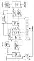
도 1은 메모리 입출력단의 프리페치 유닛이 3종류로 되어 있는 구성예시도이다.Fig. 1 is an exemplary configuration diagram in which there are three types of prefetch units in the memory input / output stage.
커맨드신호(Commands)와 클럭신호(clk, clkb)가 커맨드 디코더부(Command decoder, 105)에 입력되면 상기 커맨드 디코더부(105)에서는 커맨드신호를 클럭신호에 맞춰 뱅크컨트롤부(115), 모드 레지스터부(120) 및 어드레스 버퍼부(110)로 출력한다. 상기 뱅크 컨트롤부(115)에서는 커맨드신호에 맞춰 각 뱅크부(141, 142, 143, 144) 및 로 디코더부(Row decoder, 130)를 제어하며, 상기 모드 레지스터부(120)에서는 메모리를 쓰기 혹은 읽기로 억세스하기 전에, 쓰기 프리페치 유닛(170)과 읽기 프리페치 유닛(150)을 세팅한다. 한편 상기 어드레스 버퍼부(110)에서 출력된 신호는 상기 모드 레지스터부(120), 로 디코더부(130), 컬럼 디코더부(135) 및 컬럼 어드레스 카운터부(125)에 입력된다. 각 뱅크부(141, 142, 143, 144)에서 읽혀진 데이터 신호들은 감지증폭기부(145)에서 증폭되어 미리 선택된 상기 읽기 프리페치 유닛(150)으로 입력되고, 클럭 버퍼부(155)에서 출력된 내부 클럭신호들과 함께 출력 버퍼부(160)에 입력된다. 또한, 내부 클럭신호들은 미리 선택된 상기 쓰기 프리페치 유닛(170)과 입력 버퍼부(165)에 입력되어 상기 입력 버퍼부(165)를 빠져 나온 데이터 신호들이 클럭신호에 맞춰 미리 선택된 상기 쓰기 프리페치 유닛(170)을 통하여 각 뱅크부(140)에 저장되도록 한다.When the command signals Commands and the clock signals clk and clkb are input to the
여기서, 커맨드 셀신호와 어드레스 신호를 입력신호로 하여 각 프리페치 내부에 있는 공지의 논리회로들의 조합으로 3개의 프리페치 유닛 중 하나가 인에이블될 수 있도록 할 수 있다.Here, the command cell signal and the address signal may be used as input signals so that one of the three prefetch units may be enabled by a combination of known logic circuits inside each prefetch.
우선, 1비트 프리페치로 모드 레지스터 값이 세팅되어 있는 경우의 동작은 다음과 같다.First, the operation when the mode register value is set to 1 bit prefetch is as follows.
메모리에 정보를 기록하기 위하여 쓰기(Write)동작을 수행하는 경우, 1비트 프리페치이므로 매 클럭당 한개씩의 데이터가 메모리 셀에 쓰여지고, 메모리의 정보를 출력하기 위하여 읽기(Read)동작을 수행하는 경우에도 매 클럭당 한개씩의 데이터가 출력된다. 즉, 이러한 동작은 일반적인 동기식(Synchronous) DRAM 및 동기식 SRAM에서의 동작과 동일하다.When write operation is performed to write information to memory, one bit prefetch, so one data per clock is written to the memory cell and read operation is performed to output the memory information. One data per clock is output. In other words, this operation is the same as in general synchronous DRAM and synchronous SRAM.
다음으로, 2비트 프리페치로 레지스터의 값이 세팅되어 있는 경우의 동작은 통상적으로 지칭되는 DDR SDRAM과 동일한 동작을 한다. 즉, 외부 클럭의 라이징 에지와 폴링 에지에 각각 하나씩의 데이터를 동시에 정렬하여 쓰기/읽기를 수행하는 방식으로서, 매 클럭당 2개의 데이터가 입출력된다. 이 때, 2비트 프리페치로 동작 을 한다는 것은 직렬적인 2개의 연속하는 데이터를 병렬적인 2개의 단절된 데이터로 변환하거나, 혹은 그 반대의 동작을 수행함을 의미한다. Next, the operation when the value of the register is set to 2-bit prefetch has the same operation as that of the DDR SDRAM which is commonly referred to. That is, as a method of writing and reading data by arranging one data at the same time on the rising edge and the falling edge of the external clock, two data are input and output for each clock. In this case, operating with 2 bits prefetch means converting two consecutive data into two parallel disconnected data, or vice versa.
마지막으로, 4비트 프리페치로 레지스터의 값이 세팅되어 있는 경우에는 데이터가 입출력하는 속도와 내부에서 동작되는 속도가 4배만큼 차이가 나는 것이다. 즉, 즉, 직렬적인 4개의 연속된 데이터를 병렬적인 4개의 단절된 데이터로 변환하거나, 혹은 그 반대의 동작을 수행함을 의미한다. 이러한 동작을 하는 메모리의 예로는 램버스 DRAM과 DDR-II SDRAM 등이 있다.Finally, if the value of the register is set to 4-bit prefetch, the speed at which data is input / output and the speed at which it operates internally differ by four times. That is, it means converting four consecutive data series into four parallel disconnected data, or vice versa. Examples of such memory are Rambus DRAM and DDR-II SDRAM.
도 2는 메모리 입출력단의 프리페치 유닛이 단일의 4비트 프리페치로 된 구성예시도로서, 대부분의 구성요소들은 도 1의 구성요소들과 동일하게 구성 및 작동되고, 메모리 입출력단의 프리페치 유닛만이 단일의 4비트 프리페치로 구비되어 있는 것과 모드 레지스터부에서 상기 4비트 프리페치 구조 중 일정부분을 선택하는 방법만이 다르다.FIG. 2 is an exemplary configuration diagram in which a prefetch unit of a memory input / output stage is a single 4-bit prefetch, and most components are configured and operated in the same manner as the components of FIG. 1, and a prefetch unit of the memory input / output stage is illustrated in FIG. Only the method of selecting a portion of the 4-bit prefetch structure in the mode register section differs from that provided by a single 4-bit prefetch.
여기서, 상기 모드 레지스터부(120)에 의하여 4비트 프리페치 구조의 전부를 선택하면 4비트 프리페치로 동작하고, 4비트 프리페치 구조 중 1/2만을 선택하면 2비트 프리페치로 동작하며, 4비트 프리페치 구조 중 1/4만을 선택하면 1비트 프리페치로 동작하는 것이다.In this case, when the
도 3은 도 2의 4비트 프리페치를 3가지 방법으로 선택하기 위한 구성예시도이다.3 is an exemplary configuration diagram for selecting the 4-bit prefetch of FIG. 2 in three ways.
입력버퍼부(165)에서 출력된 데이터 신호들이 데이터입력래치(310)로 입력되고, 상기 데이터 신호들 가운데 인클럭신호(inclk)에 따라 인에블된 데이터입력래 치(310)에서만 상기 데이터 신호들이 출력되며, 상기 데이터 신호들을 각 뱅크부(140)내 셀 블럭(330)에 입력시키기 위하여 데이터입력래치(310) 후단에 위치하는 입력멀티플렉서(320)는 모드 레지스터부(120)에서 출력되는 어드레스신호(Add<0:n>)를 제어신호로 사용하여 글로벌입출력라인(gio)을 선택한다. 한편, 상기 각 뱅크부(140)내 셀 블럭(330)에 저장된 데이터를 출력시키기 위한 방법은 위와는 반대로 진행되는 바, 데이터출력래치(350) 전단에 위치하는 출력멀티플렉서(340)는 글로벌입출력라인(gio)을 따라 출력되는 데이터신호들을 모드 레지스터부(120)에서 출력되는 어드레스신호(Add<0:n>)를 제어신호로 사용하여 데이터출력래치(350)에 제공하며, 제공된 데이터 신호 중 아웃클럭신호(outclk)에 따라 인에이블된 데이터출력래치(350)를 통하여 데이터출력버퍼(160)에 입력된다.The data signals output from the
1비트 프리페치인 경우, 인클럭0 (inclk0) 과 아웃클럭0 (outclk0) 만이 사용되고, 그에 따라 데이터입력래치(310)와 데이터출력래치(350)도 각각 한개씩만 사용된다.In the case of 1-bit prefetch, only inclock 0 (inclk0) and outclock 0 (outclk0) are used, and accordingly, only one
2비트 프리페치인 경우, 인클럭0 (inclk0) 과 인클럭1 (inclk1), 아웃클럭0 (outclk0) 과 아웃클럭1 (outclk1) 이 사용되고, 그에 따라 데이터입력래치(310)와 데이터출력래치(350)도 각각 2개씩 사용된다.In the case of 2-bit prefetch, inclock 0 (inclk0) and inclock 1 (inclk1), out clock 0 (outclk0) and out clock 1 (outclk1) are used, and accordingly, the
4비트 프리페치인 경우, 인클럭0 (inclk0), 인클럭1 (inclk0), 인클럭2 (inclk2), 인클럭3 (inclk3) 전부와 아웃클럭0 (outclk0), 아웃클럭1 (outclk1), 아웃클럭2 (outclk2), 아웃클럭3 (outclk3) 전부가 사용되고, 그에 따라 데이터입력래치(310)와 데이터출력래치(350)도 전부 사용된다.In case of 4-bit prefetch, all of clock0 (inclk0), clock1 (inclk0), clock2 (inclk2), clock3 (inclk3) and outclock0 (outclk0), outclock1 (outclk1), All of outclk2 and outclk3 are used, and accordingly, both
여기서 사용된 기술을 1,2,4,8비트 프리페치 중 어느 하나를 선택하는 가변제어방식에 적용하거나 2,4,8비트 프리페치 중 어느 하나를 선택하는 가변제어방식에 적용할 수 있음은 당연하다.The technique used here can be applied to a variable control method that selects one of 1,2,4,8 bit prefetch or to a variable control method that selects one of 2,4,8 bit prefetch. Of course.
이상에서 설명한 본 발명은, 본 발명이 속하는 기술분야에서 통상의 지식을 가진 자에 있어 본 발명의 기술적 사상을 벗어나지 않는 범위 내에서 여러가지로 치환, 변형 및 변경이 가능하므로 전술한 실시예 및 첨부된 도면에 한정되는 것이 아니다.The present invention described above is capable of various substitutions, modifications, and changes without departing from the technical spirit of the present invention for those skilled in the art to which the present invention pertains, and the foregoing embodiments and the accompanying drawings. It is not limited to.
이와 같이 종전의 고정된 데이터의 입출력방식으로부터 메모리 입출력단의 프리페치를 가변할 수 있도록 개선함에 따라 메모리의 활용도를 극대화할 수 있는 효과를 기대할 수 있다.As described above, the prefetching of the memory input / output terminals can be changed from the input / output method of the fixed data, thereby maximizing the utilization of the memory.
Claims (14)
Translated fromKoreanPriority Applications (2)
| Application Number | Priority Date | Filing Date | Title |
|---|---|---|---|
| KR1020000087069AKR100578233B1 (en) | 2000-12-30 | 2000-12-30 | Data input / output variable control device of synchronous memory device |
| US10/029,948US6708255B2 (en) | 2000-12-30 | 2001-12-31 | Variable input/output control device in synchronous semiconductor device |
Applications Claiming Priority (1)
| Application Number | Priority Date | Filing Date | Title |
|---|---|---|---|
| KR1020000087069AKR100578233B1 (en) | 2000-12-30 | 2000-12-30 | Data input / output variable control device of synchronous memory device |
Publications (2)
| Publication Number | Publication Date |
|---|---|
| KR20020058931A KR20020058931A (en) | 2002-07-12 |
| KR100578233B1true KR100578233B1 (en) | 2006-05-12 |
Family
ID=19704091
Family Applications (1)
| Application Number | Title | Priority Date | Filing Date |
|---|---|---|---|
| KR1020000087069AExpired - Fee RelatedKR100578233B1 (en) | 2000-12-30 | 2000-12-30 | Data input / output variable control device of synchronous memory device |
Country Status (2)
| Country | Link |
|---|---|
| US (1) | US6708255B2 (en) |
| KR (1) | KR100578233B1 (en) |
Families Citing this family (15)
| Publication number | Priority date | Publication date | Assignee | Title |
|---|---|---|---|---|
| US7380092B2 (en)* | 2002-06-28 | 2008-05-27 | Rambus Inc. | Memory device and system having a variable depth write buffer and preload method |
| US7187572B2 (en)* | 2002-06-28 | 2007-03-06 | Rambus Inc. | Early read after write operation memory device, system and method |
| US5796673A (en)* | 1994-10-06 | 1998-08-18 | Mosaid Technologies Incorporated | Delay locked loop implementation in a synchronous dynamic random access memory |
| KR100490657B1 (en)* | 2000-12-30 | 2005-05-24 | 주식회사 하이닉스반도체 | Variable control Apparatus of Memory Drivability and its method |
| KR100468719B1 (en)* | 2002-01-11 | 2005-01-29 | 삼성전자주식회사 | Semiconductor memory device for supporting N bit prefetch scheme and burst length 2N |
| KR100666873B1 (en)* | 2003-12-24 | 2007-01-10 | 삼성전자주식회사 | Synchronous DRAM with first dual data rate and second dual data rate |
| US7133324B2 (en) | 2003-12-24 | 2006-11-07 | Samsung Electronics Co., Ltd. | Synchronous dynamic random access memory devices having dual data rate 1 (DDR1) and DDR2 modes of operation and methods of operating same |
| US7349289B2 (en)* | 2005-07-08 | 2008-03-25 | Promos Technologies Inc. | Two-bit per I/O line write data bus for DDR1 and DDR2 operating modes in a DRAM |
| JP5052056B2 (en)* | 2005-09-29 | 2012-10-17 | エスケーハイニックス株式会社 | Data input device for semiconductor memory device |
| US7613883B2 (en)* | 2006-03-10 | 2009-11-03 | Rambus Inc. | Memory device with mode-selectable prefetch and clock-to-core timing |
| US7656745B2 (en) | 2007-03-15 | 2010-02-02 | Micron Technology, Inc. | Circuit, system and method for controlling read latency |
| KR20110005055A (en) | 2009-07-09 | 2011-01-17 | 삼성전자주식회사 | Synchronous DRAM semiconductor device for controlling output data |
| US9865317B2 (en)* | 2016-04-26 | 2018-01-09 | Micron Technology, Inc. | Methods and apparatuses including command delay adjustment circuit |
| US9997220B2 (en) | 2016-08-22 | 2018-06-12 | Micron Technology, Inc. | Apparatuses and methods for adjusting delay of command signal path |
| US10224938B2 (en) | 2017-07-26 | 2019-03-05 | Micron Technology, Inc. | Apparatuses and methods for indirectly detecting phase variations |
Citations (4)
| Publication number | Priority date | Publication date | Assignee | Title |
|---|---|---|---|---|
| US5634025A (en)* | 1993-12-09 | 1997-05-27 | International Business Machines Corporation | Method and system for efficiently fetching variable-width instructions in a data processing system having multiple prefetch units |
| JPH09223389A (en)* | 1996-02-15 | 1997-08-26 | Mitsubishi Electric Corp | Synchronous semiconductor memory device |
| KR20000013219A (en)* | 1998-08-04 | 2000-03-06 | 윤종용 | Synchronous burst semiconductor memory device |
| JP2000251468A (en)* | 1999-02-11 | 2000-09-14 | Infineon Technol North America Corp | Semiconductor memory |
Family Cites Families (6)
| Publication number | Priority date | Publication date | Assignee | Title |
|---|---|---|---|---|
| US5822577A (en)* | 1996-05-01 | 1998-10-13 | International Business Machines Corporation | Context oriented branch history table |
| US6351427B1 (en)* | 1997-12-10 | 2002-02-26 | Texas Instruments Incorporated | Stored write scheme for high speed/wide bandwidth memory devices |
| US6064600A (en)* | 1999-03-01 | 2000-05-16 | Micron Technology, Inc. | Methods and apparatus for reading memory device register data |
| JP2001297584A (en)* | 2000-04-13 | 2001-10-26 | Nec Corp | Boosting circuit of semiconductor memory |
| DE10040462B4 (en)* | 2000-08-18 | 2006-05-24 | Infineon Technologies Ag | Method and device for storing and outputting data with a virtual channel |
| JP2002074952A (en)* | 2000-08-31 | 2002-03-15 | Fujitsu Ltd | Synchronous semiconductor memory device and input circuit control method |
- 2000
- 2000-12-30KRKR1020000087069Apatent/KR100578233B1/ennot_activeExpired - Fee Related
- 2001
- 2001-12-31USUS10/029,948patent/US6708255B2/ennot_activeExpired - Lifetime
Patent Citations (4)
| Publication number | Priority date | Publication date | Assignee | Title |
|---|---|---|---|---|
| US5634025A (en)* | 1993-12-09 | 1997-05-27 | International Business Machines Corporation | Method and system for efficiently fetching variable-width instructions in a data processing system having multiple prefetch units |
| JPH09223389A (en)* | 1996-02-15 | 1997-08-26 | Mitsubishi Electric Corp | Synchronous semiconductor memory device |
| KR20000013219A (en)* | 1998-08-04 | 2000-03-06 | 윤종용 | Synchronous burst semiconductor memory device |
| JP2000251468A (en)* | 1999-02-11 | 2000-09-14 | Infineon Technol North America Corp | Semiconductor memory |
Also Published As
| Publication number | Publication date |
|---|---|
| KR20020058931A (en) | 2002-07-12 |
| US20020087750A1 (en) | 2002-07-04 |
| US6708255B2 (en) | 2004-03-16 |
Similar Documents
| Publication | Publication Date | Title |
|---|---|---|
| KR100306966B1 (en) | Synchronous Burst Semiconductor Memory Device | |
| JP5160770B2 (en) | Latency control circuit and method thereof, and automatic precharge control circuit and method thereof | |
| US6359813B1 (en) | Semiconductor memory device having improved data transfer rate without providing a register for holding write data | |
| EP1298667B1 (en) | Semiconductor memory device | |
| US6522599B2 (en) | Operable synchronous semiconductor memory device switching between single data rate mode and double data rate mode | |
| US7426144B2 (en) | Semiconductor storage device | |
| US7327613B2 (en) | Input circuit for a memory device | |
| KR100719377B1 (en) | Semiconductor memory device that reads data patterns | |
| KR100578233B1 (en) | Data input / output variable control device of synchronous memory device | |
| WO2003025939A3 (en) | Dynamic column block selection | |
| JPH06202933A (en) | Synchronous large-scale integrated circuit memory device | |
| US7668039B2 (en) | Address counter, semiconductor memory device having the same, and data processing system | |
| KR100578036B1 (en) | Semiconductor memory device with structure of converting parallel data into serial data | |
| KR100225189B1 (en) | Semiconductor memory | |
| US6535965B1 (en) | Semiconductor memory device with fast masking process in burst write mode | |
| KR100524944B1 (en) | Semiconductor memory device having input output architecture capable of increasing write and read operation speed | |
| JP2012113819A (en) | Automatic precharge control circuit, semiconductor memory device and precharging operation control method | |
| US6151273A (en) | Synchronous semiconductor memory device | |
| US20070008784A1 (en) | Two-bit per I/O line write data bus for DDR1 and DDR2 operating modes in a DRAM | |
| US6337826B1 (en) | Clock synchronization semiconductor memory device sequentially outputting data bit by bit | |
| JPH0770213B2 (en) | Semiconductor memory device | |
| JP2004362756A (en) | Integrated circuit device and operation method thereof | |
| US7573776B2 (en) | Semiconductor memory device having data-compress test mode | |
| KR100572320B1 (en) | Semiconductor memory device that can read and write at the same time | |
| KR20080107559A (en) | Semiconductor memory device |
Legal Events
| Date | Code | Title | Description |
|---|---|---|---|
| PA0109 | Patent application | St.27 status event code:A-0-1-A10-A12-nap-PA0109 | |
| PN2301 | Change of applicant | St.27 status event code:A-3-3-R10-R13-asn-PN2301 St.27 status event code:A-3-3-R10-R11-asn-PN2301 | |
| R17-X000 | Change to representative recorded | St.27 status event code:A-3-3-R10-R17-oth-X000 | |
| PG1501 | Laying open of application | St.27 status event code:A-1-1-Q10-Q12-nap-PG1501 | |
| A201 | Request for examination | ||
| PA0201 | Request for examination | St.27 status event code:A-1-2-D10-D11-exm-PA0201 | |
| D13-X000 | Search requested | St.27 status event code:A-1-2-D10-D13-srh-X000 | |
| D14-X000 | Search report completed | St.27 status event code:A-1-2-D10-D14-srh-X000 | |
| E902 | Notification of reason for refusal | ||
| PE0902 | Notice of grounds for rejection | St.27 status event code:A-1-2-D10-D21-exm-PE0902 | |
| P11-X000 | Amendment of application requested | St.27 status event code:A-2-2-P10-P11-nap-X000 | |
| P13-X000 | Application amended | St.27 status event code:A-2-2-P10-P13-nap-X000 | |
| E902 | Notification of reason for refusal | ||
| PE0902 | Notice of grounds for rejection | St.27 status event code:A-1-2-D10-D21-exm-PE0902 | |
| T11-X000 | Administrative time limit extension requested | St.27 status event code:U-3-3-T10-T11-oth-X000 | |
| T11-X000 | Administrative time limit extension requested | St.27 status event code:U-3-3-T10-T11-oth-X000 | |
| T11-X000 | Administrative time limit extension requested | St.27 status event code:U-3-3-T10-T11-oth-X000 | |
| E13-X000 | Pre-grant limitation requested | St.27 status event code:A-2-3-E10-E13-lim-X000 | |
| P11-X000 | Amendment of application requested | St.27 status event code:A-2-2-P10-P11-nap-X000 | |
| P13-X000 | Application amended | St.27 status event code:A-2-2-P10-P13-nap-X000 | |
| T12-X000 | Administrative time limit extension not granted | St.27 status event code:U-3-3-T10-T12-oth-X000 | |
| E701 | Decision to grant or registration of patent right | ||
| PE0701 | Decision of registration | St.27 status event code:A-1-2-D10-D22-exm-PE0701 | |
| GRNT | Written decision to grant | ||
| PR0701 | Registration of establishment | St.27 status event code:A-2-4-F10-F11-exm-PR0701 | |
| PR1002 | Payment of registration fee | St.27 status event code:A-2-2-U10-U11-oth-PR1002 Fee payment year number:1 | |
| PG1601 | Publication of registration | St.27 status event code:A-4-4-Q10-Q13-nap-PG1601 | |
| PR1001 | Payment of annual fee | St.27 status event code:A-4-4-U10-U11-oth-PR1001 Fee payment year number:4 | |
| PR1001 | Payment of annual fee | St.27 status event code:A-4-4-U10-U11-oth-PR1001 Fee payment year number:5 | |
| PR1001 | Payment of annual fee | St.27 status event code:A-4-4-U10-U11-oth-PR1001 Fee payment year number:6 | |
| PN2301 | Change of applicant | St.27 status event code:A-5-5-R10-R13-asn-PN2301 St.27 status event code:A-5-5-R10-R11-asn-PN2301 | |
| PR1001 | Payment of annual fee | St.27 status event code:A-4-4-U10-U11-oth-PR1001 Fee payment year number:7 | |
| PN2301 | Change of applicant | St.27 status event code:A-5-5-R10-R13-asn-PN2301 St.27 status event code:A-5-5-R10-R11-asn-PN2301 | |
| FPAY | Annual fee payment | Payment date:20130426 Year of fee payment:8 | |
| PR1001 | Payment of annual fee | St.27 status event code:A-4-4-U10-U11-oth-PR1001 Fee payment year number:8 | |
| FPAY | Annual fee payment | Payment date:20140423 Year of fee payment:9 | |
| PR1001 | Payment of annual fee | St.27 status event code:A-4-4-U10-U11-oth-PR1001 Fee payment year number:9 | |
| FPAY | Annual fee payment | ||
| PR1001 | Payment of annual fee | St.27 status event code:A-4-4-U10-U11-oth-PR1001 Fee payment year number:10 | |
| PN2301 | Change of applicant | St.27 status event code:A-5-5-R10-R13-asn-PN2301 St.27 status event code:A-5-5-R10-R11-asn-PN2301 | |
| FPAY | Annual fee payment | Payment date:20160422 Year of fee payment:11 | |
| PR1001 | Payment of annual fee | St.27 status event code:A-4-4-U10-U11-oth-PR1001 Fee payment year number:11 | |
| FPAY | Annual fee payment | Payment date:20170425 Year of fee payment:12 | |
| PR1001 | Payment of annual fee | St.27 status event code:A-4-4-U10-U11-oth-PR1001 Fee payment year number:12 | |
| FPAY | Annual fee payment | Payment date:20180425 Year of fee payment:13 | |
| PR1001 | Payment of annual fee | St.27 status event code:A-4-4-U10-U11-oth-PR1001 Fee payment year number:13 | |
| LAPS | Lapse due to unpaid annual fee | ||
| PC1903 | Unpaid annual fee | St.27 status event code:A-4-4-U10-U13-oth-PC1903 Not in force date:20190503 Payment event data comment text:Termination Category : DEFAULT_OF_REGISTRATION_FEE | |
| PC1903 | Unpaid annual fee | St.27 status event code:N-4-6-H10-H13-oth-PC1903 Ip right cessation event data comment text:Termination Category : DEFAULT_OF_REGISTRATION_FEE Not in force date:20190503 |