KR100578221B1 - Method for manufacturing semiconductor device having diffusion barrier - Google Patents
Method for manufacturing semiconductor device having diffusion barrierDownload PDFInfo
- Publication number
- KR100578221B1 KR100578221B1KR1020040031921AKR20040031921AKR100578221B1KR 100578221 B1KR100578221 B1KR 100578221B1KR 1020040031921 AKR1020040031921 AKR 1020040031921AKR 20040031921 AKR20040031921 AKR 20040031921AKR 100578221 B1KR100578221 B1KR 100578221B1
- Authority
- KR
- South Korea
- Prior art keywords
- layer
- manufacturing
- semiconductor device
- soaking
- diffusion barrier
- Prior art date
- Legal status (The legal status is an assumption and is not a legal conclusion. Google has not performed a legal analysis and makes no representation as to the accuracy of the status listed.)
- Expired - Fee Related
Links
Images


Classifications
- H—ELECTRICITY
- H01—ELECTRIC ELEMENTS
- H01L—SEMICONDUCTOR DEVICES NOT COVERED BY CLASS H10
- H01L21/00—Processes or apparatus adapted for the manufacture or treatment of semiconductor or solid state devices or of parts thereof
- H01L21/70—Manufacture or treatment of devices consisting of a plurality of solid state components formed in or on a common substrate or of parts thereof; Manufacture of integrated circuit devices or of parts thereof
- H01L21/71—Manufacture of specific parts of devices defined in group H01L21/70
- H01L21/768—Applying interconnections to be used for carrying current between separate components within a device comprising conductors and dielectrics
- H01L21/76838—Applying interconnections to be used for carrying current between separate components within a device comprising conductors and dielectrics characterised by the formation and the after-treatment of the conductors
- H01L21/76841—Barrier, adhesion or liner layers
- H01L21/76843—Barrier, adhesion or liner layers formed in openings in a dielectric
- H01L21/76846—Layer combinations
- E—FIXED CONSTRUCTIONS
- E01—CONSTRUCTION OF ROADS, RAILWAYS, OR BRIDGES
- E01D—CONSTRUCTION OF BRIDGES, ELEVATED ROADWAYS OR VIADUCTS; ASSEMBLY OF BRIDGES
- E01D22/00—Methods or apparatus for repairing or strengthening existing bridges ; Methods or apparatus for dismantling bridges
- E—FIXED CONSTRUCTIONS
- E01—CONSTRUCTION OF ROADS, RAILWAYS, OR BRIDGES
- E01D—CONSTRUCTION OF BRIDGES, ELEVATED ROADWAYS OR VIADUCTS; ASSEMBLY OF BRIDGES
- E01D19/00—Structural or constructional details of bridges
- E01D19/14—Towers; Anchors ; Connection of cables to bridge parts; Saddle supports
- H—ELECTRICITY
- H01—ELECTRIC ELEMENTS
- H01L—SEMICONDUCTOR DEVICES NOT COVERED BY CLASS H10
- H01L21/00—Processes or apparatus adapted for the manufacture or treatment of semiconductor or solid state devices or of parts thereof
- H01L21/02—Manufacture or treatment of semiconductor devices or of parts thereof
- H01L21/04—Manufacture or treatment of semiconductor devices or of parts thereof the devices having potential barriers, e.g. a PN junction, depletion layer or carrier concentration layer
- H01L21/18—Manufacture or treatment of semiconductor devices or of parts thereof the devices having potential barriers, e.g. a PN junction, depletion layer or carrier concentration layer the devices having semiconductor bodies comprising elements of Group IV of the Periodic Table or AIIIBV compounds with or without impurities, e.g. doping materials
- H01L21/28—Manufacture of electrodes on semiconductor bodies using processes or apparatus not provided for in groups H01L21/20 - H01L21/268
- H01L21/283—Deposition of conductive or insulating materials for electrodes conducting electric current
- H01L21/285—Deposition of conductive or insulating materials for electrodes conducting electric current from a gas or vapour, e.g. condensation
- H01L21/28506—Deposition of conductive or insulating materials for electrodes conducting electric current from a gas or vapour, e.g. condensation of conductive layers
- H01L21/28512—Deposition of conductive or insulating materials for electrodes conducting electric current from a gas or vapour, e.g. condensation of conductive layers on semiconductor bodies comprising elements of Group IV of the Periodic Table
- H01L21/28518—Deposition of conductive or insulating materials for electrodes conducting electric current from a gas or vapour, e.g. condensation of conductive layers on semiconductor bodies comprising elements of Group IV of the Periodic Table the conductive layers comprising silicides
- H—ELECTRICITY
- H01—ELECTRIC ELEMENTS
- H01L—SEMICONDUCTOR DEVICES NOT COVERED BY CLASS H10
- H01L21/00—Processes or apparatus adapted for the manufacture or treatment of semiconductor or solid state devices or of parts thereof
- H01L21/02—Manufacture or treatment of semiconductor devices or of parts thereof
- H01L21/04—Manufacture or treatment of semiconductor devices or of parts thereof the devices having potential barriers, e.g. a PN junction, depletion layer or carrier concentration layer
- H01L21/18—Manufacture or treatment of semiconductor devices or of parts thereof the devices having potential barriers, e.g. a PN junction, depletion layer or carrier concentration layer the devices having semiconductor bodies comprising elements of Group IV of the Periodic Table or AIIIBV compounds with or without impurities, e.g. doping materials
- H01L21/28—Manufacture of electrodes on semiconductor bodies using processes or apparatus not provided for in groups H01L21/20 - H01L21/268
- H01L21/283—Deposition of conductive or insulating materials for electrodes conducting electric current
- H01L21/285—Deposition of conductive or insulating materials for electrodes conducting electric current from a gas or vapour, e.g. condensation
- H01L21/28506—Deposition of conductive or insulating materials for electrodes conducting electric current from a gas or vapour, e.g. condensation of conductive layers
- H01L21/28512—Deposition of conductive or insulating materials for electrodes conducting electric current from a gas or vapour, e.g. condensation of conductive layers on semiconductor bodies comprising elements of Group IV of the Periodic Table
- H01L21/28556—Deposition of conductive or insulating materials for electrodes conducting electric current from a gas or vapour, e.g. condensation of conductive layers on semiconductor bodies comprising elements of Group IV of the Periodic Table by chemical means, e.g. CVD, LPCVD, PECVD, laser CVD
- H—ELECTRICITY
- H01—ELECTRIC ELEMENTS
- H01L—SEMICONDUCTOR DEVICES NOT COVERED BY CLASS H10
- H01L21/00—Processes or apparatus adapted for the manufacture or treatment of semiconductor or solid state devices or of parts thereof
- H01L21/02—Manufacture or treatment of semiconductor devices or of parts thereof
- H01L21/04—Manufacture or treatment of semiconductor devices or of parts thereof the devices having potential barriers, e.g. a PN junction, depletion layer or carrier concentration layer
- H01L21/18—Manufacture or treatment of semiconductor devices or of parts thereof the devices having potential barriers, e.g. a PN junction, depletion layer or carrier concentration layer the devices having semiconductor bodies comprising elements of Group IV of the Periodic Table or AIIIBV compounds with or without impurities, e.g. doping materials
- H01L21/30—Treatment of semiconductor bodies using processes or apparatus not provided for in groups H01L21/20 - H01L21/26
- H01L21/31—Treatment of semiconductor bodies using processes or apparatus not provided for in groups H01L21/20 - H01L21/26 to form insulating layers thereon, e.g. for masking or by using photolithographic techniques; After treatment of these layers; Selection of materials for these layers
- H01L21/3205—Deposition of non-insulating-, e.g. conductive- or resistive-, layers on insulating layers; After-treatment of these layers
- H01L21/32051—Deposition of metallic or metal-silicide layers
- H—ELECTRICITY
- H01—ELECTRIC ELEMENTS
- H01L—SEMICONDUCTOR DEVICES NOT COVERED BY CLASS H10
- H01L21/00—Processes or apparatus adapted for the manufacture or treatment of semiconductor or solid state devices or of parts thereof
- H01L21/70—Manufacture or treatment of devices consisting of a plurality of solid state components formed in or on a common substrate or of parts thereof; Manufacture of integrated circuit devices or of parts thereof
- H01L21/71—Manufacture of specific parts of devices defined in group H01L21/70
- H01L21/768—Applying interconnections to be used for carrying current between separate components within a device comprising conductors and dielectrics
- H01L21/76838—Applying interconnections to be used for carrying current between separate components within a device comprising conductors and dielectrics characterised by the formation and the after-treatment of the conductors
- H01L21/76841—Barrier, adhesion or liner layers
- H01L21/76853—Barrier, adhesion or liner layers characterized by particular after-treatment steps
- H01L21/76855—After-treatment introducing at least one additional element into the layer
- H—ELECTRICITY
- H01—ELECTRIC ELEMENTS
- H01L—SEMICONDUCTOR DEVICES NOT COVERED BY CLASS H10
- H01L21/00—Processes or apparatus adapted for the manufacture or treatment of semiconductor or solid state devices or of parts thereof
- H01L21/70—Manufacture or treatment of devices consisting of a plurality of solid state components formed in or on a common substrate or of parts thereof; Manufacture of integrated circuit devices or of parts thereof
- H01L21/71—Manufacture of specific parts of devices defined in group H01L21/70
- H01L21/768—Applying interconnections to be used for carrying current between separate components within a device comprising conductors and dielectrics
- H01L21/76838—Applying interconnections to be used for carrying current between separate components within a device comprising conductors and dielectrics characterised by the formation and the after-treatment of the conductors
- H01L21/76841—Barrier, adhesion or liner layers
- H01L21/76871—Layers specifically deposited to enhance or enable the nucleation of further layers, i.e. seed layers
- H01L21/76876—Layers specifically deposited to enhance or enable the nucleation of further layers, i.e. seed layers for deposition from the gas phase, e.g. CVD
- E—FIXED CONSTRUCTIONS
- E01—CONSTRUCTION OF ROADS, RAILWAYS, OR BRIDGES
- E01D—CONSTRUCTION OF BRIDGES, ELEVATED ROADWAYS OR VIADUCTS; ASSEMBLY OF BRIDGES
- E01D2101/00—Material constitution of bridges
- E01D2101/30—Metal
Landscapes
- Engineering & Computer Science (AREA)
- Physics & Mathematics (AREA)
- Condensed Matter Physics & Semiconductors (AREA)
- General Physics & Mathematics (AREA)
- Manufacturing & Machinery (AREA)
- Computer Hardware Design (AREA)
- Microelectronics & Electronic Packaging (AREA)
- Power Engineering (AREA)
- Architecture (AREA)
- Civil Engineering (AREA)
- Structural Engineering (AREA)
- Chemical & Material Sciences (AREA)
- Chemical Kinetics & Catalysis (AREA)
- General Chemical & Material Sciences (AREA)
- Internal Circuitry In Semiconductor Integrated Circuit Devices (AREA)
- Electrodes Of Semiconductors (AREA)
Abstract
Translated fromKoreanDescription
Translated fromKorean도 1a 및 도 1b는 종래 기술에 따른 CVD 텅스텐 공정을 이용한 메탈콘택 제조 방법을 간략히 도시한 도면,1A and 1B are views schematically showing a metal contact manufacturing method using a CVD tungsten process according to the prior art;
도 2a 내지 도 2d는 본 발명의 실시예에 따른 TiN 확산방지막의 제조 방법을 도시한 공정 단면도,2A to 2D are cross-sectional views illustrating a method of manufacturing a TiN diffusion barrier film according to an embodiment of the present invention;
도 3a 내지 도 3d는 도2의 확산방지막 형성 공정을 금속배선 위에 형성되는 콘택 제조 방법에 적용한 경우를 도시한 공정 단면도,3A to 3D are cross-sectional views illustrating a case where the diffusion barrier film forming process of FIG. 2 is applied to a method for manufacturing a contact formed on a metal wiring;
도 4a 내지 도 4e는 도 2의 확산방지막 공정을 실리콘 위에 형성되는 콘택 제조 방법에 적용한 제1예를 도시한 공정 단면도,4A to 4E are cross-sectional views illustrating a first example in which the diffusion barrier film process of FIG. 2 is applied to a method for manufacturing a contact formed on silicon;
도 5a 내지 도 5e는 도 2의 확산방지막 공정을 실리콘 위에 형성되는 콘택 제조 방법에 적용한 제2예를 도시한 공정 단면도.5A to 5E are cross-sectional views illustrating a second example in which the diffusion barrier process of FIG. 2 is applied to a method for manufacturing a contact formed on silicon;
* 도면의 주요 부분에 대한 부호의 설명* Explanation of symbols for the main parts of the drawings
31 : 하부 금속배선 32 : 금속간절연막31
33 : 콘택홀 34 : 디보란33: contact hole 34: diborane
35 : 흡착층 36 : TiCl4/NH3 기체35
37 : TiN 박막 38 : 텅스텐막37 TiN thin film 38 Tungsten film
본 발명은 반도체 제조 기술에 관한 것으로, 특히 반도체소자의 확산방지막제조 방법에 관한 것이다.BACKGROUND OF THE INVENTION 1. Field of the Invention The present invention relates to semiconductor manufacturing technology, and more particularly, to a method of manufacturing a diffusion barrier of a semiconductor device.
반도체 소자에 있어서 확산방지막(Diffusion barrier)은 배선과 반도체 기판 사이 또는 배선과 배선 사이에서 확산을 최대한 지연시키거나 화학반응이 일어나지 않도록 하는 역할을 하며, 안정한 확산방지막은 신뢰성 있는 반도체 소자의 개발을 위해서 필수적이다. 확산방지막의 성능은 확산을 완벽하게 방지하는 것은 불가능하므로 여러가지 열처리 조건 하에서 얼마나 오랫동안 확산방지막으로서의 역할을 하면서 견딜 수 있는가에 따라서 결정된다.Diffusion barriers in semiconductor devices serve to delay diffusion or prevent chemical reactions between wires and semiconductor substrates, or between wires and wires, and stable diffusion barriers are used to develop reliable semiconductor devices. It is essential. The performance of the diffusion barrier is determined by how long it can withstand its role as a diffusion barrier under various heat treatment conditions because it is impossible to completely prevent diffusion.
확산방지막으로서 요구되는 특성은 배선과 반도체 기판 사이에서 이들과 접촉한 상태에서도 열역학적으로 안정해야하고, 접착성이 우수하고 콘택 저항이 낮아야 하며, 열적, 기계적 스트레스에 강하고 반도체기판과 열팽창계수가 비슷할수록 좋으며, 또한 전기전도도가 좋아야 한다.The characteristics required as the diffusion barrier should be thermodynamically stable even in contact with them between the wiring and the semiconductor substrate, have good adhesion and low contact resistance, are resistant to thermal and mechanical stress, and have a similar thermal expansion coefficient to the semiconductor substrate. Good and good electrical conductivity.
최근에 반도체소자의 집적도 증가에 따라 상부 금속배선과 하부 금속배선을 연결하는 콘택홀의 종횡비가 크게 증가하고 있으며, 이처럼 종횡비가 큰 콘택홀을 금속으로 채우는 방법으로는 텅스텐막의 화학기상증착법에 의한 공정(이하, 'CVD 텅스텐 공정'이라고 약칭함)을 적용하고 있다.Recently, as the degree of integration of semiconductor devices increases, the aspect ratio of the contact hole connecting the upper metal wiring and the lower metal wiring is greatly increased.A method of filling a contact hole having a large aspect ratio with metal is a process by chemical vapor deposition of a tungsten film ( Hereinafter, abbreviated as "CVD tungsten process") is applied.
상기한 CVD 텅스텐 공정에서, 텅스텐막은 육불화텅스텐(WF6)을 전구체로 사용하는데, 이 전구체 및 그 분해물들이 하부층에 침투하는 것을 방지하기 위하여 확산방지막인 TiN을 먼저 증착하는 방법을 채택하고 있다. TiN 증착시 물리기상증착법(PVD)을 주로 이용하였으나, 최근에 종횡비가 증가함에 따라 화학기상증착법(CVD)을 적용하고 있는 추세이다.In the above CVD tungsten process, the tungsten film uses tungsten hexafluoride (WF6 ) as a precursor. In order to prevent the precursor and its decomposition products from penetrating into the underlying layer, a method of first depositing TiN, a diffusion barrier film, is adopted. Physical vapor deposition (PVD) was mainly used for TiN deposition, but recently, chemical vapor deposition (CVD) has been applied as the aspect ratio increases.
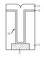
도 1a 및 도 1b는 종래 기술에 따른 CVD 텅스텐 공정을 이용한 메탈콘택 제조 방법을 간략히 도시한 도면이다.1A and 1B schematically illustrate a method for manufacturing a metal contact using a CVD tungsten process according to the prior art.
도 1a에 도시된 바와 같이, 하부 금속배선(11) 상부에 금속간절연막(IMD, 12)을 형성한 후, 금속간절연막(12)을 식각하여 하부 금속배선(11)의 일부를 노출시키는 콘택홀(13)을 형성한다.As shown in FIG. 1A, after forming the intermetal insulation layer (IMD) 12 on the
다음으로, 콘택홀(13)을 포함한 전면에 확산방지막(14)을 증착한 후, 확산방지막(14) 상에 콘택홀(13)을 채울때까지 CVD 텅스텐 공정을 통해 텅스텐막(15)을 증착한다. 이때, 확산방지막(14)으로는 화학기상증착법(CVD)을 이용하여 증착한 티타늄막과 티타늄나이트라이드막의 적층구조(TiN/Ti)를 이용하고, 텅스텐막(15)의 화학기상증착시 소스가스로는 육불화텅스텐(WF6) 가스를 이용한다.Next, after the
도 1b에 도시된 바와 같이, 층간절연막(12)의 표면이 드러날때까지 화학적기 계적연마 또는 에치백하여 콘택홀(13) 내에만 확산방지막(14)과 텅스텐막(15a)을 잔류시킨다. 이때, 잔류하는 텅스텐막(15a)을 '텅스텐플러그(15a)'라 한다. 여기서, 텅스텐플러그(15a)는 하부 금속배선(11)과 상부금속배선을 연결시키는 메탈콘택 역할을 한다.As shown in FIG. 1B, chemical mechanical polishing or etch back is performed until the surface of the
다음으로, 텅스텐플러그(15a) 상에 접착막으로서 티타늄나이트라이드막(16)을 증착하고, 티타늄나이트라이드막(16) 상에 텅스텐막(17)을 증착한다. 그리고, 텅스텐막(17)과 티타늄나이트라이드막(16)을 패터닝하여 상부 금속배선을 형성한다.Next, a
상술한 종래기술에서 확산방지막으로 TiN을 이용하고 있으며, 이 TiN의 웨팅층(wetting layer)으로서 Ti를 사용하고 있다.In the above-mentioned prior art, TiN is used as the diffusion barrier, and Ti is used as the wetting layer of TiN.
소자의 집적도가 증가함에 따라 콘택홀의 종횡비가 급속히 증가하면서 콘택저항을 낮추기 위하여 TiN/Ti 구조의 확산방지막에 대해 많은 변화를 필요로 하고 있는 실정이다. 예를 들어, 100nm 이하의 메모리 소자의 경우, 콘택저항을 낮추기 위하여 Ti를 증착하지 않고 곧바로 얇은 TiN을 화학기상증착법에 의해 증착하는 방법이 제안되었다.As the integration ratio of the device increases, the aspect ratio of the contact hole rapidly increases, and many changes are required for the diffusion barrier of the TiN / Ti structure in order to lower the contact resistance. For example, in the case of a memory device of 100 nm or less, in order to lower contact resistance, a method of depositing thin TiN immediately by chemical vapor deposition has been proposed without depositing Ti.
그러나, 이와 같이 TiN만을 증착하는 경우 하부층인 금속간절연막과 접착력이 나빠지고, TiN이 섬(Island) 형태로 성장(growth)을 하기 때문에 섬이 성장하여 연속된 박막을 형성하기 위해서는 일정 두께 이상으로 TiN을 증착해야만 하는 단점이 있다. 더욱이, TiN의 두께가 두꺼울수록 비저항이 높아지기 때문에 콘택저항의 증가는 피할 수 없다. 즉, 화학기상증착법(CVD)에 의해 증착된 TiN은 주 매립금속 인 텅스텐막보다 비저항이 높은 물질이므로 콘택 저항의 증가를 초래하고, TiN의 확산방지능력을 유지하기 위해 두께를 두껍게 하면 콘택홀 내벽에 비저항이 높은 물질이 두껍게 증착되기 때문에 콘택저항은 더욱 증가한다.However, in the case of depositing only TiN as described above, since the adhesion between the interlayer insulating film, which is a lower layer, and the TiN is grown in the form of islands, the islands grow to form a continuous thin film. There is a drawback to having to deposit TiN. In addition, since the resistivity increases as the thickness of TiN increases, an increase in contact resistance cannot be avoided. That is, TiN deposited by chemical vapor deposition (CVD) has a higher resistivity than the tungsten film, which is the main buried metal, resulting in an increase in contact resistance. The contact resistance is further increased because a high resistivity material is deposited thickly.
위와 같은 콘택저항 증가는 콘택홀의 종횡비가 증가할수록 더욱더 증가하는 문제가 있다.The increase in contact resistance as described above has a problem that increases as the aspect ratio of the contact hole increases.
따라서, 확산방지막의 확산방지 능력이 저하되지 않으면서 가능한 한 얇게 증착할 필요가 있으며, 또한, 하부층과의 접착력(Adhesion) 향상도 반드시 필요한 요건이 되고 있다.Therefore, it is necessary to deposit as thin as possible without deteriorating the diffusion preventing ability of the diffusion barrier film, and furthermore, the improvement of adhesion with the underlying layer is also a necessary requirement.
본 발명은 상기한 종래기술의 문제점을 해결하기 위해 제안된 것으로, 하부층과의 접착력이 우수하면서 확산방지능력을 확보할 수 있는 얇은 두께로 형성할 수 있는 확산방지막을 구비한 반도체소자의 제조 방법을 제공하는데 그 목적이 있다.
The present invention has been proposed to solve the above-mentioned problems of the prior art, and has a method of manufacturing a semiconductor device having a diffusion barrier layer which can be formed in a thin thickness that can secure the diffusion prevention ability while excellent adhesion to the lower layer. The purpose is to provide.
상기 목적을 달성하기 위한 본 발명의 반도체소자의 제조 방법은 금속배선을 덮는 절연막을 형성하는 단계, 상기 절연막을 식각하여 상기 금속배선의 표면 일부를 노출시키는 홀을 형성하는 단계, 상기 홀을 포함한 상기 절연막 표면에 디보란을 이용하여 보론이 흡착된 소우킹층을 형성하는 단계, 상기 소우킹층 상에 확산방지막을 형성하는 단계, 및 상기 확산방지막 상에 상기 홀을 채울때까지 금속막을 매립하는 단계를 포함하는 것을 특징으로 하고, 상기 소우킹층은 디보란 또는 실란을 이용하여 형성하는 것을 특징으로 한다.A method of manufacturing a semiconductor device of the present invention for achieving the above object comprises the steps of forming an insulating film covering the metal wiring, etching the insulating film to form a hole for exposing a portion of the surface of the metal wiring, the including the hole Forming a soaking layer on which the boron is adsorbed using diborane on the surface of the insulating film, forming a diffusion barrier layer on the soaking layer, and embedding a metal layer until the hole is filled on the diffusion barrier layer. The soaking layer is formed using diborane or silane.
또한, 본 발명의 반도체소자의 제조 방법은 실리콘이 함유된 반도체층을 덮는 절연막을 형성하는 단계, 상기 절연막을 식각하여 상기 반도체층의 표면 일부를 노출시키는 홀을 형성하는 단계, 상기 노출된 반도체층 표면에 실리사이드를 형성하는 단계, 상기 실리사이드를 포함한 전면에 디보란을 이용하여 보론이 흡착된 소우킹층을 형성하는 단계, 상기 소우킹층 상에 확산방지막을 형성하는 단계, 및 상기 확산방지막 상에 상기 홀을 채울때까지 금속막을 매립하는 단계를 포함하는 것을 특징으로 한다.In addition, the method of manufacturing a semiconductor device of the present invention comprises the steps of forming an insulating film covering the semiconductor layer containing silicon, etching the insulating film to form a hole for exposing a portion of the surface of the semiconductor layer, the exposed semiconductor layer Forming silicide on the surface, forming a soaking layer on which boron is adsorbed using diborane on the entire surface including the silicide, forming a diffusion barrier on the soaking layer, and forming the hole on the diffusion barrier It is characterized in that it comprises a step of embedding a metal film until filling.
이하, 본 발명이 속하는 기술분야에서 통상의 지식을 가진 자가 본 발명의 기술적 사상을 용이하게 실시할 수 있을 정도로 상세히 설명하기 위하여, 본 발명의 가장 바람직한 실시예를 첨부 도면을 참조하여 설명하기로 한다.Hereinafter, the most preferred embodiments of the present invention will be described in detail with reference to the accompanying drawings so that those skilled in the art may easily implement the technical idea of the present invention. .
후술하는 본 발명의 실시예는 보론을 이용한 소우킹(Soaking) 기술을 도입하여 하부층과의 접착력이 우수하면서 확산방지능력을 확보할 수 있는 얇은 두께로 형성할 수 있는 TiN 확산방지막의 제조 방법을 제안한다.An embodiment of the present invention to be described later proposes a method of manufacturing a TiN diffusion barrier that can be formed in a thin thickness to ensure the diffusion prevention ability while excellent adhesion to the lower layer by introducing a soaking (Soaking) technology using boron. do.
도 2a 내지 도 2d는 본 발명의 실시예에 따른 TiN 확산방지막의 제조 방법을 도시한 공정 단면도이다.2A to 2D are cross-sectional views illustrating a method of manufacturing a TiN diffusion barrier according to an embodiment of the present invention.
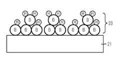
도 2a에 도시된 바와 같이, TiCl4와 NH3 분자의 반응에 의한 TiN의 CVD 공정 에서, 반응이 일어나기 위해 100℃∼800℃ 범위의 온도로 가열된 기판(21)에 먼저 소우킹(Soaking) 물질로서 디보란(B2H6, Diborane)(22)을 도입한다. 이때, 챔버의 압력은 0.1mtorr∼100torr를 유지한다.As shown in FIG. 2A, in the CVD process of TiN by the reaction of TiCl4 and NH3 molecules, first soaking on the
도 2b에 도시된 바와 같이, 디보란(22)을 챔버 내부에 도입하면, 기판(21) 표면에 수 층의 보론층(23)이 형성된다. 여기서, 소우킹은 접착력 증대를 위한 것으로, 확산방지막을 증착하기 전에 표면을 전처리해주어 레이어-바이-레이어(layer-by-layer) 형태로 확산방지막이 성장하도록 도와준다. 이처럼 표면 전처리를 한 층을 소우킹 층이라고 한다.As shown in FIG. 2B, when the
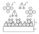
상기한 것처럼 소우킹층인 보론층(23)을 형성한 후에, 도 2c에 도시된 바와 같이, 기판(21) 상부에 TiCl4(24)와 NH3(25)가 포함된 기체를 도입한다.After forming the
다음으로, 도 2d에 도시된 바와 같이, TiCl4(24)와 NH3(25)가 포함된 기체를 챔버 내부에 도입하면, 표면에 흡착된 보론층(23)과 TiCl4와의 빠른 반응특성 때문에 기판(21)의 모든 표면에서 균일하게 빠른 속도로 TiN 핵이 생성되어, 1∼10nm의 얇지만 연속된 TiN 박막(26)이 성장된다. 이때, Cl과 H의 반응부산물들(27)은 휘발된다.Next, as shown in Figure 2d, when the gas containing TiCl4 (24) and NH3 (25) is introduced into the chamber, due to the fast reaction characteristics of the
도 2a 내지 도 2d에 따르면, 균일하게 TiN 핵이 생성되고 보론의 웨팅(wetting) 특성에 의해 TiN 박막(26)의 하부층에 대한 접착력도 크게 향상된다.According to FIGS. 2A to 2D, TiN nuclei are uniformly generated and adhesion to the lower layer of the TiN
위에서는 디보란을 이용하여 소우킹층을 형성하였으나, 실란(SiH4)을 소우킹 물질로 이용할 수 있고, 소우킹층을 플라즈마분위기하에서 전처리하여 형성할 수도 있다. 플라즈마분위기하에서 전처리는 0℃∼800℃ 기판위에서 RF 또는 DC 전원을 이용하여 소우킹 물질이 포함된 반응기내에 직접 플라즈마를 형성하여 전처리하거나, 아르곤 등 불활성기체의 리모트플라즈마(Remote plasma)를 이용하여 소우킹 물질을 활성화하고, 활성화된 소우킹물질에 의해 기판 표면을 전처리할 수 있다.Although a soaking layer is formed using diborane, the silane (SiH4 ) may be used as a soaking material, and the soaking layer may be formed by pretreatment under a plasma atmosphere. In the plasma atmosphere, pretreatment is performed by directly forming plasma in a reactor containing soaking material using RF or DC power on a substrate at 0 ° C to 800 ° C, or by using a remote plasma of an inert gas such as argon. The king material may be activated and the substrate surface may be pretreated by the activated soaking material.
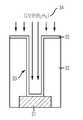
도 3a 내지 도 3d는 도2의 확산방지막 형성 공정을 금속배선 위에 형성되는 콘택 제조 방법에 적용한 경우를 도시한 공정 단면도이다.3A to 3D are cross-sectional views illustrating a case where the diffusion barrier film forming process of FIG. 2 is applied to a contact manufacturing method formed on a metal wiring.
도 3a에 도시된 바와 같이, 하부 금속배선(31) 상부에 층간절연막 또는 금속간절연막(32)을 형성한 후, 금속간절연막(32)을 식각하여 하부 금속배선(31)의 일부를 노출시키는 콘택홀(33)을 형성한다. 하부 금속배선(31)은 W, Al, Cu, Ti, TiN, TaN, Ta, WN이 적용가능하고, 상부 금속배선으로는 텅스텐막외에도 Al, Cu가 적용 가능하다.As shown in FIG. 3A, after forming the interlayer insulating film or the intermetallic insulating
도 3b에 도시된 바와 같이, 400℃∼700℃ 범위의 온도를 유지하는 TiN CVD 증착챔버 내에 소우킹 물질로서 디보란(B2H6, 34)을 도입하면, 콘택홀(33)을 포함한 전면에 디보란의 흡착층(35)이 형성된다. 여기서, 흡착층(35)은 디보란 중의 보론이 흡착된 것으로, 서브 모노레이어부터 수 모노레이어로 성장한다.As shown in FIG. 3B, when diborane (B2 H6 , 34) is introduced as a soaking material into the TiN CVD deposition chamber maintaining a temperature in the range of 400 ° C. to 700 ° C., the front surface including the
도 3c에 도시된 바와 같이, 흡착층(35)을 형성한 후에, 챔버에 TiCl4와 NH3가 포함된 기체(36)를 도입하면 흡착층(35)과 TiCl4와의 빠른 반응특성 때문에 모든 표면에서 균일하게 빠른 속도로 TiN 핵이 생성되어 1∼10nm의 얇지만 연속된 TiN 박막(37)이 성장된다. 이때, Cl과 H의 반응부산물들은 휘발된다.As shown in FIG. 3C, after the formation of the
도 3d에 도시된 바와 같이, TiN 박막(37)을 증착한 후, TiN 박막(37) 상에 콘택홀(33)을 채울때까지 CVD 텅스텐 공정을 통해 텅스텐막(38)을 증착한다. 이때,텅스텐막(38)의 화학기상증착시 소스가스로는 육불화텅스텐(WF6) 가스를 이용한다.As shown in FIG. 3D, after depositing the TiN
상기한 실시예에서, 소우킹 물질을 도입하는 공정은 TiN CVD 챔버와 별개의 챔버에서 진행할 수도 있으나, CVD 챔버와 동일한 챔버에서 인시튜로 진행하면공정 쓰루풋 향상과 비용절감을 구현할 수 있다.In the above embodiment, the process of introducing the soaking material may be performed in a chamber separate from the TiN CVD chamber, but proceeding in situ in the same chamber as the CVD chamber may realize process throughput and cost reduction.
상술한 실시예는 하부 금속배선(31) 위에 콘택이 형성되는 경우 확산방지막인 TiN 박막(37)을 형성한 경우이며, TiN 박막(37)은 얇고 균일하며 흡착층(35) 위에 형성되므로 접착력이 우수하다.In the above-described embodiment, when the contact is formed on the
도 4a 내지 도 4e는 도 2의 확산방지막 공정을 실리콘 위에 형성되는 콘택 제조 방법에 적용한 제1예를 도시한 공정 단면도이다.4A to 4E are cross-sectional views illustrating a first example in which the diffusion barrier film process of FIG. 2 is applied to a contact manufacturing method formed on silicon.
도 4a에 도시된 바와 같이, 실리콘이 함유된 반도체층(41) 상부에 층간절연막(42)을 형성한 후, 층간절연막(42)을 식각하여 반도체층(41)의 일부를 노출시키는 콘택홀(43)을 형성한다.As shown in FIG. 4A, after forming the
도 4b에 도시된 바와 같이, TiCl4와 수소(H2)를 포함하는 CVD Ti 공정을 진행한다.As shown in FIG. 4B, a CVD Ti process including TiCl4 and hydrogen (H2 ) is performed.
위와 같은 CVD Ti 공정을 통해 티타늄막(Ti, 44)을 증착하는데, 티타늄막(44)은 콘택홀(43) 아래의 반도체층(41) 표면, 콘택홀(43)의 내벽 그리고, 층간절연막(42) 표면에 증착된다.The titanium film Ti is deposited through the CVD Ti process as described above. The
한편, 티타늄막(44) 증착시 실리콘이 함유된 반도체층(41)과 티타늄막(44)이 반응하여 콘택홀 아래의 반도체층(41) 상에는 티타늄실리사이드(TiSi2, 45)이 형성된다.Meanwhile, when the
위와 같이, CVD Ti 공정과 동시에 티타늄실리사이드(45)가 형성되는 원리는 CVD Ti 공정이 고온에서 이루어지기 때문에 별도의 열처리없이 티타늄실리사이드를 티타늄막 증착과 동시에 형성할 수 있는 것이다.As described above, the principle that the
도 4c에 도시된 바와 같이, 티타늄막(44)이 증착된 기판을 400℃∼700℃ 범위의 온도를 유지하는 TiN CVD 증착챔버로 이동한 후, 챔버내에 소우킹 물질로서 디보란(B2H6, 46)을 도입하면, 티타늄막(44) 표면에 디보란의 흡착층(47)이 형성된다. 여기서, 흡착층(47)은 디보란 중의 보론이 흡착된 것으로, 서브 모노레이어부터 수 모노레이어로 성장한다.As shown in FIG. 4C, the substrate on which the
도 4d에 도시된 바와 같이, 흡착층(47)을 형성한 후에, 챔버에 TiCl4와 NH3가 포함된 기체(48)를 도입하면 흡착층(47)과 TiCl4와의 빠른 반응특성 때문에 모든 표면에서 균일하게 빠른 속도로 TiN 핵이 생성되어 1∼10nm의 얇지만 연속된 TiN 박막(49)이 성장된다. 이때, Cl과 H의 반응부산물들은 휘발된다.As shown in FIG. 4D, after the
후속 공정으로, 도 4e에 도시된 바와 같이, TiN 박막(49) 상에 콘택홀(43)을 채울때까지 CVD 텅스텐 공정을 통해 텅스텐막(50)을 증착한다. 이때, 텅스텐막의 화학기상증착시 소스가스로는 육불화텅스텐(WF6) 가스를 이용한다.In a subsequent process, as shown in FIG. 4E, the
상술한 도 4a 내지 도 4e는 실리콘이 함유된 반도체층(41) 위에 콘택이 형성되는 경우 콘택저항 감소를 위해 콘택 부위에 티타늄실리사이드(45)를 형성한 후 확산방지막인 TiN 박막(49)을 형성한 경우이며, TiCl4와 NH3를 이용한 TiN 박막(49) 증착시 티타늄실리사이드(45)에 파손을 초래할 수 있는 TiCl4에 포함된 클로린(Cl)의 어택을 억제할 수 있는 장점이 있다. 이와 같은 어택을 억제하는 것은 흡착층(47)이 막아주기 때문이다.4A to 4E, when the contact is formed on the silicon-containing
상기한 실리사이드로는 티타늄실리사이드외에 탄탈륨실리사이드(TaSi), 텅스텐실리사이드(WSi), 코발트실리사이드(CoSi), 니켈실리사이드(NiSi)가 적용 가능하고, 이로써 티타늄막외에 탄탈륨(Ta), 텅스텐(W), 코발트(Co), 니켈(Ni)이 적용 가능하다.As the silicide, tantalum silicide (TaSi), tungsten silicide (WSi), cobalt silicide (CoSi), nickel silicide (NiSi) in addition to titanium silicide may be applied, and thus tantalum (Ta), tungsten (W), Cobalt (Co) and nickel (Ni) are applicable.
도 5a 내지 도 5e는 도 2의 확산방지막 공정을 실리콘 위에 형성되는 콘택 제조 방법에 적용한 제2예를 도시한 공정 단면도이다.5A through 5E are cross-sectional views illustrating a second example in which the diffusion barrier film process of FIG. 2 is applied to a contact manufacturing method formed on silicon.
도 5a에 도시된 바와 같이, 실리콘이 함유된 반도체층(51) 상부에 층간절연막(52)을 형성한 후, 층간절연막(52)을 식각하여 반도체층(51)의 일부를 노출시키는 콘택홀(53)을 형성한다.As shown in FIG. 5A, after forming the
도 5b에 도시된 바와 같이, 살리사이드 공정(Salicide process)을 진행하여 콘택홀(53) 아래에 노출된 반도체층(51) 표면에 직접 티타늄실리사이드(54)를 형성한다.As shown in FIG. 5B, a salicide process is performed to form
여기서, 살리사이드 공정은 물리기상증착법(PVD)을 이용한 Ti 공정을 통해 티타늄막(Ti)을 증착한 후, 일정 열처리를 실시하여 실리콘이 함유된 반도체층(51)과 티타늄막의 반응을 유도하여 콘택홀(53) 아래의 반도체층(51) 상에 티타늄실리사이드(TiSi2, 54)를 형성한다. 다음으로, 미반응 티타늄막을 제거해준다.Here, in the salicide process, a titanium film (Ti) is deposited through a Ti process using physical vapor deposition (PVD), and then a predetermined heat treatment is performed to induce a reaction between the
도 5c에 도시된 바와 같이, 티타늄실리사이드(54)가 형성된 기판을 400℃∼700℃ 범위의 온도를 유지하는 TiN CVD 증착챔버로 이동한 후, 챔버내에 소우킹 물질로서 디보란(B2H6, 55)을 도입하면, 티타늄실리사이드(54)를 포함한 층간절연막(52) 표면에 디보란의 흡착층(56)이 형성된다. 여기서, 흡착층(56)은 디보란 중의 보론이 흡착된 것으로, 서브 모노레이어부터 수 모노레이어로 성장한다.As shown in FIG. 5C, the substrate on which the
도 5d에 도시된 바와 같이, 흡착층(56)을 형성한 후에, 챔버에 TiCl4와 NH3가 포함된 기체(57)를 도입하면 흡착층(56)과 TiCl4와의 빠른 반응특성 때문에 모든 표면에서 균일하게 빠른 속도로 TiN 핵이 생성되어 1∼10nm의 얇지만 연속된 TiN 박막(58)이 성장된다. 이때, Cl과 H의 반응부산물들은 휘발된다.As shown in FIG. 5D, after the
도 5e에 도시된 바와 같이, TiN 박막(58)을 증착한 후, TiN 박막(58) 상에 콘택홀(53)을 채울때까지 CVD 텅스텐 공정을 통해 텅스텐막(59)을 증착한다. 이때,텅스텐막(59)의 화학기상증착시 소스가스로는 육불화텅스텐(WF6) 가스를 이용한다.As shown in FIG. 5E, after depositing the TiN
상술한 제3실시예는 실리콘이 함유된 반도체층(51) 위에 콘택이 형성되는 경우 콘택저항 감소를 위해 콘택 부위에 티타늄실리사이드(54)를 형성한 후 확산방지 막인 TiN 박막(58)을 형성한 경우이며, TiCl4와 NH3를 이용한 TiN 박막(58) 증착시 티타늄실리사이드(54)에 파손을 초래할 수 있는 TiCl4에 포함된 클로린(Cl)의 어택을 억제할 수 있는 장점이 있다. 이와 같은 어택을 억제하는 것은 흡착층(56)이 막아주기 때문이다.In the third embodiment described above, when a contact is formed on a
상기한 실리사이드로는 티타늄실리사이드외에 탄탈륨실리사이드(TaSi), 텅스텐실리사이드(WSi), 코발트실리사이드(CoSi), 니켈실리사이드(NiSi)가 적용 가능하다.In addition to titanium silicide, tantalum silicide (TaSi), tungsten silicide (WSi), cobalt silicide (CoSi), and nickel silicide (NiSi) may be used as the silicide.
본 발명의 기술 사상은 상기 바람직한 실시예에 따라 구체적으로 기술되었으나, 상기한 실시예는 그 설명을 위한 것이며 그 제한을 위한 것이 아님을 주의하여야 한다. 또한, 본 발명의 기술 분야의 통상의 전문가라면 본 발명의 기술 사상의 범위 내에서 다양한 실시예가 가능함을 이해할 수 있을 것이다.Although the technical idea of the present invention has been described in detail according to the above preferred embodiment, it should be noted that the above-described embodiment is for the purpose of description and not of limitation. In addition, those skilled in the art will understand that various embodiments are possible within the scope of the technical idea of the present invention.
예컨대, 반도체소자 제조 공정중 확산방지막으로 사용하는 TaN, WN, TiW, 비정질 메탈(Amorphous metal)도 소우킹 기술을 도입하여 하부층과의 접착력이 우수하면서 확산방지능력을 확보할 수 있는 얇은 두께로 균일하게 형성할 수 있다.For example, TaN, WN, TiW, and Amorphous metal, which are used as diffusion barriers in the manufacturing process of semiconductor devices, are also adopted with soaking technology to provide excellent adhesion to the underlying layer and uniform thickness with a thin thickness to ensure diffusion prevention capability. Can be formed.
상술한 본 발명은 종횡비가 큰 고집적 반도체 메모리 소자의 메탈콘택저항을 감소시킬 수 있으며, CVD 텅스텐의 확산방지막으로 사용하는 TiCl4 기저의 CVD TiN 박막의 하부층과의 접착력을 향상시킬 수 있는 효과가 있다.The present invention described above can reduce the metal contact resistance of a high density semiconductor memory device having a high aspect ratio, and can improve the adhesion to the lower layer of the CVD TiN thin film based on TiCl4 used as a diffusion barrier of CVD tungsten. .
또한, TiN 박막의 치밀도가 좋기 때문에 확산방지막으로서의 특성이 개선되며, 소우킹 물질의 흡착층이 있는 상태에서 확산방지막이 CVD 공정을 통해 형성되기 때문에 CVD의 전구체에서 발생할 수 있는 오염원(할로겐원소)으로부터 하부층이 보호받을 수 있는 효과가 있다.In addition, since the TiN thin film has a high density, the characteristics of the diffusion barrier are improved, and since the diffusion barrier is formed through the CVD process in the presence of an adsorption layer of soaking material, a source of contamination (halogen element) that may occur in the precursor of CVD There is an effect that the lower layer can be protected from.
Claims (15)
Translated fromKoreanPriority Applications (4)
| Application Number | Priority Date | Filing Date | Title |
|---|---|---|---|
| KR1020040031921AKR100578221B1 (en) | 2004-05-06 | 2004-05-06 | Method for manufacturing semiconductor device having diffusion barrier |
| TW093137700ATWI270151B (en) | 2004-05-06 | 2004-12-07 | Method for fabricating semiconductor device having diffusion barrier layer |
| US11/020,750US20050250321A1 (en) | 2004-05-06 | 2004-12-21 | Method for fabricating semiconductor device having diffusion barrier layer |
| CNA2004101041698ACN1694238A (en) | 2004-05-06 | 2004-12-30 | Method for fabricating semiconductor device having diffusion barrier layer |
Applications Claiming Priority (1)
| Application Number | Priority Date | Filing Date | Title |
|---|---|---|---|
| KR1020040031921AKR100578221B1 (en) | 2004-05-06 | 2004-05-06 | Method for manufacturing semiconductor device having diffusion barrier |
Publications (2)
| Publication Number | Publication Date |
|---|---|
| KR20050106863A KR20050106863A (en) | 2005-11-11 |
| KR100578221B1true KR100578221B1 (en) | 2006-05-12 |
Family
ID=35239974
Family Applications (1)
| Application Number | Title | Priority Date | Filing Date |
|---|---|---|---|
| KR1020040031921AExpired - Fee RelatedKR100578221B1 (en) | 2004-05-06 | 2004-05-06 | Method for manufacturing semiconductor device having diffusion barrier |
Country Status (4)
| Country | Link |
|---|---|
| US (1) | US20050250321A1 (en) |
| KR (1) | KR100578221B1 (en) |
| CN (1) | CN1694238A (en) |
| TW (1) | TWI270151B (en) |
Families Citing this family (8)
| Publication number | Priority date | Publication date | Assignee | Title |
|---|---|---|---|---|
| JP4523535B2 (en)* | 2005-08-30 | 2010-08-11 | 富士通株式会社 | Manufacturing method of semiconductor device |
| JP5171192B2 (en)* | 2007-09-28 | 2013-03-27 | 東京エレクトロン株式会社 | Metal film formation method |
| KR101406276B1 (en)* | 2007-11-29 | 2014-06-27 | 삼성전자주식회사 | METAL WIRING OF SEMICONDUCTOR DEVICE |
| US20170309490A1 (en)* | 2014-09-24 | 2017-10-26 | Hitachi Kokusai Electric Inc. | Method of manufacturing semiconductor device |
| JP6937604B2 (en)* | 2017-04-26 | 2021-09-22 | 東京エレクトロン株式会社 | How to form a tungsten film |
| US10535527B2 (en)* | 2017-07-13 | 2020-01-14 | Applied Materials, Inc. | Methods for depositing semiconductor films |
| JP2021136273A (en)* | 2020-02-25 | 2021-09-13 | キオクシア株式会社 | Semiconductor device and manufacturing method for the same |
| CN114242688B (en)* | 2020-09-09 | 2025-03-25 | 中芯国际集成电路制造(上海)有限公司 | Semiconductor device and method for forming the same |
Family Cites Families (18)
| Publication number | Priority date | Publication date | Assignee | Title |
|---|---|---|---|---|
| KR100349999B1 (en)* | 1990-04-24 | 2002-12-11 | 세이코 엡슨 가부시키가이샤 | Semiconductor device with ferroelectric and manufacturing method |
| JP3129232B2 (en)* | 1997-05-08 | 2001-01-29 | 日本電気株式会社 | Method for manufacturing semiconductor device |
| US5821168A (en)* | 1997-07-16 | 1998-10-13 | Motorola, Inc. | Process for forming a semiconductor device |
| US6284316B1 (en)* | 1998-02-25 | 2001-09-04 | Micron Technology, Inc. | Chemical vapor deposition of titanium |
| US6653222B2 (en)* | 1999-08-03 | 2003-11-25 | International Business Machines Corporation | Plasma enhanced liner |
| US6482733B2 (en)* | 2000-05-15 | 2002-11-19 | Asm Microchemistry Oy | Protective layers prior to alternating layer deposition |
| US6620723B1 (en)* | 2000-06-27 | 2003-09-16 | Applied Materials, Inc. | Formation of boride barrier layers using chemisorption techniques |
| US6936538B2 (en)* | 2001-07-16 | 2005-08-30 | Applied Materials, Inc. | Method and apparatus for depositing tungsten after surface treatment to improve film characteristics |
| KR100343653B1 (en)* | 2000-09-22 | 2002-07-11 | 윤종용 | Semiconductor device with metal silicide layer and method of manufacturing the same |
| US6455428B1 (en)* | 2000-10-26 | 2002-09-24 | Vanguard International Semiconductor Corporation | Method of forming a metal silicide layer |
| US6284653B1 (en)* | 2000-10-30 | 2001-09-04 | Vanguard International Semiconductor Corp. | Method of selectively forming a barrier layer from a directionally deposited metal layer |
| US7005372B2 (en)* | 2003-01-21 | 2006-02-28 | Novellus Systems, Inc. | Deposition of tungsten nitride |
| TW589684B (en)* | 2001-10-10 | 2004-06-01 | Applied Materials Inc | Method for depositing refractory metal layers employing sequential deposition techniques |
| US6911391B2 (en)* | 2002-01-26 | 2005-06-28 | Applied Materials, Inc. | Integration of titanium and titanium nitride layers |
| US6939538B2 (en)* | 2002-04-11 | 2005-09-06 | Biomedical Research Models, Inc. | Extended release analgesic for pain control |
| US6974768B1 (en)* | 2003-01-15 | 2005-12-13 | Novellus Systems, Inc. | Methods of providing an adhesion layer for adhesion of barrier and/or seed layers to dielectric films |
| US7211508B2 (en)* | 2003-06-18 | 2007-05-01 | Applied Materials, Inc. | Atomic layer deposition of tantalum based barrier materials |
| US6841466B1 (en)* | 2003-09-26 | 2005-01-11 | Taiwan Semiconductor Manufacturing Company | Method of selectively making copper using plating technology |
- 2004
- 2004-05-06KRKR1020040031921Apatent/KR100578221B1/ennot_activeExpired - Fee Related
- 2004-12-07TWTW093137700Apatent/TWI270151B/ennot_activeIP Right Cessation
- 2004-12-21USUS11/020,750patent/US20050250321A1/ennot_activeAbandoned
- 2004-12-30CNCNA2004101041698Apatent/CN1694238A/enactivePending
Also Published As
| Publication number | Publication date |
|---|---|
| KR20050106863A (en) | 2005-11-11 |
| TWI270151B (en) | 2007-01-01 |
| TW200537628A (en) | 2005-11-16 |
| US20050250321A1 (en) | 2005-11-10 |
| CN1694238A (en) | 2005-11-09 |
Similar Documents
| Publication | Publication Date | Title |
|---|---|---|
| EP0869544B1 (en) | Method for depositing a diffusion barrier | |
| KR100599434B1 (en) | Metal wiring formation method of semiconductor device | |
| US7504333B2 (en) | Method of forming bit line of semiconductor device | |
| KR101615292B1 (en) | Method for forming a film stack on a substrate | |
| KR100455382B1 (en) | Method for forming metal interconnections of semiconductor device having dual damascene structure | |
| TWI694501B (en) | Dielectric/metal barrier integration to prevent copper diffusion | |
| US8946074B2 (en) | Method of making interconnect structure | |
| KR100407684B1 (en) | Method of manufacturing a semiconductor device | |
| KR20020072875A (en) | Method for forming metal wiring layer | |
| KR100578221B1 (en) | Method for manufacturing semiconductor device having diffusion barrier | |
| KR20050011479A (en) | Method for Forming Tungsten Contact Plug of Semiconductor Device | |
| JP4804725B2 (en) | Method for forming conductive structure of semiconductor device | |
| US6245674B1 (en) | Method of forming a metal silicide comprising contact over a substrate | |
| JP2004179605A (en) | Aluminum metal wiring forming method | |
| JP2002057125A (en) | Method of forming metal wiring | |
| US8159069B2 (en) | Metal line of semiconductor device without production of high resistance compound due to metal diffusion and method for forming the same | |
| KR100727437B1 (en) | Metal wiring formation method | |
| JP2004363402A (en) | Method for manufacturing semiconductor device | |
| KR100743632B1 (en) | Manufacturing method of semiconductor device | |
| KR20020056293A (en) | Method for forming metal line in semiconductor device | |
| KR100780627B1 (en) | Semiconductor device having carbonized barrier layer and manufacturing method thereof | |
| KR100606246B1 (en) | Formation method of high purity CO thin film having excellent applicability and low specific resistance and contact plug formation method of semiconductor device using the same | |
| KR100571387B1 (en) | Copper wiring manufacturing method of semiconductor device | |
| KR101096444B1 (en) | Metal wiring formation method of semiconductor device | |
| JPH053171A (en) | Forming method of tungsten plug |
Legal Events
| Date | Code | Title | Description |
|---|---|---|---|
| A201 | Request for examination | ||
| PA0109 | Patent application | St.27 status event code:A-0-1-A10-A12-nap-PA0109 | |
| PA0201 | Request for examination | St.27 status event code:A-1-2-D10-D11-exm-PA0201 | |
| D13-X000 | Search requested | St.27 status event code:A-1-2-D10-D13-srh-X000 | |
| D14-X000 | Search report completed | St.27 status event code:A-1-2-D10-D14-srh-X000 | |
| E902 | Notification of reason for refusal | ||
| PE0902 | Notice of grounds for rejection | St.27 status event code:A-1-2-D10-D21-exm-PE0902 | |
| PG1501 | Laying open of application | St.27 status event code:A-1-1-Q10-Q12-nap-PG1501 | |
| E13-X000 | Pre-grant limitation requested | St.27 status event code:A-2-3-E10-E13-lim-X000 | |
| P11-X000 | Amendment of application requested | St.27 status event code:A-2-2-P10-P11-nap-X000 | |
| P13-X000 | Application amended | St.27 status event code:A-2-2-P10-P13-nap-X000 | |
| E701 | Decision to grant or registration of patent right | ||
| PE0701 | Decision of registration | St.27 status event code:A-1-2-D10-D22-exm-PE0701 | |
| GRNT | Written decision to grant | ||
| PR0701 | Registration of establishment | St.27 status event code:A-2-4-F10-F11-exm-PR0701 | |
| PR1002 | Payment of registration fee | St.27 status event code:A-2-2-U10-U11-oth-PR1002 Fee payment year number:1 | |
| PG1601 | Publication of registration | St.27 status event code:A-4-4-Q10-Q13-nap-PG1601 | |
| LAPS | Lapse due to unpaid annual fee | ||
| PC1903 | Unpaid annual fee | St.27 status event code:A-4-4-U10-U13-oth-PC1903 Not in force date:20090503 Payment event data comment text:Termination Category : DEFAULT_OF_REGISTRATION_FEE | |
| PC1903 | Unpaid annual fee | St.27 status event code:N-4-6-H10-H13-oth-PC1903 Ip right cessation event data comment text:Termination Category : DEFAULT_OF_REGISTRATION_FEE Not in force date:20090503 | |
| PN2301 | Change of applicant | St.27 status event code:A-5-5-R10-R13-asn-PN2301 St.27 status event code:A-5-5-R10-R11-asn-PN2301 | |
| PN2301 | Change of applicant | St.27 status event code:A-5-5-R10-R13-asn-PN2301 St.27 status event code:A-5-5-R10-R11-asn-PN2301 | |
| PN2301 | Change of applicant | St.27 status event code:A-5-5-R10-R13-asn-PN2301 St.27 status event code:A-5-5-R10-R11-asn-PN2301 |