KR100577410B1 - X-ray image sensing device and its manufacturing method - Google Patents
X-ray image sensing device and its manufacturing methodDownload PDFInfo
- Publication number
- KR100577410B1 KR100577410B1KR1019990053712AKR19990053712AKR100577410B1KR 100577410 B1KR100577410 B1KR 100577410B1KR 1019990053712 AKR1019990053712 AKR 1019990053712AKR 19990053712 AKR19990053712 AKR 19990053712AKR 100577410 B1KR100577410 B1KR 100577410B1
- Authority
- KR
- South Korea
- Prior art keywords
- electrode
- source
- forming
- contact
- substrate
- Prior art date
- Legal status (The legal status is an assumption and is not a legal conclusion. Google has not performed a legal analysis and makes no representation as to the accuracy of the status listed.)
- Expired - Lifetime
Links
Images


Classifications
- H—ELECTRICITY
- H10—SEMICONDUCTOR DEVICES; ELECTRIC SOLID-STATE DEVICES NOT OTHERWISE PROVIDED FOR
- H10D—INORGANIC ELECTRIC SEMICONDUCTOR DEVICES
- H10D30/00—Field-effect transistors [FET]
- H10D30/60—Insulated-gate field-effect transistors [IGFET]
- H10D30/67—Thin-film transistors [TFT]
- H—ELECTRICITY
- H10—SEMICONDUCTOR DEVICES; ELECTRIC SOLID-STATE DEVICES NOT OTHERWISE PROVIDED FOR
- H10F—INORGANIC SEMICONDUCTOR DEVICES SENSITIVE TO INFRARED RADIATION, LIGHT, ELECTROMAGNETIC RADIATION OF SHORTER WAVELENGTH OR CORPUSCULAR RADIATION
- H10F39/00—Integrated devices, or assemblies of multiple devices, comprising at least one element covered by group H10F30/00, e.g. radiation detectors comprising photodiode arrays
- H10F39/80—Constructional details of image sensors
- H10F39/803—Pixels having integrated switching, control, storage or amplification elements
- H—ELECTRICITY
- H10—SEMICONDUCTOR DEVICES; ELECTRIC SOLID-STATE DEVICES NOT OTHERWISE PROVIDED FOR
- H10F—INORGANIC SEMICONDUCTOR DEVICES SENSITIVE TO INFRARED RADIATION, LIGHT, ELECTROMAGNETIC RADIATION OF SHORTER WAVELENGTH OR CORPUSCULAR RADIATION
- H10F39/00—Integrated devices, or assemblies of multiple devices, comprising at least one element covered by group H10F30/00, e.g. radiation detectors comprising photodiode arrays
- H10F39/011—Manufacture or treatment of image sensors covered by group H10F39/12
- H10F39/016—Manufacture or treatment of image sensors covered by group H10F39/12 of thin-film-based image sensors
- H—ELECTRICITY
- H10—SEMICONDUCTOR DEVICES; ELECTRIC SOLID-STATE DEVICES NOT OTHERWISE PROVIDED FOR
- H10F—INORGANIC SEMICONDUCTOR DEVICES SENSITIVE TO INFRARED RADIATION, LIGHT, ELECTROMAGNETIC RADIATION OF SHORTER WAVELENGTH OR CORPUSCULAR RADIATION
- H10F39/00—Integrated devices, or assemblies of multiple devices, comprising at least one element covered by group H10F30/00, e.g. radiation detectors comprising photodiode arrays
- H10F39/011—Manufacture or treatment of image sensors covered by group H10F39/12
- H10F39/018—Manufacture or treatment of image sensors covered by group H10F39/12 of hybrid image sensors
- H—ELECTRICITY
- H10—SEMICONDUCTOR DEVICES; ELECTRIC SOLID-STATE DEVICES NOT OTHERWISE PROVIDED FOR
- H10F—INORGANIC SEMICONDUCTOR DEVICES SENSITIVE TO INFRARED RADIATION, LIGHT, ELECTROMAGNETIC RADIATION OF SHORTER WAVELENGTH OR CORPUSCULAR RADIATION
- H10F39/00—Integrated devices, or assemblies of multiple devices, comprising at least one element covered by group H10F30/00, e.g. radiation detectors comprising photodiode arrays
- H10F39/10—Integrated devices
- H10F39/12—Image sensors
- H10F39/191—Photoconductor image sensors
- H10F39/195—X-ray, gamma-ray or corpuscular radiation imagers
Landscapes
- Solid State Image Pick-Up Elements (AREA)
Abstract
Translated fromKoreanDescription
Translated fromKorean도 1은 엑스레이 영상 감지소자의 동작을 나타내는 단면도.1 is a cross-sectional view showing the operation of the X-ray image sensing device.
도 2는 종래 엑스레이 영상 감지소자의 한 화소부분에 해당하는 단면을 나타내는 단면도.2 is a cross-sectional view showing a cross section corresponding to one pixel portion of a conventional X-ray image sensing device.
도 3a 내지 도 3f는 도 2의 절단선 Ⅲ-Ⅲ 방향으로 자른 단면의 제작 공정을 도시한 공정도.3A to 3F are process diagrams illustrating a fabrication process of a cross section taken along the cutting line III-III of FIG. 2.
도 4는 도 3f의 S 부분을 확대한 단면도.4 is an enlarged cross-sectional view of part S of FIG. 3F;
도 5a 내지 도 5e는 본 발명에 따른 엑스레이 영상 감지소자의 제작 공정을 도시한 공정도.5a to 5e is a process chart showing a manufacturing process of the x-ray image sensing device according to the present invention.
〈도면의 주요부분에 대한 부호의 설명〉<Explanation of symbols for main parts of drawing>
1 : 기판 (Glass) 200 : 게이트 전극 1: Glass 200: Gate Electrode
202 : 게이트 절연막 204 : 비정질 실리콘202: gate insulating film 204: amorphous silicon
206 : 불순물 비정질 실리콘 208 : 반도체층206: impurity amorphous silicon 208: semiconductor layer
210 : 드레인 전극 212 : 소스 전극210: drain electrode 212: source electrode
214 : 접지배선 216 : 보호막214: grounding wiring 216: protective film
224 : 전하인출전극 222 : 스토리지 전극224: charge extraction electrode 222: storage electrode
230 : 화소전극 226 : 유전체230: pixel electrode 226: dielectric
T : 박막 트랜지스터 Cst : 스토리지 캐패시터 T: Thin Film Transistor Cst: Storage Capacitor
본 발명은 TFT 어레이 공정을 이용한 엑스레이 영상 감지소자 및 그 제조방법에 관한 것이다.The present invention relates to an X-ray image sensing device using a TFT array process and a method of manufacturing the same.
현재 의학용으로 널리 사용되고 있는 진단용 엑스레이(X-ray) 검사방법은 엑스레이 감지 필름을 사용하여 촬영하고, 그 결과를 알기 위해서는 소정의 필름 인화시간을 거쳐야 했다.Diagnostic X-ray (X-ray) test method, which is widely used for medical purposes today, is photographed using an X-ray detection film, and a predetermined film print time has to be passed in order to know the result.
그러나, 근래에 들어서 반도체 기술의 발전에 힘입어 박막 트랜지스터(Thin Film Transistor)를 이용한 디지털 엑스레이 디텍터(Digital X-ray detector ; 이하 엑스레이 영상감지소자라 칭한다)가 연구/개발되었다. 상기 엑스레이 영상감지소자는 박막 트랜지스터를 스위칭 소자로 사용하여, 엑스레이의 촬영 즉시 실시간으로 결과를 진단할 수 있는 장점이 있다.However, in recent years, with the development of semiconductor technology, digital X-ray detectors (hereinafter referred to as X-ray image sensing devices) using thin film transistors have been researched and developed. The X-ray image sensing device has a merit of diagnosing a result in real time immediately after imaging of the X-ray using a thin film transistor as a switching device.
이하, 엑스레이 영상감지소자의 구성과 그 동작을 살펴보면 다음과 같다.Hereinafter, the configuration and operation of the X-ray image sensing device will be described.
도 1은 엑스레이 영상감지소자(100)의 구성 및 작용을 설명하는 개략도로서, 하부에 기판(1)이 형성되어 있고, 박막 트랜지스터(3), 스토리지 캐패시터(10), 화소 전극(12), 광도전막(2), 보호막(20), 전극(24), 고압 직류전원(26) 등으로 구성된다.1 is a schematic diagram illustrating the configuration and operation of the X-ray
상기 광도전막(2)은 입사되는 전기파나 자기파등 외부의 신호강도에 비례하여 내부적으로 전기적인 신호 즉, 전자 및 정공쌍(6)을 형성한다. 상기 광도전막(2)은 외부의 신호, 특히 엑스레이를 전기적인 신호로 변환하는 변환기의 역할을 한다. 엑스레이 광에 의해 형성된 전자-정공쌍(6)은 광도전막(2) 상부에 위치하는 도전전극(24)에 고압 직류전원(26)에서 인가된 전압(Ev)에 의해 광도전막(2) 하부에 위치하는 화소전극(12)에 전하의 형태로 모여지고, 외부에서 접지된 공통전극과 함께 형성된 스토리지 캐패시터(10)에 저장된다. 이 때, 상기 스토리지 캐패시터(10)에 저장된 전하는 외부에서 제어하는 상기 박막 트랜지스터(3)에 의해 외부의 영상 처리소자로 보내지고 엑스레이 영상을 만들어 낸다.The
그런데, 엑스레이 영상 감지소자에서 약한 엑스레이 광이라도 이를 탐지하여 전하로 변환시키기 위해서는 광도전막(2) 내에서 전하를 트랩 하는 트랩 상태밀도 수를 줄이고, 도전전극(24)과 화소 전극(12) 사이에 수직으로 큰 전압(10V/μm 이상)을 인가하여 수직방향이외의 전압에 의해 흐르는 전류를 줄여야 한다.However, in order to detect even the weak X-ray light and convert it into a charge in the X-ray image sensing device, the number of trap state densities trapping the charge in the
엑스레이 광에 의해 생성된 광도전막(2) 내의 전하들이 화소 전극뿐만 아니라 박막 트랜지스터(3)의 채널부분을 보호하는 보호막 상부에도 트랩되어 모인다. 이렇게 트랩되어 모여진 전하는 박막 트랜지스터(3) 상부의 채널영역에 전하를 유 도하여 박막 트랜지스터(3)가 오프 상태일 때도 큰 누설전류를 발생시켜 박막 트랜지스터(3)가 스위칭 동작을 할 수 없게 한다.Charges in the
또한, 스토리지 캐패시터(10)에 저장된 전기적인 신호가 오프 상태에서의 큰 누설전류 때문에 외부로 흐르게 되어, 얻고자 하는 영상을 제대로 표현하지 못하는 현상이 생길 수 있다.In addition, the electrical signal stored in the
도 2는 종래의 엑스레이 영상 감지소자(100)의 한 화소부를 나타낸 평면도로서, 게이트 배선(50)이 행 방향으로 배열되어 있고, 드레인 배선(52)이 열 방향으로 배열되어 있다. 또, 게이트 배선(50)과 드레인 배선(52)이 직교하는 부분에 스위칭 소자로써 박막 트랜지스터(3)가 형성되고, 일 방향으로 인접한 인접화소와 공통적으로 접지 되어 있는 공통전극으로 접지배선(42)이 배열되어 있다.2 is a plan view showing one pixel portion of a conventional X-ray
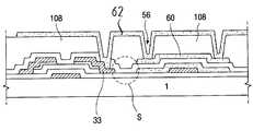
그리고, 전하 저장수단으로서 스토리지 캐패시터(S)를 구성하게끔 제 1 투명전극(58)과 제 2 투명전극(60)이 형성되어 있고, 유전물질로 실리콘 질화막(미도시)이 상기 제 1 및 제 2 투명전극 사이에 삽입 형성되어 있다.The first
또한, 화소 전극으로 제 3 투명전극(62)이 상기 박막 트랜지스터(3) 상부까지 연장되어 형성되며, 도시하지는 않았지만 광도전막에서 발생한 정공(hole)이 스토리지 캐패시터(S)내에 축적될 수 있도록 상기 제 2 투명전극(60)과 전기적으로 연결되고, 상기 스토리지 캐패시터(S) 내에 저장된 정공이 상기 박막 트랜지스터(3)를 통해 들어오는 전자(electron)와 결합할 수 있도록 소스 콘택홀(54)을 통해 소스전극(33)과 전기적으로 연결되어 있다.In addition, a third
상술한 엑스레이 영상감지소자의 기능을 요약하면 다음과 같다.The function of the above-described X-ray image sensing device is summarized as follows.
광도전막(미도시)으로 부터 생성된 정공은 한 화소로서 역할을 하는 제 3 투명전극(62)으로 모이고, 상기 제 3 투명전극(62)과 전기적으로 연결되고 스토리지 캐패시터(S)의 일 전극으로서 동작하는 제 2 투명전극(60)을 통해 상기 스토리지 캐패시터(S)에 저장된다. 상기 스토리지 캐패시터(S)에 저장된 정공은 박막 트랜지스터(3)의 동작에 의해 소스 전극(33)과 연결된 제 3 투명전극(62)을 통해 드레인 전극(32)으로 이동하고, 외부의 회로(미도시)에서 영상으로 표현한다.Holes generated from the photoconductive film (not shown) are collected into a third
상기 제 1, 2, 3 투명전극은 각각 스토리지 제 1 , 2 전극 및 화소 전극으로서의 역할을 한다.The first, second, and third transparent electrodes serve as storage first, second electrodes, and pixel electrodes, respectively.
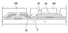
도 3a ∼도 3f에 도시된 바와 같이, 엑스레이 영상 감지소자의 제작공정을 도 2의 절단선 Ⅲ-Ⅲ으로 자른 단면에 따라 설명한다.As shown in FIGS. 3A to 3F, the manufacturing process of the X-ray image sensing device will be described according to the section taken along the cutting line III-III of FIG. 2.
먼저, 도 3a를 참조하여 설명하면, 기판(1) 상에 알루미늄 또는 알루미늄 합금과 같은 금속을 증착하여 수직단면이 테이퍼 형상을 가지도록 게이트 전극(31)을 형성한다.First, referring to FIG. 3A, a metal such as aluminum or an aluminum alloy is deposited on the
기판(1)으로는 절연물질의 고융점을 가지는 고가의 석영판과 저온 공정에서 주로 사용되는 유리기판이 쓰이는데, 본 실시예는 절연물질의 기판으로 유리기판을 사용한다. 그리고, 상기 게이트 전극(31)은 몰리브덴(Mo), 탄탈(Ta), 텅스텐(W), 니노븀(Nb) 또는 안티몬(Sb)등과 같은 고융점을 가지는 금속을 사용할 수 있다.As the
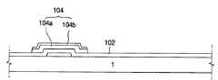
도 3b는 제 1 절연막 및 반도체층을 증착하는 단계로, 4000Å 두께의 실리콘 질화막(SiNx) 또는 실리콘 산화막(SiOx)과 같은 무기 절연막을 증착하거나, 경우에 따라서는 BCB(Benzocyclobutene) 또는 아크릴(Acryl)계 수지와 같은 유기 절연물질 을 도포하여 게이트 절연막(102)을 형성한다. 본 발명의 바람직한 실시예에서는 실리콘 질화막을 증착하여 사용한다.FIG. 3B is a step of depositing a first insulating film and a semiconductor layer, and depositing an inorganic insulating film such as a silicon nitride film (SiNx) or a silicon oxide film (SiOx) having a thickness of 4000 Å, or in some cases, benzocyclobutene (BCB) or acrylic (Acryl) The
이후, 반도체층(104)을 형성하는 단계로, 순수 비정질 실리콘과 같은 반도체막(104a)과 불순물이 첨가된 비정질 실리콘막(104b)을 연속으로 증착한다. 불순물이 첨가된 비정질 실리콘막(104b)의 형성은 기상 증착법과 이온 주입법이 있으나 본 실시예는 기상 증착법을 따른다.Thereafter, in the step of forming the
도 3c는 제 2 금속층으로 소스 및 드레인 전극(33, 32)과, 접지배선(42)을 형성하는 단계로, 크롬(Cr) 또는 크롬합금(Cr alloy)과 같은 금속을 증착하고, 패터닝하여 소스전극(33), 드레인 전극(32), 접지배선(42) 등을 형성한다.3C is a step of forming source and
또한, 소스 및 드레인 전극(33, 32)을 마스크로 하여 박막 트랜지스터의 채널이 될 부분 즉, 소스전극(33) 및 드레인 전극(32) 사이에 불순물이 첨가된 비정질 실리콘막(104b)만을 제거한다. 이렇게 해서 스위칭 소자로 쓰이는 박막 트랜지스터(C)가 만들어진다.In addition, only the
이후, 상기 접지배선(42)과 접촉하게끔, ITO와 같은 투명전극을 사용하여 제 1 스토리지 전극(58)을 상기 접지배선(42) 상에 형성한다.Thereafter, the
도 3d는 상기 박막 트랜지스터(C)와 제 1 스토리지 전극(58) 및 기판 전면에 걸쳐 제 2 절연막으로 3000Å 두께의 실리콘 질화막을 증착하여 스토리지 캐패시터의 유전체와 박막 트랜지스터(C)의 보호막으로 사용되는 절연막(106)을 형성하는 단계를 도시한 도면이다.FIG. 3D is an insulating film used as a protective film for the dielectric of the storage capacitor and the thin film transistor C by depositing a 3000 Å thick silicon nitride film with the second insulating film over the thin film transistor C, the
이후, 상기 제 1 스토리지 전극(58) 상부 상기 절연막(106) 상에 투명전극을 사용하여 제 2 스토리지 전극(60)을 형성하며, 상기 제 2 스토리지 전극(60)은 상기 제 1 스토리지 전극(58) 상부에 상기 제 1 스토리지 전극(58)과 크거나 같은 크기로 형성한다.Thereafter, a
도 3e는 제 3 절연막의 보호막(108)을 형성하는 단계로 유기질의 BCB(benzocyclobutene)를 사용하였다. 상기 BCB는 유전율이 기존의 실리콘 질화막이나, 실리콘 산화막 또는 아크릴과 비교해서 매우 낮은 물질이다.3E uses organic BCB (benzocyclobutene) as a step of forming the
상기 보호막(108) 증착 후에 스토리지 콘택홀(56)을 형성하는데, 상기 소스전극(33) 및 상기 제 2 스토리지 전극(60)의 일부가 드러나도록 형성한다.A
도 3f는 투명전극을 사용하여 화소전극(62)을 형성하는 단계로, 도 3e공정에서 형성된 스토리지 콘택홀(56)을 충진 시키면서 증착한다. 즉, 상기 화소전극(62)은 상기 소스전극(33)과 제 2 스토리지 전극(60)과 전기적으로 접촉된다. 3F is a step of forming a
또한, 상기 화소전극(62)은 종래의 머쉬룸 구조를 사용하기 위해 상기 박막 트랜지스터(C)의 상부까지 연장하여 형성한다.In addition, the
다음 공정은 도시하지 않았지만, 감광성 물질을 도포 하는 단계로, 감광성 물질은 외부의 신호를 받아서 전기적인 신호로 변환하는 변환기로 쓰이는데, 비정질 셀레니움(selenium)의 화합물을 진공증착기(evaporator)를 이용하여 100-500㎛ 두께로 증착한다. 또한, HgI2, PbO, CdTe, CdSe, 탈륨브로마이드, 카드뮴설파이드 등과 같은 종류의 암전도도가 작고 외부신호에 민감한, 특히 엑스레이 광전도도가 큰 엑스레이 감광성물질을 사용할 수 있다. 엑스레이 광이 감광물질에 노출되면 노출 광의 세기에 따라 감광물질 내에 전자 및 정공쌍이 발생한다.Although the following process is not shown, the photosensitive material is applied to the photosensitive material. The photosensitive material is used as a transducer for receiving an external signal and converting the signal into an electrical signal. The compound of amorphous selenium is converted into a vacuum using an evaporator. Deposit at -500 μm thickness. In addition, an X-ray photosensitive material having a low dark conductivity and sensitive to an external signal, particularly X-ray photoconductivity, may be used, such as HgI2 , PbO, CdTe, CdSe, thallium bromide, cadmium sulfide, and the like. When the X-ray light is exposed to the photosensitive material, electrons and hole pairs are generated in the photosensitive material according to the intensity of the exposed light.
엑스레이 감광물질 도포 후에 엑스레이 광이 투과될 수 있도록 투명한 도전 전극을 형성한다. 도전전극에 전압을 인가하면서 엑스레이 광을 받아들이면 감광물질 내에 형성된 전자 및 정공쌍은 서로 분리되고, 화소 전극(62)에는 상기 도전전극에 의해 분리된 정공이 모여 스토리지 캐패시터(S)에 저장된다.After applying the X-ray photosensitive material, a transparent conductive electrode may be formed to transmit X-ray light. When the X-ray light is applied while applying a voltage to the conductive electrode, electrons and hole pairs formed in the photosensitive material are separated from each other, and holes separated by the conductive electrode are collected in the
상술한 바와 같은 종래의 엑스레이 영상 감지소자에서는 스토리지 캐패시터(S)를 형성하기 위해 투명전극인 ITO의 증착과 패터닝 공정이 3회나 실시되므로 작업공정 수가 많고 복잡할 뿐아니라, ITO 식각용액에 의한 게이트 배선/전극과 소스 및 드레인 전극이 침식되는 문제가 있다.In the conventional X-ray image sensing device as described above, since the deposition and patterning process of the transparent electrode ITO is performed three times to form the storage capacitor S, the number of work processes is large and complicated, and the gate wiring by the ITO etching solution is performed. There is a problem that the electrodes and the source and drain electrodes are eroded.
또한, 도 4에 도시된 도면에서와 같이 제 1 스토리지 전극(58)과 소스 전극(33)의 간격(△L)이 좁기 때문에 단락(short)의 발생시 상기 제 1 스토리지 전극(58)과 전기적으로 접촉하는 접지배선과의 단락으로 이어져 선결함(line defect)이 발생할 수 있는 단점이 있다.In addition, as shown in FIG. 4, since the gap ΔL between the
또한, 드래인 배선(52)과 제 1 투명전극(58) 간의 기생용량에 의한 신호지영 등의 노이즈가 발생하는 문제가 있다.In addition, there is a problem that noise such as signal reception due to parasitic capacitance between the
본 발명은 상기의 문제점을 해결하기 위해 안출된 것으로, 엑스레이 영상 감지소자를 제조하는데 있어서, 그 공정수를 저감하는데 그 목적이 있다.SUMMARY OF THE INVENTION The present invention has been made to solve the above problems, and an object thereof is to reduce the number of steps in manufacturing an X-ray image sensing device.
또한, 소스 및 드레인 전극과 스토리지 전극간의 단락을 줄여 수율을 향상하는데 그 목적이 있다.
In addition, the purpose is to improve the yield by reducing the short circuit between the source and drain electrodes and the storage electrode.
상기와 같은 목적을 달성하기 위해 본 발명에서는 기판; 기판 상에 형성된 게이트 전극; 상기 게이트 전극과 기판을 덮는 게이트 절연막; 상기 게이트 절연막 상의 소정 위치에 형성된 접지배선; 상기 게이트 전극 상부 상기 게이트 절연막 상에 형성된 액티브층; 상기 액티브층 상에 형성된 소스 및 드레인 전극; 상기 소스 및 드레인 전극과 상기 접지배선이 형성된 기판의 전면을 덮고, 상기 접지배선과 상기 소스 전극의 일부가 각각 노출되게 제 1 및 제 2 콘택홀을 갖는 보호막; 상기 보호막 상에 형성되고, 상기 제 1 콘택홀을 통해 상기 접지배선과 접촉하는 스토리지 전극; 상기 보호막의 상기 제 2 콘택홀을 통해 상기 소스 전극과 접촉하는 전하인출전극; 상기 스토리지 전극과 상기 전하인출전극의 전면을 덮고, 상기 전하인출전극의 일부가 노출되도록 제 3 콘택홀을 갖는 유전층; 상기 유전층 상에 형성되고, 상기 제 3 콘택홀을 통해 상기 전하인출전극과 접촉하는 화소전극을 포함하는 엑스레이 영상 감지소자을 제공한다.In the present invention to achieve the above object; A gate electrode formed on the substrate; A gate insulating layer covering the gate electrode and the substrate; A ground wiring formed at a predetermined position on the gate insulating film; An active layer formed on the gate insulating layer on the gate electrode; Source and drain electrodes formed on the active layer; A passivation layer covering an entire surface of the substrate on which the source and drain electrodes and the ground wiring are formed, and having first and second contact holes to expose the ground wiring and a portion of the source electrode, respectively; A storage electrode formed on the passivation layer and contacting the ground line through the first contact hole; A charge extraction electrode in contact with the source electrode through the second contact hole of the passivation layer; A dielectric layer covering an entire surface of the storage electrode and the charge extraction electrode and having a third contact hole to expose a portion of the charge extraction electrode; An X-ray image sensing device is formed on the dielectric layer and includes a pixel electrode contacting the charge extracting electrode through the third contact hole.
그리고, 본 발명에서는 기판을 구비하는 단계와; 상기 기판 상에 게이트 전극을 형성하는 단계와; 상기 게이트 전극이 형성된 기판 상의 전면에 걸쳐 게이트 절연막, 비정질 실리콘, 불순물 비정질 실리콘을 순차적으로 증착하고 패터닝하여 액티브층을 형성하는 단계와; 상기 액티브층 상에 소스 및 드레인 전극을 형성하 고, 상기 소스 및 드레인 전극과 동일 물질로 게이트 절연막 상에 접지배선을 형성하는 단계와; 상기 소스 및 드레인 전극과 접지배선이 형성된 기판의 전면에 걸쳐 유기절연막을 증착하고, 상기 접지배선과 상기 소스 전극의 일부분이 각각 노출되도록 제 1 및 제 2 콘택홀을 형성하는 단계와; 상기 제 1 및 제 2 콘택홀이 형성된 유기절연막 상에 상기 제 1 콘택홀을 통해 상기 접지배선과 접촉하는 스토리지 전극과, 상기 제 2 콘택홀을 통해 상기 소스 전극과 접촉하는 전하인출전극을 형성하는 단계와; 상기 스토리지 전극과 전하인출전극이 형성된 기판의 전면에 걸쳐 유전층을 증착하고, 상기 전하인출전극의 일부가 노출된 제 3 콘택홀을 형성하는 단계와; 상기 유전층 상에 상기 전하인출전극과 접촉하는 화소전극을 형성하는 단계와; 상기 화소 전극 상에 광도전막을 형성하는 단계와; 상기 광도전막 상에 도전 전극을 형성하는 단계를 포함하는 엑스레이 영상 감지소자 제조방법을 제공한다.In addition, the present invention comprises the steps of providing a substrate; Forming a gate electrode on the substrate; Sequentially depositing and patterning a gate insulating film, amorphous silicon, and impurity amorphous silicon over the entire surface of the substrate on which the gate electrode is formed to form an active layer; Forming a source and a drain electrode on the active layer, and forming a ground wiring on the gate insulating layer using the same material as the source and drain electrodes; Depositing an organic insulating film over the entire surface of the substrate on which the source and drain electrodes and the ground wiring are formed, and forming first and second contact holes to expose the ground wiring and a portion of the source electrode, respectively; Forming a storage electrode in contact with the ground line through the first contact hole and a charge extraction electrode in contact with the source electrode through the second contact hole on the organic insulating layer on which the first and second contact holes are formed; Steps; Depositing a dielectric layer over the entire surface of the substrate on which the storage electrode and the charge extraction electrode are formed, and forming a third contact hole through which a portion of the charge extraction electrode is exposed; Forming a pixel electrode on the dielectric layer in contact with the charge extracting electrode; Forming a photoconductive film on the pixel electrode; It provides an X-ray image sensing device manufacturing method comprising the step of forming a conductive electrode on the photoconductive film.
이하, 본 발명의 실시예에 따른 구성과 작용을 첨부된 도면을 참조하여 설명한다.Hereinafter, the configuration and operation according to the embodiment of the present invention will be described with reference to the accompanying drawings.
도 5a 내지 도 5e는 본 발명의 실시예에 따른 엑스레이 영상 감지소자의 제작공정을 도시한 공정도로써, 본 발명에 따른 엑스레이 영상 감지소자에서는 스토리지 캐패시터를 형성할 때, 두 개의 전극만을 사용하는 것을 특징으로 한다. 5A to 5E are process charts illustrating a manufacturing process of an X-ray image sensing device according to an exemplary embodiment of the present invention. In the X-ray image sensing device according to the present invention, only two electrodes are used to form a storage capacitor. It is done.
도 5a는 기판(1) 상에 제 1 금속을 증착하고, 패터닝하여 게이트 전극(200)을 형성하는 단계를 도시한 도면이다. 상기 게이트 전극(200)은 실질적으로 불투명한 금속을 사용한다.FIG. 5A illustrates a step of depositing and patterning a first metal on the
도 5b는 반도체층(208)을 형성하는 단계를 도시한 도면이다.5B illustrates a step of forming the
먼저, 상기 게이트 전극(200)이 형성된 기판(1) 상에 게이트 절연막(202)과 비정질 실리콘(204)과, 불순물이 함유된 비정질 실리콘(206)을 연속으로 증착한후, 상기 게이트 절연막(202)의 상부까지 식각하여 반도체층(208)을 형성한다.First, the
상기 반도체층(208)은 다결정 실리콘을 사용하여 형성할 수 있다.The
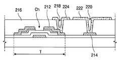
도 5c는 소스 및 드레인 전극(212, 210)과 공통전극으로 접지배선(214)을 형성하는 단계를 도시한 도면이다.5C is a diagram illustrating a step of forming a
상기 소스 및 드레인 전극(212, 210)과 접지배선(214)을 형성하기 위해 먼저, 상기 반도체층(208)과 상기 반도체층(208)에 의해 노출된 게이트 절연막(202) 상에 제 2 금속을 증착하고, 상기 반도체층(208) 상에 상기 게이트 전극(200)과 각각 소정의 길이로 오버랩되게 패터닝하여 소스 및 드레인 전극(212, 210)을 형성하고, 상기 게이트 절연막(202) 상에 형성된 제 2 금속층을 패터닝하여 접지배선(214)을 형성한다.In order to form the source and drain
이후, 상기 소스 및 드레인 전극(212, 210)을 마스크로하여 상기 소스 및 드레인 전극(212, 210) 사이에 존재하는 불순물이 함유된 비정질 실리콘(206)을 식각하여 채널(Ch)을 형성한다. 상기 채널(Ch)이 형성되면 스위칭 소자로써의 기능을 할 수 있게 된다. 즉, 박막 트랜지스터(T)가 완성되는 것이다.Subsequently, the channel Ch is formed by etching the
상기 접지배선(214)은 추후에 동작 설명에서 상술되겠지만 스토리지 캐패시터내에 잔류하는 잔류전하를 제거하는 기능(reset)을 하게 된다.The
도 5d는 스토리지 전극(222)을 형성하는 단계를 도시한 도면이다.5D is a diagram illustrating the formation of the
상기 스토리지 전극(222) 형성전에 먼저, 상기 박막 트랜지스터(T)와 접지배선(214) 상에 보호막(216)을 증착하고 패터닝하여, 상기 소스전극(212)과 접지배선(214)의 일부가 노출되도록 소스 콘택홀(218)과 접지배선 콘택홀(220)을 각각 형성한다.Before forming the
이후, 제 1 투명전극을 증착하고 패터닝하여, 상기 소스 콘택홀(218)을 통해 상기 소스 전극(212)과 접촉하는 소스 인출전극(224)과 상기 접지배선 콘택홀(220)을 통해 상기 접지배선(214)과 접촉하는 스토리지 전극(222)을 형성한다.Thereafter, a first transparent electrode is deposited and patterned, and the source lead-out
상기 보호막(216)은 실질적으로 빛에 투명한 재질을 사용하며, 유기 절연막인 벤조사이클로뷰틴(benzocyclobutene ; BCB)을 사용하며, 상기 BCB는 평탄화율이우수하고, 유전율이 약 3 이하로 작기 때문에 보호막으로 사용하기에는 좋은 재질이다.The
또한, 상기 보호막(216)은 아크릴, 폴리이미드 등이 사용될 수 있다.In addition, the
도 5e는 상기 소스 인출전극(224)과 스토리지 전극(222)이 형성된 기판(1) 상에 유전체(226)와 화소전극(230)을 형성하는 단계를 도시한 도면이다.5E illustrates a step of forming a dielectric 226 and a
상기 유전체(226)에는 상기 소스 인출전극(224)의 일부가 노출된 접속홀(228)이 형성되며, 상기 접속홀(228)을 통해 상기 소스 인출전극(224)과 접촉하는 화소전극(230)이 형성된다.In the dielectric 226, a
상기 화소전극(230)이 형성됨으로써, 스토리지 캐패시터(Cst)는 형성된다. 즉, 상기 스토리지 전극(222)을 일 전극으로 하고, 상기 화소전극(230)을 타전극으로 하며, 상기 스토리지 전극(222)과 상기 화소전극(230)의 사이에 존재하는 유전 체(226)로써 상기 스토리지 캐패시터(Cst)는 형성된다.By forming the
다음 공정은 도시하지 않았지만, 감광성 물질을 도포 하는 단계로, 감광성 물질은 외부의 신호를 받아서 전기적인 신호로 변환하는 변환기로 쓰이는데, 비정질 셀레니움(selenium)의 화합물을 진공증착기(evaporator)를 이용하여 100-500㎛ 두께로 증착한다. 또한, HgI2, PbO, CdTe, CdSe, 탈륨브로마이드, 카드뮴설파이드 등과 같은 종류의 암전도도가 작고 외부신호에 민감한, 특히 엑스레이 광전도도가 큰 엑스레이 감광성물질을 사용할 수 있다. 엑스레이 광이 감광물질에 조사되면 조사 광의 세기에 따라 감광물질 내에 전자 및 정공쌍이 발생한다.Although the following process is not shown, the photosensitive material is applied to the photosensitive material. The photosensitive material is used as a transducer for receiving an external signal and converting the signal into an electrical signal. The compound of amorphous selenium is converted into a vacuum using an evaporator. Deposit at -500 μm thickness. In addition, an X-ray photosensitive material having a low dark conductivity and sensitive to an external signal, particularly X-ray photoconductivity, may be used, such as HgI2 , PbO, CdTe, CdSe, thallium bromide, cadmium sulfide, and the like. When X-ray light is irradiated to the photosensitive material, electrons and hole pairs are generated in the photosensitive material according to the intensity of the irradiated light.
엑스레이 감광물질 도포 후에 엑스레이 광이 투과될 수 있도록 투명한 도전 전극을 형성한다.After applying the X-ray photosensitive material, a transparent conductive electrode may be formed to transmit X-ray light.
상술한 본 발명에 따른 엑스레이 영상 감지소자의 동작을 설명하면 다음과 같다.The operation of the X-ray image sensing device according to the present invention described above is as follows.
상기 감광성 물질이 엑스레이 광에 노출되면 내부적으로는 전자/정공쌍이 형성되고, 이 때, 상기 도전전극에 강한 직류전압을 인가하면, 상기 전자/정공쌍 중 한 성분(전자 또는 정공)이 상기 화소전극(230)에 모이게 된다.When the photosensitive material is exposed to X-ray light, an electron / hole pair is formed internally, and when a strong DC voltage is applied to the conductive electrode, one component (electron or hole) of the electron / hole pair is the pixel electrode. Are gathered at 230.
상기 화소전극(230)에 집전된 전자 또는 정공은 상기 스토리지 캐패시터(Cst)에 전하의 형태로 저장되고, 이 때, 상기 박막 트랜지스터(T)의 게이트 전극(200)에 신호를 인가하면, 상기 스토리지 캐패시터(Cst)에 저장된 전하는 외부의 구동회로(미도시)로 방출되어 이미지로 표현되게 된다.Electrons or holes collected in the
그리고, 스위칭 작용이 끝난 후에도 상기 스토리지 캐패시터(Cst)에 전하가 존재할 경우 상기 스토리지 캐패시터(Cst)와 접촉하는 상기 접지배선(214)을 통해 상기 스토리지 캐패시터(Cst)에 존재하는 잔류전하를 제거한다. 즉, 상기 접지배선(214)은 리셋(reset) 기능을 하게되는 것이다.In addition, when charge is present in the storage capacitor Cst even after the switching operation is completed, residual charge existing in the storage capacitor Cst is removed through the
상술한 엑스레이 영상 감지소자의 각 구성요소의 기능은 다음과 같다.The function of each component of the above-described X-ray image sensing device is as follows.
첫째로는 외부의 엑스레이광을 감지하여 전하를 생성하는 감광성 도전막과 도전전극은 광전변환부로써의 기능을 하게되고, 둘째는 상기 광전변환부에서 생성된 전하를 저장하는 스토리지 캐패시터는 전하저장부로써의 기능을 하게 된다. 그리고, 셋째로는 상기 전하저장부에 저장된 전하를 외부의 구동회로로 전달하는 박막 트랜지스터는 스위칭부로써의 기능을 하게 된다.First, the photosensitive conductive layer and the conductive electrode which generate charge by sensing external X-ray light function as a photoelectric conversion part. Second, the storage capacitor which stores the charge generated in the photoelectric conversion part is a charge storage part. It will function as. Third, the thin film transistor which transfers the charge stored in the charge storage unit to an external driving circuit functions as a switching unit.
상술한 바와 같이, 본 발명의 실시예를 따라 엑스레이 영상 감지소자를 제작할 경우 다음과 같은 효과가 있다.As described above, when manufacturing the X-ray image sensing device according to an embodiment of the present invention has the following effects.
첫째, 종래의 엑스레이 영상 감지소자가 스토리지 캐패시터를 형성하기 위해 세 번의 투명전극의 공정을 거쳤으나, 본 발명에 따른 엑스레이 영상 감지소자의 스토리지 캐패시터는 두 번의 투명전극의 공정 즉, 스토리지 전극과 화소전극으로 형성되어, 제작공정이 간단한 장점이 있다.First, although the conventional X-ray image sensing device has undergone three transparent electrodes to form a storage capacitor, the storage capacitor of the X-ray image sensing device according to the present invention has a process of two transparent electrodes, that is, a storage electrode and a pixel electrode. Is formed, the manufacturing process has a simple advantage.
둘째, 두 번의 투명전극 형성공정으로 스토리지 캐패시터를 형성할 수 있으므로, 제작 수율이 향상되는 장점이 있다.Second, since the storage capacitor can be formed by two transparent electrode forming processes, the manufacturing yield is improved.
셋째, 스토리지 캐패시터를 형성하기 위해 두 번의 투명전극 공정이 사용됨으로, 상기 투명전극의 식각액에 의한 게이트 및 소스/드레인 전극의 침식을 억제할 수 있기 때문에 불량율이 저감되는 장점이 있다.Third, since two transparent electrode processes are used to form a storage capacitor, an erosion rate of the gate and the source / drain electrodes due to the etchant of the transparent electrode can be suppressed, thereby reducing the defective rate.
넷째, 유전율이 낮은 보호막을 먼저 형성한 후, 스토리지 전극을 형성하기 때문에 드레인 배선에 영향을 주는 기생용량을 억제시킴으로서, 노이즈를 줄일 수 있는 장점이 있다.
Fourth, since the protective film having a low dielectric constant is formed first, and then the storage electrode is formed, the parasitic capacitance affecting the drain wiring can be suppressed, thereby reducing noise.
Claims (9)
Translated fromKoreanPriority Applications (3)
| Application Number | Priority Date | Filing Date | Title |
|---|---|---|---|
| KR1019990053712AKR100577410B1 (en) | 1999-11-30 | 1999-11-30 | X-ray image sensing device and its manufacturing method |
| US09/722,654US6399962B1 (en) | 1999-11-30 | 2000-11-28 | X-ray image sensor and method for fabricating the same |
| US10/067,846US6660555B2 (en) | 1999-11-30 | 2002-02-08 | X-ray image sensor and method for fabricating the same |
Applications Claiming Priority (1)
| Application Number | Priority Date | Filing Date | Title |
|---|---|---|---|
| KR1019990053712AKR100577410B1 (en) | 1999-11-30 | 1999-11-30 | X-ray image sensing device and its manufacturing method |
Publications (2)
| Publication Number | Publication Date |
|---|---|
| KR20010048866A KR20010048866A (en) | 2001-06-15 |
| KR100577410B1true KR100577410B1 (en) | 2006-05-08 |
Family
ID=19622601
Family Applications (1)
| Application Number | Title | Priority Date | Filing Date |
|---|---|---|---|
| KR1019990053712AExpired - LifetimeKR100577410B1 (en) | 1999-11-30 | 1999-11-30 | X-ray image sensing device and its manufacturing method |
Country Status (2)
| Country | Link |
|---|---|
| US (2) | US6399962B1 (en) |
| KR (1) | KR100577410B1 (en) |
Families Citing this family (23)
| Publication number | Priority date | Publication date | Assignee | Title |
|---|---|---|---|---|
| JP4103391B2 (en)* | 1999-10-14 | 2008-06-18 | 信越半導体株式会社 | Manufacturing method of SOI wafer and SOI wafer |
| US6825496B2 (en)* | 2001-01-17 | 2004-11-30 | Semiconductor Energy Laboratory Co., Ltd. | Light emitting device |
| JP4037117B2 (en)* | 2001-02-06 | 2008-01-23 | 株式会社日立製作所 | Display device |
| TW458288U (en)* | 2001-03-08 | 2001-10-01 | Liau Guo Fu | X-ray image sensor |
| KR100448448B1 (en)* | 2001-07-12 | 2004-09-13 | 주식회사 디알텍 | Switching element of X-ray panel and the same method |
| KR100852516B1 (en)* | 2001-12-31 | 2008-08-14 | 비오이 하이디스 테크놀로지 주식회사 | Method for manufacturing x-ray detector |
| KR100867473B1 (en)* | 2001-12-31 | 2008-11-06 | 하이디스 테크놀로지 주식회사 | Manufacturing method of X-ray image sensing device |
| AU2003269351A1 (en)* | 2002-10-24 | 2004-05-13 | Koninklijke Philips Electronics N.V. | Method for manufacturing a micro-electromechanical device and micro-electromechanical device obtained therewith |
| WO2006041144A1 (en)* | 2004-10-13 | 2006-04-20 | Semiconductor Energy Laboratory Co., Ltd. | Etching method and manufacturing method of semiconductor device |
| KR101133764B1 (en)* | 2005-03-14 | 2012-04-09 | 삼성전자주식회사 | Thin film transistor, thin film transistor array panel, and manufacturing method thereof |
| US7615731B2 (en)* | 2006-09-14 | 2009-11-10 | Carestream Health, Inc. | High fill-factor sensor with reduced coupling |
| US20080088464A1 (en)* | 2006-09-29 | 2008-04-17 | Gutierrez Francisco M | Power System Architecture for Fluid Flow Measurement Systems |
| KR100889746B1 (en)* | 2007-03-09 | 2009-03-24 | 한국전자통신연구원 | Electronic medical imaging device including chalcogen thin film transistor array |
| TWI337754B (en)* | 2007-04-20 | 2011-02-21 | Au Optronics Corp | Semiconductor structure of display device and method for fabricating the same |
| TWI347680B (en)* | 2007-09-28 | 2011-08-21 | Prime View Int Co Ltd | A photo sensor and a method for manufacturing thereof |
| JP2012027046A (en)* | 2008-11-21 | 2012-02-09 | Sharp Corp | Liquid crystal display device |
| US8215033B2 (en)* | 2009-04-16 | 2012-07-10 | Nike, Inc. | Article of footwear for snowboarding |
| KR101258260B1 (en) | 2010-04-16 | 2013-04-25 | 엘지디스플레이 주식회사 | Organic Light Emitting Display Device |
| US8765514B1 (en)* | 2010-11-12 | 2014-07-01 | L-3 Communications Corp. | Transitioned film growth for conductive semiconductor materials |
| TWI453519B (en)* | 2011-10-03 | 2014-09-21 | Chunghwa Picture Tubes Ltd | Pixel structure of display panel and manufacturing method thereof |
| CN102646676B (en)* | 2011-11-03 | 2015-06-10 | 京东方科技集团股份有限公司 | TFT (thin film transistor) array substrate |
| US9881954B2 (en)* | 2014-06-11 | 2018-01-30 | Semiconductor Energy Laboratory Co., Ltd. | Imaging device |
| US10690787B2 (en)* | 2018-07-16 | 2020-06-23 | Vieworks Co., Ltd. | Radiation imaging system |
Citations (4)
| Publication number | Priority date | Publication date | Assignee | Title |
|---|---|---|---|---|
| JPH0534724A (en)* | 1991-07-31 | 1993-02-12 | Mitsubishi Electric Corp | Ferroelectric liquid crystal cell |
| JPH05100249A (en)* | 1991-10-07 | 1993-04-23 | Fuji Xerox Co Ltd | Active matrix panel and production thereof |
| KR19980077392A (en)* | 1997-04-18 | 1998-11-16 | 김영환 | Thin film transistor liquid crystal display and manufacturing method thereof |
| KR100305275B1 (en)* | 1995-05-07 | 2002-11-04 | 가부시키가이샤 한도오따이 에네루기 켄큐쇼 | Active matrix display device |
Family Cites Families (41)
| Publication number | Priority date | Publication date | Assignee | Title |
|---|---|---|---|---|
| CH456051A (en)* | 1966-06-30 | 1968-05-15 | Contraves Ag | Medical contrast agent injection device |
| US3812843A (en)* | 1973-03-12 | 1974-05-28 | Lear Siegler Inc | Method and apparatus for injecting contrast media into the vascular system |
| US3880138A (en)* | 1973-03-12 | 1975-04-29 | Lear Siegler Inc | Method for injecting contrast media into the vascular system |
| US3888239A (en)* | 1974-06-21 | 1975-06-10 | Morton K Rubinstein | Fluid injection system |
| US4006736A (en)* | 1974-11-27 | 1977-02-08 | Medrad, Inc. | Angiographic injector |
| US4044757A (en)* | 1976-01-14 | 1977-08-30 | The Kendall Company | Cholangiography device and method |
| US4619653A (en)* | 1979-04-27 | 1986-10-28 | The Johns Hopkins University | Apparatus for detecting at least one predetermined condition and providing an informational signal in response thereto in a medication infusion system |
| US4502488A (en)* | 1983-01-13 | 1985-03-05 | Allied Corporation | Injection system |
| US4585009A (en)* | 1983-02-28 | 1986-04-29 | E. R. Squibb & Sons, Inc. | Strontium-rubidium infusion pump with in-line dosimetry |
| US4854324A (en)* | 1984-01-31 | 1989-08-08 | Medrad, Inc. | Processor-controlled angiographic injector device |
| ATE51525T1 (en)* | 1984-06-06 | 1990-04-15 | Medrad Inc | ANGIOGRAPHY INJECTOR AND ANGIOGRAPHY SYRINGE USABLE WITH THEM. |
| US4613328A (en)* | 1984-10-22 | 1986-09-23 | Cecil Boyd | Bio-medical injector apparatus |
| US4695271A (en)* | 1986-02-03 | 1987-09-22 | Liebel-Flarsheim Company | Angiographic injector |
| JPH072182B2 (en)* | 1986-04-07 | 1995-01-18 | テルモ株式会社 | Infusion pump |
| US4737712A (en)* | 1986-12-31 | 1988-04-12 | General Electric Company | Isolated power transfer and patient monitoring system with interference rejection useful with NMR apparatus |
| US5134373A (en)* | 1988-03-31 | 1992-07-28 | Kabushiki Kaisha Toshiba | Magnetic resonance imaging apparatus employing optical viewing screen |
| JPH01277547A (en)* | 1988-04-28 | 1989-11-08 | Hitachi Ltd | MR imaging device with dialogue device |
| US4885538A (en)* | 1988-08-19 | 1989-12-05 | The Regents Of The University Of California | Low data rate low noise serial digital communication link for magnetic resonance imaging systems |
| GB2229497B (en)* | 1989-03-10 | 1992-06-03 | Graseby Medical Ltd | Infusion pump |
| US5030201A (en)* | 1989-11-24 | 1991-07-09 | Aubrey Palestrant | Expandable atherectomy catheter device |
| US5027824A (en)* | 1989-12-01 | 1991-07-02 | Edmond Dougherty | Method and apparatus for detecting, analyzing and recording cardiac rhythm disturbances |
| US5300031A (en)* | 1991-06-07 | 1994-04-05 | Liebel-Flarsheim Company | Apparatus for injecting fluid into animals and disposable front loadable syringe therefor |
| DE4119674A1 (en)* | 1991-06-14 | 1992-12-17 | Spectrospin Ag | ACTUATOR |
| US5464014A (en)* | 1991-10-03 | 1995-11-07 | Sugan Company Limited | Display device for bioelectrical and biophysical phenomena |
| US5269762A (en)* | 1992-04-21 | 1993-12-14 | Sterling Winthrop, Inc. | Portable hand-held power assister device |
| US5342298A (en)* | 1992-07-31 | 1994-08-30 | Advanced Cardiovascular Systems, Inc. | Automated fluid pressure control system |
| US5352979A (en)* | 1992-08-07 | 1994-10-04 | Conturo Thomas E | Magnetic resonance imaging with contrast enhanced phase angle reconstruction |
| FR2695503B1 (en)* | 1992-09-04 | 1994-10-21 | Thomson Csf | Wireless medical data transmission system. |
| US5236417A (en)* | 1992-09-22 | 1993-08-17 | Utah Pioneer Medical, Inc. | Cholangiography catheter apparatus and method |
| US5354273A (en)* | 1992-12-14 | 1994-10-11 | Mallinckrodt Medical, Inc. | Delivery apparatus with pressure controlled delivery |
| US5357959A (en)* | 1993-04-16 | 1994-10-25 | Praxair Technology, Inc. | Altered dipole moment magnetic resonance imaging method |
| US5411485A (en)* | 1993-04-19 | 1995-05-02 | Hyprotek | Catheter access system and method |
| US5472403A (en)* | 1993-05-11 | 1995-12-05 | The Regents Of The University Of California | Device for automatic injection of radionuclide |
| US5417213A (en)* | 1993-06-07 | 1995-05-23 | Prince; Martin R. | Magnetic resonance arteriography with dynamic intravenous contrast agents |
| DE4329898A1 (en)* | 1993-09-04 | 1995-04-06 | Marcus Dr Besson | Wireless medical diagnostic and monitoring device |
| US5494036A (en)* | 1993-11-26 | 1996-02-27 | Medrad, Inc. | Patient infusion system for use with MRI |
| US5693567A (en)* | 1995-06-07 | 1997-12-02 | Xerox Corporation | Separately etching insulating layer for contacts within array and for peripheral pads |
| JP3729953B2 (en)* | 1996-12-02 | 2005-12-21 | コーニンクレッカ フィリップス エレクトロニクス エヌ ヴィ | TFT array substrate and its manufacturing method |
| KR19990003712A (en)* | 1997-06-26 | 1999-01-15 | 김영환 | Ultra high aperture liquid crystal display device and manufacturing method thereof |
| US5994984A (en)* | 1997-11-13 | 1999-11-30 | Carnegie Mellon University | Wireless signal distribution in a building HVAC system |
| US6277679B1 (en)* | 1998-11-25 | 2001-08-21 | Semiconductor Energy Laboratory Co., Ltd. | Method of manufacturing thin film transistor |
- 1999
- 1999-11-30KRKR1019990053712Apatent/KR100577410B1/ennot_activeExpired - Lifetime
- 2000
- 2000-11-28USUS09/722,654patent/US6399962B1/ennot_activeExpired - Lifetime
- 2002
- 2002-02-08USUS10/067,846patent/US6660555B2/ennot_activeExpired - Lifetime
Patent Citations (4)
| Publication number | Priority date | Publication date | Assignee | Title |
|---|---|---|---|---|
| JPH0534724A (en)* | 1991-07-31 | 1993-02-12 | Mitsubishi Electric Corp | Ferroelectric liquid crystal cell |
| JPH05100249A (en)* | 1991-10-07 | 1993-04-23 | Fuji Xerox Co Ltd | Active matrix panel and production thereof |
| KR100305275B1 (en)* | 1995-05-07 | 2002-11-04 | 가부시키가이샤 한도오따이 에네루기 켄큐쇼 | Active matrix display device |
| KR19980077392A (en)* | 1997-04-18 | 1998-11-16 | 김영환 | Thin film transistor liquid crystal display and manufacturing method thereof |
Also Published As
| Publication number | Publication date |
|---|---|
| KR20010048866A (en) | 2001-06-15 |
| US6660555B2 (en) | 2003-12-09 |
| US6399962B1 (en) | 2002-06-04 |
| US20020117668A1 (en) | 2002-08-29 |
Similar Documents
| Publication | Publication Date | Title |
|---|---|---|
| KR100577410B1 (en) | X-ray image sensing device and its manufacturing method | |
| KR100630880B1 (en) | X-ray image sensing device and its manufacturing method | |
| US6797961B2 (en) | X-ray detector and method of fabricating the same | |
| KR100310179B1 (en) | X-ray image sensor and a method for fabricating the same | |
| US6737653B2 (en) | X-ray detector and method of fabricating therefore | |
| KR100443902B1 (en) | X-ray image decector and a method for fabricating the same | |
| KR100463337B1 (en) | X-ray image sensor and mothed for fabricating the same | |
| KR101218089B1 (en) | Digital x-ray detector and method of fabricating the same | |
| KR100524081B1 (en) | X-ray image sensor | |
| KR100628039B1 (en) | X-ray detector and manufacturing method | |
| KR100642088B1 (en) | X-ray image sensing device and its manufacturing method | |
| KR100463594B1 (en) | A X-ray detector and a method for fabricating thereof | |
| KR101078695B1 (en) | A X-ray detector and a method for fabricating thereof | |
| KR100852516B1 (en) | Method for manufacturing x-ray detector | |
| KR100971945B1 (en) | X-ray image sensing device and its manufacturing method | |
| KR100654774B1 (en) | X-ray detector and manufacturing method | |
| KR100867473B1 (en) | Manufacturing method of X-ray image sensing device | |
| KR20090044471A (en) | X-ray image sensing device and manufacturing method thereof | |
| KR20040006198A (en) | Method for manufacture x-ray detector | |
| KR100787813B1 (en) | X-ray detector and manufacturing method | |
| KR20090055401A (en) | Digital X-ray Detector and Manufacturing Method | |
| KR20030058612A (en) | method for fabricating digital X-ray detector | |
| KR20050018516A (en) | Digital X-ray detector |
Legal Events
| Date | Code | Title | Description |
|---|---|---|---|
| PA0109 | Patent application | Patent event code:PA01091R01D Comment text:Patent Application Patent event date:19991130 | |
| PG1501 | Laying open of application | ||
| A201 | Request for examination | ||
| PA0201 | Request for examination | Patent event code:PA02012R01D Patent event date:20041004 Comment text:Request for Examination of Application Patent event code:PA02011R01I Patent event date:19991130 Comment text:Patent Application | |
| E701 | Decision to grant or registration of patent right | ||
| GRNT | Written decision to grant | ||
| PE0701 | Decision of registration | Patent event code:PE07011S01D Comment text:Decision to Grant Registration Patent event date:20060428 | |
| PR0701 | Registration of establishment | Comment text:Registration of Establishment Patent event date:20060428 Patent event code:PR07011E01D | |
| PR1002 | Payment of registration fee | Payment date:20060502 End annual number:3 Start annual number:1 | |
| PG1601 | Publication of registration | ||
| PR1001 | Payment of annual fee | Payment date:20090323 Start annual number:4 End annual number:4 | |
| PR1001 | Payment of annual fee | Payment date:20100318 Start annual number:5 End annual number:5 | |
| PR1001 | Payment of annual fee | Payment date:20110329 Start annual number:6 End annual number:6 | |
| FPAY | Annual fee payment | Payment date:20120330 Year of fee payment:7 | |
| PR1001 | Payment of annual fee | Payment date:20120330 Start annual number:7 End annual number:7 | |
| FPAY | Annual fee payment | Payment date:20130329 Year of fee payment:8 | |
| PR1001 | Payment of annual fee | Payment date:20130329 Start annual number:8 End annual number:8 | |
| FPAY | Annual fee payment | Payment date:20160329 Year of fee payment:11 | |
| PR1001 | Payment of annual fee | Payment date:20160329 Start annual number:11 End annual number:11 | |
| FPAY | Annual fee payment | Payment date:20170320 Year of fee payment:12 | |
| PR1001 | Payment of annual fee | Payment date:20170320 Start annual number:12 End annual number:12 | |
| FPAY | Annual fee payment | Payment date:20190318 Year of fee payment:14 | |
| PR1001 | Payment of annual fee | Payment date:20190318 Start annual number:14 End annual number:14 | |
| PC1801 | Expiration of term | Termination date:20200531 Termination category:Expiration of duration |