KR100576094B1 - Infrared receiver - Google Patents
Infrared receiverDownload PDFInfo
- Publication number
- KR100576094B1 KR100576094B1KR1020030001127AKR20030001127AKR100576094B1KR 100576094 B1KR100576094 B1KR 100576094B1KR 1020030001127 AKR1020030001127 AKR 1020030001127AKR 20030001127 AKR20030001127 AKR 20030001127AKR 100576094 B1KR100576094 B1KR 100576094B1
- Authority
- KR
- South Korea
- Prior art keywords
- signal
- output
- noise
- gain
- amplifier
- Prior art date
- Legal status (The legal status is an assumption and is not a legal conclusion. Google has not performed a legal analysis and makes no representation as to the accuracy of the status listed.)
- Expired - Lifetime
Links
- 238000000034methodMethods0.000claimsabstractdescription7
- 239000003990capacitorSubstances0.000claimsdescription21
- 238000007599dischargingMethods0.000claimsdescription5
- 230000000284resting effectEffects0.000claimsdescription5
- 230000005059dormancyEffects0.000claimsdescription4
- 238000001914filtrationMethods0.000claims1
- 238000010586diagramMethods0.000description9
- 238000007796conventional methodMethods0.000description4
- 230000003247decreasing effectEffects0.000description2
- 238000001514detection methodMethods0.000description2
- 230000007257malfunctionEffects0.000description2
- 230000001105regulatory effectEffects0.000description2
- 230000005540biological transmissionEffects0.000description1
- 230000008859changeEffects0.000description1
- 230000001276controlling effectEffects0.000description1
- 230000008878couplingEffects0.000description1
- 238000010168coupling processMethods0.000description1
- 238000005859coupling reactionMethods0.000description1
- 230000007423decreaseEffects0.000description1
- 230000000694effectsEffects0.000description1
- 238000005516engineering processMethods0.000description1
- 238000012986modificationMethods0.000description1
- 230000004048modificationEffects0.000description1
- 230000009467reductionEffects0.000description1
Images


Classifications
- H—ELECTRICITY
- H04—ELECTRIC COMMUNICATION TECHNIQUE
- H04B—TRANSMISSION
- H04B10/00—Transmission systems employing electromagnetic waves other than radio-waves, e.g. infrared, visible or ultraviolet light, or employing corpuscular radiation, e.g. quantum communication
- H04B10/60—Receivers
- H04B10/66—Non-coherent receivers, e.g. using direct detection
- H04B10/69—Electrical arrangements in the receiver
- H04B10/693—Arrangements for optimizing the preamplifier in the receiver
- H04B10/6931—Automatic gain control of the preamplifier
- H—ELECTRICITY
- H04—ELECTRIC COMMUNICATION TECHNIQUE
- H04B—TRANSMISSION
- H04B1/00—Details of transmission systems, not covered by a single one of groups H04B3/00 - H04B13/00; Details of transmission systems not characterised by the medium used for transmission
- H04B1/06—Receivers
- H04B1/10—Means associated with receiver for limiting or suppressing noise or interference
- H04B1/1027—Means associated with receiver for limiting or suppressing noise or interference assessing signal quality or detecting noise/interference for the received signal
- H—ELECTRICITY
- H04—ELECTRIC COMMUNICATION TECHNIQUE
- H04B—TRANSMISSION
- H04B10/00—Transmission systems employing electromagnetic waves other than radio-waves, e.g. infrared, visible or ultraviolet light, or employing corpuscular radiation, e.g. quantum communication
- H04B10/60—Receivers
- H04B10/66—Non-coherent receivers, e.g. using direct detection
- H04B10/69—Electrical arrangements in the receiver
- H04B10/697—Arrangements for reducing noise and distortion
- H04B10/6972—Arrangements for reducing noise and distortion using passive filtering
Landscapes
- Engineering & Computer Science (AREA)
- Computer Networks & Wireless Communication (AREA)
- Signal Processing (AREA)
- Physics & Mathematics (AREA)
- Electromagnetism (AREA)
- Optical Communication System (AREA)
- Selective Calling Equipment (AREA)
Abstract
Translated fromKoreanDescription
Translated fromKorean도 1은 종래의 적외선 수신장치 블럭도를 도시한 것이다.1 is a block diagram of a conventional infrared receiver.
도 2는 노이즈 신호와 정상적인 신호의 파형의 예시도이다.2 is an exemplary diagram of a waveform of a noise signal and a normal signal.
도 3은 본 발명에 의한 적외선 수신장치의 블럭도를 도시한 것이다.3 is a block diagram of an infrared ray receiving apparatus according to the present invention.
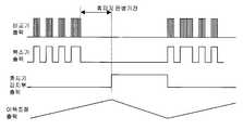
도 4a는 정상신호가 입력되는 경우 이득조절부의 동작 파형도이다.4A is an operation waveform diagram of a gain control unit when a normal signal is input.
도 4b는 노이즈신호가 입력되는 경우 이득조절부의 동작 파형도이다.And FIG. 4B is an operation waveform diagram of a gain control unit when a noise signal is input.
* 도면의 주요부분에 대한 기호의 설명Explanation of Symbols for Main Parts of Drawings
11 : 입력부(input stage) 12 : 초단증폭부 (pre-amp)11: input stage 12: first-stage amplifying unit (pre-amp)
13 : 자동이득조절 증폭기(AGC amp) 14 : 리미트 증폭기(limit amp)13: Automatic gain control amplifier (AGC amp) 14: Limit amplifier (limit amp)
15 : 대역통과필터(Band Pass Filter) 16 : 이득조절부(AGC control)15: band pass filter 16: gain control section (AGC control)
17 : 비교기 (comparator) 18 : 복조기(demodulator)17: comparator 18: demodulator
19 : 슈미트 출력회로부(Schmitt out) 20 : 휴지기 감지부19: Schmitt output circuit part (Schmitt out) 20:
21 : 통상적인 노이즈 신호파형 22 : 리모콘 신호파형21: Typical noise signal waveform 22: Remote control signal waveform
23 : 정상신호의 확대된 신호 구간(버스트 신호구간)23: Extended signal section of normal signal (burst signal section)
25 : 휴지기(gap time)25: gap time
본 발명은 적외선 수신장치에 관한 것으로, 좀 더 구체적으로는 TV나 VCR등의 가전제품에 사용되는 적외선 리모콘이나 기타 적외선 데이터 송신 장치로부터 적외선 신호를 받아서 처리하는 적외선 수신장치에 관한 것이다.BACKGROUND OF THE INVENTION 1. Field of the Invention The present invention relates to an infrared ray receiving apparatus, and more particularly, to an infrared ray receiving apparatus for receiving and processing an infrared ray signal from an infrared remote controller or other infrared data transmitting apparatus used in household appliances such as TVs and VCRs.
통상적으로 쓰이는 종래의 적외선 수신장치의 기술은 대한민국 특허등록번호 제 322520호에 개시되어 있다. 이 등록특허 역시 (주) 에이디텍에 의해 대한민국 특허청에 출원되고 등록된 특허기술이다. 이 기술을 예로 들어 종래의 기술을 설명하기 위해서 도 1 에는 종래의 기술의 도면을 다시 나타내었다.
도 1에 나타낸 종래 기술에 따르면 먼저 포토다이오드가 포함된 입력부(11)가 외부에서 수신된 적외선 입력신호를 감지하여 적외선 신호를 전기신호로 바꾸어 준다. 바뀌어진 전기신호는 미약하므로 초단 증폭기(12)을 통하여 적절한 값으로 증폭된다. 초단증폭부(12)의 목적은 후술하게 될 여러 가지 회로 내에서 미약한 전기신호를 적절히 다룰 수 있을 정도의 크기로 증폭하는 것이다.
초단증폭부(12)로부터 한번 증폭된 신호는 이득이 조절 가능하도록 설계된 자동이득조절증폭기(AGC:Automatic Gain Control Amp)(13)를 통해 이득이 다시 적절히 조절된다. 이러한 이득의 조절은 회로 내부의 특정한 전류나 특정한전압을 조절함으로서 행해지는데 상세한 동작은 첨부된 도면을 참조하여 후술될 것이다.
자동이득조절증폭기(13)를 거친 신호는 최종적으로 리미트(limit)증폭기(14)를 통해 다시 한번 증폭된다. 리미트 증폭기(14)는 본 발명의 적외선 수신장치에 있어서 필수불가결한 구성요소는 아니다. 리미트 증폭기(14)가 없어도 적외선 수신장치의 동작은 정상적으로 이루어 질수 있다. 리미트 증폭기(14)의 출력신호는 다시 대역통과필터(BPF:Band Pass Filter)(15)를 거치면서 적외선 신호의 캐리어(carrier) 주파수 신호를 걸러낸다.
이들 회로들 사이에는 이른바 커플링(coupling) 커패시터라 불려지는 수동소자가 삽입되어 각 증폭기의 출력신호에 포함되어 있거나 포함되어 있을지도 모를 DC 성분을 걸러주기도 하나 편의상 표시를 생략하였다. 대역통과필터(15)의 출력은 이득조절부(16)와 비교기(17)로 입력된다. 이득조절부(16)의 역할은 대역통과필터에서 출력된 신호가 노이즈인지 정상신호(예컨대 리모콘 등에서 발생한)인지의 여부에 따라 자동이득조절증폭기(13)의 이득을 조절할 목적으로 이득조절전류나 이득조절전압을 발생시키는 부분이다.
비교기(17)는 기준으로 설정해 놓은 기준 DC 전압인 Vref(그림에서는 생략되었다)과 대역통과필터의 출력을 비교하는 동작을 하는 회로로 상세한 비교동작은 후술될 것이다. 기준전압 Vref은 비교기(17)가 적절한 비교동작을 통해 원하는 대역통과필터의 출력과 Vref 전압 가운데서 원하는 신호만을 출력시키기 위한 것으로 이 Vref전압은 설계자에 의해 적절히 선택되어 설정된다. 비교기(17)의 출력은 복조기(demodulator)(18)와 연결되어 있고, 복조기(18)의 출력신호는 슈미트 회로부(19)를 통하여 출력된다.A conventional technique of a conventional infrared ray receiving apparatus is disclosed in Korean Patent Registration No. 322520. This registered patent is also a patented technology filed and registered with Korea Intellectual Property Office by ADITECH Co., Ltd. In order to illustrate the prior art using this technique as an example, a diagram of the prior art is again shown in Fig.
According to the prior art shown in FIG. 1, an
The amplified signal from the first
The signal passed through the automatic
Between these circuits passive elements called so-called coupling capacitors are inserted to filter out DC components which may or may not be included in the output signal of each amplifier, but the representation is omitted for convenience. The output of the
The
종래의 기술을 나타낸 도 1에서 포토다이오드로부터의 출력은 여러단의 증폭기를 거친 후 대략 수십 내지는 수백 KHz 전후의 중심주파수를 갖는 대역통과필터(15)로 입력된다. 비교기의 입력중 하나인 Vref 신호는 그 값이 대역통과필터(15) 출력의 평균전압보다 약간 높은 전압으로 결정되어 있다. 비교기(17)는 Vref보다 높은 전압이 대역통과필터(15)에서 들어올 경우 TTL 레벨의 신호로 변환하여 출력한다. 이 출력신호는 다시 복조기에서 캐리어 주파수가 제거되고 신호의 "envelope"라 부르는 부분만 남게되어 신호의 복조가 완성된다.In the conventional technique, the output from the photodiode is input to a band-
한편 외부로부터 적외선 수신장치에 들어오는 입력신호에는 적외선 성분만 있는 것이 아니라 형광등 또는 햇빛 등과 같은 원하지 않는 외란광(外亂光도) 함께 입력되는 것이 보통이다. 이러한 외란광은 설계자가 의도하지 않았던 것들이므로 노이즈 성분이라 간주된다.On the other hand, an input signal coming from the outside to the infrared ray receiving apparatus is not only infrared rays but also unwanted disturbance light such as a fluorescent lamp or sunlight. Such disturbance light is considered to be a noise component because it is not intended by the designer.
본 발명의 중요한 목적 가운데 하나는 바로 이와 같은 노이즈 성분을 후술할 본 발명의 기술을 이용하여 적절히 제한하는 것이다.One of the important objects of the present invention is to adequately limit such a noise component by using the technique of the present invention to be described later.
전술한 이와 같은 노이즈 성분 역시 적외선 수신장치내부의 회로를 통해 최종 출력으로 전달되므로 노이즈에 의해 적외선 수신장치가 오동작할 가능성이 커진다. 적외선 수신장치가 신뢰성이 있는 동작을 하기 위해서는 이와 같은 외부의 노이즈를 제거하거나 적절히 억제하여야 한다.
이를 위해 도 1에 나타낸 종래의 기술에서는 노이즈 제거를 위해 이득조절부(16)와 자동이득조절증폭기(Automatic Gain Controller:AGC)(13)를 이용하는 것이다. 이득조절부(16)로 입력되는 신호가 만약 노이즈일 경우는 자동이득조절증폭기(13)의 이득이 감소하는 방향으로 이득조절부(16)가 동작하여 자동이득조절증폭기에서 노이즈 전달을 억제하고, 입력신호가 노이즈가 아닌 정상적인 신호일 경우는 자동이득조절증폭기(13) 이득이 유지 또는 증가하도록 이득조절부(16)가 동작한다. 이와 같은 동작에 의해 복조기(demodulator)(18)나 최종출력부(19)의 출력신호는 노이즈가 적절히 억제되고 정상적인 신호만을 출력하게 된다.Since the noise component is also transmitted to the final output through the circuit inside the infrared receiver, there is a high possibility that the infrared receiver malfunctions due to noise. In order for the infrared receiver to operate reliably, such external noise must be removed or appropriately suppressed.
To this end, the prior art shown in FIG. 1 uses a
적외선 수신장치 내부로 변조되어 들어온 신호가 노이즈인지 리모콘 등에서 입력되는 정상신호인지 구분하는 방법을 도 2에 나타난 신호 파형들을 참조로 하여 설명한다.
도 2에는 적외선 수신장치로 변조되어 입력되는 노이즈 신호(21), 정상적인 신호(22) 및 정상적인 신호의 확대 파형도를 나타낸 것이다. 노이즈 신호(21)의 실제 크기는 정상적인 신호(22)보다 작지만 도 2에는 설명의 편의상 비슷한 크기로 표현하였다. 정상적인 신호(22)에도 노이즈 신호 성분이 당연 포함되어 있을수 있지만 이 역시 설명의 편의상 정상신호에는 표시되지 않았다. 통상적인 리모콘 신호의 파형(22)은 그림에서 보듯이 노이즈파형과는 확연히 구분된다. 정상적인 리모콘 신호의 경우에는 정상신호 -캐리어 신호에 실린-가 들어오는 버스트(burst)신호 구간과 캐리어 신호가 입력되지 않는 구간, 즉 휴지기(Gap time)가 확연히 차이가 난다. 버스트 신호입력 구간과 휴지기를 비교하면 통상적으로는 휴지기의 구간이 길다. 따라서 버스트 신호입력구간이 전체 신호구간에서 차지하는 비율은 50%가 초과하지 않는다. 그러나 도 2에서 보듯이 노이즈 신호의 경우에는 정상신호의 경우와는 달리 휴지기 구간이 없거나 짧다. 전술한 종래의 특허발명은 적외선 신호와 노이즈신호가 이같이 서로 다른 듀티비(duty ratio)를 갖고 있는 점을 착안한 것이다.
이 종래의 특허발명에 따르면 정상적인 리모콘 신호의 경우에는 신호가 입력되는 동안 자동이득 조절부(16) 내부에 있는 커패시터를 충전시키고, 휴지기동안은 이 커패시터가 방전되도록 이득조절부(16)가 동작하게 된다. 적외선 수신장치에 입력되는 신호가 노이즈인 경우는 휴지기 구간이 짧거나 없어서 이 커패시터는 계속 충전만 할 것이므로 커패시터 양단의 전압은 일정전압을 초과하게 될 것이다. 이 커패시터 양단의 전압을 이용하여 자동이득조절증폭기(13)의 이득을 조절하는데 자동이득조절증폭기는 이 커패시터 양단의 전압이 증가하면 그 이득을 감쇄시키는 방향으로 동작하고, 이 커패시터 전압이 감소하면 그 이득을 증가시키는 방향으로 동작한다. 여기서 커패시터 양단 전압의 증감 방향에 따른 자동이득조절 증폭기 이득의 증감방향은 바뀔 수 있다. 이러한 동작에 따라 노이즈 신호는 자동이득조절증폭기를 거치게 되면서 억제된다. 정상적인 리모콘 신호, 즉 버스트 신호구간과 휴지기가 같이 포함된 구간에서는 전술한 커패시터가 충방전을 되풀이하면서 커패시터 양단의 전압은 일정전압을 초과하지 않게 될 것이다. 따라서 정상적인 신호는 자동이득조절증폭기(13)를 통과하더라도 그 크기가 적절히 유지된다.A method of distinguishing whether a signal modulated into the infrared ray receiving apparatus is a noise or a normal signal inputted from a remote controller or the like will be described with reference to signal waveforms shown in Fig.
2 shows a magnified waveform diagram of the
According to the conventional patented invention, in the case of a normal remote control signal, the
이득조절부(16)의 동작을 요약하면 유입된 신호의 종류에 따라 이득조절부의 커패시터를 충전할 것인가 방전할 것인가를 먼저 판별하고 난 후 다음의 단계로서 충방전을 조절하는 출력신호를 자동이득조절증폭기로 출력하여 증폭기의 이득을 조절한다.To summarize the operation of the
전술한 종래의 기술은 결국 적외선 수신장치에 변조되어 입력된 버스트 신호의 지속구간 대 전체 신호구간의 비율이 50%가 넘지 않으면 정상신호로, 그렇지 않으면 노이즈로 판단하고 이에 따라 자동이득조절증폭기의 이득을 조절하여 노이즈 신호를 억제한다는데 그 기술적인 특징이 있는 것이다.The conventional technique described above determines that the signal is a normal signal if the ratio of the sustain period to the entire signal period of the burst signal modulated and input to the infrared ray receiving apparatus does not exceed 50% To control the noise signal, which is a technical feature.
그러나 이와 같은 종래의 기술에서는 전자식 형광등에서 발생하는 외란광(外亂光)은 일반적인 태양광 노이즈 보다 훨씬 강변조(strongly modulated) 신호된 신호이므로 버스트 신호의 비율이 50% 정도의 수준으로 떨어지게 되어 정상신호의 경우와 비슷한 듀티비를 가진다. 이 같은 특성은 적외선 수신장치회로에서는 노이즈로 인식되는 것이 아니라 정상적인 신호로 인식되는 경우가 있어 적외선 수신장치 회로가 오동작을 일으키는 원인이 된다.However, in this conventional technique, since the disturbance light generated in the electronic fluorescent lamp is a signal that is strongly modulated signal than general solar noise, the ratio of the burst signal drops to about 50% And has a duty ratio similar to that of the signal. Such a characteristic may be recognized as a normal signal instead of being recognized as noise in the infrared receiver circuit, causing the infrared receiver circuit to malfunction.
따라서, 본 발명의 목적은 상술한 제반 문제점을 해결하기 위해 제안된 것으로, 적외선 수신장치로 변조되어 유입되는 신호의 노이즈 여부를 판별할 때 종래의 기술인 버스트 신호 대 휴지기의 비율에 의거하여 자동이득조절증폭기의 이득을 조절하는 것이 아니라 휴지기의 지속시간을 이용하여 유입신호의 노이즈 여부를 판별하도록 하는 적외선 수신장치 장치를 제공하는데 있다.SUMMARY OF THE INVENTION Accordingly, the present invention has been made to solve the above-mentioned problems occurring in the prior art, and it is an object of the present invention to provide an automatic gain control The present invention is to provide an infrared ray receiving apparatus which discriminates the noise of an incoming signal by using a duration of a pausing period instead of adjusting the gain of the amplifier.
본 발명의 또 다른 목적은 이와 같은 이득조절부의 동작제어로 인해 적외선을 수신할 수 있는 거리가 보다 길어진 수신장치를 제공하여 보다 노이즈에 둔감한 적외선 수신장치를 제공하여 본 발명의 수신장치를 내장하고 있을 전자기기의 신뢰성 있는 동작을 보장케 하는데 있다.
It is still another object of the present invention to provide a receiving apparatus having a longer distance for receiving infrared rays due to the operation control of the gain adjusting unit, thereby providing an infrared receiving apparatus more insensitive to noise, Thereby ensuring reliable operation of the electronic device.
본 발명의 회로구성을 나타내는 도 3을 참조로 하여 회로동작을 설명한다. 도 3의 블럭도를 도 1에서 나타난 종래의 기술구성과 비교해보면 피드백구성에 차이가 있음을 알 수 있다.
도 3은 본 발명에 의한 적외선 수신장치의 블럭도를 도시한 것으로, 입력부(11), 제1증폭부(12), 제2증폭부(13), 리미트증폭기(14), 대역통과필터(15), 이득조절부(16), 비교기(17), 복조기(18), 출력부(19) 및 휴지기 감지부(20)로 이루어진다.
입력부(11)는 포토 다이오드가 포함되어 입력된 빛 신호를 전기신호로 변환한다.
제1 증폭부(12)는 상기 변환된 전기신호를 증폭하는 것으로, 초단증폭기라고도 한다.
제2 증폭부(13)는 상기 제1 증폭부(12)의 출력을 입력받고 이득이 조절가능한 것으로, 자동이득조절 증폭기라고도 한다.
리미트 증폭기(14)는 자동이득조절증폭기(13)를 거친 신호를 최종적으로 다시 한번 증폭한다. 본 발명의 적외선 수신장치에 있어서 필수불가결한 구성요소는 아니다.
대역통과필터부(15)는 상기 제2 증폭부 또는 리미트 증폭기(14)의 출력에 포함된 특정한 주파수의 전기신호만을 걸러낸다.
이득조절부(16)는 상기 복조기(18)의 출력이나 상기 비교기(17)의 출력 가운데 하나를 입력받아 신호의 휴지기 구간을 감지하는 휴지기 감지부(20)와 감지된 신호의 길이를 알아내어 이에 포함되어 있는 휴지기의 지속시간이 기 설정된 기준 시간값을 초과하는지의 여부에 따라 상기 자동이득조절증폭기(13)의 이득이 조절할수 있도록 설계된다.
비교기(17)은 기 설정된 기준 DC 전압과 상기 대역통과필터부(15)의 출력을 비교한다.
복조기(18)는 상기 비교기(17)의 출력을 복조한다.
출력부(19)는 상기 복조기(18)의 출력신호를 적외선 수신장치 외부로 출력한다.
휴지기 감지부(20)은 상기 복조기(18)의 출력을 입력받아 신호의 휴지기 구간을 감지한다.
본 발명을 나타내는 도 3에는 종래의 회로와 같거나 유사한 기능을 하는 회로는 편의상 같은 기호를 부여하였음을 유의하여야 한다. 도 3과 도 3의 각 블럭출력 파형을 나타낸 도 4를 같이 참고로 하여 동작을 설명하면 다음과 같다.The circuit operation will be described with reference to Fig. 3 showing the circuit configuration of the present invention. Comparing the block diagram of FIG. 3 with the prior art configuration shown in FIG. 1, it can be seen that the feedback configuration is different.
3 is a block diagram of an infrared receiver according to the present invention. The infrared receiver includes an
The
The
The
The
The band-
The
The
The
The
The idle
It should be noted that in FIG. 3 which represents the present invention, circuits having the same or similar functions as conventional circuits are given the same symbols for convenience. Referring to FIG. 4 showing each block output waveform of FIG. 3 and FIG. 3, the operation will be described as follows.
적외선 수신장치에 입력되는 정상적인 리모콘 신호의 경우(도 4a) 신호의 휴지기가 대략 20ms ~ 25ms인데 반해 태양광 같은 자연광이나 백열등 같은 화이트 노이즈(white noise) 신호인 경우는 휴지기가 거의 없으며, 전자식 형광등, 삼파장 형광등과 같은 경우는 50Hz, 60Hz 등의 주파수를 갖는 신호이기 때문에 변조된 신호의 휴지기 또한 대략 4~5ms 정도를 넘지 않는다.In the case of a normal remote control signal input to the infrared receiving apparatus (Fig. 4A), the pausing period of the signal is approximately 20 ms to 25 ms. In the case of a white noise signal such as natural light such as sunlight or incandescent lamp, In the case of a three-wavelength fluorescent lamp, since the signal has a frequency of 50 Hz, 60 Hz, etc., the resting period of the modulated signal does not exceed about 4 to 5 ms.
필터에서 출력된 신호는 비교기(17)을 거쳐 복조기(18)를 통해 신호의 복조가 이루어진다. 신호의 복조는 반드시 필요하지는 않으므로 복조기(18) 역시 반드시 거치지 않아도 무방하다. 이 경우 휴지기 감지부(20)의 입력은 복조기(18)의 출력과 연결되는 것이 아니라 비교기(17)의 출력과 연결된다. 복조기(18)가 반드시 필요치 않은 이유는 후술될 것이다. 복조된 신호가 휴지기 감지회로부(20)에 입력되면 입력된 신호가 얼마동안의 휴지기, 즉 신호가 얼마동안 "low"인 구간을 가지는가 판별한다. 이 판별은 미리 설정된 소정의 기간보다 휴지기가 짧으면 노이즈로 판단하고, 휴지기가 그 보다 길면 정상적인 리모콘 신호로 판단하여 그에 따라 전술한 것과 같은 방법으로 이득조절부(16)의 충방전 동작을 제어한다.
전술한 바대로 노이즈와 정상적인 리모콘신호는 휴지기의 길이에 차이가 있으므로 판단의 기준이 되는 소정의 기간은 대략 노이즈와 리모콘 신호의 휴지기의 사이의 값으로 설정하면 되는데 대략 이들 휴지기들의 중간값으로 설정하면 무난하다.
예를 들어 리모콘 신호의 휴지기가 20ms이고 노이즈 신호의 휴지기가 4ms라면 판단의 기준이 되는 시간은 12ms로 설정된다. 복조기(18) 출력의 low 구간이 판단의 기준으로 설정된 기준값보다 긴 경우에만 충방전회로부의 커패시터가 방전동작을 하도록 휴지기 감지부(20)를 설계하면 설계자가 의도한 대로 정상적인 충방전 동작이 가능하다.The signal output from the filter is demodulated through the
As described above, since the noise and the normal remote control signal differ in the length of the pausing period, the predetermined period as the determination criterion is set to a value between the noise and the pausing period of the remote control signal. It is safe.
For example, when the pausing period of the remote control signal is 20 ms and the pausing period of the noise signal is 4 ms, the time of the determination reference is set to 12 ms. If the
이러한 기준값 설정은 회로내에서 여러 가지 방법으로 구현 가능하다. 예를 본 발명의 한 실시 예와 같이 휴지기 감지부(20) 내에 커패시터소자를 구성하여 이를 이용, 커패시터의 충방전의 전압의 시정수를 조절하는 방법으로도 설정가능하다. 또한 클럭신호를 이용하여 특정한 클럭수를 설정하는 것으로도 설계자가 원하는 기준 시간값 설정이 가능하다. 전술한 기준값 설정은 여러 가지 설정방법 가운데 예를 든것에 불과할 뿐 여러 가지 변형과 조합이 가능하다.This reference value setting can be implemented in various ways within the circuit. For example, it is also possible to configure a capacitor element in the pausing
복조기(18)의 역할은 전술한 바와 같이 반드시 필요한 것은 아니다. 도 4a 및 도 4b에서 알 수 있듯이 비교기(17)의 출력신호나 복조기(18)의 출력 가운데 어느것이나 휴지기 감지부(20)에 입력되어도 휴지기 감지부(20)의 동작은 같다. 왜냐하면 노이즈와 정상신호를 판별하는 설정된 기준값이 ms(mili-second) 수준으로 결정되어 있어서 캐리어 주파수가 포함된 복조 이전의 신호와 캐리어 주파수가 걸러진 복조 이후의 신호가 휴지기 감지부(20)내에서 같은 신호로 간주되기 때문이다.
심지어 휴지기 감지부(20)의 입력신호는 종래의 기술과 같이 대역통과필터(15)로 부터 오는 것이어도 무방하나 비교기(17)나 복조기(18)로 부터 오는 것이 바람직하다.The role of the
Even the input signal of the
이를 다시 요약하면 비교기(17)의 출력신호를 반드시 복조하지 않아도 버스트 신호 사이 사이에 끼여있는 신호의 소(小)휴지기인 low 구간 - 이 구간을 특별히 소(小)휴지기라 정의한 이유는 노이즈 신호여부를 판단하는 전술한 휴지기와 서로 혼동의 우려가 있기 때문이다 - 은 설정된 기준값보다 훨씬 짧기 때문에 휴지기 감지부(20)의 충방전 특성이 동일하기 때문이다.In summary, the reason why the output signal of the
입력 신호의 휴지기가 얼마나 지속되느냐에 따라 적외선 수신장치에 입력된 신호가 노이즈인지 정상신호인지 판별하여 이득조절부(16) 내부의 커패시터 양단의 전압을 정상적으로 충방전할 것인지, 충전만을 계속할 것인지 결정한다.
이득조절부(16) 내부의 커패시터 양단의 전압이 충전되거나 방전되는 정도는 설계자의 편의와 본 발명의 실시환경에 따라 적절히 변화 가능하다. 이러한 변화는 충전이나 방전에 이용되는 커패시터의 값을 바꾸어 충방전 시정수(time constant)를 조절하여 줌으로써 손쉽게 달성 가능하다.It is determined whether the signal input to the infrared ray receiving apparatus is noise or a normal signal according to how long the rest period of the input signal is maintained to determine whether to normally charge or discharge the voltage across the capacitor inside the
The degree of charging or discharging of the voltage across the capacitor within the
본 발명의 특징은 휴지기가 지속되는 시간이 일정한 기준값을 초과하면 정상적인 신호로, 그렇지 않으면 노이즈로 판단하여 적외선 수신장치 내부의 자동이득조절증폭기의 이득을 임의로 조절할 수 있게 함으로써 적외선 수신장치에 입력되는 노이즈를 억제하고자 하는 것이다.According to an aspect of the present invention, when the duration of the idle period exceeds a predetermined reference value, the gain of the automatic gain control amplifier in the infrared receiver can be arbitrarily adjusted by judging that the signal is a normal signal, .
본 발명으로 인해 적외선 수신장치에 유입되는 노이즈가 적절히 억제되어 적외선 수신장치의 동작 신뢰성이 뚜렷이 좋아지는 효과가 있다.The present invention has an effect that the noise introduced into the infrared ray receiving apparatus is appropriately suppressed and the operation reliability of the infrared ray receiving apparatus is remarkably improved.
본 발명의 여러 실시 예는 전술한 발명의 상세한 설명에서 상술되었으나 본발명의 기술적인 사상을 벗어나지 않으면서 각종 형태의 실시가 가능할 것이므로 본 발명의 청구항의 범위내에서의 모든 변형, 또는 그러한 범위와 동등한 것들은 본 발명에 포함되는 것이고 본 발명의 범위는 명세서에 나타난 실시 예만으로 제한되는 것은 아니다.
While the present invention has been particularly shown and described with reference to exemplary embodiments thereof, it is clearly understood that the same is by way of illustration and example only and is not to be taken as limiting of the scope of the invention as defined by the appended claims. Are included in the present invention and the scope of the present invention is not limited to the embodiments shown in the specification.
Claims (5)
Translated fromKoreanPriority Applications (3)
| Application Number | Priority Date | Filing Date | Title |
|---|---|---|---|
| KR1020030001127AKR100576094B1 (en) | 2003-01-08 | 2003-01-08 | Infrared receiver |
| TW92137623ATWI240501B (en) | 2003-01-08 | 2003-12-31 | Infrared-ray receiver |
| CNB2004100001994ACN1316766C (en) | 2003-01-08 | 2004-01-06 | Infrared receiver |
Applications Claiming Priority (1)
| Application Number | Priority Date | Filing Date | Title |
|---|---|---|---|
| KR1020030001127AKR100576094B1 (en) | 2003-01-08 | 2003-01-08 | Infrared receiver |
Publications (2)
| Publication Number | Publication Date |
|---|---|
| KR20040004030A KR20040004030A (en) | 2004-01-13 |
| KR100576094B1true KR100576094B1 (en) | 2006-05-03 |
Family
ID=37314982
Family Applications (1)
| Application Number | Title | Priority Date | Filing Date |
|---|---|---|---|
| KR1020030001127AExpired - LifetimeKR100576094B1 (en) | 2003-01-08 | 2003-01-08 | Infrared receiver |
Country Status (1)
| Country | Link |
|---|---|
| KR (1) | KR100576094B1 (en) |
Families Citing this family (5)
| Publication number | Priority date | Publication date | Assignee | Title |
|---|---|---|---|---|
| KR100576096B1 (en)* | 2004-10-12 | 2006-05-03 | 주식회사 에이디텍 | Automatic voltage gain circuit for suppressing disturbance light |
| KR100752523B1 (en)* | 2005-12-15 | 2007-08-29 | 주식회사 에이디텍 | Infrared receiver |
| KR100844162B1 (en)* | 2006-10-02 | 2008-07-04 | 주식회사 에이디텍 | Photodiode Connection Circuit |
| KR100795692B1 (en)* | 2006-10-19 | 2008-01-17 | 주식회사 에이디텍 | Optical receiver |
| KR100906712B1 (en)* | 2008-03-04 | 2009-07-07 | 주식회사 네오디바이스 | Noise Infrared Receiver |
- 2003
- 2003-01-08KRKR1020030001127Apatent/KR100576094B1/ennot_activeExpired - Lifetime
Also Published As
| Publication number | Publication date |
|---|---|
| KR20040004030A (en) | 2004-01-13 |
Similar Documents
| Publication | Publication Date | Title |
|---|---|---|
| KR100752523B1 (en) | Infrared receiver | |
| KR100576094B1 (en) | Infrared receiver | |
| TWI455502B (en) | Infrared receiver circuit | |
| KR101044056B1 (en) | Infrared receiver with mode control gain | |
| CN1106719C (en) | data transfer system | |
| JP2003152649A (en) | Optical receiver | |
| KR100575351B1 (en) | Infrared receiver with noise canceling function | |
| CN1316766C (en) | Infrared receiver | |
| CN102355298A (en) | Infrared receiver with digital gain control circuit | |
| KR200179443Y1 (en) | Infrared receiver | |
| JP3305534B2 (en) | Infrared receiver | |
| US7583944B2 (en) | Demodulation and regulation concept for IR receivers | |
| KR100445934B1 (en) | Infra-red receiver | |
| KR101404569B1 (en) | The noise removing circuit of infrared rays receiver | |
| KR100847062B1 (en) | Infrared receiver and method | |
| KR102135332B1 (en) | Infrared receiving device, semiconductor circuit and electronic device including the same | |
| CN100568749C (en) | Discrimination circuit, signal processing circuit, and electronic apparatus | |
| KR20000008682A (en) | Method of preventing a malfunction of a remote control receiver and apparatus thereof | |
| KR101380785B1 (en) | Infrared Signal Receiver of having Gain Hold Function | |
| JP3563667B2 (en) | Signal demodulation circuit and optical signal receiving device using the same | |
| JPH11331076A (en) | Infrared signal processing circuit | |
| KR20040063638A (en) | Control circuit of infrared-ray recceiver | |
| KR19990026445A (en) | Receiver for remote control | |
| JP2004056541A (en) | Remote control light receiver | |
| KR101775937B1 (en) | Improved ir receiver structure |
Legal Events
| Date | Code | Title | Description |
|---|---|---|---|
| A201 | Request for examination | ||
| PA0109 | Patent application | Patent event code:PA01091R01D Comment text:Patent Application Patent event date:20030108 | |
| PA0201 | Request for examination | ||
| AMND | Amendment | ||
| G15R | Request for early publication | ||
| PG1501 | Laying open of application | Comment text:Request for Early Opening Patent event code:PG15011R01I Patent event date:20031222 | |
| E902 | Notification of reason for refusal | ||
| PE0902 | Notice of grounds for rejection | Comment text:Notification of reason for refusal Patent event date:20050627 Patent event code:PE09021S01D | |
| AMND | Amendment | ||
| E601 | Decision to refuse application | ||
| PE0601 | Decision on rejection of patent | Patent event date:20060126 Comment text:Decision to Refuse Application Patent event code:PE06012S01D Patent event date:20050627 Comment text:Notification of reason for refusal Patent event code:PE06011S01I | |
| J201 | Request for trial against refusal decision | ||
| PJ0201 | Trial against decision of rejection | Patent event date:20060224 Comment text:Request for Trial against Decision on Refusal Patent event code:PJ02012R01D Patent event date:20060126 Comment text:Decision to Refuse Application Patent event code:PJ02011S01I Appeal kind category:Appeal against decision to decline refusal Decision date:20060419 Appeal identifier:2006101001664 Request date:20060224 | |
| AMND | Amendment | ||
| PB0901 | Examination by re-examination before a trial | Comment text:Amendment to Specification, etc. Patent event date:20060327 Patent event code:PB09011R02I Comment text:Request for Trial against Decision on Refusal Patent event date:20060224 Patent event code:PB09011R01I Comment text:Amendment to Specification, etc. Patent event date:20050927 Patent event code:PB09011R02I Comment text:Amendment to Specification, etc. Patent event date:20031222 Patent event code:PB09011R02I | |
| B701 | Decision to grant | ||
| PB0701 | Decision of registration after re-examination before a trial | Patent event date:20060419 Comment text:Decision to Grant Registration Patent event code:PB07012S01D Patent event date:20060406 Comment text:Transfer of Trial File for Re-examination before a Trial Patent event code:PB07011S01I | |
| GRNT | Written decision to grant | ||
| PR0701 | Registration of establishment | Comment text:Registration of Establishment Patent event date:20060426 Patent event code:PR07011E01D | |
| PR1002 | Payment of registration fee | Payment date:20060426 End annual number:3 Start annual number:1 | |
| PG1601 | Publication of registration | ||
| PR1001 | Payment of annual fee | Payment date:20090216 Start annual number:4 End annual number:4 | |
| PR1001 | Payment of annual fee | Payment date:20100422 Start annual number:5 End annual number:5 | |
| PR1001 | Payment of annual fee | Payment date:20110706 Start annual number:6 End annual number:6 | |
| PR1001 | Payment of annual fee | Payment date:20120427 Start annual number:7 End annual number:7 | |
| FPAY | Annual fee payment | Payment date:20130426 Year of fee payment:8 | |
| PR1001 | Payment of annual fee | Payment date:20130426 Start annual number:8 End annual number:8 | |
| FPAY | Annual fee payment | Payment date:20140422 Year of fee payment:9 | |
| PR1001 | Payment of annual fee | Payment date:20140422 Start annual number:9 End annual number:9 | |
| FPAY | Annual fee payment | Payment date:20150421 Year of fee payment:10 | |
| PR1001 | Payment of annual fee | Payment date:20150421 Start annual number:10 End annual number:10 | |
| FPAY | Annual fee payment | Payment date:20160222 Year of fee payment:11 | |
| PR1001 | Payment of annual fee | Payment date:20160222 Start annual number:11 End annual number:11 | |
| FPAY | Annual fee payment | Payment date:20170419 Year of fee payment:12 | |
| PR1001 | Payment of annual fee | Payment date:20170419 Start annual number:12 End annual number:12 | |
| FPAY | Annual fee payment | Payment date:20180417 Year of fee payment:13 | |
| PR1001 | Payment of annual fee | Payment date:20180417 Start annual number:13 End annual number:13 | |
| FPAY | Annual fee payment | Payment date:20190423 Year of fee payment:14 | |
| PR1001 | Payment of annual fee | Payment date:20190423 Start annual number:14 End annual number:14 | |
| PR1001 | Payment of annual fee | Payment date:20200423 Start annual number:15 End annual number:15 | |
| PR1001 | Payment of annual fee | Payment date:20210401 Start annual number:16 End annual number:16 | |
| PR1001 | Payment of annual fee | Payment date:20220412 Start annual number:17 End annual number:17 | |
| PC1801 | Expiration of term | Termination date:20230708 Termination category:Expiration of duration |