KR100575657B1 - How to Read Nand Flash - Google Patents
How to Read Nand FlashDownload PDFInfo
- Publication number
- KR100575657B1 KR100575657B1KR1020040086832AKR20040086832AKR100575657B1KR 100575657 B1KR100575657 B1KR 100575657B1KR 1020040086832 AKR1020040086832 AKR 1020040086832AKR 20040086832 AKR20040086832 AKR 20040086832AKR 100575657 B1KR100575657 B1KR 100575657B1
- Authority
- KR
- South Korea
- Prior art keywords
- page
- error
- bit error
- nand flash
- data
- Prior art date
- Legal status (The legal status is an assumption and is not a legal conclusion. Google has not performed a legal analysis and makes no representation as to the accuracy of the status listed.)
- Expired - Fee Related
Links
Images


Classifications
- G—PHYSICS
- G06—COMPUTING OR CALCULATING; COUNTING
- G06F—ELECTRIC DIGITAL DATA PROCESSING
- G06F11/00—Error detection; Error correction; Monitoring
- G06F11/07—Responding to the occurrence of a fault, e.g. fault tolerance
- G06F11/08—Error detection or correction by redundancy in data representation, e.g. by using checking codes
- G—PHYSICS
- G06—COMPUTING OR CALCULATING; COUNTING
- G06F—ELECTRIC DIGITAL DATA PROCESSING
- G06F12/00—Accessing, addressing or allocating within memory systems or architectures
- G06F12/02—Addressing or allocation; Relocation
- G06F12/0223—User address space allocation, e.g. contiguous or non contiguous base addressing
- G06F12/023—Free address space management
- G06F12/0253—Garbage collection, i.e. reclamation of unreferenced memory
- G06F12/0261—Garbage collection, i.e. reclamation of unreferenced memory using reference counting
Landscapes
- Engineering & Computer Science (AREA)
- Theoretical Computer Science (AREA)
- Physics & Mathematics (AREA)
- General Engineering & Computer Science (AREA)
- General Physics & Mathematics (AREA)
- Quality & Reliability (AREA)
- Techniques For Improving Reliability Of Storages (AREA)
- Read Only Memory (AREA)
Abstract
Translated fromKoreanDescription
Translated fromKorean도1은 일반적인 낸드 플래시 구조에 대한 일 예시도.1 is an exemplary diagram of a general NAND flash structure.
도2는 종래 낸드 플래시 읽기 방법에 대한 일 실시예 순서도.Figure 2 is a flow chart of one embodiment of a conventional NAND flash read method.
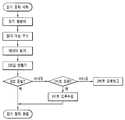
도3은 본 발명에 따른 낸드 플래시 읽기 방법에 대한 일 실시예 순서도.Figure 3 is a flow chart of one embodiment of a NAND flash read method according to the present invention.
본 발명은 낸드(NAND) 플래시 읽기 방법에 관한 것으로, 특히 NAND 플래시에 저장되어 있는 데이터를 읽어오는 과정에서 발생할 수 있는 오류를 최소화하여 NAND 플래시의 읽기 성능을 안정화시킬 수 있는 낸드 플래시 읽기 방법에 관한 것이다.The present invention relates to a NAND flash reading method, and more particularly, to a NAND flash reading method capable of stabilizing read performance of a NAND flash by minimizing an error that may occur during reading data stored in a NAND flash. will be.
최근에 PDA, MP3 플레이어 등에 플래시 메모리가 널리 사용되고 있다. 특히, 저장 매체의 크기가 대용량인 경우에는 NAND 플래시가 널리 사용되고 있는 실정이다.Recently, flash memory is widely used in PDAs, MP3 players and the like. In particular, when the storage medium is large in size, NAND flash is widely used.
플래시 메모리는 노어(NOR) 플래시와 NAND 플래시로 나뉘는데 NOR 플래시는 가격이 비싼 반면 XIP(Execute In Place)가 가능하며 NAND 플래시는 가격이 싼 반면에 XIP 대신 요구 페이징(Demand Paging)을 이용하기 때문에 성능이 떨어지는 경 향이 있다. 여기서, XIP란 플래시 파일 시스템에 저장되어 있는 실행 코드를 램에 적재하지 않고도 실행할 수 있는 기술로서, 램에 대한 메모리 요구량을 줄여주고, 많은 응용 프로그램이 동시에 실행될 수 있도록 해준다.Flash memory is divided into NOR flash and NAND flash. NOR flash is expensive, but it can be Execute In Place (XIP) and NAND flash is cheap, while performance is due to using demand paging instead of XIP. There is a tendency to fall. Here, XIP is a technology that can execute executable code stored in a flash file system without loading it into RAM. It reduces memory requirements for RAM and allows many applications to run simultaneously.
하지만, NAND 플래시에서 사용하는 요구 페이징은 사용자가 필요로 하는 데이터를 NAND 플래시에서 일정 부분 읽어와 SDRAM에 저장하는 기술로서, 사용할 수 있는 SDRAM의 공간이 제한적이기 때문에 NAND 플래시에서 한번 읽어올 수 있는 데이터 양이 많지 않으며 데이터를 읽어오는 시간에 비례하여 시스템 성능이 떨어지게 된다.However, the required paging used by NAND flash is a technology that reads a part of data required by the user from the NAND flash and stores it in SDRAM. The data that can be read once from the NAND flash is limited because the available space of the SDRAM is limited. This is not a large amount and the system performance decreases in proportion to the time to read the data.
도1은 일반적인 NAND 플래시의 구조를 도시한 것으로, 512[Bytes]로 구성된 메인 데이터와 오류 정정 코드(Error Correction Code, 이하 "ECC"라 칭함)가 포함된 16[Bytes]의 스페어 영역으로 구성된다.FIG. 1 shows the structure of a general NAND flash, and is composed of a main area of 512 [Bytes] and a 16 [Bytes] spare area including an Error Correction Code (hereinafter referred to as "ECC"). .
도2는 상기 구조로 이루어진 NAND 플래시에서 데이터를 읽는 방법을 도시한 것으로, 데이터를 읽는 과정에 대해 설명하면 다음과 같다.FIG. 2 illustrates a method of reading data in a NAND flash having the above structure. A process of reading data will be described below.
먼저, 중앙 처리 장치(CPU)에서 NAND 플래시에 저장된 데이터를 읽기 위해 읽기 명령어를 입력하고, 읽고자 하는 NAND 플래시의 주소를 입력한다.First, a CPU inputs a read command to read data stored in a NAND flash, and inputs an address of a NAND flash to be read.
NAND 플래시는 CPU에서 입력한 명령어와 주소를 받아 해당 데이터를 출력하고, CPU는 상기 NAND 플래시에서 출력한 데이터에 오류가 있는지 검출하기 위해 올바른 ECC 값을 생성하여 NAND 플래시에서 출력한 데이터의 ECC 값과 상기 CPU에서 생성된 ECC 값을 비교한다.The NAND flash receives the command and address input from the CPU and outputs the corresponding data, and the CPU generates a correct ECC value to detect whether there is an error in the data output from the NAND flash, and the ECC value of the data output from the NAND flash Compare the ECC value generated in the CPU.
상기 ECC 값 비교 결과, 두 ECC 값이 동일하면 읽기 과정을 종료하고, 두 ECC 값이 동일하지 않으면 CPU에 오류가 있음을 보고한다.As a result of comparing the ECC values, if the two ECC values are the same, the reading process is terminated. If the two ECC values are not the same, the CPU reports an error.
CPU는 상기 두 ECC 값의 비교 결과, NAND 플래시에서 출력한 데이터, 예컨대 데이터의 최소 단위인 512[Bytes]의 페이지에 1비트의 오류가 있으면, NAND 플래시로부터 수신된 ECC 값과 CPU에서 생성된 ECC 값을 이용하여 1비트의 오류를 찾아내서 1비트 오류를 수정한다.As a result of comparing the two ECC values, if the CPU outputs a 1-bit error in a page of data output from the NAND flash, for example, 512 [Bytes] which is the minimum unit of data, the ECC value received from the NAND flash and the ECC generated from the CPU Use the value to find the 1-bit error and correct the 1-bit error.
하지만, NAND 플래시에서 출력한 데이터에 2비트 오류가 있으면, 2비트 오류가 발생했다는 것만 판단할 수 있고, 오류 위치나 오류 값을 찾지 못하기 때문에 CPU로 2비트 오류를 보고하고, 읽기 동작을 다시 수행한다. 재 시도된 읽기 동작에서도 2비트 오류가 발생하면 이를 해결할 방법이 없다.However, if there is a 2-bit error in the data output from the NAND flash, it can only determine that a 2-bit error has occurred, and because it cannot find the error location or error value, it reports the 2-bit error to the CPU and rereads the read operation. To perform. If a 2-bit error occurs even in a retryed read operation, there is no solution.
즉, 종래 NAND 플래시에 저장된 데이터를 읽는 경우 512[Bytes]당 1비트의 오류는 위치를 찾고 오류 값을 고칠 수 있으나, 2비트 오류에 대해서는 해결책이 없었다. 물론, 2비트 오류가 발생할 확률이 낮지만, 점점 대용량의 NAND 플래시를 사용하는 장치가 늘어나면서 읽기 동작도 많아지게 되고, 이에 따라 2비트 이상의 치명적인 오류가 발생할 확률이 높아지게 된다.That is, when reading data stored in a conventional NAND flash, an error of 1 bit per 512 [Bytes] can find a position and correct an error value, but there is no solution for a 2 bit error. Of course, the probability of 2-bit error is low, but as more and more devices using large-capacity NAND flash increase, the read operation increases, thereby increasing the probability of fatal error of 2 bits or more.
따라서, 본 발명은 상기와 같은 종래 문제점을 해결하기 위하여 창출한 것으로, 1비트 오류 발생 시 1비트 오류가 발생한 페이지를 관리하는 기 구성된 오류 페이지 테이블을 업데이트시키고, 1비트 오류 발생 회수가 기 설정된 빈도 기준을 초과하는 페이지가 있으면, 그 빈도 기준을 초과한 페이지에 대한 데이터를 기 설정된 예약 영역에 저장하고, 그 예약 영역에 저장된 페이지에 2비트 오류 발생 시 예약 영역에 저장된 페이지를 이용하여 복원함으로써, 2비트 오류가 발생된 페이지에 대한 오류 복원 능력을 높여 NAND 플래시의 읽기 성능을 향상시킬 수 있는 NAND 플래시 읽기 방법을 제공하는데 그 목적이 있다.Therefore, the present invention was created to solve the above-described conventional problems, and updates a preconfigured error page table for managing a page in which a 1-bit error occurs when a 1-bit error occurs, and the frequency of occurrence of 1-bit error occurrence is preset. If there is a page exceeding the criteria, the data about the page exceeding the frequency criteria is stored in the preset reserved area, and when a 2-bit error occurs in the page stored in the reserved area, it is restored by using the page stored in the reserved area. The purpose of the present invention is to provide a NAND flash read method that can improve the read performance of NAND flash by increasing the error resilience of a page having a 2-bit error.
상기와 같은 목적을 달성하기 위한 본 발명은 중앙 처리 장치(CPU)에서 읽기 명령어와 읽기 주소를 입력하여 낸드(NAND) 플래시로부터 해당 페이지에 대한 데이터를 읽는 제 1단계와; 상기 해당 페이지 데이터에 오류가 있는지 검출하기 위한 올바른 오류 정정 코드(ECC:Error Correction Code) 값을 생성하고, 그 생성된 오류 정정 코드 값와 상기 해당 페이지의 오류 정정 코드 값을 비교하는 제2 단계와; 상기 두 오류 정정 코드 값의 비교 결과, 상기 해당 페이지에 1비트 오류 발생 시 그 발생한 1비트 오류를 수정한 후 1비트 오류가 발생한 페이지를 관리하는 기 구비된 오류 페이지 테이블을 업데이트시키고, 상기 해당 페이지의 1비트 오류 발생 회수가 기 설정된 빈도 기준 회수를 초과한 경우 해당 페이지 데이터를 기 설정된 예약 영역에 저장하는 제3단계와; 상기 두 오류 정정 코드 값의 비교 결과, 상기 해당 페이지에 2비트 오류 발생 시 해당 페이지에 대한 데이터가 상기 예약 영역에 존재하는지 판단하고, 상기 예약 영역에 해당 페이지에 대한 데이터가 존재하면, 그 예약 영역에 저장된 해당 페이지 데이터를 읽고, 상기 제2 단계를 수행하는 제4단계를 포함하여 이루어진 것을 특징으로 한다.The present invention provides a first step of reading data for a corresponding page from a NAND flash by inputting a read command and a read address in a central processing unit (CPU); Generating a correct error correction code (ECC) value for detecting whether there is an error in the corresponding page data, and comparing the generated error correction code value with an error correction code value of the corresponding page; As a result of comparing the two error correction code values, after correcting the 1-bit error occurred when the 1-bit error occurs in the corresponding page, update the provided error page table for managing the page where the 1-bit error occurs, and the corresponding page Storing the corresponding page data in the preset reserved area when the number of occurrences of 1-bit error of the number exceeds a preset frequency reference number; As a result of the comparison between the two error correction code values, if a 2-bit error occurs in the corresponding page, it is determined whether data for the page exists in the reserved area, and if data for the page exists in the reserved area, the reserved area And a fourth step of reading the corresponding page data stored in the second step and performing the second step.
상기와 같은 특징을 갖는 본 발명 NAND 플래시 읽기 방법에 대한 바람직한 실시예를 첨부한 도면을 참고하여 상세히 설명하면 다음과 같다.A preferred embodiment of the NAND flash reading method of the present invention having the above characteristics will be described in detail with reference to the accompanying drawings.
본 발명은 NAND 플래시의 읽기 동작 수행 중 NAND 플래시에서 출력된 페이지에 1비트 오류가 발생한 경우 그 1비트 오류를 복원하는 것 외에 1비트 오류가 자주 발생하는 페이지들에 대한 테이블을 지속적으로 관리하여 향후 2비트 오류 발생 시 그 2비트 오류를 복원하는 것을 그 요지로 한다.According to the present invention, when a 1-bit error occurs on a page output from a NAND flash while performing a read operation of the NAND flash, in addition to restoring the 1-bit error, the present invention continuously manages a table for pages in which a 1-bit error occurs frequently. The key point is to recover the 2-bit error when the 2-bit error occurs.
상기 2비트 오류 발생 시 복원하는 방법은 1비트 오류가 자주 발생하는 페이지를 테이블로 관리하다가 1비트 발생 회수가 기 설정된 빈도 기준 회수를 초과하면 해당 페이지를 NAND 플래시의 일부 영역인 기 설정된 예약 영역에 저장하고, 그 예약 영역에 저장된 해당 페이지가 후에 2비트 오류가 발생하면 예약 영역에 저장된 동일 페이지를 읽어와서 복원하는 방법이다.The method of restoring a 2-bit error occurs by managing a page in which a 1-bit error occurs frequently as a table, and when the number of 1-bit occurrences exceeds a preset frequency reference number, the page is stored in a predetermined reserved area, which is a part of the NAND flash. If a 2 bit error occurs after a corresponding page stored in the reserved area, the same page stored in the reserved area is read and restored.
이러한 본 발명의 성능은 오류 발생 가능성을 예측하는 것과 예약 영역의 크기에 따라 큰 차이를 보일 수 있는데, 상기 두가지 변수에 대한 최적치는 NAND 플래시를 사용하는 시스템의 특성에 따라 실험을 통해 얻을 수 있다.The performance of the present invention may show a big difference depending on the prediction of the possibility of error and the size of the reserved area. The optimum values for the two variables can be obtained through experiments according to the characteristics of the system using the NAND flash.
도3은 본 발명 NAND 플래시 읽기 방법에 대한 일 실시예 순서도를 도시한 것이다. 도시된 바와 같이, CPU에서 읽기 명령어와 읽기 주소를 입력하여 NAND 플래시로부터 해당 페이지에 대한 데이터를 읽는 제1단계와, CPU에서 ECC 값을 생성하고, 그 생성된 ECC 값과 해당 페이지의 ECC 값을 비교하는 제2단계와, 상기 두 ECC 값 비교 결과, 해당 페이지에 1비트 오류 발생 시 1비트 오류를 수정한 후 기 구비된 오류 페이지 테이블을 업데이트시키고, 해당 페이지의 1비트 오류 발생 회수가 기 설정된 빈도 기준 회수를 초과한 경우 해당 페이지 데이터를 기 설정된 예약 영역에 저장하는 제3단계와, 상기 두 ECC 값 비교 결과, 2비트 오류 발생 시 해당 페 이지에 대한 데이터가 기 설정된 예약 영역에 존재하면, 그 예약 영역에 저장된 해당 페이지 데이터를 읽고, 제2단계부터 다시 수행하는 제4단계를 포함하여 이루어진다.Figure 3 illustrates a flowchart of one embodiment of the present invention NAND flash read method. As shown, the first step of reading data for the page from the NAND flash by inputting a read command and a read address in the CPU, generating an ECC value in the CPU, and generating the generated ECC value and the ECC value of the page. In the second step of comparing and comparing the two ECC values, when a 1-bit error occurs on the page, the 1-bit error is corrected, the error page table provided is updated, and the number of 1-bit error occurrences of the corresponding page is preset. If the frequency reference number is exceeded, the third step of storing the page data in the preset reserved area; and as a result of comparing the two ECC values, if the data for the page exists in the preset reserved area when a 2-bit error occurs, And a fourth step of reading the corresponding page data stored in the reserved area and performing it again from the second step.
또한, 상기 2비트 오류가 발생하고, 2비트 오류가 발생한 해당 페이지에 대한 데이터가 예약 영역에 존재하지 않으면, CPU로 2비트 오류를 보고하는 단계를 더 포함하여 이루어진다.The method may further include reporting a 2-bit error to the CPU when the 2-bit error occurs and data for the page in which the 2-bit error occurs does not exist in the reserved area.
그럼, 상기와 같은 단계로 이루어진 본 발명에 대한 동작을 설명하면 다음과 같다.Then, the operation of the present invention made of the above steps will be described.
먼저, 중앙 처리 장치(CPU)에서 NAND 플래시에 저장된 데이터를 읽기 위해 읽기 명령어를 입력하고, 읽고자 하는 NAND 플래시의 주소를 입력한다.First, a CPU inputs a read command to read data stored in a NAND flash, and inputs an address of a NAND flash to be read.
CPU는 상기 입력한 명령어와 주소에 해당하는 해당 페이지 데이터를 NAND 플래시로부터 읽고, 상기 NAND 플래시에서 출력한 해당 페이지 데이터에 오류가 있는지 검출하기 위한 올바른 ECC 값을 생성하여 NAND 플래시에서 출력한 해당 페이지의 ECC 값과 비교한다.The CPU reads the corresponding page data corresponding to the input command and address from the NAND flash, generates a correct ECC value for detecting whether there is an error in the corresponding page data output from the NAND flash, and outputs the corresponding page data output from the NAND flash. Compare with ECC value.
상기 두 ECC 값 비교 결과, 두 ECC 값이 동일하면 해당 페이지에 오류가 없기 때문에 읽기 과정을 종료하고, 두 ECC 값이 동일하지 않으면 CPU에 오류가 있음을 보고한다.As a result of comparing the two ECC values, if the two ECC values are the same, the reading process is terminated because there is no error in the corresponding page. If the two ECC values are not the same, the CPU reports an error.
CPU는 상기 두 ECC 값의 비교 결과, NAND 플래시에서 출력한 해당 페이지에 1비트 오류가 있으면, NAND 플래시로부터 수신된 ECC 값과 CPU에서 생성된 ECC 값을 이용하여 1비트의 오류를 찾아내서 1비트 오류를 수정한다.As a result of comparing the two ECC values, if the corresponding page output from the NAND flash has a 1-bit error, the CPU finds an error of 1 bit by using the ECC value received from the NAND flash and the ECC value generated by the CPU. Correct the error.
상기 해당 페이지의 1비트 오류가 수정되면, 기 구비된 오류 페이지 테이블의 해당 오류 페이지에 대한 정보를 업데이트시킨다. 즉, 상기 오류 페이지 테이블은 1비트 오류가 발생한 페이지에 대한 1비트 오류 발생 회수를 포함하는데, 상기 테이블에 저장된 페이에 대한 1비트 오류가 다시 발생하면, 그 페이지에 대한 오류 발생 회수를 증가시켜 테이블을 업데이트한다. 그리고, 상기 오류 페이지 테이블에 저장된 페이지들의 1비트 오류 발생 회수가 동일할 경우 최근에 발생한 페이지에 가중치를 둬서 관리한다. 이는 NAND 플래시에 데이터가 저장되어 있는 경우 시간적인 유사성이 있어서 최근에 사용한 데이터가 일정 기간 동안 계속 사용될 가능성이 크기 때문이다.When the 1-bit error of the corresponding page is corrected, information on the corresponding error page of the provided error page table is updated. That is, the error page table includes a 1-bit error count for a page in which a 1-bit error occurs. If a 1-bit error for a page stored in the table occurs again, the error page table is increased to increase the error count for the page. Update When the number of 1-bit error occurrences of the pages stored in the error page table is the same, weights are applied to recently generated pages. This is because, when data is stored in NAND flash, there is a similarity in time, so that recently used data is likely to continue to be used for a period of time.
상기 오류 페이지 테이블을 업데이트한 후 1비트 오류가 발생한 해당 페이지의 오류 발생 회수가 기 설정된 빈도 기준을 초과하였는지 판단한다. 상기 판단 결과, NAND 플래시에서 출력한 해당 페이지의 1비트 오류 발생 회수가 빈도 기준을 초과하면, 해당 페이지에 대한 데이터를 기 설정된 예약 영역에 저장한다. 이때, 예약 영역의 크기는 읽기 동작이 페이지 단위로 이루어지기 때문에 페이지 단위의 예약 영역 크기를 두면 되지만, 일반적으로 지우기 동작을 해야 하는 경우 그 기본 단위가 32개의 페이지로 구성된 블록이기 때문에 예약 영역의 크기를 블록 크기로 하는 것이 바람직하다. 그리고, 예약 영역 크기는 정해진 것이 아니라 저장 장치의 용량 크기와 자주 수행하는 동작에 따라 달라질 수 있다는 것은 자명하다.After updating the error page table, it is determined whether the number of error occurrences of the corresponding page where a 1-bit error has occurred exceeds a preset frequency criterion. As a result of the determination, if the number of occurrences of 1-bit error of the page output from the NAND flash exceeds the frequency criterion, the data for the page is stored in the preset reserved area. In this case, the size of the reserved area can be set as the size of the reserved area because the read operation is performed in units of pages, but in general, when the erase operation is required, the size of the reserved area is because the basic unit is a block of 32 pages. Is preferably the block size. And, it is apparent that the reserved area size is not determined but may vary depending on the capacity size of the storage device and frequently performed operations.
반면, 상기 두 ECC 값의 비교 결과, NAND 플래시에서 출력한 해당 페이지에 2비트 오류가 존재하면, 그 해당 페이지와 동일한 페이지 데이터가 예약 영역에 존 재하는지 판단하여 존재하지 않는 경우 기존과 동일하게 CPU로 2비트 오류가 발생했음을 보고한 후 종료하고, 그렇지 않은 경우, 즉, 2비트 오류가 발생한 해당 페이지와 동일한 페이지의 데이터가 예약 영역에 존재하는 경우 그 예약 영역에 저장된 해당 페이지에 대한 데이터를 읽는다.On the other hand, as a result of comparing the two ECC values, if a 2-bit error exists in the corresponding page output from the NAND flash, it is determined whether the same page data as the corresponding page exists in the reserved area, and if it does not exist, the same CPU as before. Reports a 2-bit error and then exits, otherwise it reads the data for that page stored in the reserved area if data on the same page as the page in which the 2-bit error occurred exists in the reserved area. .
상기 예약 영역에 저장된 해당 페이지에 대한 데이터를 읽으면, 읽기 동작이 수행되었기 때문에 CPU에서 해당 페이지의 오류 검출을 위한 올바른 ECC 값을 생성하고, 상기 예약 영역에서 읽은 해당 페이지의 ECC 값과 상기 CPU에서 생성된 ECC 값을 비교하는 과정부터 다시 수행한다.When reading data about the page stored in the reserved area, since the read operation is performed, the CPU generates a correct ECC value for error detection of the page, and generates the ECC value of the page read in the reserved area and the CPU. The process of comparing the ECC values is performed again.
이와 같이 본 발명은 상기 예약 영역에서 읽은 해당 페이지의 ECC 값과 CPU에서 생성된 ECC 값의 비교를 통해 오류를 수정할 수 있기 때문에 NAND 플래시에서 출력한 해당 페이지에 2비트 오류가 발생하더라도 오류를 복원할 수 있는 확률을 높일 수 있는 장점이 있다.As described above, the present invention can correct the error by comparing the ECC value of the corresponding page read from the reserved area with the ECC value generated by the CPU. Therefore, even if a 2-bit error occurs in the corresponding page output from the NAND flash, the error can be restored. There is an advantage that can increase the probability.
또한, 본 발명은 사용 빈도가 낮은 페이지들의 오류 특성을 알기 어렵기 때문에 NAND 플래시에 저장된 전체 페이지에 대한 데이터를 초기화 과정에서 한번씩 읽어서 모든 페이지의 읽기 오류 특성을 알아두는 것이 바람직하다.In addition, the present invention is difficult to know the error characteristics of pages of low use frequency, it is preferable to read the data about the entire page stored in the NAND flash once in the initialization process to know the read error characteristics of all pages.
상기에서 상세히 설명한 바와 같이 본 발명은 1비트 오류 발생 시 1비트 오류가 발생한 페이지를 관리하는 기 구성된 오류 페이지 테이블을 업데이트시키고, 1비트 오류 발생 회수가 기 설정된 빈도 기준을 초과하는 페이지가 있으면, 그 빈도 기준을 초과한 페이지에 대한 데이터를 기 설정된 예약 영역에 저장하고, 그 예 약 영역에 저장된 페이지에 2비트 오류 발생 시 예약 영역에 저장된 페이지를 이용하여 복원함으로써, 2비트 오류가 발생된 페이지에 대한 오류 복원 능력을 높여 NAND 플래시의 읽기 성능을 향상시킬 수 있는 효과가 있다.As described in detail above, the present invention updates a preconfigured error page table that manages a page in which a 1-bit error occurs when a 1-bit error occurs, and if there is a page whose number of occurrences of 1-bit error exceeds a preset frequency criterion, By storing the data for pages exceeding the frequency criteria in the reserved area and restoring the page stored in the reserved area by using the page stored in the reserved area, the page stored in the reserved area can be restored. This can improve the read performance of NAND flash by increasing the error recovery capability.
Claims (4)
Translated fromKoreanPriority Applications (1)
| Application Number | Priority Date | Filing Date | Title |
|---|---|---|---|
| KR1020040086832AKR100575657B1 (en) | 2004-10-28 | 2004-10-28 | How to Read Nand Flash |
Applications Claiming Priority (1)
| Application Number | Priority Date | Filing Date | Title |
|---|---|---|---|
| KR1020040086832AKR100575657B1 (en) | 2004-10-28 | 2004-10-28 | How to Read Nand Flash |
Publications (1)
| Publication Number | Publication Date |
|---|---|
| KR100575657B1true KR100575657B1 (en) | 2006-05-03 |
Family
ID=37181014
Family Applications (1)
| Application Number | Title | Priority Date | Filing Date |
|---|---|---|---|
| KR1020040086832AExpired - Fee RelatedKR100575657B1 (en) | 2004-10-28 | 2004-10-28 | How to Read Nand Flash |
Country Status (1)
| Country | Link |
|---|---|
| KR (1) | KR100575657B1 (en) |
Cited By (5)
| Publication number | Priority date | Publication date | Assignee | Title |
|---|---|---|---|---|
| CN104932951A (en)* | 2015-07-12 | 2015-09-23 | 符方晓 | Data recovery method for ECC not capable of performing error correction in NAND flash memory |
| US9208028B2 (en) | 2012-09-07 | 2015-12-08 | Samsung Electronics Co., Ltd. | Recovery code management method and memory system using same |
| CN105278866A (en)* | 2014-07-18 | 2016-01-27 | 光宝科技股份有限公司 | Solid state storage device and error correction control method thereof |
| US9348708B2 (en) | 2013-02-20 | 2016-05-24 | Samsung Electronics Co., Ltd. | Memory system performing address mapping according to bad page map |
| CN107704338A (en)* | 2017-08-22 | 2018-02-16 | 深圳市硅格半导体股份有限公司 | A kind of data reconstruction method and device of data storage type flash |
Citations (1)
| Publication number | Priority date | Publication date | Assignee | Title |
|---|---|---|---|---|
| JPH0922387A (en)* | 1995-07-07 | 1997-01-21 | Hitachi Ltd | Memory device |
- 2004
- 2004-10-28KRKR1020040086832Apatent/KR100575657B1/ennot_activeExpired - Fee Related
Patent Citations (1)
| Publication number | Priority date | Publication date | Assignee | Title |
|---|---|---|---|---|
| JPH0922387A (en)* | 1995-07-07 | 1997-01-21 | Hitachi Ltd | Memory device |
Cited By (7)
| Publication number | Priority date | Publication date | Assignee | Title |
|---|---|---|---|---|
| US9208028B2 (en) | 2012-09-07 | 2015-12-08 | Samsung Electronics Co., Ltd. | Recovery code management method and memory system using same |
| US9348708B2 (en) | 2013-02-20 | 2016-05-24 | Samsung Electronics Co., Ltd. | Memory system performing address mapping according to bad page map |
| CN105278866A (en)* | 2014-07-18 | 2016-01-27 | 光宝科技股份有限公司 | Solid state storage device and error correction control method thereof |
| CN105278866B (en)* | 2014-07-18 | 2018-03-27 | 光宝科技股份有限公司 | Solid state storage device and error correction control method thereof |
| CN104932951A (en)* | 2015-07-12 | 2015-09-23 | 符方晓 | Data recovery method for ECC not capable of performing error correction in NAND flash memory |
| CN104932951B (en)* | 2015-07-12 | 2017-09-05 | 符方晓 | A data recovery method when ECC cannot be corrected in NAND flash memory |
| CN107704338A (en)* | 2017-08-22 | 2018-02-16 | 深圳市硅格半导体股份有限公司 | A kind of data reconstruction method and device of data storage type flash |
Similar Documents
| Publication | Publication Date | Title |
|---|---|---|
| CN109582217B (en) | Data storage device and method for writing data into memory device | |
| US7765426B2 (en) | Emerging bad block detection | |
| CN104572489B (en) | Wear leveling method and device | |
| JP5658128B2 (en) | System, method, and computer program for probabilistic multilayer error correction in NAND flash memory | |
| US20190278653A1 (en) | Dynamic error handling in a memory system | |
| US9633749B2 (en) | System and method of managing tags associated with read voltages | |
| US7512864B2 (en) | System and method of accessing non-volatile computer memory | |
| US20080301525A1 (en) | Data refresh apparatus and data refresh method | |
| US10489244B2 (en) | Systems and methods for detecting and correcting memory corruptions in software | |
| CN114237984B (en) | Trim data recovery method and system under abnormal power failure and solid state disk | |
| WO2009156870A1 (en) | Method and apparatus for error correction | |
| US20090024787A1 (en) | Data writing method and apparatus | |
| US7613982B2 (en) | Data processing apparatus and method for flash memory | |
| JP2019096281A (en) | Data storage device and associated operating method | |
| US9594629B2 (en) | Data error correction from cached error correction information | |
| KR100575657B1 (en) | How to Read Nand Flash | |
| CN119883943A (en) | Memory system for performing read reclamation | |
| CN120032676A (en) | A method, device and apparatus for determining a voltage offset value of a control voltage threshold | |
| KR20050075533A (en) | Method of demand paging of pda and input reference page information in page |
Legal Events
| Date | Code | Title | Description |
|---|---|---|---|
| A201 | Request for examination | ||
| PA0109 | Patent application | St.27 status event code:A-0-1-A10-A12-nap-PA0109 | |
| PA0201 | Request for examination | St.27 status event code:A-1-2-D10-D11-exm-PA0201 | |
| D13-X000 | Search requested | St.27 status event code:A-1-2-D10-D13-srh-X000 | |
| D14-X000 | Search report completed | St.27 status event code:A-1-2-D10-D14-srh-X000 | |
| E701 | Decision to grant or registration of patent right | ||
| PE0701 | Decision of registration | St.27 status event code:A-1-2-D10-D22-exm-PE0701 | |
| GRNT | Written decision to grant | ||
| PR0701 | Registration of establishment | St.27 status event code:A-2-4-F10-F11-exm-PR0701 | |
| PR1002 | Payment of registration fee | St.27 status event code:A-2-2-U10-U11-oth-PR1002 Fee payment year number:1 | |
| PG1601 | Publication of registration | St.27 status event code:A-4-4-Q10-Q13-nap-PG1601 | |
| PN2301 | Change of applicant | St.27 status event code:A-5-5-R10-R13-asn-PN2301 St.27 status event code:A-5-5-R10-R11-asn-PN2301 | |
| LAPS | Lapse due to unpaid annual fee | ||
| PC1903 | Unpaid annual fee | St.27 status event code:A-4-4-U10-U13-oth-PC1903 Not in force date:20090426 Payment event data comment text:Termination Category : DEFAULT_OF_REGISTRATION_FEE | |
| R18-X000 | Changes to party contact information recorded | St.27 status event code:A-5-5-R10-R18-oth-X000 | |
| R18-X000 | Changes to party contact information recorded | St.27 status event code:A-5-5-R10-R18-oth-X000 | |
| PC1903 | Unpaid annual fee | St.27 status event code:N-4-6-H10-H13-oth-PC1903 Ip right cessation event data comment text:Termination Category : DEFAULT_OF_REGISTRATION_FEE Not in force date:20090426 | |
| PN2301 | Change of applicant | St.27 status event code:A-5-5-R10-R13-asn-PN2301 St.27 status event code:A-5-5-R10-R11-asn-PN2301 | |
| P22-X000 | Classification modified | St.27 status event code:A-4-4-P10-P22-nap-X000 | |
| PN2301 | Change of applicant | St.27 status event code:A-5-5-R10-R13-asn-PN2301 St.27 status event code:A-5-5-R10-R11-asn-PN2301 |