KR100575452B1 - Reflective type liquid crystal display using electrophoretic display and electrophoretic display - Google Patents
Reflective type liquid crystal display using electrophoretic display and electrophoretic displayDownload PDFInfo
- Publication number
- KR100575452B1 KR100575452B1KR1019990041434AKR19990041434AKR100575452B1KR 100575452 B1KR100575452 B1KR 100575452B1KR 1019990041434 AKR1019990041434 AKR 1019990041434AKR 19990041434 AKR19990041434 AKR 19990041434AKR 100575452 B1KR100575452 B1KR 100575452B1
- Authority
- KR
- South Korea
- Prior art keywords
- electrophoretic
- electrode
- lower plate
- liquid crystal
- substrate
- Prior art date
- Legal status (The legal status is an assumption and is not a legal conclusion. Google has not performed a legal analysis and makes no representation as to the accuracy of the status listed.)
- Expired - Fee Related
Links
Images


Classifications
- G—PHYSICS
- G02—OPTICS
- G02F—OPTICAL DEVICES OR ARRANGEMENTS FOR THE CONTROL OF LIGHT BY MODIFICATION OF THE OPTICAL PROPERTIES OF THE MEDIA OF THE ELEMENTS INVOLVED THEREIN; NON-LINEAR OPTICS; FREQUENCY-CHANGING OF LIGHT; OPTICAL LOGIC ELEMENTS; OPTICAL ANALOGUE/DIGITAL CONVERTERS
- G02F1/00—Devices or arrangements for the control of the intensity, colour, phase, polarisation or direction of light arriving from an independent light source, e.g. switching, gating or modulating; Non-linear optics
- G02F1/01—Devices or arrangements for the control of the intensity, colour, phase, polarisation or direction of light arriving from an independent light source, e.g. switching, gating or modulating; Non-linear optics for the control of the intensity, phase, polarisation or colour
- G02F1/165—Devices or arrangements for the control of the intensity, colour, phase, polarisation or direction of light arriving from an independent light source, e.g. switching, gating or modulating; Non-linear optics for the control of the intensity, phase, polarisation or colour based on translational movement of particles in a fluid under the influence of an applied field
- G02F1/166—Devices or arrangements for the control of the intensity, colour, phase, polarisation or direction of light arriving from an independent light source, e.g. switching, gating or modulating; Non-linear optics for the control of the intensity, phase, polarisation or colour based on translational movement of particles in a fluid under the influence of an applied field characterised by the electro-optical or magneto-optical effect
- G02F1/167—Devices or arrangements for the control of the intensity, colour, phase, polarisation or direction of light arriving from an independent light source, e.g. switching, gating or modulating; Non-linear optics for the control of the intensity, phase, polarisation or colour based on translational movement of particles in a fluid under the influence of an applied field characterised by the electro-optical or magneto-optical effect by electrophoresis
- G—PHYSICS
- G02—OPTICS
- G02F—OPTICAL DEVICES OR ARRANGEMENTS FOR THE CONTROL OF LIGHT BY MODIFICATION OF THE OPTICAL PROPERTIES OF THE MEDIA OF THE ELEMENTS INVOLVED THEREIN; NON-LINEAR OPTICS; FREQUENCY-CHANGING OF LIGHT; OPTICAL LOGIC ELEMENTS; OPTICAL ANALOGUE/DIGITAL CONVERTERS
- G02F1/00—Devices or arrangements for the control of the intensity, colour, phase, polarisation or direction of light arriving from an independent light source, e.g. switching, gating or modulating; Non-linear optics
- G02F1/01—Devices or arrangements for the control of the intensity, colour, phase, polarisation or direction of light arriving from an independent light source, e.g. switching, gating or modulating; Non-linear optics for the control of the intensity, phase, polarisation or colour
- G02F1/13—Devices or arrangements for the control of the intensity, colour, phase, polarisation or direction of light arriving from an independent light source, e.g. switching, gating or modulating; Non-linear optics for the control of the intensity, phase, polarisation or colour based on liquid crystals, e.g. single liquid crystal display cells
- G02F1/133—Constructional arrangements; Operation of liquid crystal cells; Circuit arrangements
- G02F1/1333—Constructional arrangements; Manufacturing methods
- G02F1/1335—Structural association of cells with optical devices, e.g. polarisers or reflectors
- G02F1/133553—Reflecting elements
- G02F1/133555—Transflectors
- G—PHYSICS
- G02—OPTICS
- G02F—OPTICAL DEVICES OR ARRANGEMENTS FOR THE CONTROL OF LIGHT BY MODIFICATION OF THE OPTICAL PROPERTIES OF THE MEDIA OF THE ELEMENTS INVOLVED THEREIN; NON-LINEAR OPTICS; FREQUENCY-CHANGING OF LIGHT; OPTICAL LOGIC ELEMENTS; OPTICAL ANALOGUE/DIGITAL CONVERTERS
- G02F1/00—Devices or arrangements for the control of the intensity, colour, phase, polarisation or direction of light arriving from an independent light source, e.g. switching, gating or modulating; Non-linear optics
- G02F1/01—Devices or arrangements for the control of the intensity, colour, phase, polarisation or direction of light arriving from an independent light source, e.g. switching, gating or modulating; Non-linear optics for the control of the intensity, phase, polarisation or colour
- G02F1/165—Devices or arrangements for the control of the intensity, colour, phase, polarisation or direction of light arriving from an independent light source, e.g. switching, gating or modulating; Non-linear optics for the control of the intensity, phase, polarisation or colour based on translational movement of particles in a fluid under the influence of an applied field
- G02F1/1675—Constructional details
- G02F1/1677—Structural association of cells with optical devices, e.g. reflectors or illuminating devices
- G—PHYSICS
- G02—OPTICS
- G02F—OPTICAL DEVICES OR ARRANGEMENTS FOR THE CONTROL OF LIGHT BY MODIFICATION OF THE OPTICAL PROPERTIES OF THE MEDIA OF THE ELEMENTS INVOLVED THEREIN; NON-LINEAR OPTICS; FREQUENCY-CHANGING OF LIGHT; OPTICAL LOGIC ELEMENTS; OPTICAL ANALOGUE/DIGITAL CONVERTERS
- G02F2201/00—Constructional arrangements not provided for in groups G02F1/00 - G02F7/00
- G02F2201/44—Arrangements combining different electro-active layers, e.g. electrochromic, liquid crystal or electroluminescent layers
- G—PHYSICS
- G02—OPTICS
- G02F—OPTICAL DEVICES OR ARRANGEMENTS FOR THE CONTROL OF LIGHT BY MODIFICATION OF THE OPTICAL PROPERTIES OF THE MEDIA OF THE ELEMENTS INVOLVED THEREIN; NON-LINEAR OPTICS; FREQUENCY-CHANGING OF LIGHT; OPTICAL LOGIC ELEMENTS; OPTICAL ANALOGUE/DIGITAL CONVERTERS
- G02F2203/00—Function characteristic
- G02F2203/62—Switchable arrangements whereby the element being usually not switchable
Landscapes
- Physics & Mathematics (AREA)
- Nonlinear Science (AREA)
- Optics & Photonics (AREA)
- Chemical & Material Sciences (AREA)
- General Physics & Mathematics (AREA)
- Chemical Kinetics & Catalysis (AREA)
- Electrochemistry (AREA)
- Molecular Biology (AREA)
- Life Sciences & Earth Sciences (AREA)
- Health & Medical Sciences (AREA)
- Mathematical Physics (AREA)
- Crystallography & Structural Chemistry (AREA)
- Electrochromic Elements, Electrophoresis, Or Variable Reflection Or Absorption Elements (AREA)
- Liquid Crystal (AREA)
Abstract
Translated fromKoreanDescription
Translated fromKorean도 1은 백라이트에서 나온 빛의 각 층별 투과도를 도식적으로 나타낸 그래프.1 is a graph showing the transmittance of each layer of light emitted from the backlight.
도 2는 종래의 반사형 액정 표시장치의 단면을 도시한 단면도.2 is a cross-sectional view showing a cross section of a conventional reflective liquid crystal display device;
도 3은 종래의 반사/투과형 액정 표시장치의 한 화소부에 해당하는 단면을 도시한 단면도.3 is a cross-sectional view showing a cross section corresponding to one pixel portion of a conventional reflective / transmissive liquid crystal display device;
도 4a는 전기영동 셀의 전압 무인가시 단면을 도시한 단면도.Figure 4a is a cross-sectional view showing a cross section when no voltage is applied to the electrophoretic cell.
도 4b는 전기영동 셀의 전압 인가시 단면을 도시한 단면도.Figure 4b is a cross-sectional view showing a cross section when applying the voltage of the electrophoretic cell.
도 5는 본 발명의 실시예에 따른 전기영동 디스플레이의 단면을 도시한 단면도.Figure 5 is a cross-sectional view showing a cross section of the electrophoretic display according to an embodiment of the present invention.
도 6a는 본 발명의 실시예에 따른 전기영동 디스플레이에 순방향 전압 인가에 따른 동작을 설명한 단면도.Figure 6a is a cross-sectional view illustrating the operation of applying the forward voltage to the electrophoretic display according to an embodiment of the present invention.
도 6b는 본 발명의 실시예에 따른 전기영동 디스플레이에 역방향 전압 인가에 따른 동작을 설명한 단면도.Figure 6b is a cross-sectional view illustrating the operation according to the reverse voltage applied to the electrophoretic display according to an embodiment of the present invention.
도 7은 본 발명의 실시예에 따른 전기영동 디스플레이의 다른 예의 단면을 도시한 단면도.7 is a cross-sectional view showing a cross section of another example of an electrophoretic display according to an embodiment of the present invention.
도 8은 본 발명의 실시예에 따른 전기영동 디스플레를 반사투과형 액정 표시장치에 적용한 단면을 도시한 단면도.FIG. 8 is a cross-sectional view of a cross-section of an electrophoretic display according to an exemplary embodiment of the present invention to a transflective liquid crystal display. FIG.
〈도면의 주요부분에 대한 부호의 설명〉<Explanation of symbols for main parts of drawing>
50 : 투명전극 52 : 하판 50
54 : 집전전극 54a : 보조 집전전극 54
56 : 상판 58 : 용매 56: top 58: solvent
60 : 염료입자 70 : 백라이트 60: dye particle 70: backlight
200 : 전기영동 셀 400 : 화소전극200: electrophoretic cell 400: pixel electrode
402 : 박막 트랜지스터 기판 404 : 컬러필터층402: thin film transistor substrate 404: color filter layer
406 : 공통전극 408 : 컬러필터 기판406: common electrode 408: color filter substrate
410 : 액정층410 liquid crystal layer
본 발명은 액정 표시장치에 관한 것으로서, 더 상세하게는, 고 개구율 및 고 반사효율을 갖는 반사 및 투과 겸용의 반사투과(transflective)형 액정표시 장치에 관한 것이다.BACKGROUND OF THE
최근 정보화 사회로 시대가 급진전함에 따라, 대량의 정보를 처리하고 이를 표시하는 디스플레이(display)분야가 발전하고 있다.Recently, as the information society has progressed rapidly, a display field for processing and displaying a large amount of information has been developed.
근대까지 브라운관(cathode-ray tube ; CRT)이 표시장치의 주류를 이루고 발전을 거듭해 오고 있다.Until modern times, cathode ray tube (CRT) has become the mainstream of display devices and has been developing.
그러나, 최근 들어 박형화, 경량화, 저소비전력화 등의 시대상에 부응하기 위해 평판 표시장치(flat panel display)의 필요성이 대두되었다.However, in recent years, the need for a flat panel display has emerged in order to meet the times of thinning, weight reduction, and low power consumption.
이에 따라 색 재현성이 우수하고 박형인 박막 트랜지스터형 액정표시소자(Thin film transistor-liquid crystal display device ; 이하 TFT-LCD라 한다)가 개발되었다.Accordingly, a thin film transistor-liquid crystal display device (hereinafter referred to as TFT-LCD) having excellent color reproducibility has been developed.
TFT-LCD의 동작을 살펴보면, 박막 트랜지스터에 의해 임의의 화소(pixel)가 스위칭 되면, 스위칭된 임의의 화소는 하부광원의 빛을 투과할 수 있게 한다.Looking at the operation of the TFT-LCD, if any pixel is switched by the thin film transistor, the switched arbitrary pixel can transmit the light of the lower light source.
상기 스위칭 소자는 반도체층을 비정질 실리콘으로 형성한, 비정질 실리콘 박막 트랜지스터(amorphous silicon thin film transistor ; a-Si:H TFT)가 주류를 이루고 있다. 이는 비정질 실리콘 박막이 저가의 유리기판과 같은 대형 절연기판 상에 저온에서 형성하는 것이 가능하기 때문이다.The switching element is mainly composed of an amorphous silicon thin film transistor (a-Si: H TFT) in which a semiconductor layer is formed of amorphous silicon. This is because the amorphous silicon thin film can be formed at a low temperature on a large insulating substrate such as a low-cost glass substrate.
일반적으로 사용되는 TFT-LCD는 패널의 하부에 위치한 백라이트라는 광원의 빛에 의해 영상을 표현하는 방식을 써왔다.Commonly used TFT-LCDs have used a method of representing an image by the light of a light source called a backlight located under the panel.
그러나, TFT-LCD는 백라이트에 의해 입사된 빛의 3∼8%만 투과하는 매우 비효율적인 광 변조기이다.However, TFT-LCDs are very inefficient light modulators that transmit only 3-8% of the light incident by the backlight.
두 장의 편광의 투과도는 45%, 하판과 상판의 유리 두 장의 투과도는 94%, TFT어레이 및 화소의 투과도는 약 65%, 컬러필터 외의 투과도는 27%라고 가정하면 TFT-LCD의 광 투과도는 약 7.4%이다.The light transmittance of the TFT-LCD is about assuming that the transmittance of the two polarized light is 45%, the transmittance of the two glass plates of the lower plate and the upper plate is 94%, the transmittance of the TFT array and pixel is about 65%, and the transmittance other than the color filter is 27%. 7.4%.
도 1은 백라이트에서 나온 빛의 각 층별 투과도를 도식적으로 나타낸 도면이다.1 is a diagram schematically illustrating transmittance of each layer of light emitted from a backlight.
상술한 바와 같이 실제로 TFT-LCD를 통해 보는 빛의 양은 백라이트에서 생성된 광의 약 7%정도이므로, 고 휘도의 TFT-LCD에서는 백라이트의 밝기가 밝아야 하고, 상기 백라이트에 의한 전력 소모가 크다.As described above, since the amount of light actually seen through the TFT-LCD is about 7% of the light generated in the backlight, the brightness of the backlight should be bright in the high brightness TFT-LCD, and the power consumption by the backlight is large.
따라서, 충분한 백라이트의 전원 공급을 위해서는 전원 공급 장치의 용량을 크게 하여, 무게가 많이 나가는 배터리(battery)를 사용해 왔다. 그러나 이 또한 장시간 사용할 수 없었다.Therefore, in order to supply sufficient backlight power, a battery having a large weight has been used by increasing the capacity of the power supply device. However, this too could not be used for a long time.
상술한 문제점을 해결하기 위해 최근에 백라이트광을 사용하지 않는 반사형 TFT-LCD가 연구되었다. 이는 자연광을 이용하여 동작하므로, 백라이트가 소모하는 전력량을 배제할 수 있는 효과가 있기 때문에, 장시간 휴대상태에서 사용이 가능하고, 한 화소부 전체가 개구부가 되기 때문에 개구율 또한 기존의 백라이트형 TFT-LCD보다 우수하다.In order to solve the above problem, a reflective TFT-LCD which does not use backlight light has recently been studied. Since it operates by using natural light, it has the effect of eliminating the amount of power consumed by the backlight, so that it can be used in a portable state for a long time, and since the entire pixel portion becomes an opening, the aperture ratio is also conventional backlight type TFT-LCD. Better than
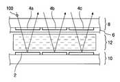
즉, 반사형 TFT-LCD의 단면을 도시한 도 2를 참조하여 설명하면 다음과 같다.That is, the following description will be made with reference to FIG. 2, which shows a cross section of the reflective TFT-LCD.
도 2에 도시된 도면에서와 같이 일반적인 반사형 TFT-LCD는 스위칭소자(미도시)와 상기 스위칭 소자와 각각 접촉하는 반사전극(2)이 형성된 하판(10)과 적, 녹, 청의 색을 띤 컬러필터층(4a, 4b, 4c) 및 상기 컬러필터층(4a, 4b, 4c)을 덮는 공통전극(6)이 형성된 상판(8)과 상기 상판(8)과 하판(10) 사이에 형성된 액정층(12)으로 구성된다.As shown in FIG. 2, a typical reflective TFT-LCD has a red, green, and blue color with a
상기 반사형 TFT-LCD의 동작은 외부광(100)이 상기 상판(8)을 통해 상기 반사전극(2)으로 입사되고, 입사된 외부광(100)은 상기 반사전극(2)에 반사되어 상판(8)을 통해 다시 외부로 방출된다.In the operation of the reflective TFT-LCD, the
이 때, 스위칭 소자를 통해 상기 반사전극(2)에 소정의 신호가 인가되면, 상기 반사전극(2) 상부 상기 액정층(12)은 상이 변하게 되고, 상기 컬러필터층(4a, 4b, 4c)에 의해 반사전극(2)에 의해 반사된 반사광은 착색되어 영상으로 표시되게 된다.At this time, when a predetermined signal is applied to the
상술한 바와 같은 반사형 TFT-LCD는 백라이트와 같은 내부적인 광원을 사용하지 않고, 자연의 빛 내지는 외부의 인조 광원을 사용하여 구동하기 때문에 장시간 사용이 가능하다.The reflective TFT-LCD as described above can be used for a long time because it is driven by using natural light or an external artificial light source without using an internal light source such as a backlight.
즉, 반사형 TFT-LCD는 외부의 자연광을 상기 반사 전극(2)에 반사시켜, 반사된 빛을 이용하는 구조로 되어 있다.In other words, the reflective TFT-LCD reflects external natural light to the
그러나, 자연광 또는 인조 광원이 항상 존재하는 것은 아니다. 즉, 상기 반사형 TFT-LCD는 자연광이 존재하는 낮이나, 외부 인조광이 존재하는 사무실 및 건물 내부에서는 사용이 가능할지 모르나, 자연광이 존재하지 않는 야간에는 상기 반사형 TFT-LCD를 사용할 수 없게 된다.However, natural or artificial light sources do not always exist. That is, the reflective TFT-LCD may be used in the daytime where natural light is present or inside an office and a building where external artificial light exists, but the reflective TFT-LCD cannot be used at night when natural light does not exist. do.
따라서, 상기의 문제점을 해결하기 위해 반사형 TFT-LCD와 투과형 TFT-LCD의 장점을 수용하면서, 주/야간 동시에 사용할 수 있는 액정 표시장치(투과/반사형 액정 표시장치)가 연구/개발되었다.Accordingly, in order to solve the above problems, a liquid crystal display (transmission / reflection type liquid crystal display) that can be used simultaneously and day and night while accepting the advantages of the reflective TFT-LCD and the transmissive TFT-LCD has been researched and developed.
도 3은 일반적인 투과/반사형 액정 표시장치의 구성을 도시한 단면도로써, 그 구성과 동작을 상술하면 다음과 같다.3 is a cross-sectional view showing a configuration of a general transmissive / reflective liquid crystal display device.
도 3에 도시한 바와 같이, 하판(18)에는 스위칭 소자(미도시)와 화소전극(14)과 반사전극(2)이 위치하고, 상기 하판(18) 상부에는 컬러필터(104)가 형성된 상판(22)이 위치하고 있다.As shown in FIG. 3, a switching element (not shown), a
그리고, 상기 하판(18)과 상기 상판(22)에 개재된 형태로 액정층(20)이 위치하고 있다. 또한, 상기 하판(18) 하부에는 백라이트(16)가 위치하고 있다.In addition, the
상기 하판(18) 상부에 형성된 반사전극(2)은 외부광(110)을 반사할 수 있도록 반사율이 우수한 도전물질이 주로 쓰이며, 실질적으로 불투명한 금속이 사용된다.The
그리고, 상기 반사전극(2) 내부에는 평면적으로 투과홀(hole : A)이 존재한다.In addition, a transparent hole (A) exists in the plane of the
즉, 상기 투과홀(A)이 형성된 곳에 화소전극(14)이 위치하여 상기 백라이트(16)로부터 형성된 백라이트광(112)을 투과시키는 역할을 하게 된다.That is, the
상술한 내용을 참조하여 본 발명에 따른 반사투과형 TFT-LCD의 작동을 설명하면, 반사모드에서는 외부 즉, 상판(22)을 통해 입사된 외부광(110)을 상기 반사전극(2)이 상판(22)으로 다시 반사시키는 역할을 하게된다.Referring to the above description, the operation of the reflective transmissive TFT-LCD according to the present invention will be described. In the reflective mode, the
이 때, 스위칭 소자(미도시)로부터 상기 반사전극(2)이 신호를 인가받으면 상기 액정층(20)의 상변화가 일어나게 되고, 이에 따라 재 반사되는 광량의 변화가 있게 되어 상기 광량의 변화에 따라 상기 상판에 형성된 컬러필터(104)에 의해 착색되는 색의 변화에 따라 상기 반사전극(2)에 인가된 신호는 화상으로 표현된다.In this case, when the
그리고, 투과모드에서는 상기 백라이트(16)에서 생성된 빛(112)이 상기 반사전극(2) 내부에 형성된 투과홀(A)에 위치하는 화소전극(14)을 통해 상판(226)으로 투과되게 되는 것이다.In the transmission mode, the light 112 generated by the
이 때, 상기 반사모드와 마찬가지로 상기 스위칭 소자의 작용에 의해 상기 화소전극(14)에 신호가 인가되면, 상기 액정층(20)의 상이 변화되게 되고, 이 때 백라이트(16)에서 방출되어 액정층을 투과한 빛(112)은 상기 상판(22)에 형성된 컬러필터(104)에 의해 착색되어 컬러화면으로 표시된다.At this time, when a signal is applied to the
상술한 바와 같이, 본 발명의 실시예에 따른 반사투과형 TFT-LCD는 반사모드와 투과모드를 겸비하고 있으므로, 주/야간이나 장소에 구애(拘碍)받지 않고 사용할 수 있는 장점이 있다.As described above, since the reflection type TFT-LCD according to the embodiment of the present invention has a reflection mode and a transmission mode, there is an advantage that it can be used regardless of day / night or place.
한편, 최근들어 전기영동 현상을 이용한 광 셔터(shutter) 현상을 이용한 화상 표시장치가 연구/개발되고 있다.On the other hand, an image display device using an optical shutter phenomenon using an electrophoretic phenomenon has recently been researched and developed.
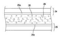
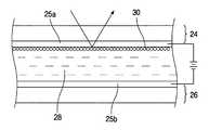
도 4a 내지 도 4b는 전기 영동(electrophoretic ; EP)방식을 이용한 전기영동 표시장치(electrophoretic display ; EPD)의 개략적인 구조의 단면을 도시한 단면도로써, 광 셔터 현상을 이용한 전형적인 예라 할 수 있다.4A to 4B are cross-sectional views illustrating schematic structures of an electrophoretic display (EPD) using an electrophoretic (EP) method, which is a typical example using an optical shutter phenomenon.
상기 EPD의 구성을 살펴보면 다음과 같다.Looking at the configuration of the EPD as follows.
이하 설명될 내용은 개략적인 구조에 관한 것이고, 그 원리에 관해서는 본 발명의 실시예에서 상세히 설명할 것이다.The following description relates to a schematic structure, the principle of which will be described in detail in the embodiments of the present invention.
먼저, 도 4a에 도시된 도면에서와 같이, EPD의 구성은 전극(25)이 형성된 하판(26)과 전극(25)이 형성된 상판(24)으로 구성되며, 상기 상판(24)과 하판(26)에 각각 형성된 전극(25a, 25b)은 서로 마주보고 있다.First, as shown in FIG. 4A, the configuration of the EPD includes a
그리고, 상기 상판(24)과 하판(26) 사이에는 소정의 액체(28)와 상기 액체(28) 내에 전하를 띤 입자(도전 입자)가 분산(dispersion)되어 있다. 상술한 EPD의 구성에서 상기 도 4a에 도시된 도면은 상기 상판(24)과 하판(26)에 각각 형성된 전극(25)에 전압을 인가하지 않은 상태이다.Further, a
도 4b는 상기 상판(24)과 하판(26)에 각각 형성된 전극(25)에 직류전압을 인가했을 때를 도시한 도면으로써, 상기 액체(28)내에 존재하는 대전(帶電)된 입자(30)는 그 극성과 반대되는 극성을 띤 전극(25)으로 이동하게 된다. 또한, 상기 대전된 입자(30)의 극성을 바꾸면 반대방향으로 모이게 할 수 있을 것이다.FIG. 4B is a diagram showing a case where a DC voltage is applied to the
상술한 EPD는 일반적으로 사용되는 투과형 TFT-LCD의 백라이트와 액정 셀 중간에 위치하며, 상기 EPD에 직류전압을 인가하지 않을 경우 백라이트 광에 의한 투과형 TFT-LCD로 사용이 가능하고, 상기 EPD에 직류전압을 인가하면 대전된 입자(30)들이 한 쪽 방향으로 정렬하게 되고, 상기 정렬된 대전 입자(30)가 반사판의 역할을 하게되어 반사형 TFT-LCD로 동작하게 된다.The above-mentioned EPD is located in the middle of the backlight and the liquid crystal cell of a commonly used transmissive TFT-LCD, and can be used as a transmissive TFT-LCD by backlight light when a direct current voltage is not applied to the EPD. When a voltage is applied, the charged
상술한 바와 같은 종래의 반사/투과형 TFT-LCD는 반사형과 투과형모드에서 동작이 가능하기 때문에 저소비전력으로 장시간 사용할 수 있는 장점이 있다.The conventional reflective / transmissive TFT-LCD as described above has the advantage of being able to operate for a long time with low power consumption because it can operate in the reflective and transmissive modes.
그러나, 반사전극과 투과전극이 동시에 형성된 하판의 구조를 가지는 반사/투과형 TFT-LCD의 경우에는 각각 반사형 또는 투과형의 단독으로 사용되는 TFT-LCD의 경우와 비교해서 광 이용 효율이 현저히 감소되는 단점을 가지고 있다.However, in the case of the reflective / transmissive TFT-LCD having the structure of the bottom plate on which the reflective electrode and the transmissive electrode are formed at the same time, the light utilization efficiency is significantly reduced compared to the case of the TFT-LCD which is used alone or in the reflection type. Have
또한, 기존 EPD 기술을 이용한 화상 표시장치는 화소(pixel)화를 위한 기술적인 어려움과 함께, 액정 표시장치에 비해 상대적으로 느린 응답속도와 높은 동작전압을 가지고 있는 단점이 있다.In addition, the image display device using the existing EPD technology has a disadvantage in that it has a relatively slow response speed and a high operating voltage as compared to the liquid crystal display device, along with technical difficulties for pixelization.
상술한 종래의 반사/투과형 액정 표시장치의 문제점을 해결하기 위해 본 발명에서는 EPD 기술을 이용한 액정 표시장치에서 광 효율을 극대화 하는데 그 목적이 있다.
In order to solve the problems of the conventional reflective / transmissive liquid crystal display, the present invention has an object to maximize light efficiency in a liquid crystal display using EPD technology.
상기와 같은 목적을 달성하기 위해 본 발명에서는 일 극성의 전압이 인가되는 투명 도전전극이 전면에 형성된 하판과; 타 극성의 전압이 인가되고 집전전극이 가장자리에 형성된 상판과; 상기 상판과 하판 사이에 형성되고, 내부에 다수개의 대전(帶電)된 전기영동 염료입자를 포함하고, 상기 염료입자와 반응하지 않는 용매(溶媒)을 포함하는 전기영동 셀과; 상기 전기영동 셀의 하부에 위치한 백라이트를 포함하는 전기영동 디스플레이을 제공한다.In order to achieve the above object, the present invention provides a transparent conductive electrode to which a voltage of one polarity is applied; An upper plate to which a voltage of a different polarity is applied and a current collecting electrode is formed at an edge thereof; An electrophoretic cell formed between the upper plate and the lower plate and including a plurality of charged electrophoretic dye particles therein, the electrophoretic cell comprising a solvent which does not react with the dye particles; It provides an electrophoretic display comprising a backlight located below the electrophoretic cell.
그리고, 상기 투명전극은 인듐-틴 옥사이드인 것을 특징으로 한다.In addition, the transparent electrode is characterized in that the indium tin oxide.
그리고, 상기 집전전극과 동일 극성의 전압이 인가되고, 상기 염료입자가 포 함된 용매의 가장자리 측면에 형성된 보조 집전전극을 더욱 포함하는 것을 특징으로 한다.In addition, a voltage of the same polarity as that of the current collector electrode is applied, and further includes an auxiliary current collector electrode formed on the edge side of the solvent containing the dye particles.
그리고, 상기 대전된 염료입자의 극성이 상기 상판의 가장자리에 형성된 집전전극에 인가된 전압의 극성과 같으면 상기 염료입자는 상기 하판의 투명 도전전극의 전면에 정렬되어 상기 상판으로부터 투과되어 입사된 외부광을 다시 외부로 반사하는 반사판의 역할을 하는 것을 특징으로 한다.If the polarity of the charged dye particles is the same as the polarity of the voltage applied to the current collecting electrode formed at the edge of the upper plate, the dye particles are aligned on the front surface of the transparent conductive electrode of the lower plate and are transmitted from the upper plate to enter the external light. It serves as a reflector to reflect back to the outside.
또한, 본 발명에서는 일 극성의 전압이 인가되고 집전전극이 가장자리에 형성된 하판과; 타 극성의 전압이 인가되고 투명 도전전극이 전면에 형성된 상판과; 상기 상판과 하판 사이에 형성되고, 내부에 다수개의 대전(帶電)된 전기영동 염료입자를 포함하고, 상기 염료입자와 반응하지 않는 용매(溶媒)을 포함하는 전기영동 셀과; 상기 전기영동 셀의 하부에 위치한 백라이트를 포함하는 전기영동 디스플레이를 제공한다.In addition, in the present invention, the lower plate is applied with a voltage of one polarity and the current collecting electrode is formed at the edge; An upper plate to which a voltage of a different polarity is applied and a transparent conductive electrode is formed on the front surface; An electrophoretic cell formed between the upper plate and the lower plate and including a plurality of charged electrophoretic dye particles therein, the electrophoretic cell comprising a solvent which does not react with the dye particles; It provides an electrophoretic display comprising a backlight located below the electrophoretic cell.
또한, 본 발명에서는 스위칭 소자인 다수개의 박막 트랜지스터(미도시)와 상기 각 박막 트랜지스터와 일대일 대응하는 화소전극이 형성된 박막 트랜지스터 기판과, 컬러필터층과 상기 컬러필터층을 덮는 형태로 형성된 공통전극을 포함하는 컬러필터 기판과, 상기 박막 트랜지스터 기판과 상기 컬러필터 기판 사이에 형성된 액정층을 포함하는 액정 셀과; 상기 박막 트랜지스터 기판의 하부에 위치하며, 제 1 기판과, 상기 제 1 기판의 전면에 형성된 제 1 전극을 포함하는 하판과, 제 2 기판과 상기 제 2 기판의 가장자리에 형성된 제 2 전극을 포함하는 상판으로 구성되며, 상기 상판과 하판 사이에는 전기영동을 하는 염료입자(dye particle)가 소정의 용매에 혼합된 형태로 구성된 전기영동 셀과; 상기 전기영동 셀의 하판 아래에 위치하고, 인조광원을 발생하는 백라이트를 포함하는 전기영동 디스플레이를 이용한 반사투과형 액정 표시장치를 제공한다.In addition, the present invention includes a plurality of thin film transistors (not shown) which are switching elements, a thin film transistor substrate having pixel electrodes corresponding to each of the thin film transistors, and a common electrode formed to cover a color filter layer and the color filter layer. A liquid crystal cell comprising a color filter substrate and a liquid crystal layer formed between the thin film transistor substrate and the color filter substrate; A lower plate positioned under the thin film transistor substrate, the lower plate including a first electrode formed on a front surface of the first substrate, and a second electrode formed on an edge of the second substrate and the second substrate; An electrophoretic cell composed of an upper plate and an upper plate and a lower plate, each of which comprises electrophoretic dye particles mixed in a predetermined solvent; Provided is a reflective liquid crystal display using an electrophoretic display positioned under a lower plate of the electrophoretic cell and including a backlight for generating an artificial light source.
이하, 첨부된 도면을 참조하여 본 발명에 따른 바람직한 실시예를 상세히 설명한다.Hereinafter, exemplary embodiments of the present invention will be described in detail with reference to the accompanying drawings.
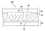
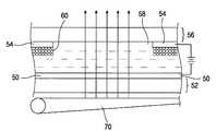
도 5는 본 발명에 따른 EPD 셀(200)의 단면을 도시한 단면도이다.5 is a cross-sectional view showing a cross section of the
상기 EPD 셀(200)의 구성을 살펴보면, 제 1 기판(1a)과 상기 제 1 기판(1a)의 전면에 형성된 제 1 전극(50)을 포함하는 하판(52)과, 제 2 기판(1b)과 상기 제 2 기판(1b)의 가장자리에 형성된 제 2 전극(54)을 포함하는 상판(56)으로 구성되며, 상기 상판(56)과 하판(52) 사이에는 전기영동을 하는 염료입자(dye particle ; 60)가 소정의 액체(58)와 혼합된 형태로 구성된다.Looking at the configuration of the
상기 전기영동(electrophoresis ; EP)현상이란 소정의 용기내에 물 또는 기타 액체를 넣고, 이 속에 상기 액체와 섞이지 않는 다른 액 또는 고체입자 등을 부유(suspension)시킨다. 그리고, 상기 고체입자 등이 부유하는 액체속에 전극을 삽입하고, 직류전압을 인가하면 상기 액체속에 부유하는 고체입자는 대전됨과 동시에 어느 한 전극으로 모이게 되는 현상을 전기영동(電氣泳動)이라 한다.The electrophoresis (EP) phenomenon is to put water or other liquid into a predetermined container, and to suspend other liquid or solid particles, etc. which are not mixed with the liquid therein. When the electrode is inserted into a liquid in which the solid particles and the like are suspended, and a direct current voltage is applied, the phenomenon in which the solid particles in the liquid are charged and collected at one electrode is called electrophoresis.
상기 고체입자의 성질에 따라서 대전되는 극성이 다르게 되며, 따라서 영동하는 물질도 음극을 향하는 것과 양극을 향하는 것이 있으며, 각각 캐타페리시스(cataphoresis) 및 애나페리시스(anaphoresis)라 한다.Depending on the properties of the solid particles, the charged polarity is different, and thus, the electrophoretic material may face the cathode and the anode, respectively, and are referred to as cataphoresis and anaphoresis, respectively.
본 발명에서는 상술한 전기영동 현상을 이용하여 반사와 투과가 가능한 EPD 셀을 구성하는 것이다.In the present invention, the electrophoretic phenomenon described above constitutes an EPD cell capable of reflection and transmission.
여기서, 상기 액체(58)는 투명한 솔벤트(solvent)가 사용되며, 기타 다른 용액이 사용될 수 있다. 그리고, 상기 제 1 전극(50)은 바람직하게는 투명전극(transparent conducting oxide ; TCO)을 사용하며, 그 종류로는 인듐-틴 옥사이드(ITO)가 사용된다.In this case, the liquid 58 may be used as a transparent solvent, and other solutions may be used. In addition, the
또한, 상기 제 2 전극(54)은 집진전극(collecting electrode)이라고도 한다. 이는 도 6a에서 자세히 설명될 것이다.The
도 6a 내지 도 6b는 본 발명의 실시예에 따른 EPD 셀의 동작을 나타내는 단면도이다.6A through 6B are cross-sectional views illustrating the operation of an EPD cell according to an embodiment of the present invention.
즉, 상기 도 6a는 상기 제 1 및 제 2 전극(50, 54)에 각각 음 및 양의 직류전압을 인가 했을 경우 염료입자(60)의 전기영동을 도시한 것이다. 여기서 상기 염료입자(60)은 양의 전하로 대전 되었다고 가정한다.That is, FIG. 6A illustrates electrophoresis of the
이 때, 양의 전하로 대전된 염료입자(60)는 음의 전압이 인가된 제 2 전극(54)으로 모이게 된다. 따라서, 상기 제 2 전극(54)은 상기 염료입자(60)를 모으기 때문에 집전전극의 역할을 하게 된다.At this time, the
따라서, 상기 EPD 셀의 하부에 백라이트(70)를 설치하면 상기 백라이트(70)에서 방출된 빛은 상기 염료입자의 저항없이 하판(52)과 액체(58) 및 상판(56)을 투과할 수 있다. 즉, 상기 염료입자(60)를 집전하는 제 2 전극에 상기 염료입자(60)가 모여서 결과적으로는 백라이트 광이 투과할 수 있는 상태가 되는 것이다.Therefore, when the
도 6b는 상기 제 1 및 제 2 전극(50, 54)에 각각 양 및 음의 직류 전압을 인가 했을 경우의 염료입자(60)의 전기 영동을 도시한 도면이다. 즉, 도 6a 와 비교해서 상기 양의 전하로 대전된 염료입자(60)는 상기 제 1 전극(50)으로 모여서 상기 제 1 전극(50)의 표면에 정렬되는 것을 알 수 있다.6B is a diagram illustrating electrophoresis of the
즉, 상기 제 1 전극(50) 표면에 정렬된 염료입자(60)는 외부에서 입사된 광을 다시 외부로 반사시키는 반사판의 역할을 하게 된다.That is, the
상술한 EPD 셀은 메모리 효과(memory effect)가 있다. 즉, 상기 EPD 셀에 인가한 직류전압을 제거해도 도 6a 또는 도 6b에서와 같이, 제 2 또는 제 1 전극에 모인 상기 염료입자(60)는 그 상태를 계속 유지하게 된다. 따라서, 한번 전기장을 인가하고 바로 제거하여도 전기영동 상태가 유지되기 때문에 추가적인 전력소비 없이 반사 또는 투과 모드를 유지할 수 있다.The aforementioned EPD cell has a memory effect. That is, even if the DC voltage applied to the EPD cell is removed, as shown in FIG. 6A or 6B, the
상술한 EPD 셀의 구성은 염료입자의 집전을 위한 제 2 전극을 상판에 설치하였으나, 상기 제 2 전극을 하판에 설치하여 상기 EPD 셀을 반사모드로 사용할 때, 염료입자의 반사판 형성을 상판에 형성할 수도 있을 것이다.In the above-described configuration of the EPD cell, the second electrode for collecting current of the dye particles is provided on the upper plate, but when the second electrode is installed on the lower plate and the EPD cell is used in the reflection mode, the formation of the reflector plate of the dye particles is formed on the upper plate. You could do it.
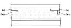
또한, 도 7에 도시된 바와 같이 상기 집전전극인 제 2 전극을 EPD 셀의 측면에도 설치하면, 전기영동입자(염료입자)의 포집을 더욱 강화할 수 있을 것이다.In addition, as shown in FIG. 7, if the second electrode, which is the current collecting electrode, is also provided on the side of the EPD cell, the collection of electrophoretic particles (dye particles) may be further enhanced.
즉, 집전전극(제 2 전극; 54, 54a)의 표면적을 증가시킴으로써, 전기장의 세기를 증가시켜 상기 EPD 셀의 염료입자의 포집력을 강화하는 것이다.That is, by increasing the surface area of the current collecting electrodes (second electrode) 54, 54a, the intensity of the electric field is increased to enhance the collecting power of the dye particles of the EPD cell.
도 8은 본 발명에 따른 EPD 셀을 실제적으로 반사/투과형 액정 표시장치에 적용한 구조의 단면을 개략적으로 도시한 단면도이다.8 is a cross-sectional view schematically illustrating a cross section of a structure in which an EPD cell according to the present invention is actually applied to a reflective / transmissive liquid crystal display device.
도 8의 반사/투과형 액정 표시장치의 구성은 크게 세 부분으로 구분할 수 있으며, 그 구성은 실제적으로 광의 변조가 일어나는 액정 셀과 광 셔터의 작용을 하는 EPD 셀과 인조광을 발생하는 백라이트로 구분될 수 있다.The configuration of the reflective / transmissive liquid crystal display of FIG. 8 can be largely divided into three parts. The configuration of the reflective / transmissive liquid crystal display of FIG. 8 can be divided into a liquid crystal cell in which light modulation is actually performed, an EPD cell acting as an optical shutter, and a backlight for generating artificial light. Can be.
상기 액정 셀은 스위칭 소자인 다수의 박막 트랜지스터(미도시)와 상기 각 박막 트랜지스터와 일대일 대응하는 화소전극(400)이 형성된 박막 트랜지스터 기판(402)과, 컬러필터층(404)과 상기 컬러필터층(404)을 덮는 형태로 형성된 공통전극(406)을 포함하는 컬러필터 기판(408)과, 상기 박막 트랜지스터 기판(402)과 상기 컬러필터 기판(408) 사이에 형성된 액정층(410)으로 구성된다.The liquid crystal cell includes a thin
그리고, 상기 EPD 셀은 상기 박막 트랜지스터 기판(402) 하부에 위치하며, 그 구성에 관해서는 이미 상술했기 때문에 그 설명을 생략한다.In addition, since the EPD cell is located under the thin
또한, 상기 EPD 셀 하부에는 백라이트가 위치한다.In addition, a backlight is located under the EPD cell.
상술한 바와 같이, 본 발명에 따른 EPD 셀을 채용한 반사/투과형 액정 표시장치의 동작을 살펴보면 다음과 같다.As described above, the operation of the reflective / transmissive liquid crystal display device employing the EPD cell according to the present invention is as follows.
먼저, 반사형 모드에서 동작을 살펴보면, 염료입자(60)가 양의 전하로 대전되었다고 가정할 때, 상기 EPD 셀의 제 1 전극에 음의 전압을 인가하고, 제 2 전극(집전전극 ; 54)에 양의 전압을 인가하면, 상기 양의 전하로 대전된 염료입자(60)는 상기 제 1 전극(50)의 표면 전체에 정렬할 것이고, 상기 정렬된 염료입자는 반사판의 역할을 하게되어 외부 광을 반사시키는 기능을 수행하게 된다.First, referring to the operation in the reflective mode, assuming that the
그리고, 투과모드에서는 상기 EPD 셀의 제 1 전극에 양의 전압을 인가하고 제 2 전극(집전전극 ; 54)에 음의 전압을 인가하면, 양의 전하로 대전된 염료입자(60)는 상기 제 2 전극(54)인 집전전극에 분리되어 모이게 된다. 따라서 백라이트로부터 방출되는 백라이트 광이 상기 액정 셀을 통해 외부로 방출되기에 충분한 상태가 되는 것이다.In the transmissive mode, when a positive voltage is applied to the first electrode of the EPD cell and a negative voltage is applied to the second electrode (current collecting electrode) 54, the
상술한 바와 같이 본 발명의 바람직한 실시예를 따라 EPD 셀을 채용한 반사투과형 TFT-LCD를 제작할 경우에 기존의 반사/투과형 액정 표시장치에 비해 광 이용 효율이 증대되어, 향상된 화질을 얻을 수 있다.As described above, when the reflective TFT-LCD employing the EPD cell is manufactured according to the preferred embodiment of the present invention, the light utilization efficiency is increased as compared with the conventional reflective / transmissive liquid crystal display device, thereby obtaining improved image quality.
또한, 상기 EPD 셀의 집전전극을 셀의 측면에도 설치하여 대전입자의 포집력을 향상할 수 있을 것이다.In addition, the collecting electrode of the EPD cell may be installed on the side of the cell to improve the collecting force of the charged particles.
또한, 상기 EDP 셀에서 집전전극과 투명전극의 위치를 바꾸어 EDP 셀을 형성하면, 반사모드시에 외부광이 용매를 투과하지 않고 바로 대전입자에 반사되므로 반사효율이 더욱더 극대화될 수 있는 장점이 있다.In addition, when the EDP cell is formed by changing the positions of the current collecting electrode and the transparent electrode in the EDP cell, the external light does not penetrate the solvent in the reflective mode and is immediately reflected by the charged particles, which has the advantage that the reflection efficiency can be further maximized. .
Claims (9)
Translated fromKoreanPriority Applications (2)
| Application Number | Priority Date | Filing Date | Title |
|---|---|---|---|
| KR1019990041434AKR100575452B1 (en) | 1999-09-28 | 1999-09-28 | Reflective type liquid crystal display using electrophoretic display and electrophoretic display |
| US09/670,836US6621541B1 (en) | 1999-09-28 | 2000-09-28 | Transflective liquid crystal display device having an electrophoretic display |
Applications Claiming Priority (1)
| Application Number | Priority Date | Filing Date | Title |
|---|---|---|---|
| KR1019990041434AKR100575452B1 (en) | 1999-09-28 | 1999-09-28 | Reflective type liquid crystal display using electrophoretic display and electrophoretic display |
Publications (2)
| Publication Number | Publication Date |
|---|---|
| KR20010028910A KR20010028910A (en) | 2001-04-06 |
| KR100575452B1true KR100575452B1 (en) | 2006-05-03 |
Family
ID=19612979
Family Applications (1)
| Application Number | Title | Priority Date | Filing Date |
|---|---|---|---|
| KR1019990041434AExpired - Fee RelatedKR100575452B1 (en) | 1999-09-28 | 1999-09-28 | Reflective type liquid crystal display using electrophoretic display and electrophoretic display |
Country Status (2)
| Country | Link |
|---|---|
| US (1) | US6621541B1 (en) |
| KR (1) | KR100575452B1 (en) |
Families Citing this family (48)
| Publication number | Priority date | Publication date | Assignee | Title |
|---|---|---|---|---|
| WO2003019279A1 (en)* | 2001-08-23 | 2003-03-06 | Koninklijke Philips Electronics N.V. | Electrophoretic display device |
| KR100426963B1 (en)* | 2001-10-12 | 2004-04-14 | 엘지.필립스 엘시디 주식회사 | transflective liquid crystal display devices |
| JP3956287B2 (en)* | 2002-04-26 | 2007-08-08 | 株式会社 日立ディスプレイズ | Liquid crystal display |
| TW567377B (en)* | 2002-06-13 | 2003-12-21 | Toppoly Optoelectronics Corp | Transmission-reflection switch liquid crystal display |
| JP4427942B2 (en)* | 2002-08-29 | 2010-03-10 | 富士ゼロックス株式会社 | Image writing device |
| TW200428082A (en)* | 2002-11-15 | 2004-12-16 | Matsushita Electric Industrial Co Ltd | Display device and method for driving same |
| JP2004233838A (en)* | 2003-01-31 | 2004-08-19 | Canon Inc | Electrophoretic display element and method of manufacturing the same |
| US20050012707A1 (en)* | 2003-07-15 | 2005-01-20 | Hong-Da Liu | Electrophoretic display and a method of driving said display |
| US20050012708A1 (en)* | 2003-07-15 | 2005-01-20 | Hong-Da Liu | Electrophoretic display and a method of driving said display |
| JP4076222B2 (en)* | 2003-07-25 | 2008-04-16 | 株式会社東芝 | Electrophoretic display device |
| GB0322231D0 (en)* | 2003-09-23 | 2003-10-22 | Koninkl Philips Electronics Nv | Transflector and transflective display |
| JP4386037B2 (en)* | 2003-09-30 | 2009-12-16 | セイコーエプソン株式会社 | Image display device |
| KR100957613B1 (en)* | 2003-12-23 | 2010-05-13 | 엘지디스플레이 주식회사 | Electrophoretic display driving method |
| KR101035162B1 (en)* | 2004-10-29 | 2011-05-17 | 엘지디스플레이 주식회사 | Upper case and digital paper display device using the same |
| US7417785B2 (en)* | 2005-01-18 | 2008-08-26 | Research Frontiers Incorporated | Methods and circuits for distributing power to SPD loads |
| GB0504265D0 (en)* | 2005-03-02 | 2005-04-06 | Eastman Kodak Co | Method of making an address plate |
| TWI306533B (en)* | 2005-03-15 | 2009-02-21 | Ind Tech Res Inst | A transflective electrophoresis display and manufacturing method |
| TWI446004B (en)* | 2005-06-14 | 2014-07-21 | Koninkl Philips Electronics Nv | Combined single/multiple view-display |
| CN100465749C (en)* | 2005-07-18 | 2009-03-04 | 财团法人工业技术研究院 | Electrophoretic display with transflective transparent film and manufacturing method thereof |
| GB0611125D0 (en)* | 2006-06-06 | 2006-07-19 | Liquavista Bv | Transflective electrowetting display device |
| KR100967259B1 (en)* | 2006-08-29 | 2010-07-01 | 엘지디스플레이 주식회사 | Display device of a mobile terminal |
| KR101298173B1 (en)* | 2006-12-05 | 2013-08-20 | 삼성디스플레이 주식회사 | Color filter substrate and electro-phoretic display device having the same |
| KR101329139B1 (en)* | 2007-10-12 | 2013-11-14 | 삼성전자주식회사 | System and method for controling switching display performing transmitive mode /trasflective mode/ reflective mode |
| EP2245506A4 (en)* | 2008-02-26 | 2011-05-11 | Hewlett Packard Development Co | ELECTROPHORETIC DISPLAY DEVICE |
| WO2009106132A1 (en)* | 2008-02-26 | 2009-09-03 | Hewlett-Packard Development Company, L.P. | Passive electrophoretic liquid crystal display device |
| KR101159623B1 (en)* | 2008-03-11 | 2012-06-27 | 삼성전자주식회사 | Display device displaying still image consuming small amount of electric power and method for displaying still image using the same |
| KR20100004031A (en) | 2008-07-02 | 2010-01-12 | 삼성전자주식회사 | Transparent display device and manufacturing method thereof |
| US8330882B2 (en)* | 2009-02-25 | 2012-12-11 | Industrial Technology Research Institute | Image display capable of being an electronic curtain |
| US8284118B2 (en)* | 2009-04-03 | 2012-10-09 | Verizon Patent And Licensing Inc. | Power saving mode in persistently active multi-layer display screen |
| EP2452332B1 (en)* | 2009-07-07 | 2019-01-02 | Dolby Laboratories Licensing Corporation | Edge-lit local dimming displays, display components and related methods |
| US9201282B2 (en)* | 2009-07-27 | 2015-12-01 | Hj Forever Patents B.V. | Electrophoretic display device |
| US8648772B2 (en)* | 2009-08-20 | 2014-02-11 | Amazon Technologies, Inc. | Amalgamated display comprising dissimilar display devices |
| EP2513716A1 (en)* | 2009-12-18 | 2012-10-24 | Hewlett Packard Development Company, L.P. | Reflective display |
| TW201133437A (en)* | 2010-03-23 | 2011-10-01 | Wistron Corp | Method of switching screen and electronic apparatus used to implement the method |
| US20110292319A1 (en)* | 2010-05-27 | 2011-12-01 | E Ink Corporation | Dual mode electro-optic displays |
| JP5423603B2 (en)* | 2010-07-26 | 2014-02-19 | 日立化成株式会社 | Suspended particle device and driving method thereof |
| TWM396973U (en) | 2010-07-29 | 2011-01-21 | Chunghwa Picture Tubes Ltd | Transflective display device |
| KR20120127085A (en)* | 2011-05-13 | 2012-11-21 | 삼성디스플레이 주식회사 | Display device |
| US20120320308A1 (en)* | 2011-06-20 | 2012-12-20 | Jong-Souk Yeo | Transflective displays |
| TW201303461A (en)* | 2011-07-04 | 2013-01-16 | Chunghwa Picture Tubes Ltd | Display device |
| TWI467308B (en)* | 2012-03-16 | 2015-01-01 | E Ink Holdings Inc | Electrophoretic display apparatus |
| CN103969874B (en)* | 2014-04-28 | 2017-02-15 | 京东方科技集团股份有限公司 | Liquid crystal display panel, manufacturing method, semitransparent and semi-reflecting display device and display control method |
| NL2012803B1 (en) | 2014-05-12 | 2016-02-24 | Hj Forever Patents B V | Electrophoretic display. |
| DE102016111159A1 (en)* | 2016-06-17 | 2017-12-21 | Visteon Global Technologies, Inc. | Display arrangement and method for displaying information |
| CN106483694B (en)* | 2017-01-03 | 2019-09-27 | 京东方科技集团股份有限公司 | Display screen, display device and display method |
| JP2021060447A (en)* | 2019-10-03 | 2021-04-15 | 株式会社ジャパンディスプレイ | Display device and driving method for display device |
| CN111708216B (en)* | 2020-07-14 | 2023-12-29 | 京东方科技集团股份有限公司 | Display device and electronic equipment |
| CN112068379B (en)* | 2020-09-10 | 2023-01-10 | 深圳市华星光电半导体显示技术有限公司 | Reflection-transmission switchable device, preparation method thereof and display device |
Citations (6)
| Publication number | Priority date | Publication date | Assignee | Title |
|---|---|---|---|---|
| JPS59171930A (en)* | 1983-03-18 | 1984-09-28 | Matsushita Electric Ind Co Ltd | Electrophoresis display element |
| JPS59171931A (en)* | 1983-03-18 | 1984-09-28 | Matsushita Electric Ind Co Ltd | electrophoretic display element |
| JPH05173193A (en)* | 1991-12-25 | 1993-07-13 | Dainippon Printing Co Ltd | Dispersed system for electrophoretic display and electrophoretic display element using the dispersed system |
| JPH06110088A (en)* | 1992-09-25 | 1994-04-22 | Nippon Mektron Ltd | Driving system of electrophoretic display device |
| JPH09211499A (en)* | 1996-01-30 | 1997-08-15 | Toshiba Corp | Electrophoretic display |
| JPH10161161A (en)* | 1996-12-04 | 1998-06-19 | Fuji Xerox Co Ltd | Sheet like display medium and display device |
Family Cites Families (2)
| Publication number | Priority date | Publication date | Assignee | Title |
|---|---|---|---|---|
| US5587264A (en)* | 1989-03-16 | 1996-12-24 | Dai Nippon Printing Co. Ltd. | Electrostatic information recording medium and electrostatic information recording and reproducing method |
| US5493430A (en)* | 1994-08-03 | 1996-02-20 | Kent Display Systems, L.P. | Color, reflective liquid crystal displays |
- 1999
- 1999-09-28KRKR1019990041434Apatent/KR100575452B1/ennot_activeExpired - Fee Related
- 2000
- 2000-09-28USUS09/670,836patent/US6621541B1/ennot_activeExpired - Lifetime
Patent Citations (6)
| Publication number | Priority date | Publication date | Assignee | Title |
|---|---|---|---|---|
| JPS59171930A (en)* | 1983-03-18 | 1984-09-28 | Matsushita Electric Ind Co Ltd | Electrophoresis display element |
| JPS59171931A (en)* | 1983-03-18 | 1984-09-28 | Matsushita Electric Ind Co Ltd | electrophoretic display element |
| JPH05173193A (en)* | 1991-12-25 | 1993-07-13 | Dainippon Printing Co Ltd | Dispersed system for electrophoretic display and electrophoretic display element using the dispersed system |
| JPH06110088A (en)* | 1992-09-25 | 1994-04-22 | Nippon Mektron Ltd | Driving system of electrophoretic display device |
| JPH09211499A (en)* | 1996-01-30 | 1997-08-15 | Toshiba Corp | Electrophoretic display |
| JPH10161161A (en)* | 1996-12-04 | 1998-06-19 | Fuji Xerox Co Ltd | Sheet like display medium and display device |
Also Published As
| Publication number | Publication date |
|---|---|
| US6621541B1 (en) | 2003-09-16 |
| KR20010028910A (en) | 2001-04-06 |
Similar Documents
| Publication | Publication Date | Title |
|---|---|---|
| KR100575452B1 (en) | Reflective type liquid crystal display using electrophoretic display and electrophoretic display | |
| US5745094A (en) | Electrophoretic display | |
| KR100641628B1 (en) | Reflective and Transflective Liquid Crystal Display Using Black Resin | |
| KR100688230B1 (en) | Transflective liquid crystal display device | |
| KR100312328B1 (en) | Transflective liquid crystal display device | |
| JPS60165621A (en) | Transmission type display element | |
| JPH0756547B2 (en) | Transmissive display element | |
| JP2000019563A5 (en) | ||
| US7589800B2 (en) | Method of driving liquid crystal display device | |
| JPS60165622A (en) | Transmission type display element | |
| JPS60165624A (en) | Transmission type display element | |
| KR100613438B1 (en) | Reflective type liquid crystal display device and manufacturing method thereof | |
| CN100403107C (en) | Liquid crystal display device with a light guide plate | |
| US20070070274A1 (en) | Transflective liquid crystal display having electrically connected reflective electrodes | |
| CN111198493B (en) | Display device and intelligent watch | |
| CN115718385B (en) | Reflective display panel and display device | |
| KR100613437B1 (en) | Reflective transmission liquid crystal display | |
| JP2003195362A (en) | Electrophoretic display and electronic equipment | |
| CN116165818A (en) | Display panel, control method thereof, and display device | |
| US6999106B2 (en) | Reducing the bias on silicon light modulators | |
| KR20050110392A (en) | Electrophoretic display device | |
| KR20010015373A (en) | Reflection and transmission type liquid crystal display device | |
| Fleming et al. | 36‐3: Tablet‐size eTIR Display for Low‐power ePaper Applications with Color Video Capability | |
| CN222232841U (en) | Color electronic paper display device | |
| CN222232830U (en) | Display panel and display device |
Legal Events
| Date | Code | Title | Description |
|---|---|---|---|
| PA0109 | Patent application | St.27 status event code:A-0-1-A10-A12-nap-PA0109 | |
| PG1501 | Laying open of application | St.27 status event code:A-1-1-Q10-Q12-nap-PG1501 | |
| PN2301 | Change of applicant | St.27 status event code:A-3-3-R10-R13-asn-PN2301 St.27 status event code:A-3-3-R10-R11-asn-PN2301 | |
| A201 | Request for examination | ||
| PA0201 | Request for examination | St.27 status event code:A-1-2-D10-D11-exm-PA0201 | |
| R17-X000 | Change to representative recorded | St.27 status event code:A-3-3-R10-R17-oth-X000 | |
| D13-X000 | Search requested | St.27 status event code:A-1-2-D10-D13-srh-X000 | |
| D14-X000 | Search report completed | St.27 status event code:A-1-2-D10-D14-srh-X000 | |
| E701 | Decision to grant or registration of patent right | ||
| PE0701 | Decision of registration | St.27 status event code:A-1-2-D10-D22-exm-PE0701 | |
| GRNT | Written decision to grant | ||
| PR0701 | Registration of establishment | St.27 status event code:A-2-4-F10-F11-exm-PR0701 | |
| PR1002 | Payment of registration fee | St.27 status event code:A-2-2-U10-U11-oth-PR1002 Fee payment year number:1 | |
| PG1601 | Publication of registration | St.27 status event code:A-4-4-Q10-Q13-nap-PG1601 | |
| PN2301 | Change of applicant | St.27 status event code:A-5-5-R10-R13-asn-PN2301 St.27 status event code:A-5-5-R10-R11-asn-PN2301 | |
| PR1001 | Payment of annual fee | St.27 status event code:A-4-4-U10-U11-oth-PR1001 Fee payment year number:4 | |
| PR1001 | Payment of annual fee | St.27 status event code:A-4-4-U10-U11-oth-PR1001 Fee payment year number:5 | |
| R18-X000 | Changes to party contact information recorded | St.27 status event code:A-5-5-R10-R18-oth-X000 | |
| PR1001 | Payment of annual fee | St.27 status event code:A-4-4-U10-U11-oth-PR1001 Fee payment year number:6 | |
| R18-X000 | Changes to party contact information recorded | St.27 status event code:A-5-5-R10-R18-oth-X000 | |
| R18-X000 | Changes to party contact information recorded | St.27 status event code:A-5-5-R10-R18-oth-X000 | |
| FPAY | Annual fee payment | Payment date:20120330 Year of fee payment:7 | |
| PR1001 | Payment of annual fee | St.27 status event code:A-4-4-U10-U11-oth-PR1001 Fee payment year number:7 | |
| FPAY | Annual fee payment | Payment date:20130329 Year of fee payment:8 | |
| PR1001 | Payment of annual fee | St.27 status event code:A-4-4-U10-U11-oth-PR1001 Fee payment year number:8 | |
| PR1001 | Payment of annual fee | St.27 status event code:A-4-4-U10-U11-oth-PR1001 Fee payment year number:9 | |
| PR1001 | Payment of annual fee | St.27 status event code:A-4-4-U10-U11-oth-PR1001 Fee payment year number:10 | |
| FPAY | Annual fee payment | Payment date:20160329 Year of fee payment:11 | |
| PR1001 | Payment of annual fee | St.27 status event code:A-4-4-U10-U11-oth-PR1001 Fee payment year number:11 | |
| FPAY | Annual fee payment | Payment date:20170320 Year of fee payment:12 | |
| PR1001 | Payment of annual fee | St.27 status event code:A-4-4-U10-U11-oth-PR1001 Fee payment year number:12 | |
| PR1001 | Payment of annual fee | St.27 status event code:A-4-4-U10-U11-oth-PR1001 Fee payment year number:13 | |
| LAPS | Lapse due to unpaid annual fee | ||
| PC1903 | Unpaid annual fee | St.27 status event code:A-4-4-U10-U13-oth-PC1903 Not in force date:20190426 Payment event data comment text:Termination Category : DEFAULT_OF_REGISTRATION_FEE | |
| P22-X000 | Classification modified | St.27 status event code:A-4-4-P10-P22-nap-X000 | |
| PC1903 | Unpaid annual fee | St.27 status event code:N-4-6-H10-H13-oth-PC1903 Ip right cessation event data comment text:Termination Category : DEFAULT_OF_REGISTRATION_FEE Not in force date:20190426 |