KR100575351B1 - Infrared receiver with noise canceling function - Google Patents
Infrared receiver with noise canceling functionDownload PDFInfo
- Publication number
- KR100575351B1 KR100575351B1KR1020030001130AKR20030001130AKR100575351B1KR 100575351 B1KR100575351 B1KR 100575351B1KR 1020030001130 AKR1020030001130 AKR 1020030001130AKR 20030001130 AKR20030001130 AKR 20030001130AKR 100575351 B1KR100575351 B1KR 100575351B1
- Authority
- KR
- South Korea
- Prior art keywords
- signal
- unit
- output
- infrared ray
- output signal
- Prior art date
- Legal status (The legal status is an assumption and is not a legal conclusion. Google has not performed a legal analysis and makes no representation as to the accuracy of the status listed.)
- Expired - Lifetime
Links
- 239000003990capacitorSubstances0.000claimsabstractdescription21
- 238000001914filtrationMethods0.000claimsabstractdescription3
- 238000007599dischargingMethods0.000claimsdescription6
- 230000005059dormancyEffects0.000claims2
- 238000005516engineering processMethods0.000abstractdescription2
- 238000010586diagramMethods0.000description9
- 230000008878couplingEffects0.000description5
- 238000010168coupling processMethods0.000description5
- 238000005859coupling reactionMethods0.000description5
- 238000001514detection methodMethods0.000description4
- 238000000034methodMethods0.000description4
- 230000003321amplificationEffects0.000description3
- 230000008859changeEffects0.000description3
- 230000001276controlling effectEffects0.000description3
- 238000003199nucleic acid amplification methodMethods0.000description3
- 238000007796conventional methodMethods0.000description2
- 230000007423decreaseEffects0.000description2
- 230000007257malfunctionEffects0.000description2
- 238000012545processingMethods0.000description2
- 230000002159abnormal effectEffects0.000description1
- 230000002238attenuated effectEffects0.000description1
- 238000013461designMethods0.000description1
- 238000011161developmentMethods0.000description1
- 230000000694effectsEffects0.000description1
- 230000003993interactionEffects0.000description1
- 238000012986modificationMethods0.000description1
- 230000004048modificationEffects0.000description1
- 230000003287optical effectEffects0.000description1
- 230000008569processEffects0.000description1
- 230000009467reductionEffects0.000description1
- 230000001105regulatory effectEffects0.000description1
- 230000000284resting effectEffects0.000description1
Images


Classifications
- H—ELECTRICITY
- H04—ELECTRIC COMMUNICATION TECHNIQUE
- H04B—TRANSMISSION
- H04B10/00—Transmission systems employing electromagnetic waves other than radio-waves, e.g. infrared, visible or ultraviolet light, or employing corpuscular radiation, e.g. quantum communication
- H04B10/60—Receivers
- H04B10/66—Non-coherent receivers, e.g. using direct detection
- H04B10/69—Electrical arrangements in the receiver
- H04B10/693—Arrangements for optimizing the preamplifier in the receiver
- H04B10/6931—Automatic gain control of the preamplifier
- H—ELECTRICITY
- H04—ELECTRIC COMMUNICATION TECHNIQUE
- H04B—TRANSMISSION
- H04B1/00—Details of transmission systems, not covered by a single one of groups H04B3/00 - H04B13/00; Details of transmission systems not characterised by the medium used for transmission
- H04B1/06—Receivers
- H04B1/10—Means associated with receiver for limiting or suppressing noise or interference
- H04B1/1027—Means associated with receiver for limiting or suppressing noise or interference assessing signal quality or detecting noise/interference for the received signal
- H—ELECTRICITY
- H04—ELECTRIC COMMUNICATION TECHNIQUE
- H04B—TRANSMISSION
- H04B10/00—Transmission systems employing electromagnetic waves other than radio-waves, e.g. infrared, visible or ultraviolet light, or employing corpuscular radiation, e.g. quantum communication
- H04B10/60—Receivers
- H04B10/66—Non-coherent receivers, e.g. using direct detection
- H04B10/69—Electrical arrangements in the receiver
- H04B10/697—Arrangements for reducing noise and distortion
- H04B10/6972—Arrangements for reducing noise and distortion using passive filtering
Landscapes
- Engineering & Computer Science (AREA)
- Computer Networks & Wireless Communication (AREA)
- Signal Processing (AREA)
- Physics & Mathematics (AREA)
- Electromagnetism (AREA)
- Optical Communication System (AREA)
- Selective Calling Equipment (AREA)
Abstract
Translated fromKoreanDescription
Translated fromKorean도 1은 종래의 적외선 수신장치의 블럭도를 도시한 것이다.1 is a block diagram of a conventional infrared ray receiving apparatus.
도 2는 본 발명에 의한 노이즈 제거 기능을 갖는 적외선 수신장치의 블럭도를 도시한 것이다.2 is a block diagram of an infrared ray receiving apparatus having a noise removing function according to the present invention.
도 3은 본 발명에 의한 노이즈 제거 기능을 갖는 적외선 수신장치 중 자동이득조절부, 비교부, 복조부 및 출력회로부를 나타내는 상세 회로도를 도시한 것이다.3 is a detailed circuit diagram showing an automatic gain control unit, a comparison unit, a demodulation unit, and an output circuit unit of an infrared ray receiving apparatus having a noise removing function according to the present invention.
도 4는 본 발명에 의한 노이즈 제거 기능을 갖는 적외선 수신장치의 동작을 나타내는 플로우 차트를 도시한 것이다.4 is a flowchart showing an operation of an infrared ray receiving apparatus having a noise removing function according to the present invention.
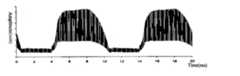
도 5는 적외선 수신장치에 입력되는 정상 신호와 복조가 완성된 신호의 실시 예를 도시한 것이다.FIG. 5 shows an example of a normal signal inputted to the infrared ray receiving apparatus and a signal demodulated.
도 6은 강변조되어 적외선 수신장치내부로 유입된 형광램프 노이즈 신호의 실시예를 도시한 것이다.FIG. 6 shows an embodiment of a fluorescent lamp noise signal which is transformed into a river and introduced into the infrared ray receiving apparatus.
도 7은 약변조되어 적외선 수신장치내부로 유입된 형광램프 노이즈 신호의 실시예를 도시한 것이다.FIG. 7 shows an embodiment of a fluorescent lamp noise signal modulated and input into the infrared ray receiving apparatus.
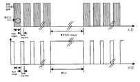
도 8은 AGC 인터페이스부의 간략 회로도를 도시한 것이다.8 shows a simplified circuit diagram of the AGC interface unit.
도 9는 도 8의 타이밍 도를 도시한 것이다.Fig. 9 shows the timing chart of Fig.
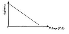
도 10은 자동이득조절증폭기의 이득과 조절전압과의 관계 그래프를 도시한 것이다.10 is a graph showing a relationship between the gain of the automatic gain control amplifier and the regulated voltage.
<도면의 주요부분에 대한 부호의 설명>Description of the Related Art
10 : 포토 다이오드11 : 제1 증폭부(AV1)10: photodiode 11: first amplifier (AV1)
12 : 제2증폭부(AV2) 혹은 자동이득조절증폭기(AGC amp)12: a second amplifying unit (AV2) or an automatic gain control amplifier (AGC amp)
13 : 대역통과필터(BPF)14 : 비교부(comparator block)13: band pass filter (BPF) 14: comparator block
15 : 복조부(demodulator block)16 : 슈미트 회로부15: demodulator block 16: schmitt circuit
17 : 자동이득조절부(AGC)TR11 :최종출력 트랜지스터17: Automatic gain control section (AGC) TR11: Final output transistor
R11 : 풀업(pull up) 저항R11: pull up resistance
본원 발명은 TV나 VCR등의 가전제품에 사용되는 적외선 리모콘이나 기타 적외선 데이터 송신 장치로부터 적외선 신호를 받아서 처리하는 적외선 수신장치에 관한 것으로, 좀 더 상세하게는 적외선 수신장치에 입력되는 신호의 특성에 따라 입력신호가 노이즈인지 정상적인 신호인지 판단하는 기술에 관한 것이다.BACKGROUND OF THE INVENTION 1. Field of the Invention The present invention relates to an infrared ray receiving apparatus for receiving and processing an infrared ray signal from an infrared remote controller or other infrared data transmitting apparatus used in household appliances such as TVs and VCRs, To a technique for judging whether an input signal is a noise or a normal signal.
도1은 종래의 적외선 수신장치를 블록도 형식으로 나타낸 것이다. 도1의 그림이 모든 종류의 적외선 수신장치를 완벽히 표시하고 있지는 않으나 대개는 도 1 과 같은 형태를 띄고 있다. 종래의 적외선 수신장치의 동작을 도1을 참조하여 설명하면 다음과 같다.1 is a block diagram of a conventional infrared ray receiving apparatus. Although FIG. 1 does not completely show all types of infrared ray receiving apparatuses, the infrared ray receiving apparatuses are generally shown in FIG. 1. The operation of the conventional infrared ray receiving apparatus will be described with reference to FIG.
우선 포토 다이오드(10)가 외부로부터의 적외선 신호를 감지하여 적외선 신호를 전기 신호로 바꾸어 주고, 이러한 전기신호는 미약한 신호이므로 제1증폭기 AV1 (11)를 통하여 적절한 값으로 증폭한다. 제1증폭기(11)로부터 출력된 신호는 제1 커플링 커패시터(C11)를 통하여 제2 증폭기(12), 즉 리미터 증폭기 AV2에 전달된다. 리미터 증폭기(12)에 의해 또 다시 증폭된 신호는 다시 제2 커플링 커패시터(C12)를 거치게 된다. 제1 및 제2 커패시터의 역할은 각 증폭기의 출력이 포함하고 있거나 포함하고 있을지도 모를 직류(DC)신호성분을 적절하게 걸러주기 위한 것이다. 제2 커플링 커패시터를 통과한 신호는 대역통과필터(Band Pass Filter:BPF)(13)를 거쳐서 적절한 주파수 대역폭을 가진 신호만이 걸러진다. 대역통과필터의 출력신호는 다시 비교부(14)의 입력으로 연결된다.
비교부(14)의 또 다른 입력은 비교기 기준전압에 연결되어 있고 비교부(14)는 비교기 기준전압과 대역통과필터의 출력신호의 전압을 비교하는 동작을 한다. 비교부(14)의 출력은 복조부(15)와 연결되어 있고, 복조부의 출력신호는 슈미트 트리거(16)를 통하여 출력회로부로 전달된다. 출력회로부는 출력트랜지스터(TR11)와 풀-업(pull-up) 저항(R11)으로 구성되고 대개의 출력트랜지스터는 베이스(base)가 입력으로, 콜렉터는 풀-업저항과 연결된 동시에 출력으로도 쓰이는 구조이다. 출력회로부의 출력은 적외선 수신장치 외부의 마이크로프로세서 콘트롤 유닛(MCU)와 연결되어 있는 것이 보통이다.First, the
Another input of the
종래의 기술을 나타낸 도1에서 포토다이오드(10)로부터의 출력은 두 개의 커플링 커패시터와 두 개의 증폭기를 거친 후 대략 수십 kHz - 본 발명에서는 38KHz- 전후의 중심주파수를 갖는 대역통과필터로 입력된다. 비교기의 또 다른 입력인 비교기 기준전압 신호는 그 값이 대역통과필터 출력의 평균전압보다 약간 높은 전압( 예컨대 수 100mV 정도)으로 결정되어 있다. 비교기는 이 기준전압보다 높은 전압이 대역통과필터에서 들어올 경우 TTL 레벨의 신호로 변환하여 출력한다. 이 출력신호는 다시 복조기(15)에서 캐리어 주파수가 제거되고 신호의 "envelope"라 부르는 부분만 남게되어 신호의 복조가 완성된다. 복조된 신호는 슈미트 회로부(16)를 거쳐서 최종 출력된다.In the prior art, the output from the
한편 외부로부터 들어오는 적외선 수신장치에 들어오는 입력신호에는 적외선 성분만 있는 것이 아니라 형광등 또는 햇빛 등과 같은 원하지 않는 외란광도 함께 입력되는 것이 보통이다. 이러한 외란광은 결국 노이즈 성분이 되고 이와 같은 노이즈 성분 역시 적외선 수신장치내부의 회로를 통해 최종 출력으로 전달되므로 노이즈에 의한 오동작이 발생할 가능성이 커진다. 적외선 수신장치가 신뢰성이 있는 동작을 하기 위해서는 이와 같은 외부의 노이즈를 제거하기 위한 장치를 구비하고 있는 종류도 있다. 예를 들어 대한민국 특허등록번호 제322520호에는 자동이득조절 증폭기(Automatic Gain Controller:AGC)를 부가적으로 이용하여 이와 같은 노이즈 성분을 제거한다. 이같은 종래의 특허발명은 적외선 신호와 노이즈신호가 서로 다른 듀티비(duty ratio)를 갖고 있는 점을 착안한 것이다. 이 종래의 특허발명에 따르면 도 5에서 보이는 바와 같이 정상신호의 경우에는 신호가 입력되는 구간은 리모콘 등에서 이미 변조된 후 캐리어 신호에 포함되어 신호가 들어오는 구간, 즉 버스트(burst)신호 구간과 휴지기(gap time)으로 구성되어 있다. 정상신호의 경우에는 버스트 신호구간이 전체 구간에서 차지하는 비율, 즉 듀티비가 50%를 초과하지 않는다. 종래의 특허발명에서는 버스트 신호구간과 휴지기 동안 적외선 수신장치 내부의 특정한 커패시터를 각각 충전, 방전하도록 한 후 이 커패시터 양단 전압을 이용하여 수신장치 내부의 자동이득조절증폭기의 이득을 조절하는 방법을 사용하여 노이즈를 억제하고 있다. 그러나 이러한 종래의 적외선 수신장치에서는 비교부의 기준전압레벨보다 큰 노이즈 신호가 수신되면 비교기에서 노이즈에 의한 출력이 발생하게 되는 단점이 있다. 이러한 이상출력이 발생하면 결국 적외선 수신장치의 오동작을 유발하게 되어 제품의 성능이 저감되거나 제품의 신뢰성 문제를 야기시킨다. 또 이와 같은 방법은 신호와 노이즈의 듀티비를 이용하여 신호와 노이즈를 구분하는 방법이므로 양자간의 듀티비가 명확히 구분되지 않을 경우 이 역시 신호와 노이즈의 구분이 쉽지 않은 단점도 있다.On the other hand, an input signal to an infrared receiving apparatus coming from the outside usually includes not only an infrared component but also unwanted disturbance light such as fluorescent light or sunlight. Such a disturbance light eventually becomes a noise component, and such a noise component is also transmitted to the final output through a circuit inside the infrared ray receiving apparatus, which increases the possibility of malfunction due to noise. There is a kind of a device for removing such external noise in order to perform a reliable operation of the infrared ray receiving apparatus. Korean Patent Registration No. 322520, for example, additionally uses an Automatic Gain Controller (AGC) to remove such a noise component. Such a conventional patented invention is based on the idea that the infrared signal and the noise signal have different duty ratios. According to the conventional patented invention, as shown in FIG. 5, in the case of a normal signal, a period in which a signal is input is included in a carrier signal after being already modulated in a remote controller or the like, gap time). In the case of the normal signal, the ratio of the burst signal section to the entire section, that is, the duty ratio does not exceed 50%. In the conventional patented invention, a method of controlling the gain of the automatic gain control amplifier in the receiving device by using the voltage across the capacitor after charging and discharging the specific capacitor inside the infrared receiving device during the burst signal period and the rest period, Noise is suppressed. However, in such a conventional infrared ray receiving apparatus, when a noise signal that is larger than the reference voltage level of the comparator is received, there is a disadvantage that an output due to noise is generated in the comparator. If such an abnormal output is generated, the infrared ray receiving apparatus may malfunction, resulting in a reduction in the performance of the product or a reliability problem of the product. In addition, this method divides the signal and the noise by using the duty ratio of the signal and the noise. Therefore, when the duty ratio between the signals is not clearly distinguished, it is also difficult to distinguish the signal from the noise.
전자기기의 기능이 점차 복잡, 다양화해짐에 따라서 적외선 리모콘 및 적외선 수신장치도 복잡, 다양한 신호를 처리해야함은 물론이다. 외부로부터 입력되는 적외선 신호가 점차 다양화해짐에 따라 신호의 듀티비 또한 다양화되고 있는 현재 기술발전의 추세를 감안하면 듀티비로 신호와 노이즈를 구분하는 종래의 방식은 노이즈 제거 내지 억제 효과가 점차 떨어짐을 알 수 있다.As the function of electronic devices becomes more complicated and diversified, infrared remote controllers and infrared receiving devices need to process complicated and various signals. Considering the trend of the present technology development, in which the duty ratio of the signal is diversified as the infrared signal input from the outside gradually becomes diversified, the conventional method of distinguishing the signal from the noise by the duty ratio gradually decreases the noise removing or suppressing effect .
따라서, 본 발명의 목적은 상술한 제반 문제점을 해결하기 위해 제안된 것으로, 적외선 수신장치로 유입되는 여러 종류의 노이즈 성분을 효과적으로 억제 또는 제거하여 신뢰성 있는 적외선 수신장치 장치를 제공하는데 있다.SUMMARY OF THE INVENTION Accordingly, it is an object of the present invention to provide a reliable infrared receiver apparatus by effectively suppressing or eliminating noise components introduced into an infrared receiver apparatus.
본 발명의 또 다른 목적은 이와 같은 신뢰성 있는 수신장치로 인해 본 발명의 수신장치를 내장하고 있을 전자기기의 신뢰성 있는 동작을 보장케 하는데 있다.
Another object of the present invention is to ensure reliable operation of an electronic device in which the receiving apparatus of the present invention is incorporated due to such a reliable receiving apparatus.
본 발명의 구성 및 작용은 본 발명의 적외선 수신장치를 블록도 형식으로 나타낸 도 2를 참조로 하여 설명하면 다음과 같다. 편의상 도 2에 나타낸 본원발명의 구성요소에 붙여진 기호는 도 1에 나타낸 종래의 적외선 수신장치의 구성요소들과 같은 기호를 사용하였음을 유의하여야 한다. 또한 편의상 도 2에는 도 1에 나타낸 것과 같은 커플링 커패시터들은 생략하였다. 이 커패시터들의 역할은 전술한 바와 같다.The configuration and operation of the present invention will be described with reference to FIG. 2, which shows the infrared ray receiving apparatus of the present invention in a block diagram format. It should be noted that the symbols attached to the components of the present invention shown in FIG. 2 are the same as those of the components of the conventional infrared receiver shown in FIG. For convenience, coupling capacitors as shown in FIG. 1 are omitted in FIG. The role of these capacitors is as described above.
도 2는 본 발명에 의한 적외선 수신장치의 블럭도를 도시한 것으로 적외선 검출부(10), 제1 증폭부(11), 제2 증폭부(12), 대역통과필터(13), 비교부(14), 복조부(15), 출력회로부(R11, TR11) 및 자동이득조절부(17)로 이루어진다.
적외선 검출부(10)는 적외선 신호를 검출하여 전기신호로 바꾸어주기 위한 것으로, 포토다이오드를 사용한다.
제1 증폭부(11)는 상기 적외선 검출부(10)로부터 발생된 전기신호를 증폭한다.
제2 증폭부(12)는 상기 자동이득조절부(17)에 의해 이득이 조절되고 상기 제1 증폭부(11)의 출력신호를 자동적으로 다시 증폭하는 것으로, 자동이득조절증폭기(AGC Amp)라고 한다. 이하 본 발명의 상세한 설명에서는 제2 증폭부(12)를 자동이득조절증폭기로 대체하여 사용하기로 한다.
대역통과필터(13)는 자동이득조절부(17)로부터 신호를 받아 일정한 주파수 대역폭을 갖는 신호만을 통과시키는 수단으로, 상기 제2 증폭부(12)의 출력신호의 여러 성분 가운데 특정한 성분을 걸러낸다.
비교부(14)는 상기 필터링부(13)의 출력신호와 소정의 기준전압을 서로 비교한다.
복조부(15)는 상기 비교부(14)와 전기적으로 결합되어 비교부(14)로부터의 출력신호를 복조한다.
출력회로부(R11, TR11)는 상기 복조부(15)와 전기적으로 결합되고 상기 복조부(15)의 출력신호를 적외선 수신장치 외부로 출력한다.
자동이득조절부(17)느 상기 복조부(15)의 출력을 이용하고 정상입력신호와 노이즈 신호의 로우(low)구간이 다름을 이용하여 상기 제2 증폭부(12)의 이득을 조절한다.FIG. 2 is a block diagram of an infrared ray receiving apparatus according to the present invention. The infrared
The infrared
The first amplifying
The second amplifying
The band-
The
The
The output circuit portions R11 and TR11 are electrically coupled to the
The automatic
본 발명의 핵심적인 구성요소 가운데 하나인 자동이득조절부(17)의 동작은 전술한 바대로 자동이득조절증폭기(12)의 이득을 조절하기 위한 회로이다. 적외선 수신장치에 입력되는 광신호가 노이즈 일 경우는 자동이득조절증폭기(12)의 이득을 감소시키는 방향으로 Vagc 전압을 내 보내어 적외선 수신장치 내부에서 노이즈 신호를 억제하고 여타의 경우에는 자동이득조절증폭기(12)의 이득을 증가, 혹은 유지시키는 방향으로 Vagc 전압을 내보내는 역할을 한다.The operation of the automatic
이하, 본 발명의 각 구성요소별 동작과 동작상의 특징을 도 3을 참조하여 설명하면 다음과 같다.Hereinafter, operation and operation characteristics of each component of the present invention will be described with reference to FIG.
먼저 도 3은 도 2에 나타낸 자동이득조절부(17), 비교부(14), 복조부(15) 및 출력회로부(R11, TR11) 등을 상세하게 나타낸 것이다.
비교부(14)는 두 개의 비교기(comparator)로 구성되어 있으며, 하단 비교기는 대역통과필터의 출력신호 BPFOut과 제1 기준전압, Vthigh가 입력으로 연결되어 있고, 상단 비교기는 대역통과필터의 출력신호 BPFOut과 제 2 기준전압, Vtlow가 연결되어 있다. 비교부(14)에서 출력되는 두 개의 출력신호는 복조부(15)로 입력된다.
제1 기준전압(Vt high)이 제2 기준전압(Vt low)보다 높게 설정되어 있다.
복조부(15)는 상, 하 두 개의 복조기로 이루어져 있다. 이들 상, 하 두 개의 복조기의 입력에는 각각 두 개의 비교기 출력이 연결되어 있는데, 하단 복조기는 하단 비교기와, 상단 복조기는 상단 비교기와 전기적으로 연결되어 있다. 하단 복조기의 출력(Vhigh_demod)은 출력회로부의 입력으로 연결되어 있다.
자동이득조절부(17)는 복조부(15)로 부터 전달받은 신호가 노이즈 신호인지 정상신호인지 판별하여 노이즈 신호일 경우는 자동이득조절증폭기(12)의 이득을 감소시키고, 정상신호일 경우에는 자동이득조절증폭기의 이득을 유지시키고, 아무런 신호도 입력되지 않을 때에는 자동이득조절증폭기의 이득을 증가시키는 역할을 수행하여 노이즈 신호가 자동이득조절증폭기(12)에서 효과적으로 감쇠, 억제 혹은 제거되도록 하는 동작을 한다.3 shows details of the automatic
The
The first reference voltage Vt high is set higher than the second reference voltage Vtlow.
The
The automatic
도 3에서 나타난 자동이득조절부(17) 내부의 각 블록별 동작은 다음과 같다. 클럭신호발생부(Clock Ggeneration Block)는 오실레이터부(Oscillator Block)의 출력을 받아 여러 가지 종류의 내부 클럭신호(clock1 ~ clockN)를 만들어 낸다.The operation of each block in the
휴지기 검출부(Gap Time Detection Block)는 복조부에서 출력된 신호에 포함된 휴지기가 일정기간(예컨대 25ms)이상 전달되면 출력신호인 GapTimeSig을 곧바로 "high"로 만들어 출력하고 일정기간 이하이면 "low"로 만들어 낸다.The Gap Time Detection Block outputs GapTimeSig, which is an output signal, immediately when the idle period included in the signal output from the demodulator is longer than a predetermined period (for example, 25 ms) I make it.
도 5에 나타낸 정상신호의 파형에서 보듯이 정상적인 신호에는 정보가 캐리어 신호에 실려있는 구간인 버스트(burst) 구간이 있고 캐리어 신호가 잠시 들어오지 않는 구간, 이른바 휴지기(休止期,gap time)이 존재한다. 리모콘 등에서 들어오는 정상신호의 특징은 바로 이 휴지기(休止期)가 수십 밀리초(ms) 정도의 기간으로 노이즈 신호에 비해 휴지기가 상대적으로 길다는 데에 있다. 그러나 도 6에 나타내었듯이 강하게 변조(strongly modulated)되어 적외선 수신장치내부로 유입된 형광램프 노이즈 신호의 한 예를 보면 외란광(外亂光) 노이즈 신호는 상대적으로 휴지기(休止期)라고 간주되는 신호의 "low"인 구간이 짧다.
도 6에서 살펴보면 신호의 크기가 다른 구간에 비해 비교적 작은 구간, 즉 휴지기라 간주할 수 있는 구간이 약 4ms 정도인 노이즈 신호를 나타낸 것이다. 이런 휴지기의 지속시간의 차이점을 이용하면 적외선 수신장치에 입력된 신호가 노이즈인지 정상신호인지 구분 가능하다. 도 7에는 형광램프에서 유입되는 신호를 나타낸 것이다. 도 7의 특징은 신호의 휴지기라 간주할 수 있는 구간이 특별하게 구분되어 나타나 있지는 않다.As shown in the waveform of the normal signal shown in FIG. 5, a normal signal includes a burst section, which is an interval in which information is carried in the carrier signal, and a so-called idle period (gap period) . The characteristic of the normal signal coming from the remote controller is that the pausing period is several tens of milliseconds (ms), which is relatively longer than the noise signal. However, as shown in FIG. 6, when an example of a fluorescent lamp noise signal that is strongly modulated and introduced into the infrared receiver is a relatively non-resonant light noise signal, Quot; low "
Referring to FIG. 6, a noise signal having a signal amplitude of about 4 ms is considered as a relatively small section, that is, a section that can be regarded as a dormant section. Using the difference in the duration of such a pause, it is possible to distinguish whether the signal input to the infrared receiver is noise or a normal signal. Fig. 7 shows a signal input from the fluorescent lamp. The feature of FIG. 7 does not specifically indicate the section that can be regarded as the rest period of the signal.
전술한 바와 같이 노이즈 신호는 정상신호에 비해서 휴지기 구간이 비교적 짧다. 신호 검출부(signal detection block)는 복조부의 출력신호가 정상신호인지 노이즈 신호인지 구별해내는 동작을 한다. 도 5에 보인 바와 같이 본 발명의 경우에는 복조된 신호의 "low"구간은 포토 다이오드 입력신호의 버스트 구간에 대응하고, 복조된 신호의 "high" 구간은 포토 다이오드 입력신호의 나머지 구간에 대응하는 구간이다. 복조된 신호의 "low"구간이 소정의 폭보다 짧으면 신호검출부가 노이즈로 판단하여 신호 검출부의 출력신호 NOSIG을 "high"로 바꾸고, 복조된 신호의 "low" 구간이 소정의 폭보다 길면 신호 검출부의 출력신호 NOSIG을 "low"로 출력한다. 이를 다시 간단히 요약하면 신호검출부의 입력신호에 포함된 low 지속시간에 따라 신호검출부의 출력신호가 서로 달리된다는 데에 특징이 있다.As described above, the noise signal has a relatively short rest period as compared with the normal signal. The signal detection block discriminates whether the output signal of the demodulation unit is a normal signal or a noise signal. 5, the "low" period of the demodulated signal corresponds to the burst period of the photodiode input signal and the "high" period of the demodulated signal corresponds to the remaining period of the photodiode input signal Section. If the " low "section of the demodulated signal is shorter than the predetermined width, the signal detecting section determines that the signal is noise and changes the output signal NOSIG of the signal detecting section to &Quot; low ". To summarize this again, the output signal of the signal detector varies according to the low duration included in the input signal of the signal detector.
노펄스 검출부(NOPULSE Detection Block)는 그 입력신호가 계속 "high"이거나 계속 "low" 이면 그 출력신호 NOPULSE 신호를 "high"로 출력하고, 입력에 펄스 형태의 신호가 계속적으로 들어오면 NOPLUSE 신호가 "low"가 되게 하는 블럭이다. 즉, 입력신호의 특성에 따라서 출력신호의 "high/low" 상태가 결정되는 회로이다.The NOPULSE Detection Block outputs the output signal NOPULSE signal as "high" when the input signal is continuously "high" or continues to be "low," and when the pulse type signal continuously enters the input, the NOPLUSE signal It is the block that makes it "low". That is, it is a circuit in which the "high / low" state of the output signal is determined according to the characteristics of the input signal.
충방전 조절부는 도 3에서 나타난 바와 같이 휴지기 검출부, 신호 검출부 및 노펄스 검출부의 출력을 받아 AGC 인터페이스부의 동작제어에 필요한 신호인 C_ch, C_dis와 전술한 휴지기 검출부, 신호검출부 및 노펄스 검출부에 사용될 리셋(reset) 신호인 GapTimeRst를 발생시키는 부분이다.As shown in FIG. 3, the charge / discharge control unit receives the outputs of the pause detector, the signal detector, and the no pulse detector, and outputs a reset signal C_ch, C_dis, which is necessary for controlling the operation of the AGC interface, (reset) signal GapTimeRst.
충방전 조절부의 동작과 AGC 인터페이스부의 동작은 도 8과 도 9에 나타난 AGC 인터페이스부의 간략회로도와 동작타이밍도를 참고로 하면 설명하면 다음과 같다. 도 8은 커패시터의 충방전 동작을 위한 회로를 간략하게 심볼로 표시한 것이다. 적외선 수신장치 외부로부터 입력되는 신호가 노이즈일 경우에는 휴지기 검출부 출력신호인 GapTimeSig 또한 "low"를 발생시킬 것이므로 충방전 조절부의 C_ch 신호에 "high"를 발생시켜 스위치 SW1(도8)를 온(ON)시켜 AGC 인터페이스부로 하여금 그 내부에 구비된 커패시터(도 8의 C)를 충전시키는 동작을 하여 AGC 인터페이스부의 출력 신호인 Vagc 전압을 증가시킨다. GapTimeSig이 "high"이면서 동시에 NOSIG 신호가 "high"인 경우는 다음과 같은 두가지의 경우가 존재하게 된다. 첫째는 노이즈 입력이 들어오는 경우다. 이때는 NOPULSE 신호가 "low"이다. 이 경우는 AGC 인터페이스부 내부에 구비된 커패시터가 충전되는 방향으로 되도록 C_ch 신호가 "high"가 된다. 둘째는 외부로부터 아무런 입력이 들어오지 않은 경우로 NOPULSE = "high" 이고 C_dis 신호가 "high"가 되어 스위치 SW2(도8)를 온(ON)시켜 AGC 인터페이스부 내부의 커패시터가 방전되도록 한다. 만약 GapTimeSig="high", NOSIG= "low"라면 적외선 수신장치 외부로부터 들어오는 신호가 정상적인 신호임을 가리키는 경우이다. 이때는 C_ch 와 C_dis 신호가 모두 "low" 상태를 유지하게 되어 두 스위치 SW1, SW2(도8)가 모두 오프(OFF)되어 AGC 인터페이스부 내부의 커패시터가 충전도, 방전도 하지 않아 자동이득조절증폭기의 이득을 변하지 않게 유지하게 된다.The operation of the charging / discharging control unit and the operation of the AGC interface unit will be described with reference to a simplified circuit diagram and operation timing diagram of the AGC interface unit shown in FIGS. 8 and 9. FIG. 8 is a simplified symbol representation of a circuit for charge / discharge operation of a capacitor. When the signal input from the outside of the infrared receiver is noise, GapTimeSig, which is the output signal of the pause detector, will also generate "low ", so that the C_ch signal of the charge / The AGC interface unit charges the capacitor (C in FIG. 8) provided therein and increases the Vagc voltage, which is the output signal of the AGC interface unit. When GapTimeSig is "high" and the NOSIG signal is "high", there are two cases as follows. The first is when a noise input is input. At this time, the NOPULSE signal is "low". In this case, the C_ch signal becomes "high" so that the capacitor provided in the AGC interface unit is charged. In the second case, NOPULSE = "high" and the C_dis signal is "high" when no input is inputted from the outside, and the switch SW2 (FIG. 8) is turned on to discharge the capacitor inside the AGC interface unit. If GapTimeSig = "high" and NOSIG = "low", it indicates that the signal coming from the outside of the infrared receiver is a normal signal. In this case, both of the C_ch and C_dis signals are kept in a "low " state, so that both switches SW1 and SW2 (FIG. 8) are turned off. Thus, capacitors in the AGC interface do not charge or discharge, The gain is kept unchanged.
도3의 AGC 인터페이스부의 동작을 다시 간단하게 요약하면 충방전 조절부의 출력신호인 C_ch 와 C_dis를 입력받아 자동이득조절증폭기의 이득을 제어할 수 있는 제어전압 Vagc를 발생시키는 부분이다. 본 발명에서는 Vagc 전압이 증가하면 자동이득조절증폭기의 이득이 감소하는 경우를 예를 들어 설명하였으나 자동이득조절증폭기의 종류에는 여러 가지 변형된 설계 형태가 있을 수 있다. 또한 본 발명의 수신장치에 쓰이는 증폭단의 수를 필요에 따라 증가시키는 것도 가능하다.
뿐만 아니라 AGC 인터페이스부 내부의 커패시터 양단의 전압이 충전되거나 방전되는 정도는 설계자의 편의와 본 발명의 실시환경에 따라 적절히 변화 가능하다. 이러한 변화는 충전이나 방전에 이용되는 커패시터의 값을 바꾸어 충방전시정수(time constant)를 조절하여 줌으로써 손쉽게 달성 가능하다.The operation of the AGC interface unit of FIG. 3 can be summarized again to generate a control voltage Vagc for receiving the C_ch and C_dis output signals of the charge / discharge control unit and controlling the gain of the automatic gain control amplifier. In the present invention, the case where the gain of the automatic gain control amplifier is reduced when the Vagc voltage increases is described as an example. However, there are various modified design types for the automatic gain control amplifier. It is also possible to increase the number of amplification stages used in the receiving apparatus of the present invention as needed.
In addition, the degree of charging or discharging of the voltage across the capacitor inside the AGC interface unit can be appropriately changed according to the convenience of the designer and the operating environment of the present invention. This change can easily be achieved by adjusting the charge / discharge time constant by changing the value of the capacitor used for charging or discharging.
전술된 본 발명의 회로 동작은 주로 도 3을 참조하여 각 블럭들의 기능과 상호동작관계를 설명하였으나 이를 플로우차트로 나타내면 도 4와 같이 된다.The circuit operation of the present invention described above mainly explains the functions and interactions of the respective blocks with reference to FIG. 3, which is shown in FIG. 4 as a flowchart.
도 10은 자동이득조절증폭기의 이득과 자동이득조절전압 Vagc의 관계를 나타낸 것으로 Vagc가 증가할수록 증폭기의 이득은 감소하도록 설계되어 있음을 알 수 있다.10 shows the relationship between the gain of the automatic gain control amplifier and the automatic gain control voltage Vagc. It can be seen that the gain of the amplifier is designed to decrease as the Vagc increases.
이상에서, 본 발명에 따른 구성 및 작용을 도면을 참조하여 설명하였지만 이 는 예를 들어 설명한 것에 불과한 것이어서 여러 가지 설계변경이 가능할 것이다. 예를 들어 휴지기의 검출부에서 20~25ms 이상이나 이하의 휴지기를 검출할 수 있도록 한다든지, 신호검출부나 노펄스 검출부의 검출동작시 기준을 변화시킨다든지 혹은 비교부의 기준전압을 바꾸는 등, 본원 발명의 기술적 사상을 벗어나지 않는 범위 내에서 다양한 변화 및 변경실시가 가능할 것이다.While the present invention has been particularly shown and described with reference to exemplary embodiments thereof, it should be understood that the same is by way of illustration and example only and is not for the purpose of limitation. For example, it is possible to detect a resting period of 20 to 25 ms or less in the detector of the pausing period, to change the reference during the detection operation of the signal detecting section or the no-pulse detecting section, or to change the reference voltage of the comparing section, Various changes and modifications may be made without departing from the spirit of the invention.
본 발명은 적외선 수신장치의 입력신호를 처리하는 데에 있어서 입력신호의 특성, 즉 노이즈 신호와 정상적인 입력의 특성이 서로 다름을 감안하여 종래의 방법과는 달리 적외선 수신장치 내부의 증폭기 이득을 노이즈 신호인 경우와 정상적인 신호인 경우 각각 달리 조절 가능하게 한다. 이러한 본원 발명에 의해 신뢰성 있는 적외선 수신장치를 제공할 수 있게 되고 적외선 수신장치를 내장하고 있는 전자기기의 신뢰성 역시 제고할 수 있게 된다.
In consideration of the characteristics of the input signal, that is, the characteristics of the noise signal and the normal input, in processing the input signal of the infrared receiver, unlike the conventional method, the amplifier gain in the infrared receiver is converted into the noise signal And if it is a normal signal, it can be adjusted differently. According to the present invention, it is possible to provide a reliable infrared ray receiving apparatus and to improve the reliability of an electronic apparatus having an infrared ray receiving apparatus.
Claims (7)
Translated fromKoreanPriority Applications (3)
| Application Number | Priority Date | Filing Date | Title |
|---|---|---|---|
| KR1020030001130AKR100575351B1 (en) | 2003-01-08 | 2003-01-08 | Infrared receiver with noise canceling function |
| TW92137623ATWI240501B (en) | 2003-01-08 | 2003-12-31 | Infrared-ray receiver |
| CNB2004100001994ACN1316766C (en) | 2003-01-08 | 2004-01-06 | Infrared receiver |
Applications Claiming Priority (1)
| Application Number | Priority Date | Filing Date | Title |
|---|---|---|---|
| KR1020030001130AKR100575351B1 (en) | 2003-01-08 | 2003-01-08 | Infrared receiver with noise canceling function |
Publications (2)
| Publication Number | Publication Date |
|---|---|
| KR20040004031A KR20040004031A (en) | 2004-01-13 |
| KR100575351B1true KR100575351B1 (en) | 2006-05-03 |
Family
ID=37314983
Family Applications (1)
| Application Number | Title | Priority Date | Filing Date |
|---|---|---|---|
| KR1020030001130AExpired - LifetimeKR100575351B1 (en) | 2003-01-08 | 2003-01-08 | Infrared receiver with noise canceling function |
Country Status (1)
| Country | Link |
|---|---|
| KR (1) | KR100575351B1 (en) |
Families Citing this family (5)
| Publication number | Priority date | Publication date | Assignee | Title |
|---|---|---|---|---|
| KR101039963B1 (en)* | 2004-02-23 | 2011-06-09 | 엘지전자 주식회사 | Remote control signal receiver and other disturbance detection method |
| KR100752523B1 (en)* | 2005-12-15 | 2007-08-29 | 주식회사 에이디텍 | Infrared receiver |
| KR100976404B1 (en)* | 2007-10-30 | 2010-08-17 | 실리콤텍(주) | Signal reception control method and control circuit in infrared receiver for wireless control and infrared receiver including the control circuit |
| KR101044056B1 (en)* | 2009-04-10 | 2011-06-27 | 주식회사 에이디텍 | Infrared receiver with mode control gain |
| KR101320953B1 (en)* | 2011-12-28 | 2013-10-23 | 주식회사 네오애플 | Single output amplifier and infrared rays remote control receiver including the same |
- 2003
- 2003-01-08KRKR1020030001130Apatent/KR100575351B1/ennot_activeExpired - Lifetime
Also Published As
| Publication number | Publication date |
|---|---|
| KR20040004031A (en) | 2004-01-13 |
Similar Documents
| Publication | Publication Date | Title |
|---|---|---|
| US6064868A (en) | Antenna tuning controller | |
| KR100752523B1 (en) | Infrared receiver | |
| CN106997660B (en) | Infrared receiver and gain control method thereof | |
| KR100575351B1 (en) | Infrared receiver with noise canceling function | |
| JP2003152649A (en) | Optical receiver | |
| KR101044056B1 (en) | Infrared receiver with mode control gain | |
| KR100383849B1 (en) | Data transmission equipment | |
| KR100576094B1 (en) | Infrared receiver | |
| CN1316766C (en) | Infrared receiver | |
| KR100445934B1 (en) | Infra-red receiver | |
| KR100322520B1 (en) | Infrared receiver | |
| JPH08279784A (en) | Infrared receiver | |
| KR101404569B1 (en) | The noise removing circuit of infrared rays receiver | |
| KR102135332B1 (en) | Infrared receiving device, semiconductor circuit and electronic device including the same | |
| CN100568749C (en) | Discrimination circuit, signal processing circuit, and electronic apparatus | |
| KR20000008682A (en) | Method of preventing a malfunction of a remote control receiver and apparatus thereof | |
| KR100363176B1 (en) | A apparatus for controlling auto gain control of digital television | |
| JP3563667B2 (en) | Signal demodulation circuit and optical signal receiving device using the same | |
| JP4094459B2 (en) | Carrier detection circuit and infrared remote control receiver | |
| JPH03167942A (en) | Imput signal discriminator | |
| JP2006067149A (en) | Discrimination circuit and signal processing circuit having the same, and electrical apparatus | |
| KR100201717B1 (en) | Malfunction prevention device of infrared remote receiver module | |
| KR100336755B1 (en) | Signal receiving circuit for remote controller | |
| KR20040063638A (en) | Control circuit of infrared-ray recceiver | |
| JP2013048316A (en) | Optical-signal receiving circuit |
Legal Events
| Date | Code | Title | Description |
|---|---|---|---|
| A201 | Request for examination | ||
| PA0109 | Patent application | Patent event code:PA01091R01D Comment text:Patent Application Patent event date:20030108 | |
| PA0201 | Request for examination | ||
| G15R | Request for early publication | ||
| PG1501 | Laying open of application | Comment text:Request for Early Opening Patent event code:PG15011R01I Patent event date:20031222 | |
| E902 | Notification of reason for refusal | ||
| PE0902 | Notice of grounds for rejection | Comment text:Notification of reason for refusal Patent event date:20050627 Patent event code:PE09021S01D | |
| E701 | Decision to grant or registration of patent right | ||
| PE0701 | Decision of registration | Patent event code:PE07011S01D Comment text:Decision to Grant Registration Patent event date:20060126 | |
| GRNT | Written decision to grant | ||
| PR0701 | Registration of establishment | Comment text:Registration of Establishment Patent event date:20060425 Patent event code:PR07011E01D | |
| PR1002 | Payment of registration fee | Payment date:20060425 End annual number:3 Start annual number:1 | |
| PG1601 | Publication of registration | ||
| PR1001 | Payment of annual fee | Payment date:20090216 Start annual number:4 End annual number:4 | |
| PR1001 | Payment of annual fee | Payment date:20100422 Start annual number:5 End annual number:5 | |
| PR1001 | Payment of annual fee | Payment date:20110706 Start annual number:6 End annual number:6 | |
| PR1001 | Payment of annual fee | Payment date:20120426 Start annual number:7 End annual number:7 | |
| FPAY | Annual fee payment | Payment date:20130425 Year of fee payment:8 | |
| PR1001 | Payment of annual fee | Payment date:20130425 Start annual number:8 End annual number:8 | |
| FPAY | Annual fee payment | Payment date:20140422 Year of fee payment:9 | |
| PR1001 | Payment of annual fee | Payment date:20140422 Start annual number:9 End annual number:9 | |
| FPAY | Annual fee payment | Payment date:20150421 Year of fee payment:10 | |
| PR1001 | Payment of annual fee | Payment date:20150421 Start annual number:10 End annual number:10 | |
| FPAY | Annual fee payment | Payment date:20160222 Year of fee payment:11 | |
| PR1001 | Payment of annual fee | Payment date:20160222 Start annual number:11 End annual number:11 | |
| FPAY | Annual fee payment | Payment date:20170419 Year of fee payment:12 | |
| PR1001 | Payment of annual fee | Payment date:20170419 Start annual number:12 End annual number:12 | |
| FPAY | Annual fee payment | Payment date:20180417 Year of fee payment:13 | |
| PR1001 | Payment of annual fee | Payment date:20180417 Start annual number:13 End annual number:13 | |
| FPAY | Annual fee payment | Payment date:20190423 Year of fee payment:14 | |
| PR1001 | Payment of annual fee | Payment date:20190423 Start annual number:14 End annual number:14 | |
| PR1001 | Payment of annual fee | Payment date:20200423 Start annual number:15 End annual number:15 | |
| PR1001 | Payment of annual fee | Payment date:20210401 Start annual number:16 End annual number:16 | |
| PR1001 | Payment of annual fee | Payment date:20220412 Start annual number:17 End annual number:17 | |
| PC1801 | Expiration of term | Termination date:20230708 Termination category:Expiration of duration |