KR100574228B1 - Hexagonal arrangement of dielectric rods to form flat-top element patterns - Google Patents
Hexagonal arrangement of dielectric rods to form flat-top element patternsDownload PDFInfo
- Publication number
- KR100574228B1 KR100574228B1KR1020030098389AKR20030098389AKR100574228B1KR 100574228 B1KR100574228 B1KR 100574228B1KR 1020030098389 AKR1020030098389 AKR 1020030098389AKR 20030098389 AKR20030098389 AKR 20030098389AKR 100574228 B1KR100574228 B1KR 100574228B1
- Authority
- KR
- South Korea
- Prior art keywords
- dielectric
- ftep
- forming
- dielectric rod
- center
- Prior art date
- Legal status (The legal status is an assumption and is not a legal conclusion. Google has not performed a legal analysis and makes no representation as to the accuracy of the status listed.)
- Expired - Fee Related
Links
Images


Classifications
- H—ELECTRICITY
- H01—ELECTRIC ELEMENTS
- H01Q—ANTENNAS, i.e. RADIO AERIALS
- H01Q21/00—Antenna arrays or systems
- H01Q21/06—Arrays of individually energised antenna units similarly polarised and spaced apart
- H—ELECTRICITY
- H01—ELECTRIC ELEMENTS
- H01Q—ANTENNAS, i.e. RADIO AERIALS
- H01Q13/00—Waveguide horns or mouths; Slot antennas; Leaky-waveguide antennas; Equivalent structures causing radiation along the transmission path of a guided wave
- H01Q13/20—Non-resonant leaky-waveguide or transmission-line antennas; Equivalent structures causing radiation along the transmission path of a guided wave
- H01Q13/24—Non-resonant leaky-waveguide or transmission-line antennas; Equivalent structures causing radiation along the transmission path of a guided wave constituted by a dielectric or ferromagnetic rod or pipe
- H—ELECTRICITY
- H01—ELECTRIC ELEMENTS
- H01Q—ANTENNAS, i.e. RADIO AERIALS
- H01Q21/00—Antenna arrays or systems
- H01Q21/06—Arrays of individually energised antenna units similarly polarised and spaced apart
- H01Q21/061—Two dimensional planar arrays
- H01Q21/067—Two dimensional planar arrays using endfire radiating aerial units transverse to the plane of the array
Landscapes
- Variable-Direction Aerials And Aerial Arrays (AREA)
- Waveguide Aerials (AREA)
Abstract
Translated fromKoreanDescription
Translated fromKorean도 1a 내지 1h 는 종래의 수동 다단자망을 갖는 배열 구조도.1A to 1H are arrangement diagrams having a conventional passive multi-terminal network.
도 2a 는 종래의 전계(E)-평면에서의 선형 배열 스캐닝을 나타낸 구조도.2A is a structural diagram showing linear array scanning in a conventional electric field (E) -plane.
도 2b 는 종래의 자계(H)-평면에서의 선형 배열 스캐닝을 나타낸 구조도.2B is a structural diagram showing a linear array scanning in a conventional magnetic field (H) -plane.
도 3 은 종래의 이차원 다층 원형 방사 배열 구조도.3 is a conventional two-dimensional multilayer circular radiating arrangement structure diagram.
도 4a 내지 4c 는 종래의 주름진 도파관 배열 구조도.4A-4C show a conventional corrugated waveguide arrangement.
도 5a 및 5b 는 종래의 유사 광학망을 이용한 배열 구조도.5A and 5B are an arrangement structure diagram using a conventional pseudo optical network.
도 5c는 종래의 방향성 결합기와 그 유사 광학적 등가를 나타낸 예시도.5C is an exemplary view showing a conventional directional coupler and similar optical equivalents thereof.
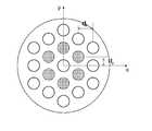
도 6a 는 본 발명에 의한 FTEP를 형성하기 위한 유전체봉의 육각 배열 구조의 일실시예 상측면도.Figure 6a is a top side view of an embodiment of a hexagonal arrangement of dielectric rods for forming the FTEP according to the present invention.
도 6b 는 본 발명에 의한 FTEP를 형성하기 위한 유전체봉의 육각 배열 구조의 일실시예 단면도.Figure 6b is a cross-sectional view of an embodiment of a hexagonal arrangement of dielectric rods for forming FTEP according to the present invention.
도 6c 는 본 발명의 일실시예에 따른 원형 도파관에 의해 여기되는 FTEP를 형성하기 위한 유전체봉의 육각 배열 구조의 상측면도.6C is a top side view of a hexagonal arrangement of dielectric rods for forming FTEP excited by a circular waveguide, in accordance with one embodiment of the present invention;
*도면의 주요부분에 대한 부호의 설명* Explanation of symbols for main parts of the drawings
610 : 중심 소자 620 : 제 1 링 소자610: center element 620: first ring element
630 : 제2 링 소자 640 : 원형 도파관 배열 지지물630: second ring element 640: circular waveguide array support
본 발명은 플랫-탑 엘리먼트 패턴(Flat-Topped Element Pattern ; 이하 'FTEP'라고 함)을 형성하기 위한 유전체봉(dielectric rod)의 배열 구조에 관한 것으로, 더욱 상세하게는 유전체봉을 중심에 두고 주위에 일정한 크기의 유전체봉을 정육각형의 꼭지점에 평면적으로 배열하여 중심 급전 소자와 주변 인접 소자들의 자연 발생적인 강한 전자파 상호결합(Mutual coupling)에 의해 넓은 빔 스캐닝 범위와 균일한 전기적 성능을 가지는, FTEP를 형성하기 위한 유전체봉의 육각 배열 구조에 관한 것이다.The present invention relates to an arrangement of dielectric rods for forming a flat-topped element pattern (hereinafter referred to as 'FTEP'), and more particularly, to a peripheral structure centered on the dielectric rod. FTEP has a wide beam scanning range and uniform electrical performance due to the naturally-occurring strong electromagnetic coupling of the center feeder and its neighboring neighbors by arranging dielectric rods of uniform size at the vertices of the regular hexagon. A hexagonal arrangement of dielectric rods for forming.
한국공개특허 제2003-0071996호(FTEP를 형성하기 위한 이차원 다층 원형 방사 배열 구조)에 의하면, 일반적으로 위상 제어 소자는 위상 배열 안테나(Phased array antenna)의 개발에 있어서 가장 핵심적이고 고가인 부품으로써, 안테나 배열 이득, 사이드 로브 레벨(Side lobe level), 섹터 빔 스캔 요구 규격에 따라 장착되어야 하는 개수가 결정된다. 여기서 안테나 배열 이득, 사이드 로브 레벨 규격은 배열 개구면 모양이나 크기를 결정하는데 사용되고, 섹터 빔 스캔 요구 규격은 배열 소자 간격의 크기를 결정하는데 사용된다.According to Korean Patent Laid-Open Publication No. 2003-0071996 (two-dimensional multilayer circular radiating array structure for forming FTEP), a phase control element is generally the most important and expensive component in the development of a phased array antenna. The number of antennas to be mounted depends on antenna array gain, side lobe level, and sector beam scan requirements. Here, antenna array gain and side lobe level specifications are used to determine array aperture shape and size, and sector beam scan requirement specifications are used to determine array element spacing size.
또한, 종래의 일반적인 방법에 있어서, 위상 제어 소자의 배열을 설계할 시, 광범위한 빔 스캐닝을 위하여 배열 인자에 의한 그레이팅 로브(Grating lobe)가 실 공간(real space)에 존재하지 않도록 위상 제어 소자의 최대 배열 간격을 결정하였다.In addition, in the conventional general method, when designing the arrangement of the phase control element, the maximum of the phase control element so that the grating lobe due to the array factor does not exist in the real space for a wide range of beam scanning. Array spacing was determined.
반면에, FTEP 기술은 상대적으로 작은 빔 스캐닝 범위(±(5˚내지 25˚))를 갖기 때문에, 배열 인자에 의한 그레이팅 로브(Grating lobe)가 실 공간(real space)에 존재하지 않도록 최대 배열 간격을 결정할 수 있고, FTEP의 사이드 로브 특성에 의해 그레이팅 로브를 억압하는 특징이 있다. 이에 따라 종래의 일반적인 방법에 비해, 위상 제어 소자의 소자간 간격이 상대적으로 증가하여 위상 제어 소자 수를 최소로 할 수 있다. 예를 들어, 20˚의 원추형 빔 스캐닝을 요구하는 위상 배열 설계에서 상술한 FTEP의 기술을 사용할 경우, 일반적인 방법에 비해 위상 제어 소자 수를 1/11로 감소시킬 수 있다. 여기서, 요구되는 스캐닝 범위 내에서 FTEP를 형성하기 위해서는, 배열 개구면 진폭 분포 특성이, 겹쳐진 서브 배열(Overlapped subarray) 특성을 가짐과 동시에 1차원 배열의 경우


종래에는 상술한 배열 특성을 얻기 위하여 아래와 같이 크게 다섯 가지의 구조가 사용되었다.Conventionally, five structures are largely used as follows to obtain the above-described arrangement characteristics.
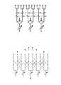
도 1a 내지 도 1h 는 종래기술에 따른 수동 다단자망을 갖는 배열구조도이다. 도 1a 에 도시된 바와 같이, 수동 다단자망을 갖는 배열 구조는, 위상 배열 안테나 시스템의 빔성형 및 빔조향 블록에서 입출력 신호간에 요구되는 위상차를 제공하는 위상 천이기(110), 안테나 배열 소자(120), 상기 위상 천이기(110)와 배열 소자(120) 사이에 삽입되어 FTEP를 위한 요구 진폭 및 위상 분포를 형성하는 다단자망(Multiport network, 130)을 포함하고 있다. 그 밖에 다양한 다단자 망의 실시예가 도 1b 내지 1h 에 도시되어 있다. 그러나, 이와 같은 배열 구조는 이차원 빔 스캐닝 시 급전망이 복잡하여 효율이 떨어지고, 부피가 큰 것과 동시에 무게도 무거우며, 시스템 가격이 높다는 등의 문제점이 있다.1A to 1H are arrangement diagrams having a passive multi-terminal network according to the prior art. As shown in FIG. 1A, an array structure having a passive multi-terminal network includes a
도 2a 는 종래의 전계(E)-평면에서의 선형 배열 스캐닝을 나타낸 구조도이고, 도 2b 는 종래의 자계(H)-평면에서의 선형 배열 스캐닝을 나타낸 구조도이다. 이중 모드 도파관은 공통된 벽을 가지기 때문에 도파관 벽에서의 슬롯들을 통해 필요한 모드들을 여기할 수 있도록 하여 안테나 배열 설계를 간소화시킬 수 있는 장점이 있다. 도 2a 는 전계(E)-평면에서의 선형 배열 스캐닝을 나타낸 구조도이고, 도 2b는 자계(H)-평면에서의 선형 배열 스캐닝을 나타낸 구조도로서, 소정의 직경(a0)을 가지고 마이크로파를 필터링하여 통과시키는 단일 모드 도파관(210, 211), 소정의 직경(at) 및 길이(ht)를 가지고 단일 모드 도파관(210, 211)과 후술하는 이중 모드 도파관(230, 231) 사이의 임피던스 정합을 제공하는 임피던스 정합 도파관(220, 221), 및 이중 슬롯을 통해 전력을 상호결합하는 이중 모드 도파관(230, 231)을 포함한다. 그러나, 이러한 구조에서는 상대적으로 작은 대역폭 및 작은 빔 스캐닝 범위를 가지며, 일차원의 응용에 한정되는 문제점이 있다.2A is a structural diagram showing a linear array scanning in a conventional electric field (E) -plane, and FIG. 2B is a structural diagram showing a linear array scanning in a conventional magnetic field (H) -plane. Since dual mode waveguides have a common wall, they have the advantage of simplifying antenna array design by allowing the desired modes to be excited through slots in the waveguide wall. 2A is a structural diagram showing linear array scanning in the electric field (E) -plane, and FIG. 2B is a structural diagram showing linear array scanning in the magnetic field (H) -plane, and filtering microwaves with a predetermined diameter (a0 ). Impedance matching between the
도 3 은 앞서 언급했던 한국공개특허 제2003-0071996호(FTEP를 형성하기 위한 이차원 다층 원형 방사 배열 구조)에서 제안된 것으로 이차원 다층 원형 방사 배열 구조이다. 이차원 다층 원형 방사 배열 구조는, 도 3에 도시된 바와 같이, 일정한 크기의 원형 도체 디스크들을 정삼각형 격자를 반복 단위로 하여 평면적으로 배열하고, 또한 전파 진행 방향으로 일정한 간격의 다층으로 적층함으로써, 중심 급전 소자와 주변 인접 소자들의 자연 발생적인 상호 전자파 결합을 이용하는 것이다. 이 구조는 디스크를 적층형으로 구현해야 하므로 상대적으로 제작이 복잡하고, 디스크의 배열 및 적층시 성공적인 동기가 요구된다.3 is a two-dimensional multilayer circular radiation array structure proposed in Korean Patent Laid-Open Publication No. 2003-0071996 (two-dimensional multilayer circular radiation array structure for forming FTEP). In the two-dimensional multilayer circular radiating arrangement structure, as shown in FIG. 3, circular conductive disks of constant size are arranged in a planar manner by using an equilateral triangle lattice as repeating units, and also stacked in multiple layers of uniform intervals in the propagation propagation direction, thereby providing a central feed. It takes advantage of the naturally occurring mutual electromagnetic coupling of the device and its surrounding neighbors. This structure is relatively complicated to manufacture since the disks must be stacked, and successful synchronization is required when arranging and stacking the disks.
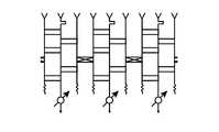
도 4a 내지 4c 는 종래의 주름진 도파관 배열 구조도이다. 주름진 도파관 배열 구조는, 도 4a 및 4b 에 도시된 바와 같이, 외부에서 입력되는 신호를 수신하는 배열 소자(410, 411), 리액티브 임피던스(reactive impedance)를 갖고 상기 배열 소자(410, 411)에 반사 터미네이션(reflective termination)의 기능을 하는 리액티브 부하(420, 421)를 포함한다. 여기서, 단지 몇 개의 배열 소자만 위상 제어 소자에 직접 연결되고, 나머지 대부분의 방사 소자는 리액티브 부하에 연결된다. 이러한 리액티브 부하가 부착된 수동 방사 소자에서의 방사는 위상 제어 소자에 직접 연결된 능동 방사 소자와의 상호결합 및 리액티브 부하의 반사에 의해 이루어지며, 도 4a 및 4b 에 하나의 반복단위(b)에서 이루어지는 반사 과정이 도시되어 있다. 한편, 도 4c 에는 리액티브 부하를 위해 다양한 도파관 길이를 갖는 주름진 배열 구조가 도시되어 있다. FTEP 형성을 위해서는 필요에 따라 더욱 충분한 결합이 요구되는데, 이를 위해 개구면 위에 추가 수동 산란체를 설치할 수 있다. 그러나 이러한 반사적 부하 배열 구조, 즉 주름진 도파관 구조를 이용한 배열 구조는, 안테나 소자 배열 간격이 0.7 내지 0.85λ 이므로 위상 천이기가 다수개 필요하고, 3% 이상의 배열 안테나 설계가 불가능하며, 부피가 큰 것과 동시에 무게도 무거우며, 시스템 가격이 높은 문제점이 있다.4A-4C are conventional corrugated waveguide arrangements. The corrugated waveguide array structure has
도 5a 및 5b 는 종래의 유사 광학망을 이용한 배열 구조도이고, 도 5c 는 종래의 방향성 결합기와 그 유사 광학적 등가를 나타낸 예시도이다. 공간 물체 추적을 위해서는 주로 광범위의 기계적 빔조향 장치와 협대역의 전자 빔조향 장치가 혼합되어 사용되는데, 이와 같이 전자적으로 빔 스캐닝 범위가 아주 좁은 FTEP 형성을 위해서 상기 도 1a 내지 1h 에 도시된 바와 같은 다단자 망을 사용할 수 있다. 그러나, 이를 위해서는 상호 방사 소자 간의 간격이 멀어, 다단자망 전송선로 길이를 증가시키게 되고, 이로 인해 상당히 큰 저항성 손실을 초래하는 문제점이 있었다.5A and 5B are arrangement diagrams using a conventional optical network, and FIG. 5C is an exemplary view showing a conventional directional coupler and its optical equivalent. For the tracking of spatial objects, a wide range of mechanical beam steering devices and narrow-band electron beam steering devices are used. As shown in FIGS. 1A to 1H, the FTEP is formed to have a very narrow beam scanning range electronically. Multiterminal networks can be used. However, for this purpose, the distance between the mutual radiating elements is far, which increases the length of the multi-terminal transmission line, resulting in a significant loss of resistance.
유사 광학망을 이용한 배열 구조는 이러한 단점을 극복하기 위한 것으로, 도 5a 및 5b 에 도시된 바와 같이 두 종류의 유사 광학망을 사용할 수 있다. 도 5c 는 유전체 플레이트, 와이어 격자와 같은 반투명 스크린을 이용하여 방향성 결합기(directional coupler)와 유사한 특성을 얻을 수 있음을 나타내고 있다. 그러나, 이러한 유사 광학망을 이용한 배열 구조는 대규모 배열 안테나의 아주 좁은 빔 스캐닝에만 제한적으로 적용할 수 있다는 문제점이 있다.The arrangement structure using the similar optical net is to overcome this disadvantage, and two types of similar optical nets may be used as shown in FIGS. 5A and 5B. 5C shows that a semi-transparent screen such as a dielectric plate, a wire grating can be used to obtain properties similar to a directional coupler. However, there is a problem that such an arrangement using a similar optical network can be limitedly limited to very narrow beam scanning of a large array antenna.
상기한 바와 같은 문제점을 해결하기 위하여 제안된 본 발명은, 유전체봉을 중심에 두고 주위에 일정한 크기의 유전체봉을 정육각형의 꼭지점에 평면적으로 배열하여 중심 급전 소자와 주변 인접 소자들의 자연 발생적인 강한 전자파 상호결합(Mutual coupling)에 의해 넓은 빔 스캐닝 범위와 균일한 전기적 성능을 가지는, FTEP를 형성하기 위한 유전체봉의 육각 배열 구조를 제공하는데 그 목적이 있다.
In order to solve the above problems, the present invention proposes a planar arrangement of dielectric rods of a constant size centered around the dielectric rods at the vertices of a regular hexagon, thereby generating a strong electromagnetic wave generated naturally from the center feeding element and neighboring neighboring elements. It is an object of the present invention to provide a hexagonal array structure of dielectric rods for forming FTEP having a wide beam scanning range and uniform electrical performance by mutual coupling.
상기 목적을 달성하기 위한 본 발명은, 플랫-탑 엘리먼트 패턴(FTEP)를 형성하는 유전체봉의 배열 구조에 있어서, 기본 모드의 편파 신호를 급전하여, 제1 유전체봉을 통해 진행파를 형성하여 방사함으로써, 유전체봉간에 상호 전자파 결합을 통하여 FTEP의 단위 방사 패턴을 형성하기 위한 중심 소자; 상기 중심 소자를 중심점으로 하는 정육각형의 꼭지점 상에 배치되어, 제2 유전체봉을 통해 상기 중심 소자의 제1 유전체봉과 전자파 상호결합하여 상기 단위 방사 패턴을 형성하기 위한 6(N-1)(N은 2이상의 자연수임)개의 링 소자; 및 상기 중심 소자, 상기 6(N-1)개의 링 소자를 지지하기 위한 원형 도파관 배열 지지 수단을 포함하여 이루어진 것을 특징으로 한다.
또한, 본 발명은, 플랫-탑 엘리먼트 패턴(FTEP)를 형성하는 유전체봉의 배열 구조에 있어서, 기본 모드의 편파 신호를 급전하여, 제1 유전체봉을 통해 진행파를 형성하여 방사함으로써, 유전체봉간에 상호 전자파 결합을 통하여 FTEP의 단위 방사 패턴을 형성하기 위한 중심 소자; 상기 중심 소자를 중심점으로 하는 제1 정육각형의 꼭지점 상에 배치되어, 제2 유전체봉을 통해 상기 중심 소자의 제1 유전체봉과 전자파 상호결합하여 상기 단위 방사 패턴을 형성하기 위한 6(N-1)(N은 2이상의 자연수임)개의 링 소자; 상기 중심 소자를 중심점으로 하여 상기 제1 정육각형을 포함하는 제2 정육각형의 꼭지점 상에 배치되며, 상기 N개의 링 소자 중 하나 혹은 두 개를 꼭지점으로 하는 정삼각형 격자의 나머지 꼭지점에 동일한 간격으로 배치되어, 제3 유전체봉을 통해 인접한 링 소자의 유전체봉과 전자파 상호결합하여 방사 패턴을 형성하기 위한 6N개의 링 소자; 및 상기 중심 소자, 상기 6(N-1)개의 링 소자, 상기 6N개의 링 소자를 지지하기 위한 원형 도파관 배열 지지 수단을 포함하여 이루어진 것을 특징으로 한다.The present invention for achieving the above object, in the array structure of the dielectric rod forming the flat-top element pattern (FTEP), by supplying the polarization signal of the basic mode, by forming a traveling wave through the first dielectric rod, A center element for forming a unit radiation pattern of FTEP through mutual electromagnetic coupling between dielectric bars; 6 (N-1) (N is disposed on a vertex of a regular hexagon having the center element as a center point to form the unit radiation pattern by electromagnetic coupling with the first dielectric rod of the center element through a second dielectric rod. Two or more natural numbers) ring elements; And circular waveguide array support means for supporting the center element and the 6 (N-1) ring elements.
In addition, the present invention, in the array structure of the dielectric rods forming the flat-top element pattern (FTEP), the polarization signal of the basic mode is fed to form a radiation wave through the first dielectric rod to radiate, thereby mutually A center element for forming a unit radiation pattern of the FTEP through electromagnetic wave coupling; 6 (N-1) disposed on a vertex of a first regular hexagon having the center element as a center point, for forming the unit radiation pattern by electromagnetic coupling with the first dielectric rod of the center element through a second dielectric rod; N is two or more natural numbers) ring elements; Disposed on the vertex of the second regular hexagon including the first regular hexagon with the center element as the center point, and disposed at the same intervals at the remaining vertices of the equilateral triangle lattice having one or two of the N ring elements as vertices, 6N ring elements for electromagnetic radiation coupling with the dielectric rods of adjacent ring elements through a third dielectric rod to form a radiation pattern; And circular waveguide arrangement supporting means for supporting the center element, the 6 (N-1) ring elements, and the 6N ring elements.
삭제delete
삭제delete
삭제delete
삭제delete
삭제delete
상술한 목적, 특징들 및 장점은 첨부된 도면과 관련한 다음의 상세한 설명을 통하여 보다 분명해 질 것이다. 이하, 첨부된 도면을 참조하여 본 발명에 따른 바람직한 일실시예를 상세히 설명한다.The above objects, features and advantages will become more apparent from the following detailed description taken in conjunction with the accompanying drawings. Hereinafter, exemplary embodiments of the present invention will be described in detail with reference to the accompanying drawings.
도 6a 는 본 발명에 의한 FTEP를 형성하기 위한 유전체봉의 육각 배열 구조의 일실시예 상측면도이고, 도 6b 는 본 발명에 의한 FTEP를 형성하기 위한 유전체봉의 육각 배열 구조의 일실시예 단면도이며, 도 6c 는 본 발명의 일실시예에 따른 원형 도파관에 의해 여기되는 FTEP를 형성하기 위한 유전체봉의 육각 배열 구조의 상측면도이다.Figure 6a is a top side view of an embodiment of the hexagonal arrangement of the dielectric rods for forming the FTEP according to the present invention, Figure 6b is a cross-sectional view of one embodiment of the hexagonal arrangement of the dielectric rods for forming the FTEP according to the present invention, Figure 6c is a top side view of a hexagonal arrangement of dielectric rods for forming FTEP excited by a circular waveguide according to one embodiment of the present invention.
본 발명의 FTEP를 형성하기 위한 유전체봉 육각 배열 구조는 중심 소자(610), 6개의 제 1 링 소자(620), 12개의 제 2 링 소자(630), 원형 도파관 배열 지지물(640)을 포함한다.The dielectric rod hexagon array structure for forming the FTEP of the present invention includes a
상기 중심 소자(610) 및 6개의 제 1 링 소자(620)에 기본 모드의 신호를 편 파기(612)를 통하여 급전하면, 12개의 제 2 링 소자(630)와 전자파 상호결합을 통하여 안테나 개구면에 요구사항에 적합한 전류 분포를 형성하게 되며, 원역장에서 FTEP 방사 패턴을 형성한다. 여기서 중심 소자(610)는, 입력 원형 동축케이블(611), 편파기(612), 방사소자인 유전체봉(613)을 포함하고 있다.When the signal of the basic mode is supplied to the
상기 중심 소자(610) 내에 장착된 입력 원형 동축케이블(611)은 입력 신호를 급전하는 역할을 하며, 또한 상기 중심 소자(610) 내에 장착된 편파기(612)는 원형 도파관(즉, 입력 원형 동축케이블(611)) 내에 위치한 얇은 유전체 판으로 요구하는 편파를 형성하며, 유전체봉(613)은 진행파를 형성하여 방사하는 역할을 하며, 전자파 상호결합을 통해 FTEP를 이루는 단위 방사 패턴을 만드는 역할을 한다.The input circular
중심소자(610) 및 각각의 제 1 링 소자(620)는, 제 2 링 소자(630)와 전자파 상호결합하여 FTEP 단위 방사 패턴을 만드는 역할을 하며, 제 1 링 소자(620)는 상기 중심 소자(610)를 하나의 중심점으로 하여 주위에 정육각형의 모양으로 6개가 장착되는데, 그 간격은 dx , dy 이고, 이에 따라 각각의 xy좌표 상에서의 위치는 (dx, dy), (dx, -dy), (-dx, dy), (-dx, -dy) (0, 2dy), (0, -2dy)이며, 제 2 링 소자(630)는 제 1 링 소자 하나 또는 두 개를 꼭지점으로 하는 정삼각형 격자의 나머지 꼭지점 상에 장착되어 중심소자(610)로부터 2번째 정육각형의 모양을 형성하며, 각각의 xy 좌표상에서의 위치는 (2dx, 0), (-2dx, 0), (2dx, 2dy), (2dx, -2dy), (dx, 3dy), (dx, -3dy), (0, 4dy), (0, -4dy) (0, 2dy), (0, -2dy), (-dx, 3dy), (-dx, -3dy)이다(도 6c에 도시됨).The
급전되는 소자인 상기 중심소자(610)와 상기 6개의 제 1 링 소자(620)에는 편파의 발생을 위해 편파기(612)가 포함되며, 12개의 제 2 링 소자(630)에는 편파기가 포함되어지지 않는다.The
이상에서 설명한 본 발명은, 본 발명이 속하는 기술분야에서 통상의 지식을 가진 자에 있어 본 발명의 기술적 사상을 벗어나지 않는 범위내에서 여러 가지 치환, 변형 및 변경이 가능하므로 전술한 실시예 및 첨부된 도면에 한정되는 것이 아니다.The present invention described above is capable of various substitutions, modifications, and changes without departing from the spirit of the present invention for those skilled in the art to which the present invention pertains, and the above-described embodiments and accompanying It is not limited to the drawing.
상기한 바와 같은 본 발명은, FTEP를 형성하기 위한 유전체봉 육각 배열 구조를 통해 그레이팅 로브를 억압하여 방사 소자의 수를 줄임으로써, 소자수 증가에 따른 비용을 줄이는 동시에 급전 손실을 감소시켜, 상대적으로 넓은 빔 스캐닝에 적용될 수 있도록 하는 효과가 있다.The present invention as described above, by reducing the number of radiating elements by suppressing the grating lobe through the dielectric rod hexagon array structure for forming the FTEP, while reducing the cost of increasing the number of elements, while reducing the feed loss, There is an effect that can be applied to wide beam scanning.
또한, 본 발명은 웨이브가이드에 일정한 크기의 유전체봉을 고정시키는 것으로 밀리미터파 대역(약 10GHz 이상)에서 상대적으로 제작이 용이하고 가벼운 등의 다양한 효과가 있다.In addition, the present invention has a variety of effects, such as relatively easy to manufacture and light in the millimeter wave band (about 10GHz or more) by fixing a dielectric rod of a predetermined size to the wave guide.
Claims (6)
Translated fromKoreanPriority Applications (2)
| Application Number | Priority Date | Filing Date | Title |
|---|---|---|---|
| KR1020030098389AKR100574228B1 (en) | 2003-12-27 | 2003-12-27 | Hexagonal arrangement of dielectric rods to form flat-top element patterns |
| US11/023,682US7167139B2 (en) | 2003-12-27 | 2004-12-27 | Hexagonal array structure of dielectric rod to shape flat-topped element pattern |
Applications Claiming Priority (1)
| Application Number | Priority Date | Filing Date | Title |
|---|---|---|---|
| KR1020030098389AKR100574228B1 (en) | 2003-12-27 | 2003-12-27 | Hexagonal arrangement of dielectric rods to form flat-top element patterns |
Publications (2)
| Publication Number | Publication Date |
|---|---|
| KR20050066904A KR20050066904A (en) | 2005-06-30 |
| KR100574228B1true KR100574228B1 (en) | 2006-04-26 |
Family
ID=34698619
Family Applications (1)
| Application Number | Title | Priority Date | Filing Date |
|---|---|---|---|
| KR1020030098389AExpired - Fee RelatedKR100574228B1 (en) | 2003-12-27 | 2003-12-27 | Hexagonal arrangement of dielectric rods to form flat-top element patterns |
Country Status (2)
| Country | Link |
|---|---|
| US (1) | US7167139B2 (en) |
| KR (1) | KR100574228B1 (en) |
Families Citing this family (181)
| Publication number | Priority date | Publication date | Assignee | Title |
|---|---|---|---|---|
| US7474262B2 (en)* | 2005-07-01 | 2009-01-06 | Delphi Technologies, Inc. | Digital beamforming for an electronically scanned radar system |
| US8126477B2 (en)* | 2005-07-07 | 2012-02-28 | Qualcomm Incorporated | Methods and devices for interworking of wireless wide area networks and wireless local area networks or wireless personal area networks |
| US8364148B2 (en) | 2005-07-07 | 2013-01-29 | Qualcomm Incorporated | Methods and devices for interworking of wireless wide area networks and wireless local area networks or wireless personal area networks |
| US8311543B2 (en)* | 2005-07-07 | 2012-11-13 | Qualcomm Incorporated | Methods and devices for interworking of wireless wide area networks and wireless local area networks or wireless personal area networks |
| US9130602B2 (en) | 2006-01-18 | 2015-09-08 | Qualcomm Incorporated | Method and apparatus for delivering energy to an electrical or electronic device via a wireless link |
| US8447234B2 (en)* | 2006-01-18 | 2013-05-21 | Qualcomm Incorporated | Method and system for powering an electronic device via a wireless link |
| US9774086B2 (en)* | 2007-03-02 | 2017-09-26 | Qualcomm Incorporated | Wireless power apparatus and methods |
| US9124120B2 (en) | 2007-06-11 | 2015-09-01 | Qualcomm Incorporated | Wireless power system and proximity effects |
| KR20130036071A (en)* | 2007-08-09 | 2013-04-09 | 퀄컴 인코포레이티드 | Resonant antenna system with high q factor |
| CN101803109A (en) | 2007-09-13 | 2010-08-11 | 高通股份有限公司 | Maximizing power yield from wireless power magnetic resonators |
| WO2009039113A1 (en)* | 2007-09-17 | 2009-03-26 | Nigel Power, Llc | Transmitters and receivers for wireless energy transfer |
| US7639171B2 (en)* | 2007-09-27 | 2009-12-29 | Delphi Technologies, Inc. | Radar system and method of digital beamforming |
| JP5362733B2 (en)* | 2007-10-11 | 2013-12-11 | クゥアルコム・インコーポレイテッド | Wireless power transfer using a magneto-mechanical system |
| US8629576B2 (en)* | 2008-03-28 | 2014-01-14 | Qualcomm Incorporated | Tuning and gain control in electro-magnetic power systems |
| US20090273242A1 (en)* | 2008-05-05 | 2009-11-05 | Nigelpower, Llc | Wireless Delivery of power to a Fixed-Geometry power part |
| US20090299918A1 (en)* | 2008-05-28 | 2009-12-03 | Nigelpower, Llc | Wireless delivery of power to a mobile powered device |
| US9113347B2 (en) | 2012-12-05 | 2015-08-18 | At&T Intellectual Property I, Lp | Backhaul link for distributed antenna system |
| US10009065B2 (en) | 2012-12-05 | 2018-06-26 | At&T Intellectual Property I, L.P. | Backhaul link for distributed antenna system |
| US9999038B2 (en) | 2013-05-31 | 2018-06-12 | At&T Intellectual Property I, L.P. | Remote distributed antenna system |
| US9525524B2 (en) | 2013-05-31 | 2016-12-20 | At&T Intellectual Property I, L.P. | Remote distributed antenna system |
| US9601267B2 (en) | 2013-07-03 | 2017-03-21 | Qualcomm Incorporated | Wireless power transmitter with a plurality of magnetic oscillators |
| EP2840650B1 (en)* | 2013-08-24 | 2018-12-26 | HENSOLDT Sensors GmbH | Three-dimensional antenna array |
| US8897697B1 (en) | 2013-11-06 | 2014-11-25 | At&T Intellectual Property I, Lp | Millimeter-wave surface-wave communications |
| US9209902B2 (en) | 2013-12-10 | 2015-12-08 | At&T Intellectual Property I, L.P. | Quasi-optical coupler |
| US9692101B2 (en) | 2014-08-26 | 2017-06-27 | At&T Intellectual Property I, L.P. | Guided wave couplers for coupling electromagnetic waves between a waveguide surface and a surface of a wire |
| US9768833B2 (en) | 2014-09-15 | 2017-09-19 | At&T Intellectual Property I, L.P. | Method and apparatus for sensing a condition in a transmission medium of electromagnetic waves |
| US10063280B2 (en) | 2014-09-17 | 2018-08-28 | At&T Intellectual Property I, L.P. | Monitoring and mitigating conditions in a communication network |
| US9628854B2 (en) | 2014-09-29 | 2017-04-18 | At&T Intellectual Property I, L.P. | Method and apparatus for distributing content in a communication network |
| US9615269B2 (en) | 2014-10-02 | 2017-04-04 | At&T Intellectual Property I, L.P. | Method and apparatus that provides fault tolerance in a communication network |
| US9685992B2 (en) | 2014-10-03 | 2017-06-20 | At&T Intellectual Property I, L.P. | Circuit panel network and methods thereof |
| US9503189B2 (en) | 2014-10-10 | 2016-11-22 | At&T Intellectual Property I, L.P. | Method and apparatus for arranging communication sessions in a communication system |
| US9973299B2 (en) | 2014-10-14 | 2018-05-15 | At&T Intellectual Property I, L.P. | Method and apparatus for adjusting a mode of communication in a communication network |
| US9762289B2 (en) | 2014-10-14 | 2017-09-12 | At&T Intellectual Property I, L.P. | Method and apparatus for transmitting or receiving signals in a transportation system |
| US9577306B2 (en) | 2014-10-21 | 2017-02-21 | At&T Intellectual Property I, L.P. | Guided-wave transmission device and methods for use therewith |
| US9769020B2 (en) | 2014-10-21 | 2017-09-19 | At&T Intellectual Property I, L.P. | Method and apparatus for responding to events affecting communications in a communication network |
| US9564947B2 (en) | 2014-10-21 | 2017-02-07 | At&T Intellectual Property I, L.P. | Guided-wave transmission device with diversity and methods for use therewith |
| US9312919B1 (en) | 2014-10-21 | 2016-04-12 | At&T Intellectual Property I, Lp | Transmission device with impairment compensation and methods for use therewith |
| US9520945B2 (en) | 2014-10-21 | 2016-12-13 | At&T Intellectual Property I, L.P. | Apparatus for providing communication services and methods thereof |
| US9627768B2 (en) | 2014-10-21 | 2017-04-18 | At&T Intellectual Property I, L.P. | Guided-wave transmission device with non-fundamental mode propagation and methods for use therewith |
| US9780834B2 (en) | 2014-10-21 | 2017-10-03 | At&T Intellectual Property I, L.P. | Method and apparatus for transmitting electromagnetic waves |
| US9653770B2 (en) | 2014-10-21 | 2017-05-16 | At&T Intellectual Property I, L.P. | Guided wave coupler, coupling module and methods for use therewith |
| US9544006B2 (en) | 2014-11-20 | 2017-01-10 | At&T Intellectual Property I, L.P. | Transmission device with mode division multiplexing and methods for use therewith |
| US9800327B2 (en) | 2014-11-20 | 2017-10-24 | At&T Intellectual Property I, L.P. | Apparatus for controlling operations of a communication device and methods thereof |
| US9680670B2 (en) | 2014-11-20 | 2017-06-13 | At&T Intellectual Property I, L.P. | Transmission device with channel equalization and control and methods for use therewith |
| US9997819B2 (en) | 2015-06-09 | 2018-06-12 | At&T Intellectual Property I, L.P. | Transmission medium and method for facilitating propagation of electromagnetic waves via a core |
| US10243784B2 (en) | 2014-11-20 | 2019-03-26 | At&T Intellectual Property I, L.P. | System for generating topology information and methods thereof |
| US9954287B2 (en) | 2014-11-20 | 2018-04-24 | At&T Intellectual Property I, L.P. | Apparatus for converting wireless signals and electromagnetic waves and methods thereof |
| US9742462B2 (en) | 2014-12-04 | 2017-08-22 | At&T Intellectual Property I, L.P. | Transmission medium and communication interfaces and methods for use therewith |
| US9461706B1 (en) | 2015-07-31 | 2016-10-04 | At&T Intellectual Property I, Lp | Method and apparatus for exchanging communication signals |
| US10009067B2 (en) | 2014-12-04 | 2018-06-26 | At&T Intellectual Property I, L.P. | Method and apparatus for configuring a communication interface |
| US9654173B2 (en) | 2014-11-20 | 2017-05-16 | At&T Intellectual Property I, L.P. | Apparatus for powering a communication device and methods thereof |
| US10340573B2 (en) | 2016-10-26 | 2019-07-02 | At&T Intellectual Property I, L.P. | Launcher with cylindrical coupling device and methods for use therewith |
| US10144036B2 (en) | 2015-01-30 | 2018-12-04 | At&T Intellectual Property I, L.P. | Method and apparatus for mitigating interference affecting a propagation of electromagnetic waves guided by a transmission medium |
| US9876570B2 (en) | 2015-02-20 | 2018-01-23 | At&T Intellectual Property I, Lp | Guided-wave transmission device with non-fundamental mode propagation and methods for use therewith |
| US9749013B2 (en) | 2015-03-17 | 2017-08-29 | At&T Intellectual Property I, L.P. | Method and apparatus for reducing attenuation of electromagnetic waves guided by a transmission medium |
| US10224981B2 (en) | 2015-04-24 | 2019-03-05 | At&T Intellectual Property I, Lp | Passive electrical coupling device and methods for use therewith |
| US9705561B2 (en) | 2015-04-24 | 2017-07-11 | At&T Intellectual Property I, L.P. | Directional coupling device and methods for use therewith |
| US9793954B2 (en) | 2015-04-28 | 2017-10-17 | At&T Intellectual Property I, L.P. | Magnetic coupling device and methods for use therewith |
| US9948354B2 (en) | 2015-04-28 | 2018-04-17 | At&T Intellectual Property I, L.P. | Magnetic coupling device with reflective plate and methods for use therewith |
| US9871282B2 (en) | 2015-05-14 | 2018-01-16 | At&T Intellectual Property I, L.P. | At least one transmission medium having a dielectric surface that is covered at least in part by a second dielectric |
| US9748626B2 (en) | 2015-05-14 | 2017-08-29 | At&T Intellectual Property I, L.P. | Plurality of cables having different cross-sectional shapes which are bundled together to form a transmission medium |
| US9490869B1 (en) | 2015-05-14 | 2016-11-08 | At&T Intellectual Property I, L.P. | Transmission medium having multiple cores and methods for use therewith |
| US10679767B2 (en) | 2015-05-15 | 2020-06-09 | At&T Intellectual Property I, L.P. | Transmission medium having a conductive material and methods for use therewith |
| US10650940B2 (en) | 2015-05-15 | 2020-05-12 | At&T Intellectual Property I, L.P. | Transmission medium having a conductive material and methods for use therewith |
| US9917341B2 (en) | 2015-05-27 | 2018-03-13 | At&T Intellectual Property I, L.P. | Apparatus and method for launching electromagnetic waves and for modifying radial dimensions of the propagating electromagnetic waves |
| US10154493B2 (en) | 2015-06-03 | 2018-12-11 | At&T Intellectual Property I, L.P. | Network termination and methods for use therewith |
| US10812174B2 (en) | 2015-06-03 | 2020-10-20 | At&T Intellectual Property I, L.P. | Client node device and methods for use therewith |
| US10103801B2 (en) | 2015-06-03 | 2018-10-16 | At&T Intellectual Property I, L.P. | Host node device and methods for use therewith |
| US9866309B2 (en) | 2015-06-03 | 2018-01-09 | At&T Intellectual Property I, Lp | Host node device and methods for use therewith |
| US9912381B2 (en) | 2015-06-03 | 2018-03-06 | At&T Intellectual Property I, Lp | Network termination and methods for use therewith |
| US10348391B2 (en) | 2015-06-03 | 2019-07-09 | At&T Intellectual Property I, L.P. | Client node device with frequency conversion and methods for use therewith |
| US9913139B2 (en) | 2015-06-09 | 2018-03-06 | At&T Intellectual Property I, L.P. | Signal fingerprinting for authentication of communicating devices |
| US10142086B2 (en) | 2015-06-11 | 2018-11-27 | At&T Intellectual Property I, L.P. | Repeater and methods for use therewith |
| US9608692B2 (en) | 2015-06-11 | 2017-03-28 | At&T Intellectual Property I, L.P. | Repeater and methods for use therewith |
| US9820146B2 (en) | 2015-06-12 | 2017-11-14 | At&T Intellectual Property I, L.P. | Method and apparatus for authentication and identity management of communicating devices |
| US9667317B2 (en) | 2015-06-15 | 2017-05-30 | At&T Intellectual Property I, L.P. | Method and apparatus for providing security using network traffic adjustments |
| US9509415B1 (en) | 2015-06-25 | 2016-11-29 | At&T Intellectual Property I, L.P. | Methods and apparatus for inducing a fundamental wave mode on a transmission medium |
| US9640850B2 (en) | 2015-06-25 | 2017-05-02 | At&T Intellectual Property I, L.P. | Methods and apparatus for inducing a non-fundamental wave mode on a transmission medium |
| US9865911B2 (en) | 2015-06-25 | 2018-01-09 | At&T Intellectual Property I, L.P. | Waveguide system for slot radiating first electromagnetic waves that are combined into a non-fundamental wave mode second electromagnetic wave on a transmission medium |
| US9722318B2 (en) | 2015-07-14 | 2017-08-01 | At&T Intellectual Property I, L.P. | Method and apparatus for coupling an antenna to a device |
| US10170840B2 (en) | 2015-07-14 | 2019-01-01 | At&T Intellectual Property I, L.P. | Apparatus and methods for sending or receiving electromagnetic signals |
| US10341142B2 (en) | 2015-07-14 | 2019-07-02 | At&T Intellectual Property I, L.P. | Apparatus and methods for generating non-interfering electromagnetic waves on an uninsulated conductor |
| US9882257B2 (en) | 2015-07-14 | 2018-01-30 | At&T Intellectual Property I, L.P. | Method and apparatus for launching a wave mode that mitigates interference |
| US9836957B2 (en) | 2015-07-14 | 2017-12-05 | At&T Intellectual Property I, L.P. | Method and apparatus for communicating with premises equipment |
| US9628116B2 (en) | 2015-07-14 | 2017-04-18 | At&T Intellectual Property I, L.P. | Apparatus and methods for transmitting wireless signals |
| US10320586B2 (en) | 2015-07-14 | 2019-06-11 | At&T Intellectual Property I, L.P. | Apparatus and methods for generating non-interfering electromagnetic waves on an insulated transmission medium |
| US10033108B2 (en) | 2015-07-14 | 2018-07-24 | At&T Intellectual Property I, L.P. | Apparatus and methods for generating an electromagnetic wave having a wave mode that mitigates interference |
| US10044409B2 (en) | 2015-07-14 | 2018-08-07 | At&T Intellectual Property I, L.P. | Transmission medium and methods for use therewith |
| US10033107B2 (en) | 2015-07-14 | 2018-07-24 | At&T Intellectual Property I, L.P. | Method and apparatus for coupling an antenna to a device |
| US10148016B2 (en) | 2015-07-14 | 2018-12-04 | At&T Intellectual Property I, L.P. | Apparatus and methods for communicating utilizing an antenna array |
| US10205655B2 (en) | 2015-07-14 | 2019-02-12 | At&T Intellectual Property I, L.P. | Apparatus and methods for communicating utilizing an antenna array and multiple communication paths |
| US9847566B2 (en) | 2015-07-14 | 2017-12-19 | At&T Intellectual Property I, L.P. | Method and apparatus for adjusting a field of a signal to mitigate interference |
| US9853342B2 (en) | 2015-07-14 | 2017-12-26 | At&T Intellectual Property I, L.P. | Dielectric transmission medium connector and methods for use therewith |
| US9793951B2 (en) | 2015-07-15 | 2017-10-17 | At&T Intellectual Property I, L.P. | Method and apparatus for launching a wave mode that mitigates interference |
| US10090606B2 (en) | 2015-07-15 | 2018-10-02 | At&T Intellectual Property I, L.P. | Antenna system with dielectric array and methods for use therewith |
| US9608740B2 (en) | 2015-07-15 | 2017-03-28 | At&T Intellectual Property I, L.P. | Method and apparatus for launching a wave mode that mitigates interference |
| US9749053B2 (en) | 2015-07-23 | 2017-08-29 | At&T Intellectual Property I, L.P. | Node device, repeater and methods for use therewith |
| US9871283B2 (en) | 2015-07-23 | 2018-01-16 | At&T Intellectual Property I, Lp | Transmission medium having a dielectric core comprised of plural members connected by a ball and socket configuration |
| US10784670B2 (en) | 2015-07-23 | 2020-09-22 | At&T Intellectual Property I, L.P. | Antenna support for aligning an antenna |
| US9948333B2 (en) | 2015-07-23 | 2018-04-17 | At&T Intellectual Property I, L.P. | Method and apparatus for wireless communications to mitigate interference |
| US9912027B2 (en) | 2015-07-23 | 2018-03-06 | At&T Intellectual Property I, L.P. | Method and apparatus for exchanging communication signals |
| US10020587B2 (en) | 2015-07-31 | 2018-07-10 | At&T Intellectual Property I, L.P. | Radial antenna and methods for use therewith |
| US9967173B2 (en) | 2015-07-31 | 2018-05-08 | At&T Intellectual Property I, L.P. | Method and apparatus for authentication and identity management of communicating devices |
| US9735833B2 (en) | 2015-07-31 | 2017-08-15 | At&T Intellectual Property I, L.P. | Method and apparatus for communications management in a neighborhood network |
| US9904535B2 (en) | 2015-09-14 | 2018-02-27 | At&T Intellectual Property I, L.P. | Method and apparatus for distributing software |
| US10079661B2 (en) | 2015-09-16 | 2018-09-18 | At&T Intellectual Property I, L.P. | Method and apparatus for use with a radio distributed antenna system having a clock reference |
| US9705571B2 (en) | 2015-09-16 | 2017-07-11 | At&T Intellectual Property I, L.P. | Method and apparatus for use with a radio distributed antenna system |
| US10136434B2 (en) | 2015-09-16 | 2018-11-20 | At&T Intellectual Property I, L.P. | Method and apparatus for use with a radio distributed antenna system having an ultra-wideband control channel |
| US10009063B2 (en) | 2015-09-16 | 2018-06-26 | At&T Intellectual Property I, L.P. | Method and apparatus for use with a radio distributed antenna system having an out-of-band reference signal |
| US10051629B2 (en) | 2015-09-16 | 2018-08-14 | At&T Intellectual Property I, L.P. | Method and apparatus for use with a radio distributed antenna system having an in-band reference signal |
| US10009901B2 (en) | 2015-09-16 | 2018-06-26 | At&T Intellectual Property I, L.P. | Method, apparatus, and computer-readable storage medium for managing utilization of wireless resources between base stations |
| US9769128B2 (en) | 2015-09-28 | 2017-09-19 | At&T Intellectual Property I, L.P. | Method and apparatus for encryption of communications over a network |
| US9729197B2 (en) | 2015-10-01 | 2017-08-08 | At&T Intellectual Property I, L.P. | Method and apparatus for communicating network management traffic over a network |
| US9876264B2 (en) | 2015-10-02 | 2018-01-23 | At&T Intellectual Property I, Lp | Communication system, guided wave switch and methods for use therewith |
| US10074890B2 (en) | 2015-10-02 | 2018-09-11 | At&T Intellectual Property I, L.P. | Communication device and antenna with integrated light assembly |
| US9882277B2 (en) | 2015-10-02 | 2018-01-30 | At&T Intellectual Property I, Lp | Communication device and antenna assembly with actuated gimbal mount |
| US10665942B2 (en) | 2015-10-16 | 2020-05-26 | At&T Intellectual Property I, L.P. | Method and apparatus for adjusting wireless communications |
| US10051483B2 (en) | 2015-10-16 | 2018-08-14 | At&T Intellectual Property I, L.P. | Method and apparatus for directing wireless signals |
| US10355367B2 (en) | 2015-10-16 | 2019-07-16 | At&T Intellectual Property I, L.P. | Antenna structure for exchanging wireless signals |
| US9912419B1 (en) | 2016-08-24 | 2018-03-06 | At&T Intellectual Property I, L.P. | Method and apparatus for managing a fault in a distributed antenna system |
| US9860075B1 (en) | 2016-08-26 | 2018-01-02 | At&T Intellectual Property I, L.P. | Method and communication node for broadband distribution |
| US10291311B2 (en) | 2016-09-09 | 2019-05-14 | At&T Intellectual Property I, L.P. | Method and apparatus for mitigating a fault in a distributed antenna system |
| US11032819B2 (en) | 2016-09-15 | 2021-06-08 | At&T Intellectual Property I, L.P. | Method and apparatus for use with a radio distributed antenna system having a control channel reference signal |
| US10135146B2 (en) | 2016-10-18 | 2018-11-20 | At&T Intellectual Property I, L.P. | Apparatus and methods for launching guided waves via circuits |
| US10135147B2 (en) | 2016-10-18 | 2018-11-20 | At&T Intellectual Property I, L.P. | Apparatus and methods for launching guided waves via an antenna |
| US10340600B2 (en) | 2016-10-18 | 2019-07-02 | At&T Intellectual Property I, L.P. | Apparatus and methods for launching guided waves via plural waveguide systems |
| US10374316B2 (en) | 2016-10-21 | 2019-08-06 | At&T Intellectual Property I, L.P. | System and dielectric antenna with non-uniform dielectric |
| US9991580B2 (en) | 2016-10-21 | 2018-06-05 | At&T Intellectual Property I, L.P. | Launcher and coupling system for guided wave mode cancellation |
| US9876605B1 (en) | 2016-10-21 | 2018-01-23 | At&T Intellectual Property I, L.P. | Launcher and coupling system to support desired guided wave mode |
| US10811767B2 (en) | 2016-10-21 | 2020-10-20 | At&T Intellectual Property I, L.P. | System and dielectric antenna with convex dielectric radome |
| US10312567B2 (en) | 2016-10-26 | 2019-06-04 | At&T Intellectual Property I, L.P. | Launcher with planar strip antenna and methods for use therewith |
| US10224634B2 (en) | 2016-11-03 | 2019-03-05 | At&T Intellectual Property I, L.P. | Methods and apparatus for adjusting an operational characteristic of an antenna |
| US10291334B2 (en) | 2016-11-03 | 2019-05-14 | At&T Intellectual Property I, L.P. | System for detecting a fault in a communication system |
| US10225025B2 (en) | 2016-11-03 | 2019-03-05 | At&T Intellectual Property I, L.P. | Method and apparatus for detecting a fault in a communication system |
| US10498044B2 (en) | 2016-11-03 | 2019-12-03 | At&T Intellectual Property I, L.P. | Apparatus for configuring a surface of an antenna |
| US10535928B2 (en) | 2016-11-23 | 2020-01-14 | At&T Intellectual Property I, L.P. | Antenna system and methods for use therewith |
| US10178445B2 (en) | 2016-11-23 | 2019-01-08 | At&T Intellectual Property I, L.P. | Methods, devices, and systems for load balancing between a plurality of waveguides |
| US10090594B2 (en) | 2016-11-23 | 2018-10-02 | At&T Intellectual Property I, L.P. | Antenna system having structural configurations for assembly |
| US10340601B2 (en) | 2016-11-23 | 2019-07-02 | At&T Intellectual Property I, L.P. | Multi-antenna system and methods for use therewith |
| US10340603B2 (en) | 2016-11-23 | 2019-07-02 | At&T Intellectual Property I, L.P. | Antenna system having shielded structural configurations for assembly |
| US10305190B2 (en) | 2016-12-01 | 2019-05-28 | At&T Intellectual Property I, L.P. | Reflecting dielectric antenna system and methods for use therewith |
| US10361489B2 (en) | 2016-12-01 | 2019-07-23 | At&T Intellectual Property I, L.P. | Dielectric dish antenna system and methods for use therewith |
| US10326494B2 (en) | 2016-12-06 | 2019-06-18 | At&T Intellectual Property I, L.P. | Apparatus for measurement de-embedding and methods for use therewith |
| US10819035B2 (en) | 2016-12-06 | 2020-10-27 | At&T Intellectual Property I, L.P. | Launcher with helical antenna and methods for use therewith |
| US10727599B2 (en) | 2016-12-06 | 2020-07-28 | At&T Intellectual Property I, L.P. | Launcher with slot antenna and methods for use therewith |
| US10755542B2 (en) | 2016-12-06 | 2020-08-25 | At&T Intellectual Property I, L.P. | Method and apparatus for surveillance via guided wave communication |
| US10135145B2 (en) | 2016-12-06 | 2018-11-20 | At&T Intellectual Property I, L.P. | Apparatus and methods for generating an electromagnetic wave along a transmission medium |
| US9927517B1 (en) | 2016-12-06 | 2018-03-27 | At&T Intellectual Property I, L.P. | Apparatus and methods for sensing rainfall |
| US10694379B2 (en) | 2016-12-06 | 2020-06-23 | At&T Intellectual Property I, L.P. | Waveguide system with device-based authentication and methods for use therewith |
| US10637149B2 (en) | 2016-12-06 | 2020-04-28 | At&T Intellectual Property I, L.P. | Injection molded dielectric antenna and methods for use therewith |
| US10382976B2 (en) | 2016-12-06 | 2019-08-13 | At&T Intellectual Property I, L.P. | Method and apparatus for managing wireless communications based on communication paths and network device positions |
| US10439675B2 (en) | 2016-12-06 | 2019-10-08 | At&T Intellectual Property I, L.P. | Method and apparatus for repeating guided wave communication signals |
| US10020844B2 (en) | 2016-12-06 | 2018-07-10 | T&T Intellectual Property I, L.P. | Method and apparatus for broadcast communication via guided waves |
| US10168695B2 (en) | 2016-12-07 | 2019-01-01 | At&T Intellectual Property I, L.P. | Method and apparatus for controlling an unmanned aircraft |
| US10389029B2 (en) | 2016-12-07 | 2019-08-20 | At&T Intellectual Property I, L.P. | Multi-feed dielectric antenna system with core selection and methods for use therewith |
| US10139820B2 (en) | 2016-12-07 | 2018-11-27 | At&T Intellectual Property I, L.P. | Method and apparatus for deploying equipment of a communication system |
| US10547348B2 (en) | 2016-12-07 | 2020-01-28 | At&T Intellectual Property I, L.P. | Method and apparatus for switching transmission mediums in a communication system |
| US10027397B2 (en) | 2016-12-07 | 2018-07-17 | At&T Intellectual Property I, L.P. | Distributed antenna system and methods for use therewith |
| US10359749B2 (en) | 2016-12-07 | 2019-07-23 | At&T Intellectual Property I, L.P. | Method and apparatus for utilities management via guided wave communication |
| US10446936B2 (en) | 2016-12-07 | 2019-10-15 | At&T Intellectual Property I, L.P. | Multi-feed dielectric antenna system and methods for use therewith |
| US10243270B2 (en) | 2016-12-07 | 2019-03-26 | At&T Intellectual Property I, L.P. | Beam adaptive multi-feed dielectric antenna system and methods for use therewith |
| US9893795B1 (en) | 2016-12-07 | 2018-02-13 | At&T Intellectual Property I, Lp | Method and repeater for broadband distribution |
| US10530505B2 (en) | 2016-12-08 | 2020-01-07 | At&T Intellectual Property I, L.P. | Apparatus and methods for launching electromagnetic waves along a transmission medium |
| US10601494B2 (en) | 2016-12-08 | 2020-03-24 | At&T Intellectual Property I, L.P. | Dual-band communication device and method for use therewith |
| US10326689B2 (en) | 2016-12-08 | 2019-06-18 | At&T Intellectual Property I, L.P. | Method and system for providing alternative communication paths |
| US10777873B2 (en) | 2016-12-08 | 2020-09-15 | At&T Intellectual Property I, L.P. | Method and apparatus for mounting network devices |
| US9911020B1 (en) | 2016-12-08 | 2018-03-06 | At&T Intellectual Property I, L.P. | Method and apparatus for tracking via a radio frequency identification device |
| US10411356B2 (en) | 2016-12-08 | 2019-09-10 | At&T Intellectual Property I, L.P. | Apparatus and methods for selectively targeting communication devices with an antenna array |
| US9998870B1 (en) | 2016-12-08 | 2018-06-12 | At&T Intellectual Property I, L.P. | Method and apparatus for proximity sensing |
| US10916969B2 (en) | 2016-12-08 | 2021-02-09 | At&T Intellectual Property I, L.P. | Method and apparatus for providing power using an inductive coupling |
| US10938108B2 (en) | 2016-12-08 | 2021-03-02 | At&T Intellectual Property I, L.P. | Frequency selective multi-feed dielectric antenna system and methods for use therewith |
| US10103422B2 (en) | 2016-12-08 | 2018-10-16 | At&T Intellectual Property I, L.P. | Method and apparatus for mounting network devices |
| US10069535B2 (en) | 2016-12-08 | 2018-09-04 | At&T Intellectual Property I, L.P. | Apparatus and methods for launching electromagnetic waves having a certain electric field structure |
| US10389037B2 (en) | 2016-12-08 | 2019-08-20 | At&T Intellectual Property I, L.P. | Apparatus and methods for selecting sections of an antenna array and use therewith |
| US9838896B1 (en) | 2016-12-09 | 2017-12-05 | At&T Intellectual Property I, L.P. | Method and apparatus for assessing network coverage |
| US10264586B2 (en) | 2016-12-09 | 2019-04-16 | At&T Mobility Ii Llc | Cloud-based packet controller and methods for use therewith |
| US10340983B2 (en) | 2016-12-09 | 2019-07-02 | At&T Intellectual Property I, L.P. | Method and apparatus for surveying remote sites via guided wave communications |
| US9973940B1 (en) | 2017-02-27 | 2018-05-15 | At&T Intellectual Property I, L.P. | Apparatus and methods for dynamic impedance matching of a guided wave launcher |
| US10298293B2 (en) | 2017-03-13 | 2019-05-21 | At&T Intellectual Property I, L.P. | Apparatus of communication utilizing wireless network devices |
| RU2728249C1 (en)* | 2020-01-15 | 2020-07-28 | Акционерное общество "Научно-исследовательский институт современных телекоммуникационных технологий" | Device for changing energy distribution in opening plane of conic radiator of millimeter range radio vision system |
| KR102583964B1 (en)* | 2021-01-14 | 2023-09-27 | 한국전자통신연구원 | Multi-beam antenna using higher-order modes |
Citations (1)
| Publication number | Priority date | Publication date | Assignee | Title |
|---|---|---|---|---|
| KR20030071996A (en)* | 2002-03-05 | 2003-09-13 | 한국전자통신연구원 | Two-dimensional multilayer disk radiating structure for shaping flat-topped element pattern |
Family Cites Families (7)
| Publication number | Priority date | Publication date | Assignee | Title |
|---|---|---|---|---|
| US5767807A (en)* | 1996-06-05 | 1998-06-16 | International Business Machines Corporation | Communication system and methods utilizing a reactively controlled directive array |
| US20010012149A1 (en)* | 1997-10-30 | 2001-08-09 | Shawn-Yu Lin | Optical elements comprising photonic crystals and applications thereof |
| EP1086393B1 (en)* | 1998-06-09 | 2004-06-02 | Crystal Fibre A/S | A photonic band gap fibre |
| US6791757B2 (en)* | 1999-07-12 | 2004-09-14 | Coho Holdings, Llc | Optical device for filtering and sensing |
| JP3439723B2 (en) | 2000-06-29 | 2003-08-25 | アンテナ技研株式会社 | Electronically controlled array antenna device |
| US6597851B2 (en)* | 2000-08-09 | 2003-07-22 | Massachusetts Institute Of Technology | Periodic dielectric structure having a complete three-dimensional photonic band gap |
| US6909729B2 (en)* | 2000-10-26 | 2005-06-21 | Massachusetts Institute Of Technology | Dielectric waveguide with transverse index variation that support a zero group velocity mode at a non-zero longitudinal wavevector |
- 2003
- 2003-12-27KRKR1020030098389Apatent/KR100574228B1/ennot_activeExpired - Fee Related
- 2004
- 2004-12-27USUS11/023,682patent/US7167139B2/ennot_activeExpired - Fee Related
Patent Citations (1)
| Publication number | Priority date | Publication date | Assignee | Title |
|---|---|---|---|---|
| KR20030071996A (en)* | 2002-03-05 | 2003-09-13 | 한국전자통신연구원 | Two-dimensional multilayer disk radiating structure for shaping flat-topped element pattern |
Also Published As
| Publication number | Publication date |
|---|---|
| US20050140559A1 (en) | 2005-06-30 |
| US7167139B2 (en) | 2007-01-23 |
| KR20050066904A (en) | 2005-06-30 |
Similar Documents
| Publication | Publication Date | Title |
|---|---|---|
| KR100574228B1 (en) | Hexagonal arrangement of dielectric rods to form flat-top element patterns | |
| JP6742397B2 (en) | Array antenna | |
| US6061035A (en) | Frequency-scanned end-fire phased-aray antenna | |
| JP2977893B2 (en) | Antenna array | |
| KR101092846B1 (en) | Serial slot array antenna | |
| CN104137333B (en) | Antenna element and corresponding one-dimensional or two-dimensional antenna array | |
| Skobelev | Methods of constructing optimum phased-array antennas for limited field of view | |
| WO2015029946A1 (en) | Antenna and sector antenna | |
| WO1999043046A1 (en) | Geodesic slotted cylindrical antenna | |
| EP0253465B1 (en) | Beam forming antenna system | |
| WO2014184554A2 (en) | Modular phased arrays using end-fire antenna elements | |
| CN113013606B (en) | Adjustable array antenna based on substrate integrated waveguide and terminal | |
| US6486850B2 (en) | Single feed, multi-element antenna | |
| CN113285230A (en) | Reflective super surface for millimeter wave MIMO and space power synthesis | |
| Kapusuz et al. | Millimeter wave phased array antenna for modern wireless communication systems | |
| KR100603604B1 (en) | Flat-top element pattern forming apparatus using circularly polarized microstrip patch | |
| CN113346230A (en) | Planar microstrip antenna array with free deflection of wave beams | |
| JP2008113314A (en) | Slot antenna device | |
| Maximidis et al. | Reactively loaded dielectric-based antenna arrays with enhanced bandwidth and flat-top radiation pattern characteristics | |
| CN102570052B (en) | The compact systems of multi-beam antenna | |
| KR100447680B1 (en) | Two-dimensional multilayer disk radiating structure for shaping flat-topped element pattern | |
| JP2015080148A (en) | Antenna and sector antenna | |
| JP2023102306A (en) | array antenna | |
| JP5473737B2 (en) | Planar antenna | |
| Mailloux | Periodic arrays |
Legal Events
| Date | Code | Title | Description |
|---|---|---|---|
| A201 | Request for examination | ||
| PA0109 | Patent application | St.27 status event code:A-0-1-A10-A12-nap-PA0109 | |
| PA0201 | Request for examination | St.27 status event code:A-1-2-D10-D11-exm-PA0201 | |
| PG1501 | Laying open of application | St.27 status event code:A-1-1-Q10-Q12-nap-PG1501 | |
| E902 | Notification of reason for refusal | ||
| PE0902 | Notice of grounds for rejection | St.27 status event code:A-1-2-D10-D21-exm-PE0902 | |
| T11-X000 | Administrative time limit extension requested | St.27 status event code:U-3-3-T10-T11-oth-X000 | |
| T11-X000 | Administrative time limit extension requested | St.27 status event code:U-3-3-T10-T11-oth-X000 | |
| T11-X000 | Administrative time limit extension requested | St.27 status event code:U-3-3-T10-T11-oth-X000 | |
| E13-X000 | Pre-grant limitation requested | St.27 status event code:A-2-3-E10-E13-lim-X000 | |
| P11-X000 | Amendment of application requested | St.27 status event code:A-2-2-P10-P11-nap-X000 | |
| P13-X000 | Application amended | St.27 status event code:A-2-2-P10-P13-nap-X000 | |
| E701 | Decision to grant or registration of patent right | ||
| PE0701 | Decision of registration | St.27 status event code:A-1-2-D10-D22-exm-PE0701 | |
| GRNT | Written decision to grant | ||
| PR0701 | Registration of establishment | St.27 status event code:A-2-4-F10-F11-exm-PR0701 | |
| PR1002 | Payment of registration fee | St.27 status event code:A-2-2-U10-U11-oth-PR1002 Fee payment year number:1 | |
| PG1601 | Publication of registration | St.27 status event code:A-4-4-Q10-Q13-nap-PG1601 | |
| PR1001 | Payment of annual fee | St.27 status event code:A-4-4-U10-U11-oth-PR1001 Fee payment year number:4 | |
| PN2301 | Change of applicant | St.27 status event code:A-5-5-R10-R13-asn-PN2301 St.27 status event code:A-5-5-R10-R11-asn-PN2301 | |
| PR1001 | Payment of annual fee | St.27 status event code:A-4-4-U10-U11-oth-PR1001 Fee payment year number:5 | |
| FPAY | Annual fee payment | Payment date:20110411 Year of fee payment:6 | |
| PR1001 | Payment of annual fee | St.27 status event code:A-4-4-U10-U11-oth-PR1001 Fee payment year number:6 | |
| LAPS | Lapse due to unpaid annual fee | ||
| PC1903 | Unpaid annual fee | St.27 status event code:A-4-4-U10-U13-oth-PC1903 Not in force date:20120421 Payment event data comment text:Termination Category : DEFAULT_OF_REGISTRATION_FEE | |
| PC1903 | Unpaid annual fee | St.27 status event code:N-4-6-H10-H13-oth-PC1903 Ip right cessation event data comment text:Termination Category : DEFAULT_OF_REGISTRATION_FEE Not in force date:20120421 | |
| PN2301 | Change of applicant | St.27 status event code:A-5-5-R10-R13-asn-PN2301 St.27 status event code:A-5-5-R10-R11-asn-PN2301 |