KR100567878B1 - Trench isolation film formation method of semiconductor device - Google Patents
Trench isolation film formation method of semiconductor deviceDownload PDFInfo
- Publication number
- KR100567878B1 KR100567878B1KR1020030101155AKR20030101155AKR100567878B1KR 100567878 B1KR100567878 B1KR 100567878B1KR 1020030101155 AKR1020030101155 AKR 1020030101155AKR 20030101155 AKR20030101155 AKR 20030101155AKR 100567878 B1KR100567878 B1KR 100567878B1
- Authority
- KR
- South Korea
- Prior art keywords
- trench
- forming
- film
- insulating film
- ion implantation
- Prior art date
- Legal status (The legal status is an assumption and is not a legal conclusion. Google has not performed a legal analysis and makes no representation as to the accuracy of the status listed.)
- Expired - Fee Related
Links
Images


Classifications
- H—ELECTRICITY
- H01—ELECTRIC ELEMENTS
- H01L—SEMICONDUCTOR DEVICES NOT COVERED BY CLASS H10
- H01L21/00—Processes or apparatus adapted for the manufacture or treatment of semiconductor or solid state devices or of parts thereof
- H01L21/70—Manufacture or treatment of devices consisting of a plurality of solid state components formed in or on a common substrate or of parts thereof; Manufacture of integrated circuit devices or of parts thereof
- H01L21/71—Manufacture of specific parts of devices defined in group H01L21/70
- H01L21/76—Making of isolation regions between components
- H01L21/762—Dielectric regions, e.g. EPIC dielectric isolation, LOCOS; Trench refilling techniques, SOI technology, use of channel stoppers
- H01L21/76224—Dielectric regions, e.g. EPIC dielectric isolation, LOCOS; Trench refilling techniques, SOI technology, use of channel stoppers using trench refilling with dielectric materials
- H01L21/76237—Dielectric regions, e.g. EPIC dielectric isolation, LOCOS; Trench refilling techniques, SOI technology, use of channel stoppers using trench refilling with dielectric materials introducing impurities in trench side or bottom walls, e.g. for forming channel stoppers or alter isolation behavior
- H—ELECTRICITY
- H01—ELECTRIC ELEMENTS
- H01L—SEMICONDUCTOR DEVICES NOT COVERED BY CLASS H10
- H01L21/00—Processes or apparatus adapted for the manufacture or treatment of semiconductor or solid state devices or of parts thereof
- H01L21/02—Manufacture or treatment of semiconductor devices or of parts thereof
- H01L21/04—Manufacture or treatment of semiconductor devices or of parts thereof the devices having potential barriers, e.g. a PN junction, depletion layer or carrier concentration layer
- H01L21/18—Manufacture or treatment of semiconductor devices or of parts thereof the devices having potential barriers, e.g. a PN junction, depletion layer or carrier concentration layer the devices having semiconductor bodies comprising elements of Group IV of the Periodic Table or AIIIBV compounds with or without impurities, e.g. doping materials
- H01L21/30—Treatment of semiconductor bodies using processes or apparatus not provided for in groups H01L21/20 - H01L21/26
- H01L21/31—Treatment of semiconductor bodies using processes or apparatus not provided for in groups H01L21/20 - H01L21/26 to form insulating layers thereon, e.g. for masking or by using photolithographic techniques; After treatment of these layers; Selection of materials for these layers
- H01L21/3105—After-treatment
- H01L21/31051—Planarisation of the insulating layers
- H01L21/31053—Planarisation of the insulating layers involving a dielectric removal step
- H—ELECTRICITY
- H01—ELECTRIC ELEMENTS
- H01L—SEMICONDUCTOR DEVICES NOT COVERED BY CLASS H10
- H01L21/00—Processes or apparatus adapted for the manufacture or treatment of semiconductor or solid state devices or of parts thereof
- H01L21/70—Manufacture or treatment of devices consisting of a plurality of solid state components formed in or on a common substrate or of parts thereof; Manufacture of integrated circuit devices or of parts thereof
- H01L21/71—Manufacture of specific parts of devices defined in group H01L21/70
- H01L21/76—Making of isolation regions between components
- H01L21/762—Dielectric regions, e.g. EPIC dielectric isolation, LOCOS; Trench refilling techniques, SOI technology, use of channel stoppers
- H01L21/76224—Dielectric regions, e.g. EPIC dielectric isolation, LOCOS; Trench refilling techniques, SOI technology, use of channel stoppers using trench refilling with dielectric materials
- H01L21/76232—Dielectric regions, e.g. EPIC dielectric isolation, LOCOS; Trench refilling techniques, SOI technology, use of channel stoppers using trench refilling with dielectric materials of trenches having a shape other than rectangular or V-shape, e.g. rounded corners, oblique or rounded trench walls
Landscapes
- Engineering & Computer Science (AREA)
- Physics & Mathematics (AREA)
- Condensed Matter Physics & Semiconductors (AREA)
- General Physics & Mathematics (AREA)
- Manufacturing & Machinery (AREA)
- Computer Hardware Design (AREA)
- Microelectronics & Electronic Packaging (AREA)
- Power Engineering (AREA)
- Element Separation (AREA)
Abstract
Translated fromKoreanDescription
Translated fromKorean도 1 내지 도 4는 본 발명에 따른 소자분리막 형성 방법을 설명하기 위한 공정 단면도.1 to 4 are cross-sectional views illustrating a method of forming a device isolation film according to the present invention.
<도면의 주요부분에 대한 부호의 설명><Description of the code | symbol about the principal part of drawing>
200 : 실리콘기판 201 : 패드 산화막200: silicon substrate 201: pad oxide film
202 : 패드 질화막 203 : 트렌치202: pad nitride film 203: trench
204 : 질소이온주입영역 205 : 라이너 산화막204: nitrogen ion implantation region 205: liner oxide film
206 : 실리콘 질화막206: silicon nitride film
본 발명은 반도체 소자의 소자분리 기술에 관한 것으로, 특히 트렌치형 소자분리 방법에 관한 것이다.The present invention relates to a device isolation technology of a semiconductor device, and more particularly to a trench type device isolation method.
잘 알려진 바와 같이, 반도체 집적회로 제조 시 트랜지스터 등과 같은 개별 소자들 사이를 물질적, 전기적으로 분리하기 위하여 소자분리 기술을 사용한다.As is well known, device isolation techniques are used in the manufacture of semiconductor integrated circuits to physically and electrically separate individual devices such as transistors.
소자분리 방법으로서 가장 널리 알려진 방법은 로코스(Local Oxidation of Silicon; LOCOS) 기술과, STI(Shallow Trench Isolation) 기술이다.The most widely known methods for device isolation are LOCOS technology and Shallow Trench Isolation (STI) technology.
로코스 공정은 소자가 형성될 활성영역의 기판 상에 질화막 마스크패턴을 형성하고 이를 마스크로 하여 실리콘기판을 열산화시키는 방법으로서 비교적 면적이 크고 경계면에 발생되는 버즈빅(bird's beak) 등의 문제로 인하여 고집적 소자에 적용하는데 한계가 있다.The LOCOS process is a method of forming a nitride mask pattern on a substrate in an active region where a device is to be formed, and thermally oxidizing a silicon substrate using the mask as a mask. Because of this, there is a limit to the application to the highly integrated device.
따라서, 최근 고집적 메모리 소자 등에서는 기판에 얕은 깊이의 트렌치를 형성하고 이 트렌치에 산화막을 매립시켜 소자분리 영역을 형성하는 STI 기술을 적용하고 있다.Therefore, in recent years, high density memory devices and the like have applied an STI technique in which a trench having a shallow depth is formed in a substrate and an oxide film is buried in the trench to form an isolation region.
STI 공정을 구체적으로 살펴보면, 실리콘기판 상에 패드 절연막을 증착한 후, 소자분리 마스크 및 식각 공정으로 패드 절연막과 기판을 식각하여 트렌치를 형성한다. 이어서, 트렌치 측벽에 소자의 특성 개선을 목적으로 라이너 절연막을 형성한 다음, 라이너 절연막이 형성된 트렌치를 완전히 매립하도록 기판 전면 상에 소자분리 절연막을 갭-필(gap fill)한다. 이후, 패드 절연막 표면이 노출되도록 소자분리 절연막을 화학기계연마(CMP)한 다음, 패드 절연막을 제거함으로써 STI 공정은 완료된다.Looking at the STI process in detail, after depositing a pad insulating film on a silicon substrate, a trench is formed by etching the pad insulating film and the substrate by a device isolation mask and an etching process. Subsequently, a liner insulating film is formed on the trench sidewalls for the purpose of improving the characteristics of the device, and then the device isolation insulating film is gap-filled on the entire surface of the substrate to completely fill the trench in which the liner insulating film is formed. Subsequently, the STI process is completed by chemical mechanical polishing (CMP) of the device isolation insulating film to expose the pad insulating film surface, and then removing the pad insulating film.
그런데, 반도체소자가 점차 고집적화됨에 따라 소자분리 영역의 스페이스(space)가 점차적으로 감소되어 80nm 테크놀러지에서는 0.12㎛ 까지 감소되는 실정인 바, 이러한 소자분리 영역의 스페이스 감소는 STI의 하부에서 발생되는 인접한 소자들 간의 상호 도펀트(dopant) 확산을 방지하는데 한계가 있다.However, as the semiconductor devices are increasingly integrated, the space of the device isolation region is gradually reduced, which is reduced to 0.12 μm in 80 nm technology. This reduction in the space of the device isolation region is an adjacent device generated at the bottom of the STI. There is a limit in preventing mutual dopant diffusion between them.
본 발명은 상술한 바와 같은 종래 기술의 문제점을 해결하기 위하여 제안된 것으로서, STI 하부의 기판을 통해 인접한 소자간의 상호 도펀트 확산을 방지할 수 있는 반도체소자의 트렌치형 소자분리막 그 형성 방법을 제공하는데 그 목적이 있다.The present invention has been proposed to solve the problems of the prior art as described above, and provides a method for forming a trench type device isolation film of a semiconductor device that can prevent mutual dopant diffusion between adjacent devices through the substrate under the STI. There is a purpose.
상기 목적을 달성하기 위한 본 발명의 소자분리 방법은, 반도체기판의 소자분리영역에 트렌치를 형성하는 단계와 상기 트렌치 하부의 상기 반도체기판 내에 인접한 소자들간의 상호 도펀트 확산을 방지하기 위한 배리어막을 형성하는 단계와, 상기 트렌치 내에 소자분리 절연막을 형성하는 단계를 포함한다.The device isolation method of the present invention for achieving the above object is to form a trench in the device isolation region of the semiconductor substrate and to form a barrier film for preventing mutual dopant diffusion between adjacent devices in the semiconductor substrate under the trench And forming a device isolation insulating film in the trench.
바람직하게, 본 발명에서 상기 배리어막을 형성하는 단계는, 상기 트렌치 하부의 상기 반도체기판 내에 질소 이온주입을 실시하는 단계와, 열공정에 의해 상기 질소이온주입영역을 질화막으로 형성하는 단계로 실시한다.Preferably, in the present invention, the forming of the barrier film may include performing nitrogen ion implantation into the semiconductor substrate under the trench and forming the nitrogen ion implantation region as a nitride film by a thermal process.
또한, 상기 트렌치를 형성하는 단계는, 상기 반도체 기판 상에 소자분리 영역에서 오픈부를 갖는 패드 절연막을 형성하는 단계와, 상기 오픈부에 의해 드러난 상기 반도체기판을 식각하여 상기 트렌치를 형성하는 단계를 포함하며, 이에 연속해서 상기 배리어막을 형성하는 단계는, 상기 패드 절연막을 이온주입 마스크로 하여 상기 트렌치 하부의 상기 반도체기판에 질소 이온주입을 실시하는 단계와, 열 산화 공정으로 상기 트렌치에 라이너 산화막을 형성하고 상기 질소 이온주입된 영역에 질화막을 형성하는 단계를 포함한다.The forming of the trench may include forming a pad insulating film having an open portion in an isolation region on the semiconductor substrate, and etching the semiconductor substrate exposed by the open portion to form the trench. Subsequently, the barrier layer may be formed by performing nitrogen ion implantation into the semiconductor substrate under the trench using the pad insulating layer as an ion implantation mask, and forming a liner oxide layer in the trench by a thermal oxidation process. And forming a nitride film in the nitrogen ion implanted region.
또한 본 발명의 트렌치형 소자분리막은 반도체기판의 형성된 트렌치와 상기 트렌치 내에 매립된 소자분리 절연막과, 상기 소자분리 절연막 하부의 상기 반도체 기판에 형성된 도펀트 확산 배리어를 포함하며, 바람직하게 상기 배리어는 질화막인 것을 특징으로 한다.In addition, the trench type isolation layer of the present invention includes a trench formed in a semiconductor substrate, an isolation layer embedded in the trench, and a dopant diffusion barrier formed in the semiconductor substrate below the isolation layer, wherein the barrier is a nitride layer. It is characterized by.
이하, 본 발명이 속하는 기술분야에서 통상의 지식을 가진 자가 본 발명의 기술적 사상을 용이하게 실시할 수 있을 정도로 상세히 설명하기 위하여, 본 발명의 바람직한 실시 예를 도면을 참조하여 설명하기로 한다.Hereinafter, preferred embodiments of the present invention will be described with reference to the accompanying drawings so that those skilled in the art may easily implement the technical idea of the present invention.
도 1 내지 도 4는 본 발명에 따른 소자분리막 형성방법을 설명하기 위한 공정 단면도이다.1 to 4 are cross-sectional views illustrating a method of forming a device isolation film according to the present invention.
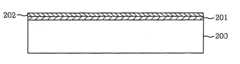
먼저, 도 1을 참조하면, 실리콘기판(200)에 패드 절연막으로서 패드 산화막(201) 및 패드 질화막(202)을 순차적으로 증착한다.First, referring to FIG. 1, a
여기서, 실리콘기판(100)은 화합물반도체, 에피택셜층 등의 반도체기판이 될 수 있다.Here, the silicon substrate 100 may be a semiconductor substrate such as a compound semiconductor or an epitaxial layer.
그리고, 패드 산화막(201)은 패드 질화막(202)이 기판에 직접 증착될 때 발생되는 스트레스를 방지하기 위한 버퍼층으로서, 원치 않을 경우 패드 산화막의 생략이 가능하다.In addition, the
패드 질화막(202)은 후속 화학기계연마시에 연마 정지층으로서 작용하는 바, 연마정지용으로 질화막 이외에 산화 질화막 등의 절연막 사용이 가능하다.Since the
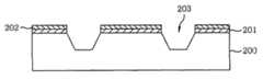
이어서, 도 2를 참조하면 소자분리마스크 및 식각 공정을 통해 소자분리영역의 패드 절연막을 오픈시키고 트렌치(203)를 형성한다.Next, referring to FIG. 2, the pad insulating layer of the device isolation region is opened through the device isolation mask and the etching process to form the
이어서, 도 3에 도시된 바와 같이 질소 이온주입을 실시하여 트렌치 하부의 실리콘기판에 질소 이온주입 영역(204)을 형성한다.Next, as illustrated in FIG. 3, nitrogen ion implantation is performed to form the nitrogen
질소 이온주입시 패드 질화막(202)과 산화막(201)이 마스킹 기능을 하여 오픈된 트렌치 바닥의 실리콘기판에만 선택적 이온주입이 되도록 한다. 이를 위해서는 패드 질화막이 연마 정지층의 기능 이외에 이온주입 마스크로서 충분한 역할을 하도록 그 두께를 조절한다. 그 두께는 소자의 테크놀러지에 따라 달라질 것이다.During the nitrogen ion implantation, the
이어서, 도 4는 열 산화(thermal oxidation)에 의해 라이너 산화막(205)을 형성하고, 이때의 열 공정에 의해 질소 이온주입영역(204)은 실리콘 질화막(206)이 된다. 4, the
실리콘 질화막(206)은 STI 하부의 기판을 통해서 인접한 소자들 간의 상호 도펀트들이 확산되는 것을 방지하는 배리어층 기능을 한다.The
도면에 도시하지는 않았지만 이후, 트렌치(203)를 갭필(gap-fill)하는 소자분리 절연막, 예컨대 산화막을 증착하고, 패드 질화막(202) 표면이 노출되도록 소자분리 절연막을 화학기계연마(CMP)한 다음, 패드 질화막(202)을 제거한다. 이에 의해 STI의 형성이 완료된다.Although not shown in the drawings, a device isolation insulating film, such as an oxide film, is then deposited to gap-fill the
본 발명의 기술 사상은 상기 바람직한 실시 예에 따라 구체적으로 기술되었으나, 상기한 실시 예는 그 설명을 위한 것이며 그 제한을 위한 것이 아님을 주의하여야 한다. 또한, 본 발명의 기술 분야의 통상의 전문가라면 본 발명의 기술 사상의 범위 내에서 다양한 실시 예가 가능함을 이해할 수 있을 것이다.Although the technical spirit of the present invention has been described in detail according to the above preferred embodiment, it should be noted that the above embodiment is for the purpose of description and not of limitation. In addition, those skilled in the art will understand that various embodiments are possible within the scope of the technical idea of the present invention.
본 발명은 고집적화 소자 제조시 STI 하부에 배리어를 형성함으로써, STI 하 부의 기판을 통해서 인접한 소자들 간의 상호 도펀트 확산을 방지하여 준다.The present invention prevents the diffusion of dopants between adjacent devices through the substrate under the STI by forming a barrier under the STI when fabricating a highly integrated device.
또한, 본 발명은 배리어막을 질소 이온주입 공정만을 추가되어 형성할 수 있는 일련의 제조 공정을 제공함으로써, 단순화된 공정으로 소자의 특성 및 제조 수율을 향상시키는 효과가 있다.In addition, the present invention provides a series of manufacturing processes that can form the barrier film by adding only the nitrogen ion implantation process, thereby improving the characteristics and manufacturing yield of the device in a simplified process.
Claims (7)
Translated fromKoreanPriority Applications (1)
| Application Number | Priority Date | Filing Date | Title |
|---|---|---|---|
| KR1020030101155AKR100567878B1 (en) | 2003-12-31 | 2003-12-31 | Trench isolation film formation method of semiconductor device |
Applications Claiming Priority (1)
| Application Number | Priority Date | Filing Date | Title |
|---|---|---|---|
| KR1020030101155AKR100567878B1 (en) | 2003-12-31 | 2003-12-31 | Trench isolation film formation method of semiconductor device |
Publications (2)
| Publication Number | Publication Date |
|---|---|
| KR20050069200A KR20050069200A (en) | 2005-07-05 |
| KR100567878B1true KR100567878B1 (en) | 2006-04-04 |
Family
ID=37259634
Family Applications (1)
| Application Number | Title | Priority Date | Filing Date |
|---|---|---|---|
| KR1020030101155AExpired - Fee RelatedKR100567878B1 (en) | 2003-12-31 | 2003-12-31 | Trench isolation film formation method of semiconductor device |
Country Status (1)
| Country | Link |
|---|---|
| KR (1) | KR100567878B1 (en) |
Cited By (2)
| Publication number | Priority date | Publication date | Assignee | Title |
|---|---|---|---|---|
| US9196729B2 (en) | 2013-07-17 | 2015-11-24 | Samsung Electronics Co., Ltd. | Semiconductor device having buried channel array and method of manufacturing the same |
| US9490160B2 (en) | 2013-03-04 | 2016-11-08 | Samsung Electronics Co., Ltd. | Method of manufacturing semiconductor device |
Families Citing this family (1)
| Publication number | Priority date | Publication date | Assignee | Title |
|---|---|---|---|---|
| KR100831260B1 (en) | 2006-12-29 | 2008-05-22 | 동부일렉트로닉스 주식회사 | How to Form Corner Roundings in Trench Isolators |
- 2003
- 2003-12-31KRKR1020030101155Apatent/KR100567878B1/ennot_activeExpired - Fee Related
Cited By (2)
| Publication number | Priority date | Publication date | Assignee | Title |
|---|---|---|---|---|
| US9490160B2 (en) | 2013-03-04 | 2016-11-08 | Samsung Electronics Co., Ltd. | Method of manufacturing semiconductor device |
| US9196729B2 (en) | 2013-07-17 | 2015-11-24 | Samsung Electronics Co., Ltd. | Semiconductor device having buried channel array and method of manufacturing the same |
Also Published As
| Publication number | Publication date |
|---|---|
| KR20050069200A (en) | 2005-07-05 |
Similar Documents
| Publication | Publication Date | Title |
|---|---|---|
| EP1213757B1 (en) | Integrated circuits having adjacent p-type doped regions having shallow trench isolation structures without liner layers therebetween and methods of forming same | |
| US5308786A (en) | Trench isolation for both large and small areas by means of silicon nodules after metal etching | |
| US6277709B1 (en) | Method of forming shallow trench isolation structure | |
| US5294562A (en) | Trench isolation with global planarization using flood exposure | |
| JPH09321132A (en) | Method for separating trench element in semiconductor device | |
| US20020127818A1 (en) | Recess-free trench isolation structure and method of forming the same | |
| US6544861B2 (en) | Method for forming isolation trench | |
| KR100379336B1 (en) | Fabrication method of isolation region for semiconductor devices | |
| KR100567878B1 (en) | Trench isolation film formation method of semiconductor device | |
| US6344374B1 (en) | Method of fabricating insulators for isolating electronic devices | |
| KR100596876B1 (en) | Device Separator Formation Method of Semiconductor Device | |
| KR100365740B1 (en) | method of trench isolation using nitrogen diffusion | |
| KR100546722B1 (en) | Semiconductor device manufacturing method | |
| KR100672769B1 (en) | Device isolation film formation method of semiconductor device | |
| KR100567877B1 (en) | Device Separating Method of Semiconductor Device | |
| KR20030001941A (en) | Method For Manufacturing Semiconductor Devices | |
| KR100419754B1 (en) | A method for forming a field oxide of a semiconductor device | |
| KR20090063657A (en) | Device Separator Formation Method | |
| KR100455726B1 (en) | Method for forming isolation layer in semiconductor device | |
| KR20030088235A (en) | Method for forming isolation layer of semiconductor device | |
| KR19990048786A (en) | Method of forming device isolation film of semiconductor device | |
| KR20000043906A (en) | Method for manufacturing semiconductor device | |
| KR100209927B1 (en) | Method for isolating semiconductor device | |
| KR100430582B1 (en) | Method for manufacturing semiconductor device | |
| KR100274349B1 (en) | Method of forming a field oxide firm in a semiconductor device |
Legal Events
| Date | Code | Title | Description |
|---|---|---|---|
| A201 | Request for examination | ||
| PA0109 | Patent application | St.27 status event code:A-0-1-A10-A12-nap-PA0109 | |
| PA0201 | Request for examination | St.27 status event code:A-1-2-D10-D11-exm-PA0201 | |
| R18-X000 | Changes to party contact information recorded | St.27 status event code:A-3-3-R10-R18-oth-X000 | |
| PG1501 | Laying open of application | St.27 status event code:A-1-1-Q10-Q12-nap-PG1501 | |
| D13-X000 | Search requested | St.27 status event code:A-1-2-D10-D13-srh-X000 | |
| D14-X000 | Search report completed | St.27 status event code:A-1-2-D10-D14-srh-X000 | |
| E902 | Notification of reason for refusal | ||
| PE0902 | Notice of grounds for rejection | St.27 status event code:A-1-2-D10-D21-exm-PE0902 | |
| E13-X000 | Pre-grant limitation requested | St.27 status event code:A-2-3-E10-E13-lim-X000 | |
| P11-X000 | Amendment of application requested | St.27 status event code:A-2-2-P10-P11-nap-X000 | |
| P13-X000 | Application amended | St.27 status event code:A-2-2-P10-P13-nap-X000 | |
| E701 | Decision to grant or registration of patent right | ||
| PE0701 | Decision of registration | St.27 status event code:A-1-2-D10-D22-exm-PE0701 | |
| PR1002 | Payment of registration fee | St.27 status event code:A-2-2-U10-U11-oth-PR1002 Fee payment year number:1 | |
| GRNT | Written decision to grant | ||
| PR0701 | Registration of establishment | St.27 status event code:A-2-4-F10-F11-exm-PR0701 | |
| PG1601 | Publication of registration | St.27 status event code:A-4-4-Q10-Q13-nap-PG1601 | |
| PN2301 | Change of applicant | St.27 status event code:A-5-5-R10-R13-asn-PN2301 St.27 status event code:A-5-5-R10-R11-asn-PN2301 | |
| PN2301 | Change of applicant | St.27 status event code:A-5-5-R10-R13-asn-PN2301 St.27 status event code:A-5-5-R10-R11-asn-PN2301 | |
| PR1001 | Payment of annual fee | St.27 status event code:A-4-4-U10-U11-oth-PR1001 Fee payment year number:4 | |
| PR1001 | Payment of annual fee | St.27 status event code:A-4-4-U10-U11-oth-PR1001 Fee payment year number:5 | |
| PR1001 | Payment of annual fee | St.27 status event code:A-4-4-U10-U11-oth-PR1001 Fee payment year number:6 | |
| FPAY | Annual fee payment | Payment date:20120221 Year of fee payment:7 | |
| PR1001 | Payment of annual fee | St.27 status event code:A-4-4-U10-U11-oth-PR1001 Fee payment year number:7 | |
| LAPS | Lapse due to unpaid annual fee | ||
| PC1903 | Unpaid annual fee | St.27 status event code:A-4-4-U10-U13-oth-PC1903 Not in force date:20130330 Payment event data comment text:Termination Category : DEFAULT_OF_REGISTRATION_FEE | |
| PC1903 | Unpaid annual fee | St.27 status event code:N-4-6-H10-H13-oth-PC1903 Ip right cessation event data comment text:Termination Category : DEFAULT_OF_REGISTRATION_FEE Not in force date:20130330 | |
| P22-X000 | Classification modified | St.27 status event code:A-4-4-P10-P22-nap-X000 |