KR100563818B1 - Fixture for baffle plate of plasma etching chamber - Google Patents
Fixture for baffle plate of plasma etching chamberDownload PDFInfo
- Publication number
- KR100563818B1 KR100563818B1KR1020030053475AKR20030053475AKR100563818B1KR 100563818 B1KR100563818 B1KR 100563818B1KR 1020030053475 AKR1020030053475 AKR 1020030053475AKR 20030053475 AKR20030053475 AKR 20030053475AKR 100563818 B1KR100563818 B1KR 100563818B1
- Authority
- KR
- South Korea
- Prior art keywords
- baffle plate
- holes
- baffle
- etching chamber
- jig
- Prior art date
- Legal status (The legal status is an assumption and is not a legal conclusion. Google has not performed a legal analysis and makes no representation as to the accuracy of the status listed.)
- Expired - Fee Related
Links
Images


Classifications
- H—ELECTRICITY
- H01—ELECTRIC ELEMENTS
- H01J—ELECTRIC DISCHARGE TUBES OR DISCHARGE LAMPS
- H01J37/00—Discharge tubes with provision for introducing objects or material to be exposed to the discharge, e.g. for the purpose of examination or processing thereof
- H01J37/32—Gas-filled discharge tubes
- H01J37/32431—Constructional details of the reactor
- H01J37/32623—Mechanical discharge control means
- H01J37/32633—Baffles
- H—ELECTRICITY
- H01—ELECTRIC ELEMENTS
- H01L—SEMICONDUCTOR DEVICES NOT COVERED BY CLASS H10
- H01L21/00—Processes or apparatus adapted for the manufacture or treatment of semiconductor or solid state devices or of parts thereof
- H01L21/67—Apparatus specially adapted for handling semiconductor or electric solid state devices during manufacture or treatment thereof; Apparatus specially adapted for handling wafers during manufacture or treatment of semiconductor or electric solid state devices or components ; Apparatus not specifically provided for elsewhere
- H01L21/67005—Apparatus not specifically provided for elsewhere
- H01L21/67011—Apparatus for manufacture or treatment
- H01L21/67017—Apparatus for fluid treatment
- H01L21/67063—Apparatus for fluid treatment for etching
- H01L21/67069—Apparatus for fluid treatment for etching for drying etching
Landscapes
- Engineering & Computer Science (AREA)
- Physics & Mathematics (AREA)
- Condensed Matter Physics & Semiconductors (AREA)
- General Physics & Mathematics (AREA)
- Manufacturing & Machinery (AREA)
- Computer Hardware Design (AREA)
- Microelectronics & Electronic Packaging (AREA)
- Power Engineering (AREA)
- Plasma & Fusion (AREA)
- Chemical & Material Sciences (AREA)
- Analytical Chemistry (AREA)
- Drying Of Semiconductors (AREA)
Abstract
Translated fromKoreanDescription
Translated fromKorean도 1은 종래 기술에 의한 플라즈마 에칭 장치를 나타낸 개략 구성도.1 is a schematic configuration diagram showing a plasma etching apparatus according to the prior art.
도 2는 도 1의 배플 플레이트를 나타낸 평면도.2 is a plan view of the baffle plate of FIG.
도 3은 본 발명에 의한 플라즈마 에칭 챔버의 배플 플레이트를 위한 치구를 나타낸 분해 사시도.Figure 3 is an exploded perspective view showing the jig for the baffle plate of the plasma etching chamber according to the present invention.
도 4는 도 3의 치구의 배플 홀의 오버랩을 나타낸 요부 평면도.4 is a plan view of the main portion showing the overlap of the baffle holes of the jig of FIG.
도 5는 도 4의 배플 홀의 오버랩을 나타낸 요부 단면도.5 is a sectional view showing the principal parts of the baffle hole in FIG. 4;
본 발명은 플라즈마 에칭 챔버의 배플 플레이트(baffle plate)에 관한 것으로, 더욱 상세하게는 배플 플레이트의 배플 홀들의 최적 사이즈를 용이하게 결정하도록 한 플라즈마 에칭 챔버의 배플 플레이트를 위한 치구에 관한 것이다.The present invention relates to a baffle plate of a plasma etch chamber, and more particularly to a jig for a baffle plate of a plasma etch chamber to facilitate the determination of the optimal size of the baffle holes of the baffle plate.
일반적으로, 에칭공정은 반도체 소자를 제조하기 위한 공정 중의 하나로서 습식 에칭공정과 건식 에칭공정으로 구분된다. 반도체 소자의 고집적화가 진행됨에 따라 반도체 소자의 미세화되므로 반도체 소자의 미세한 패턴을 형성하는데 상기 건식 에칭공정이 주로 사용되고 있는 실정이다. 상기 건식 에칭공정의 대표적인 공정이 플라즈마를 이용한 에칭공정이다. 상기 플라즈마를 이용한 에칭 공정은 전형적으로 평행판 타입의 에칭장치에서 수행된다.In general, an etching process is one of processes for manufacturing a semiconductor device, and is classified into a wet etching process and a dry etching process. As the integration of semiconductor devices increases, the semiconductor devices become finer, and thus, the dry etching process is mainly used to form fine patterns of semiconductor devices. A typical process of the dry etching process is an etching process using plasma. The etching process using the plasma is typically performed in a parallel plate type etching apparatus.
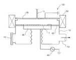
상기 평행판 타입의 일반적인 에칭장치는 도 1에 도시된 바와 같이, 에칭 반응을 위한 내부 공간을 확보하는 에칭 챔버(100)를 포함한다. 상기 에칭 챔버(100)는 대략 실린더 형상의 본체(10)를 가진다. 상기 본체(10)의 상면 내벽에 상부 전극(20)이 설치되고, 상기 본체(10)의 저면 내벽에 하부 전극(30)이 설치된다. 상기 하부 전극(30)은 에칭할 웨이퍼(1)를 지지하기 위한 지지대로서 역할을 한다. 고주파(RF) 전원 공급부(40)가 고주파 전원을 상기 하부 전극(30)에 공급하고, 상기 상부 전극(20)이 접지된다. 이때, 전장(E)이 상기 상부 전극(20)과 하부 전극(30) 사이에 생성된다. 자장 생성부(50)가 상기 본체(110)의 측면 외벽에 설치되어 자장(B)을 생성시킨다. 공정 가스 공급부(미도시)가 상기 본체(10)의 가스 공급라인(11)을 거쳐 공정 가스를 상기 본체(10)의 내부 공간으로 공급한다. 펌핑부(미도시)가 상기 본체(10)의 가스 배기구(13)를 거쳐 상기 본체(10)의 내부 공간을 펌핑한다. 상기 웨이퍼(1)의 반송을 위한 개폐용 도아(15)가 상기 본체(10)의 측벽에 설치되고, 상기 하부 전극(30)이 승강기(미도시)에 의해 수직으로 승강한다.The general etching apparatus of the parallel plate type includes an
또한, 배플 플레이트(baffle plate)(60)가 상기 하부 전극(30)과 상기 본체(10)의 측면 내벽 사이에 설치됨으로써 상기 본체(10)의 내부 공간을 상, 하측 내부 공간(12),(14)으로 각각 구분한다. 상기 상측 내부 공간(12)은 에칭 공정을 위한 공간이고, 상기 하측 내부 공간(14)은 상기 웨이퍼(1)의 반송을 위한 공간이다.In addition, a
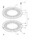
또한, 상기 배플 플레이트(60)가 도 2에 도시된 바와 같이, 원판 링 형상의 본체(61)를 가지며, 대략 사각 형상의 배플 홀들(63)이 상기 본체(61)에 형성된다. 상기 배플 홀들(63)이 상기 본체(61)의 방사상 방향(R)과 동일한 방향으로 직선 연장하여 형성되고, 상기 본체(61)의 원주 방향으로 일정 간격을 두고 이격하여 배치된다.In addition, as shown in FIG. 2, the
여기서, 상기 배플 플레이트(60)의 배플 홀들(63)의 총 면적은 상기 배플 플레이트(60)의 직경 및 면적과, 에칭공정의 조건, 예를 들어 공정 가스의 종류 및 유량, 챔버 내의 압력 등을 고려하여 상기 가스 배기구(13)의 면적 대비 일정 비율로 결정된다. 이는 상측 내부 공간(12)의 압력 변화를 감소시키고 미반응 가스 및 반응 부산물의 폴리머 등을 원활히 배기시키기 위함이다.In this case, the total area of the
그러데, 종래에는 에칭 챔버용 배플 플레이트의 배플 홀들의 총 면적을 최적의 값으로 결정하기 위해 에칭 챔버에 배플 플레이트를 적용한 상태에서 에칭공정을 실제로 진행한 후 상기 에칭공정의 특성을 분석한다. 이때, 상기 에칭공정의 특성이 당초 원하는 특성과 상이할 경우, 상기 배플 플레이트의 배플 홀들의 총 면적을 변경시키기 위해 새로운 배플 플레이트를 제작한다. 그런 다음, 상기 새로운 배플 플레이트를 상기 에칭 챔버에 다시 적용시킨 상태에서 상기 에칭공정을 진행시킨 후 에칭공정의 특성을 분석한다. 이때에도, 상기 에칭공정의 특성이 당초 원하 는 특성과 상이할 경우, 또다시 새로운 배플 플레이트를 제작한다.However, conventionally, in order to determine the total area of the baffle holes of the baffle plate for the etching chamber as an optimal value, the etching process is actually performed in the state where the baffle plate is applied to the etching chamber, and then the characteristics of the etching process are analyzed. In this case, when the characteristics of the etching process is different from the original desired characteristics, a new baffle plate is manufactured to change the total area of the baffle holes of the baffle plate. Then, the etching process is performed while the new baffle plate is applied to the etching chamber again, and then the characteristics of the etching process are analyzed. In this case, when the characteristics of the etching process are different from those originally desired, a new baffle plate is manufactured again.
그러나, 종래에는 배플 플레이트의 배플 홀들의 최적 총면적을 결정하기 위해 여러번의 시행착오를 거치면서 여러장의 배플 플레이트를 제작하여 왔다. 이는 에칭공정 조건에 배플 플레이트의 배플 홀들의 총면적을 최적화시키는데 많은 어려움이 있다.However, conventionally, several baffle plates have been manufactured through several trials and errors in order to determine an optimal total area of the baffle holes of the baffle plate. This has many difficulties in optimizing the total area of the baffle holes of the baffle plate to the etching process conditions.
또한, 상기 시행착오를 거칠 때마다 새로운 배플 플레이트를 제작하여야 하므로 상기 에칭 챔버에 실제로 적용할 배플 플레이트를 선정하는데 많은 비용과 시간이 소요되는 문제점이 있다.In addition, since a new baffle plate has to be manufactured every time the trial and error, there is a problem in that it takes a lot of cost and time to select a baffle plate to be actually applied to the etching chamber.
따라서, 본 발명은 에칭장치의 에칭공정 조건의 변화에 따른 배플 플레이트를 용이하게 최적화시키는데 있다.Accordingly, the present invention is to easily optimize the baffle plate according to the change of the etching process conditions of the etching apparatus.
본 발명의 다른 목적은 최적의 배플 플레이트를 선정하는데 소요되는 비용과 시간을 줄이는데 있다.
Another object of the present invention is to reduce the cost and time required to select the optimal baffle plate.
이와 같은 목적을 달성하기 위한 본 발명에 의한 플라즈마 에칭 챔버의 배플 플레이트를 위한 치구는The jig for the baffle plate of the plasma etching chamber according to the present invention for achieving the above object is
에칭 챔버의 측면 내벽과 하부 전극 사이에 설치될 배플 플레이트 형상과 동일한 형상으로 이루어지며, 상기 배플 플레이트의 배플 홀들과 동일하게 관통홀들 이 형성된 상부 본체; 상기 상부 본체와 동일한 형상으로 이루어지며, 상기 배플 플레이트의 배플 홀들과 동일하게 관통 홀들이 형성된 하부 본체; 및 상기 상부 본체와 상기 하부 본체를 체결하며, 상기 상부 본체와 상기 하부 본체의 서로 대응하는 관통 홀들의 수직 오버랩 면적을 조절하는 체결 수단을 포함하는 것을 특징으로 한다.An upper body having the same shape as the baffle plate to be installed between the side inner wall of the etching chamber and the lower electrode, and having through holes formed in the same manner as the baffle holes of the baffle plate; A lower body having the same shape as the upper body and having through holes formed in the same manner as the baffle holes of the baffle plate; And fastening means for fastening the upper main body and the lower main body and adjusting vertical overlap areas of the through holes corresponding to each other of the upper main body and the lower main body.
바람직하게는, 상기 체결 수단은 나사를 이용할 수 있다.Preferably, the fastening means may use a screw.
바람직하게는, 상기 상부 본체와 상기 하부 본체의 대응하는 부분에 상기 나사의 삽입을 위한 관통 홀이 각각 형성되고, 상기 하부 본체의 관통홀이 상기 수직 오버랩 면적의 조절을 위해 상기 하부 본체의 원주 방향으로 소정의 길이만큼 연장하여 형성될 수 있다.Preferably, through holes for insertion of the screw are respectively formed in corresponding portions of the upper body and the lower body, and the through holes of the lower body are arranged in the circumferential direction of the lower body to adjust the vertical overlap area. It may be formed to extend by a predetermined length.
이하, 본 발명에 의한 플라즈마 에칭 챔버의 배플 플레이트를 위한 치구를 첨부된 도면을 참조하여 상세히 설명하기로 한다.Hereinafter, a jig for a baffle plate of a plasma etching chamber according to the present invention will be described in detail with reference to the accompanying drawings.
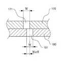
도 3을 참조하면, 본 발명의 배플 플레이트를 위한 치구(160)는 상, 하부 본체(170),(180)를 포함한다. 상기 상, 하부 본체(170),(180)가 임의의 체결 수단, 예를 들어 나사(191) 및 너트(193)에 의해 체결된다.Referring to FIG. 3, the
상기 상부 본체(170)가 도 1의 본체(10)의 측면 내벽과 하부 전극(30) 사이에 배치될 수 있도록 배플 플레이트(60)와 동일한 직경을 갖는 원판 링 형상으로 이루어진다. The
상기 상부 본체(170)에는 배플 홀들(171)이 도 2의 배플 플레이트(60)의 배 플 홀들(63)과 동일한 형상으로 형성된다. 즉, 상기 배플 홀들(171)과 상기 배플 홀들(63)의 사이즈, 개수 및 위치가 동일하다. 상기 본체(170)의 중앙부에는 상기 하부 전극(30)을 삽입하여 면접할 수 있도록 원형 중공홀(173)이 형성된다.
상기 하부 본체(180)에는 배플 홀들(181)이 도 2의 배플 플레이트(60)의 배플 홀들(63)과 동일하게 형성된다. 즉, 상기 배플 홀들(181)과 상기 배플 홀들(63)의 사이즈, 개수 및 위치가 동일하다. 상기 본체(180)의 중앙부에는 상기 하부 전극(30)을 삽입하여 면접할 수 있도록 원형 중공홀(193)이 형성된다.
또한, 상기 상부 본체(170)의 가장자리부에 관통홀(175)이 형성되고, 상기 하부 본체(180)의 가장자리부에는 상기 관통홀(175)과 동일 수직선 상에 위치하도록 관통홀(185)이 형성된다. 상기 관통홀(175)은 나사(177)를 삽입하기에 적합한 직경을 갖는 원형 형상의 홀이다. 상기 관통홀(185)은 상기 나사(177)를 삽입하기에 적합한 폭을 가지며 원주 방향을 따라 곡선으로 임의의 길이(D)로 길게 연장된, 대략 사각 형상의 홀이다. 상기 관통홀(185)의 길이(L)는 상기 상, 하부 본체(170),(180)을 서로 반대의 원주 방향으로 길이(L)만큼 회전시킬 수 있도록 상기 나사(177)의 직경보다 크게 설정되는데, 이는 도 4 및 도 5에 도시된 바와 같이, 상기 상, 하부 본체(170),(180)의 배플 홀(171),(181)을 수직으로 오버랩하는 실질적인 폭(Weff)을 조절하기 위함이다. 상기 배플 홀(171),(181)의 폭이 W이고, 상기 배플 홀(171),(181)의 길이가 L이다.In addition, a
이와 같이 상, 하부 본체(170),(180)를 나사 체결한 치구(160)를 도 1의 에칭 챔버(100)의 배플 플레이트(60)의 대신에 상기 에칭 챔버(100)에 설치한 상태에 서 에칭 공정을 실제로 진행한 후 상기 에칭공정의 특성을 분석한다.Thus, in the state where the
이때, 상기 에칭공정 특성이 당초 원하는 특성과 상이할 경우, 상기 치구(160)를 상기 에칭 챔버(100)로부터 외부로 이동시킨 후 상기 치구(160)의 상, 하부 본체(170),(180)를 나사 체결한 나사(191)와 너트(193)를 분리시킨다. 그런 다음, 상기 상, 하부 본체(170),(180)를 서로 반대의 원주 방향으로 회전시킴으로써 새로운 원하는 값의 폭(Weff)을 조절시킨다.In this case, when the etching process characteristics are different from the original desired characteristics, after moving the
상기 조절된 폭(Weff)을 그대로 유지시키기 위해 상기 상, 하부 본체(170),(180)를 나사(191)와 너트(193)에 의해 나사 체결시킨다. 이후, 상기 치구(160)를 에칭 챔버(100)에 다시 설치한 상태에서 상기 에칭 공정을 동일하게 진행하고 나서 상기 에칭공정의 특성을 분석한다.In order to maintain the adjusted width Weff, the upper and lower
이러한 절차를 반복 진행하면, 상기 폭(Weff)을 상기 에칭 공정에 적합한 최적의 값으로 결정할 수 있다. 그 결과, 상기 폭(Weff)의 최적 값과, 상기 관통홀(171),(181)의 길이 및 개수를 곱셈으로 연산한 값을 상기 에칭 챔버(100)에 적용될 배플 플레이트의 배플 홀들의 총면적을 최적의 값으로 결정할 수 있다.By repeating this procedure, the width Weff can be determined to be an optimal value suitable for the etching process. As a result, the total area of the baffle holes of the baffle plate to be applied to the
따라서, 본 발명은 치구를 이용하여 에칭 챔버에 적용할 배플 플레이트의 배플 홀들의 최적의 총 면적을 용이하게 결정할 수 있다. 그러므로, 상기 배플 홀들의 최적의 총 면적을 결정하기 위한 여러번의 배플 플레이트 제작을 방지할 수 있고, 나아가 상기 에칭 챔버에 실제 적용할 배플 플레이트의 제작에 소요되는 비용과 시간이 줄어든다.Accordingly, the present invention can easily determine the optimal total area of the baffle holes of the baffle plate to be applied to the etching chamber using the jig. Therefore, it is possible to prevent the production of a number of baffle plates to determine the optimal total area of the baffle holes, further reducing the cost and time required to manufacture the baffle plate to be actually applied to the etching chamber.
한편, 설명의 편의상 상기 상, 하부 본체의 체결 수단으로서 나사를 이용하 였지만, 이외에도 사용 가능한 다양한 형태의 체결 수단을 적용할 수 있음은 자명한 사실이다. 또한, 배플 플레이트의 배플 홀들이 방사상 방향으로 연장하여 형성된 것을 기준으로 설명하였으나, 상기 배플 홀들이 상기 방사상 방향과 임의의 경사 각도로 기울어져 형성된 경우에도 본 발명을 동일하게 실시할 수 있다.On the other hand, for convenience of description, although the screw was used as the fastening means of the upper and lower bodies, it is apparent that various other fastening means that can be used can be applied. In addition, the baffle holes of the baffle plate have been described on the basis of extending in the radial direction, but the present invention can be implemented in the same manner even when the baffle holes are formed to be inclined at an inclined angle with respect to the radial direction.
이상에서 설명한 바와 같이, 본 발명에 의한 플라즈마 에칭 챔버의 배플 플레이트를 위한 치구는 에칭 챔버의 측면 내벽과 하부 전극 사이에 설치될 수 있도록 배플 플레이트와 동일한 원판 링 형상의 상, 하부 본체를 갖는다. 상기 상, 하부 본체에는 배플 플레이트의 배플 홀들과 동일한 형태로 관통 홀들이 형성된다. 상기 상, 하 본체의 가장자리에는 상기 상, 하부 본체를 나사에 의해 체결된다. 상기 나사의 삽입을 위한 상기 하부 본체의 관통 홀에는 상, 하부 본체의 관통 홀의 오버랩 면적을 조절하기 위해 상기 나사의 직경보다 큰 길이를 갖는다.As described above, the jig for the baffle plate of the plasma etching chamber according to the present invention has an upper and lower body having the same disc ring shape as the baffle plate so that it can be installed between the side inner wall of the etching chamber and the lower electrode. Through-holes are formed in the upper and lower bodies in the same form as the baffle holes of the baffle plate. The upper and lower bodies are fastened to the edges of the upper and lower bodies by screws. The through hole of the lower body for the insertion of the screw has a length greater than the diameter of the screw to adjust the overlap area of the through hole of the upper, lower body.
따라서, 본 발명은 상기 치구를 에칭 챔버에 적용한 후 에칭 공정을 진행하고 그 결과에 따라 상기 치구의 상, 하부 본체의 관통홀들의 수직으로 오버랩하는 폭을 용이하게 조절할 수 있다.Therefore, the present invention can easily adjust the width of the vertical overlap of the through holes of the upper and lower body of the jig after applying the jig to the etching chamber and proceeding the etching process.
따라서, 본 발명은 배플 플레이트의 배플 홀들의 최적 총 면적을 구하기 위해 여러번의 배플 플레이트 제작을 방지할 수 있고, 나아가, 상기 에칭 챔버에 실제로 적용할 배플 플레이트의 제작에 소요되는 비용과 시간을 줄일 수가 있다.Accordingly, the present invention can prevent the production of multiple baffle plates in order to obtain the optimal total area of the baffle holes of the baffle plate, and furthermore, the cost and time required to manufacture the baffle plate actually applied to the etching chamber can be reduced. have.
한편, 본 발명은 도시된 도면과 상세한 설명에 기술된 내용에 한정하지 않으 며 본 발명의 사상을 벗어나지 않는 범위 내에서 다양한 형태의 변형도 가능함은 이 분야에 통상의 지식을 가진 자에게는 자명한 사실이다.Meanwhile, the present invention is not limited to the contents described in the drawings and the detailed description, and various modifications may be made without departing from the spirit of the present invention, which is obvious to those skilled in the art. to be.
Claims (3)
Translated fromKoreanPriority Applications (1)
| Application Number | Priority Date | Filing Date | Title |
|---|---|---|---|
| KR1020030053475AKR100563818B1 (en) | 2003-08-01 | 2003-08-01 | Fixture for baffle plate of plasma etching chamber |
Applications Claiming Priority (1)
| Application Number | Priority Date | Filing Date | Title |
|---|---|---|---|
| KR1020030053475AKR100563818B1 (en) | 2003-08-01 | 2003-08-01 | Fixture for baffle plate of plasma etching chamber |
Publications (2)
| Publication Number | Publication Date |
|---|---|
| KR20050015019A KR20050015019A (en) | 2005-02-21 |
| KR100563818B1true KR100563818B1 (en) | 2006-03-28 |
Family
ID=37225861
Family Applications (1)
| Application Number | Title | Priority Date | Filing Date |
|---|---|---|---|
| KR1020030053475AExpired - Fee RelatedKR100563818B1 (en) | 2003-08-01 | 2003-08-01 | Fixture for baffle plate of plasma etching chamber |
Country Status (1)
| Country | Link |
|---|---|
| KR (1) | KR100563818B1 (en) |
Families Citing this family (8)
| Publication number | Priority date | Publication date | Assignee | Title |
|---|---|---|---|---|
| KR100734779B1 (en)* | 2005-10-05 | 2007-07-03 | 세메스 주식회사 | Focus ring of semiconductor manufacturing device |
| KR100694799B1 (en)* | 2006-04-20 | 2007-03-14 | 세메스 주식회사 | Semiconductor Ashing Device |
| KR101410819B1 (en)* | 2007-07-10 | 2014-06-24 | 주성엔지니어링(주) | Substrate processing apparatus comprising tunable baffle and exhaustion method using the same |
| KR101091309B1 (en)* | 2009-08-18 | 2011-12-07 | 주식회사 디엠에스 | Plasma Etching Equipment |
| KR101131898B1 (en)* | 2010-09-03 | 2012-04-03 | 우범제 | Lid Assembly of plasma etching apparatus |
| KR20130085147A (en)* | 2012-01-19 | 2013-07-29 | 서울옵토디바이스주식회사 | Fabricating apparatus of semiconductor device |
| KR20180014900A (en)* | 2016-08-01 | 2018-02-12 | 세메스 주식회사 | Apparatus for treating substrate |
| CN109826978B (en)* | 2019-02-28 | 2024-08-02 | 常州那央生物科技有限公司 | Micro-pore flow channel construction method for micro-reaction, micro-reaction assembly and working method thereof |
Citations (4)
| Publication number | Priority date | Publication date | Assignee | Title |
|---|---|---|---|---|
| KR20010041677A (en)* | 1998-03-06 | 2001-05-25 | 히가시 데쓰로 | Processing apparatus |
| US6245192B1 (en)* | 1999-06-30 | 2001-06-12 | Lam Research Corporation | Gas distribution apparatus for semiconductor processing |
| JP2001179078A (en)* | 1999-12-24 | 2001-07-03 | Tokyo Electron Ltd | Baffle plate, apparatus and method for manufacturing the same, and gas processing apparatus including baffle plate |
| KR20050004332A (en)* | 2003-07-02 | 2005-01-12 | 주성엔지니어링(주) | Device of baffle which make possible adjusting elevation |
- 2003
- 2003-08-01KRKR1020030053475Apatent/KR100563818B1/ennot_activeExpired - Fee Related
Patent Citations (4)
| Publication number | Priority date | Publication date | Assignee | Title |
|---|---|---|---|---|
| KR20010041677A (en)* | 1998-03-06 | 2001-05-25 | 히가시 데쓰로 | Processing apparatus |
| US6245192B1 (en)* | 1999-06-30 | 2001-06-12 | Lam Research Corporation | Gas distribution apparatus for semiconductor processing |
| JP2001179078A (en)* | 1999-12-24 | 2001-07-03 | Tokyo Electron Ltd | Baffle plate, apparatus and method for manufacturing the same, and gas processing apparatus including baffle plate |
| KR20050004332A (en)* | 2003-07-02 | 2005-01-12 | 주성엔지니어링(주) | Device of baffle which make possible adjusting elevation |
Also Published As
| Publication number | Publication date |
|---|---|
| KR20050015019A (en) | 2005-02-21 |
Similar Documents
| Publication | Publication Date | Title |
|---|---|---|
| KR102779387B1 (en) | Low volume showerhead with faceplate holes for improved flow uniformity | |
| KR102451669B1 (en) | Upper electrode having varying thickness for plasma processing | |
| JP5294626B2 (en) | Apparatus for controlling gas flow in a semiconductor substrate processing chamber | |
| JP4565743B2 (en) | Semiconductor processing chamber electrode and method of manufacturing the same | |
| CN206225317U (en) | For the device and plasma process chamber of corona treatment | |
| KR102424818B1 (en) | Plasma processing apparatus and focus ring | |
| US7416635B2 (en) | Gas supply member and plasma processing apparatus | |
| US7829815B2 (en) | Adjustable electrodes and coils for plasma density distribution control | |
| US20170236743A1 (en) | Wafer lift ring system for wafer transfer | |
| JP5589840B2 (en) | Integrated steerability array placement to minimize non-uniformity | |
| US20060060303A1 (en) | Plasma processing system and method | |
| KR20030009909A (en) | Dry Etching Apparatus for Manufacturing Semiconductor Devices | |
| JP3224900U (en) | Apparatus for reducing polymer deposition | |
| JP7296456B2 (en) | Process chamber with improved edge processing of substrates | |
| KR100563818B1 (en) | Fixture for baffle plate of plasma etching chamber | |
| JP2010529656A (en) | Apparatus and method for improving processing uniformity of plasma process | |
| KR20200051505A (en) | Placing table and substrate processing apparatus | |
| KR102667942B1 (en) | Apparatus for placing an object to be processed and processing apparatus | |
| KR101686564B1 (en) | Locking assembly and Apparatus for treating substrate with the assembly | |
| JP2011176361A (en) | Parallel-plate dry etching apparatus and method of dry etching | |
| KR20050013734A (en) | Plasma Etching Apparatus | |
| KR20190004255A (en) | Apparatus for treating substrate | |
| JPH09283493A (en) | Electrode for plasma etching and plasma etching equipment | |
| KR100510076B1 (en) | Plasma Etching Apparatus | |
| JP2000208490A (en) | Surface treatment device |
Legal Events
| Date | Code | Title | Description |
|---|---|---|---|
| A201 | Request for examination | ||
| PA0109 | Patent application | St.27 status event code:A-0-1-A10-A12-nap-PA0109 | |
| PA0201 | Request for examination | St.27 status event code:A-1-2-D10-D11-exm-PA0201 | |
| R17-X000 | Change to representative recorded | St.27 status event code:A-3-3-R10-R17-oth-X000 | |
| R18-X000 | Changes to party contact information recorded | St.27 status event code:A-3-3-R10-R18-oth-X000 | |
| D13-X000 | Search requested | St.27 status event code:A-1-2-D10-D13-srh-X000 | |
| PG1501 | Laying open of application | St.27 status event code:A-1-1-Q10-Q12-nap-PG1501 | |
| D14-X000 | Search report completed | St.27 status event code:A-1-2-D10-D14-srh-X000 | |
| E902 | Notification of reason for refusal | ||
| PE0902 | Notice of grounds for rejection | St.27 status event code:A-1-2-D10-D21-exm-PE0902 | |
| P11-X000 | Amendment of application requested | St.27 status event code:A-2-2-P10-P11-nap-X000 | |
| P13-X000 | Application amended | St.27 status event code:A-2-2-P10-P13-nap-X000 | |
| E701 | Decision to grant or registration of patent right | ||
| PE0701 | Decision of registration | St.27 status event code:A-1-2-D10-D22-exm-PE0701 | |
| GRNT | Written decision to grant | ||
| PR0701 | Registration of establishment | St.27 status event code:A-2-4-F10-F11-exm-PR0701 | |
| PR1002 | Payment of registration fee | St.27 status event code:A-2-2-U10-U11-oth-PR1002 Fee payment year number:1 | |
| PG1601 | Publication of registration | St.27 status event code:A-4-4-Q10-Q13-nap-PG1601 | |
| PN2301 | Change of applicant | St.27 status event code:A-5-5-R10-R13-asn-PN2301 St.27 status event code:A-5-5-R10-R11-asn-PN2301 | |
| PN2301 | Change of applicant | St.27 status event code:A-5-5-R10-R13-asn-PN2301 St.27 status event code:A-5-5-R10-R11-asn-PN2301 | |
| LAPS | Lapse due to unpaid annual fee | ||
| PC1903 | Unpaid annual fee | St.27 status event code:A-4-4-U10-U13-oth-PC1903 Not in force date:20090318 Payment event data comment text:Termination Category : DEFAULT_OF_REGISTRATION_FEE | |
| PC1903 | Unpaid annual fee | St.27 status event code:N-4-6-H10-H13-oth-PC1903 Ip right cessation event data comment text:Termination Category : DEFAULT_OF_REGISTRATION_FEE Not in force date:20090318 | |
| P22-X000 | Classification modified | St.27 status event code:A-4-4-P10-P22-nap-X000 |