KR100562318B1 - Nonvolatile Semiconductor Memory Device and Manufacturing Method Thereof - Google Patents
Nonvolatile Semiconductor Memory Device and Manufacturing Method ThereofDownload PDFInfo
- Publication number
- KR100562318B1 KR100562318B1KR1020030097919AKR20030097919AKR100562318B1KR 100562318 B1KR100562318 B1KR 100562318B1KR 1020030097919 AKR1020030097919 AKR 1020030097919AKR 20030097919 AKR20030097919 AKR 20030097919AKR 100562318 B1KR100562318 B1KR 100562318B1
- Authority
- KR
- South Korea
- Prior art keywords
- semiconductor
- cell
- semiconductor substrate
- drain
- junction
- Prior art date
- Legal status (The legal status is an assumption and is not a legal conclusion. Google has not performed a legal analysis and makes no representation as to the accuracy of the status listed.)
- Expired - Fee Related
Links
Images

Classifications
- H—ELECTRICITY
- H10—SEMICONDUCTOR DEVICES; ELECTRIC SOLID-STATE DEVICES NOT OTHERWISE PROVIDED FOR
- H10B—ELECTRONIC MEMORY DEVICES
- H10B41/00—Electrically erasable-and-programmable ROM [EEPROM] devices comprising floating gates
- H10B41/30—Electrically erasable-and-programmable ROM [EEPROM] devices comprising floating gates characterised by the memory core region
- H—ELECTRICITY
- H10—SEMICONDUCTOR DEVICES; ELECTRIC SOLID-STATE DEVICES NOT OTHERWISE PROVIDED FOR
- H10B—ELECTRONIC MEMORY DEVICES
- H10B69/00—Erasable-and-programmable ROM [EPROM] devices not provided for in groups H10B41/00 - H10B63/00, e.g. ultraviolet erasable-and-programmable ROM [UVEPROM] devices
Landscapes
- Non-Volatile Memory (AREA)
- Semiconductor Memories (AREA)
Abstract
Translated fromKoreanDescription
Translated fromKorean도 1 내지 도 4는 본 발명의 일 실시예에 따른 비휘발성 반도체 메모리 소자를 공정 단계별로 나타낸 단면도이고,1 to 4 are cross-sectional views illustrating a nonvolatile semiconductor memory device according to an embodiment of the present invention in a step-by-step manner.
도 5는 종래의 비휘발성 반도체 메모리 소자의 층간 절연막에 드레인 컨택홀 및 드레인 컨택을 형성한 상태를 도시한 도면이고,5 is a view illustrating a state in which a drain contact hole and a drain contact are formed in an interlayer insulating film of a conventional nonvolatile semiconductor memory device.
도 6은 본 발명의 다른 실시예에 따른 비휘발성 반도체 메모리 소자를 도시한 도면으로서, 드레인 컨택홀이 채널 분리형 셀 구조에 적용된 비휘발성 반도체 메모리 소자를 도시한 도면이다.FIG. 6 is a view illustrating a nonvolatile semiconductor memory device according to another embodiment of the present invention, in which a drain contact hole is applied to a channel-separated cell structure.
본 발명은 비휘발성 반도체 메모리 소자 및 그 제조 방법에 관한 것으로서, 보다 상세하게는 플래쉬 메모리 소자 및 그 제조 방법에 관한 것이다.The present invention relates to a nonvolatile semiconductor memory device and a manufacturing method thereof, and more particularly to a flash memory device and a manufacturing method thereof.
일반적으로 반도체 메모리 소자는 크게 휘발성 메모리(volatile memory)와 비휘발성 메모리(non-volatile memory)로 구분된다. 휘발성 메모리의 대부분은 DRAM(Dynamic Random Access Memory), SRAM(Static Random Access Memory) 등의 RAM이 차지하고 있으며, 전원 인가 시 데이터의 입력 및 보존이 가능하지만, 전원 제거 시 데이터가 휘발되어 보존이 불가능한 특징을 가진다. 반면에, ROM(Read Only Memory)이 대부분을 차지하고 있는 비휘발성 메모리는 전원이 인가되지 않아도 데이터가 보존되는 특징을 가진다.In general, semiconductor memory devices are classified into volatile memory and non-volatile memory. Most of volatile memory is occupied by RAM such as DRAM (Dynamic Random Access Memory) and SRAM (Static Random Access Memory), and data can be input and stored when power is applied, but data cannot be preserved due to volatilization when power is removed. Has On the other hand, nonvolatile memory, which occupies most of ROM (Read Only Memory), has a feature that data is preserved even when power is not applied.
현재, 공정기술 측면에서 비휘발성 메모리 소자는 플로팅 게이트(floating gate) 계열과 두 종류 이상의 유전막이 2중 혹은 3중으로 적층된 MIS(Metal Insulator Semiconductor) 계열로 구분된다.At present, in terms of process technology, nonvolatile memory devices are classified into a floating gate series and a metal insulator semiconductor (MIS) series in which two or more dielectric layers are stacked in two or three layers.
플로팅 게이트 계열의 메모리 소자는 전위 우물(potential well)을 이용하여 기억 특성을 구현하며, 플래시 EEPROM(Electrically Erasable Programmable Read Only Memory)으로 ETOX(EPROM Tunnel Oxide) 셀 구조 및 채널 분리형 셀 구조가 대표적이다.Floating gate-based memory devices implement memory characteristics using potential wells, and are typically flash EEPROM (EPROM Tunnel Oxide) cell structures and channel-separated cell structures.
ETOX(EPROM Tunnel Oxide) 셀은 단순 적층 구조로서 작은 셀 사이즈 구현이 가능하지만 비트 라인(Bit line)을 따라서 드레인 컨택(Drain Contact)을 형성해야 하기 때문에 유효 셀 사이즈는 매우 커지게 되는 단점이 있다.The ETOX (EPROM Tunnel Oxide) cell is a simple stacked structure, which can realize a small cell size, but has a disadvantage in that the effective cell size becomes very large because a drain contact must be formed along a bit line.
즉, 드레인 컨택은 셀마다 하나씩 형성되기 때문에 컨택 사이즈와 컨택과 액티브의 오버랩 면적을 셀마다 확보하기 위해선 많은 면적이 필요하다.That is, since one drain contact is formed for each cell, a large area is required to secure contact size and overlap area of contact and active for each cell.
그리고, 채널 분리형(Split gate) 셀은 1셀 당 2트랜지스터 구조로서, 플로팅게이트(Floating gate)가 없는 선택 트랜지스터(Select transistor)와 플로팅게이트가 있는 저장 트랜지스터(Storage transistor)가 직렬로 연결되어 있는 구조이다. 셀당 이러한 선택 트랜지스터가 추가됨으로 인하여 단위 셀 사이즈는 커지게 되고, 선택 트랜지스터와 저장 트랜지스터의 각 채널을 각각의 게이트와 자기정렬(self-align)시켜야 하기 때문에 마진 확보를 위해 셀 사이즈가 증가한다는 단점이 있다.In addition, the channel split gate cell has two transistor structures per cell, in which a select transistor without a floating gate and a storage transistor with a floating gate are connected in series. to be. The addition of such select transistors per cell increases the unit cell size, and each cell of the select transistor and the storage transistor must be self-aligned with its respective gate, which increases the cell size for margin. have.
본 발명의 기술적 과제는 비휘발성 메모리 셀의 드레인 콘택을 자기 정렬 방식으로 형성하여 전체 셀 사이즈를 줄이는 비휘발성 반도체 메모리 소자를 제공하는 것이다.An object of the present invention is to provide a nonvolatile semiconductor memory device which reduces the total cell size by forming a drain contact of a nonvolatile memory cell in a self-aligned manner.
본 발명에 따른 비휘발성 반도체 메모리 소자는 반도체 기판, 상기 반도체 기판 위에 소정 간격 이격되어 형성되어 있는 제1 반도체 셀 및 제2 반도체 셀, 상기 제1 및 제2 반도체 셀의 일측의 반도체 기판에 각각 형성되어 있는 제1 소스 접합부 및 제2 소스 접합부, 상기 제1 반도체 셀 및 제2 반도체 셀 사이의 반도체 기판에 형성되어 있는 드레인 접합부, 상기 제1 및 제2 반도체 셀 위에 각각 형성되어 있는 제1 및 제2 캡 절연막, 상기 제1 및 제2 반도체 셀의 측벽에 각각 형성되어 있는 제1 및 제2 측벽 스페이서, 상기 제1 및 제2 캡 절연막, 제1 및 제2 측벽 스페이서 및 반도체 기판을 덮으며, 상기 드레인 접합부를 노출하는 드레인 컨택홀을 가지는 층간 절연막, 상기 드레인 컨택홀을 통해 상기 드레인 접합부와 연결되는 드레인 컨택을 포함하는 것이 바람직하다.A nonvolatile semiconductor memory device according to the present invention is formed on a semiconductor substrate, a first semiconductor cell and a second semiconductor cell formed on the semiconductor substrate at predetermined intervals, and on a semiconductor substrate on one side of the first and second semiconductor cells, respectively. The first source junction and the second source junction, the drain junction formed in the semiconductor substrate between the first semiconductor cell and the second semiconductor cell, and the first and second formed on the first and second semiconductor cells, respectively. A second cap insulating film, first and second sidewall spacers formed on sidewalls of the first and second semiconductor cells, the first and second cap insulating films, first and second sidewall spacers, and a semiconductor substrate, respectively; And an interlayer insulating layer having a drain contact hole exposing the drain junction, and a drain contact connected to the drain junction through the drain contact hole. It is right.
또한, 상기 제1 반도체 셀은 반도체 기판 위에 형성되어 있는 제1 게이트 절연막, 상기 제1 게이트 절연막 위에 형성되어 있는 제1 플로팅 게이트, 상기 제1 플로팅 게이트 위에 형성되어 있는 제1 인터 폴리막, 상기 제1 인터 폴리막 위에 형성되어 있는 제1 컨트롤 게이트를 포함하는 것이 바람직하다.The first semiconductor cell may include a first gate insulating film formed on a semiconductor substrate, a first floating gate formed on the first gate insulating film, and a first interpoly film formed on the first floating gate. It is preferable to include the first control gate formed on the one inter poly film.
또한, 상기 제2 반도체 셀은 반도체 기판 위에 형성되어 있는 제2 게이트 절연막, 상기 제2 게이트 절연막 위에 형성되어 있는 제2 플로팅 게이트, 상기 제2 플로팅 게이트 위에 형성되어 있는 제2 인터 폴리막, 상기 제2 인터 폴리막 위에 형성되어 있는 제2 컨트롤 게이트를 포함하는 것이 바람직하다.The second semiconductor cell may further include a second gate insulating film formed on a semiconductor substrate, a second floating gate formed on the second gate insulating film, a second interpoly film formed on the second floating gate, and the second gate insulating film. It is preferred to include a second control gate formed over the two inter poly film.
또한, 상기 제1 및 제2 측벽 스페이서는 질화막으로 이루어진 것이 바람직하다.In addition, the first and second sidewall spacers are preferably made of a nitride film.
또한, 본 발명에 따른 비휘발성 반도체 메모리 소자의 제조 방법은 반도체 기판 위에 제1 반도체 셀 및 제2 반도체 셀을 소정 간격 이격되게 형성하는 단계, 상기 제1 및 제2 반도체 셀의 일측의 반도체 기판에 각각 제1 소스 접합부 및 제2 소스 접합부를 형성하고, 상기 제1 반도체 셀 및 제2 반도체 셀 사이의 반도체 기판에 드레인 접합부를 형성하는 단계, 상기 제1 및 제2 반도체 셀 위에 제1 및 제2 캡 절연막을 각각 형성하는 단계, 상기 제1 및 제2 반도체 셀의 측벽에 제1 및 제2 측벽 스페이서를 각각 형성하는 단계, 상기 제1 및 제2 캡 절연막, 제1 및 제2 측벽 스페이서 및 반도체 기판을 덮는 층간 절연막을 형성하고, 상기 층간 절연막에 상기 드레인 접합부를 노출하는 드레인 컨택홀을 형성하는 단계, 상기 드레인 컨택홀에 상기 드레인 접합부와 연결되는 드레인 컨택을 형성하는 단계를 포함하는 것이 바람직하다.In addition, the method of manufacturing a nonvolatile semiconductor memory device according to the present invention comprises the steps of forming a first semiconductor cell and a second semiconductor cell on the semiconductor substrate at a predetermined interval, the semiconductor substrate on one side of the first and second semiconductor cells Forming a first source junction and a second source junction, respectively, and forming a drain junction on the semiconductor substrate between the first semiconductor cell and the second semiconductor cell, the first and second semiconductor cells being above the first and second semiconductor cells. Forming a cap insulating film, respectively, forming first and second sidewall spacers on sidewalls of the first and second semiconductor cells, respectively; first and second cap insulating films, first and second sidewall spacers, and semiconductors, respectively. Forming an interlayer insulating layer covering the substrate, and forming a drain contact hole in the interlayer insulating layer to expose the drain junction, and connecting the drain junction to the drain contact hole. Preferably it includes a step of forming a drain contact.
그러면, 본 발명이 속하는 기술 분야에서 통상의 지식을 가진 자가 용이하게 실시할 수 있도록 본 발명의 실시예에 대하여 첨부한 도면을 참고로 하여 상세히 설명한다. 그러나 본 발명은 여러 가지 상이한 형태로 구현될 수 있으며 여기에서 설명하는 실시예에 한정되지 않는다.Then, embodiments of the present invention will be described in detail with reference to the accompanying drawings so that those skilled in the art can easily implement the present invention. As those skilled in the art would realize, the described embodiments may be modified in various different ways, all without departing from the spirit or scope of the present invention.
도면에서 여러 층 및 영역을 명확하게 표현하기 위하여 두께를 확대하여 나타내었다. 명세서 전체를 통하여 유사한 부분에 대해서는 동일한 도면 부호를 붙였다. 층, 막, 영역, 판 등의 부분이 다른 부분 "위에" 있다고 할 때, 이는 다른 부분 "바로 위에" 있는 경우뿐 아니라 그 중간에 또 다른 부분이 있는 경우도 포함한다. 반대로 어떤 부분이 다른 부분 "바로 위에" 있다고 할 때에는 중간에 다른 부분이 없는 것을 뜻한다.In the drawings, the thickness of layers, films, panels, regions, etc., are exaggerated for clarity. Like parts are designated by like reference numerals throughout the specification. When a part of a layer, film, region, plate, etc. is said to be "on" another part, this includes not only the other part being "right over" but also another part in the middle. On the contrary, when a part is "just above" another part, there is no other part in the middle.
이제 본 발명의 실시예에 따른 비휘발성 반도체 메모리 소자 및 그 제조 방법에 대하여 도면을 참고로 하여 상세하게 설명한다.A nonvolatile semiconductor memory device and a method of manufacturing the same according to an embodiment of the present invention will now be described in detail with reference to the accompanying drawings.
도 1 내지 도 4는 본 발명의 일 실시예에 따른 비휘발성 반도체 메모리 소자를 공정 단계별로 나타낸 단면도이다.1 to 4 are cross-sectional views of nonvolatile semiconductor memory devices in accordance with exemplary embodiments of the present invention.
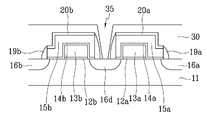
도 4에 도시된 바와 같이, 본 발명의 일 실시예에 따른 비휘발성 반도체 메모리 소자는 반도체 기판(11)과, 반도체 기판(11)상에 소정 간격 이격되어 형성된 제1 반도체 셀(10a) 및 제2 반도체 셀(10b)을 포함한다.As shown in FIG. 4, a nonvolatile semiconductor memory device according to an embodiment of the present invention may include a
이러한 제1 반도체 셀(10a)은 제1 게이트 절연막(12a), 제1 플로팅 게이트(13a), 제1 인터 폴리막(14a) 및 제1 컨트롤 게이트(15a)를 포함하고, 제2 반도체 셀(10b)은 제2 게이트 절연막(12b), 제2 플로팅 게이트(13b), 제2 인터 폴리막(14b) 및 제2 컨트롤 게이트(15b)를 포함한다.The
그리고, 제1 컨트롤 게이트(15a) 양측의 반도체 기판(11) 표면 내부에는 제1 소스 접합부(16a) 및 드레인 접합부(16d)가 형성되어 있고, 제2 컨트롤 게이트(15b) 양측의 반도체 기판 표면 내부에는 제2 소스 접합부(16b) 및 드레인 접합부(16d)가 형성되어 있다. 여기서 드레인 접합부(16d)는 제1 반도체 셀(10a) 및 제2 반도체 셀(10b)에 중첩하고 있다.The
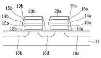
그리고, 제1 컨트롤 게이트(15a) 및 제2 컨트롤 게이트(15b) 위에 각각 제1 및 제2 캡 절연막(20a, 20b)이 형성되어 있고, 제1 및 제2 반도체 셀(10b)의 측벽에 질화막으로 이루어진 제1 및 제2 측벽 스페이서(19a, 19b)가 각각 형성되어 있다.First and second cap
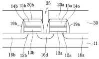
그리고, 제1 및 제2 캡 절연막(20a, 20b), 제1 및 제2 측벽 스페이서(19a, 19b) 및 반도체 기판(11)을 덮는 층간 절연막(30)이 형성되어 있고, 층간 절연막(30)에는 드레인 접합부(16d)를 노출하는 드레인 컨택홀(35)이 형성되어 있다.An
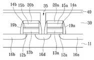
그리고, 이러한 층간 절연막(30) 내에 형성된 드레인 컨택홀(35)에 텅스텐 또는 구리로 이루어진 드레인 컨택(40)이 형성되어 드레인 접합부(16d)와 드레인 컨택(40)이 연결되어 있다.A
이러한 구성을 가지는 본 발명의 일 실시예에 따른 비휘발성 반도체 메모리 소자의 제조 방법에 대해 이하에서 상세히 설명한다.A method of manufacturing a nonvolatile semiconductor memory device according to an embodiment of the present invention having such a configuration will be described in detail below.
우선, 도 1에 도시된 바와 같이, 본 발명의 일 실시예에 따른 비휘발성 반도체 메모리 소자의 제조 방법은 반도체 기판(11) 위에 제1 반도체 셀(10a) 및 제2 반도체 셀(10b)을 소정 간격 이격되게 형성한다.First, as shown in FIG. 1, in the method of manufacturing a nonvolatile semiconductor memory device according to an embodiment of the present invention, a
여기서, 제1 반도체 셀(10a)은 제1 게이트 절연막(12a), 제1 플로팅 게이트(13a), 제1 인터 폴리막(14a) 및 제1 컨트롤 게이트(15a)를 포함한다.Here, the
제2 반도체 셀(10b)은 제2 게이트 절연막(12b), 제2 플로팅 게이트(13b), 제2 인터 폴리막(14b) 및 제2 컨트롤 게이트(15b)를 포함한다.The
제1 컨트롤 게이트(15a) 양측의 반도체 기판(11) 표면 내부에는 제1 소스 접합부(16a) 및 드레인 접합부(16d)를 형성한다. 그리고, 제2 컨트롤 게이트(15b) 양측의 반도체 기판(11) 표면 내부에는 제2 소스 접합부(16b) 및 드레인 접합부(16d)를 형성한다. 여기서 드레인 접합부(16d)는 제1 반도체 셀(10a) 및 제2 반도체 셀(10b)에 중첩한다.The
다음으로, 도 2에 도시된 바와 같이, 제1 컨트롤 게이트(15a) 및 제2 컨트롤 게이트(15b) 위에 각각 제1 및 제2 캡 절연막(20a, 20b)을 형성한다.Next, as shown in FIG. 2, first and second cap
그리고, 제1 및 제2 반도체 셀(10b)의 측벽에 질화막을 패터닝하여 각각 제1 및 제2 측벽 스페이서(19a, 19b)를 형성한다.The nitride films are patterned on sidewalls of the first and
다음으로, 도 3에 도시된 바와 같이, 제1 및 제2 캡 절연막(20a, 20b), 제1 및 제2 측벽 스페이서(19a, 19b) 및 반도체 기판(11)을 덮는 층간 절연막(30)을 형성한다.Next, as shown in FIG. 3, the
그리고, 층간 절연막(30)을 패터닝하여 상기 드레인 접합부(16d)를 노출하는 드레인 컨택홀(35)을 형성한다. 이 경우, 제1 및 제2 측벽 스페이서(19a, 19b)가 드레인 컨택홀(35)을 형성하기 위한 식각 공정 시 식각 방지막 역할을 한다.The
따라서, 제1 반도체 셀(10a) 및 제2 반도체 셀(10b) 간의 간격이 좁은 경우에도 제1 및 제2 반도체 셀(10b)을 손상하지 않고 드레인 컨택홀(35)을 형성하기 쉽다. 그러므로, 제1 반도체 셀(10a) 및 제2 반도체 셀(10b) 간의 간격이 좁도록 제1 반도체 셀(10a) 및 제2 반도체 셀(10b)을 형성할 수 있으므로 종래의 드레인 컨택홀(35)을 형성할 경우보다 전체 셀 사이즈를 줄일 수 있다.Therefore, even when the gap between the
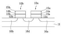
도 5에는 종래의 비휘발성 반도체 메모리 소자의 층간 절연막에 드레인 컨택홀(35) 및 드레인 컨택(40)을 형성한 상태를 도시하였다.5 illustrates a state in which the
도 5에 도시된 바와 같이, 종래에는 제1 반도체 셀(10a) 및 제2 반도체 셀(10b) 사이에 드레인 컨택홀(35)을 형성하는 경우 정렬 불량에 의해 제1 반도체 셀(10a) 및 제2 반도체 셀(10b)이 손상될 수 있으므로, 이를 방지하기 위해 제1 반도체 셀(10a) 및 제2 반도체 셀(10b) 사이의 간격을 넓게 형성하므로 전체 셀 사이즈가 증가한다. 그러나, 본 발명에서는 식각 방지막 역할을 하는 제1 및 제2 캡 절연막(20a, 20b), 제1 및 제2 측벽 스페이서(19a, 19b)를 형성함으로써 제1 반도체 셀(10a) 및 제2 반도체 셀(10b) 간의 간격이 좁도록 형성할 수 있어서 전체 셀 사이즈를 줄일 수 있다.As shown in FIG. 5, when the
다음으로, 도 4에 도시된 바와 같이, 층간 절연막(30) 내에 형성된 드레인 컨택홀(35)에 드레인 컨택(40)을 텅스텐 또는 구리를 이용하여 형성한다.Next, as shown in FIG. 4, the
본 발명의 다른 실시예에 따른 비휘발성 반도체 메모리 소자가 도 6에 도시되어 있다. 여기서, 앞서 도시된 도면에서와 동일한 참조 부호는 동일한 기능을 하는 동일한 부재를 가리킨다.A nonvolatile semiconductor memory device according to another embodiment of the present invention is shown in FIG. 6. Here, the same reference numerals as in the above-described drawings indicate the same members having the same function.
도 6에는 드레인 컨택홀(35)이 채널 분리형 셀 구조에 적용된 비휘발성 반도체 메모리 소자를 도시하였다.6 illustrates a nonvolatile semiconductor memory device in which a
도 6에 도시된 바와 같이, 식각 방지막 역할을 하는 제1 및 제2 캡 절연막(20a, 20b), 제1 및 제2 측벽 스페이서(19a, 19b)를 형성함으로써 제1 반도체 셀(10a) 및 제2 반도체 셀(10b) 간의 간격이 좁도록 제1 반도체 셀(10a) 및 제2 반도체 셀(10b)을 형성할 수 있어서 전체 셀 사이즈를 줄일 수 있다.As shown in FIG. 6, the
이상에서 본 발명의 바람직한 실시예에 대하여 상세하게 설명하였지만, 당해 기술 분야에서 통상의 지식을 가진 자라면 이로부터 다양한 변형 및 균등한 타 실시예가 가능하다는 점을 이해할 수 있을 것이다. 따라서, 본 발명의 권리 범위는 이에 한정되는 것은 아니고 다음의 청구범위에서 정의하고 있는 본 발명의 기본 개념을 이용한 당업자의 여러 변형 및 개량 형태 또한 본 발명의 권리범위에 속하는 것이다.Although the preferred embodiments of the present invention have been described in detail above, those skilled in the art will understand that various modifications and equivalent other embodiments are possible therefrom. Accordingly, the scope of the present invention is not limited thereto, and various modifications and improvements of those skilled in the art using the basic concept of the present invention as defined in the following claims also fall within the scope of the present invention.
본 발명에 따른 비휘발성 반도체 메모리 소자 및 그 제조 방법은 종래의 ETOX 셀 또는 채널 분리형 셀의 드레인 콘택을 식각 방지막 역할을 하는 제1 및 제2 캡 절연막, 제1 및 제2 측벽 스페이서를 형성함으로써 자기 정렬 방식으로 형성할 수 있고, 따라서, 전체 셀 사이즈를 줄일 수 있다는 장점이 있다.A nonvolatile semiconductor memory device and a method of manufacturing the same according to the present invention are characterized by forming first and second cap insulating films and first and second sidewall spacers, which serve as an etch barrier for drain contacts of conventional ETOX cells or channel-separated cells. It is possible to form in an alignment manner, and therefore, there is an advantage that the overall cell size can be reduced.
Claims (5)
Translated fromKoreanPriority Applications (2)
| Application Number | Priority Date | Filing Date | Title |
|---|---|---|---|
| KR1020030097919AKR100562318B1 (en) | 2003-12-26 | 2003-12-26 | Nonvolatile Semiconductor Memory Device and Manufacturing Method Thereof |
| US11/023,314US7247917B2 (en) | 2003-12-26 | 2004-12-27 | Nonvolatile semiconductor memory devices and methods of manufacturing the same |
Applications Claiming Priority (1)
| Application Number | Priority Date | Filing Date | Title |
|---|---|---|---|
| KR1020030097919AKR100562318B1 (en) | 2003-12-26 | 2003-12-26 | Nonvolatile Semiconductor Memory Device and Manufacturing Method Thereof |
Publications (2)
| Publication Number | Publication Date |
|---|---|
| KR20050066611A KR20050066611A (en) | 2005-06-30 |
| KR100562318B1true KR100562318B1 (en) | 2006-03-22 |
Family
ID=34698564
Family Applications (1)
| Application Number | Title | Priority Date | Filing Date |
|---|---|---|---|
| KR1020030097919AExpired - Fee RelatedKR100562318B1 (en) | 2003-12-26 | 2003-12-26 | Nonvolatile Semiconductor Memory Device and Manufacturing Method Thereof |
Country Status (2)
| Country | Link |
|---|---|
| US (1) | US7247917B2 (en) |
| KR (1) | KR100562318B1 (en) |
Families Citing this family (1)
| Publication number | Priority date | Publication date | Assignee | Title |
|---|---|---|---|---|
| US7776677B1 (en)* | 2009-03-30 | 2010-08-17 | Semiconductor Components Industries, Llc | Method of forming an EEPROM device and structure therefor |
Family Cites Families (6)
| Publication number | Priority date | Publication date | Assignee | Title |
|---|---|---|---|---|
| US5661054A (en)* | 1995-05-19 | 1997-08-26 | Micron Technology, Inc. | Method of forming a non-volatile memory array |
| JPH1117035A (en)* | 1997-06-24 | 1999-01-22 | Mitsubishi Electric Corp | Nonvolatile semiconductor memory device and method of manufacturing the same |
| US6271087B1 (en)* | 2000-10-10 | 2001-08-07 | Advanced Micro Devices, Inc. | Method for forming self-aligned contacts and local interconnects using self-aligned local interconnects |
| US6441428B1 (en)* | 2001-03-19 | 2002-08-27 | Micron Technology, Inc. | One-sided floating-gate memory cell |
| TW546778B (en)* | 2001-04-20 | 2003-08-11 | Koninkl Philips Electronics Nv | Two-transistor flash cell |
| US20040079984A1 (en)* | 2002-10-25 | 2004-04-29 | Hsuan-Ling Kao | Polysilicon self-aligned contact and a polysilicon common source line and method of forming the same |
- 2003
- 2003-12-26KRKR1020030097919Apatent/KR100562318B1/ennot_activeExpired - Fee Related
- 2004
- 2004-12-27USUS11/023,314patent/US7247917B2/ennot_activeExpired - Lifetime
Also Published As
| Publication number | Publication date |
|---|---|
| US20050139896A1 (en) | 2005-06-30 |
| US7247917B2 (en) | 2007-07-24 |
| KR20050066611A (en) | 2005-06-30 |
Similar Documents
| Publication | Publication Date | Title |
|---|---|---|
| CN100466293C (en) | Flash memory device and manufacturing method thereof | |
| KR101022666B1 (en) | Memory device and manufacturing method thereof | |
| US7776690B2 (en) | Method of forming a contact on a semiconductor device | |
| US7072210B2 (en) | Memory array | |
| US6777294B2 (en) | Method of forming a select line in a NAND type flash memory device | |
| US20040183124A1 (en) | Flash memory device with selective gate within a substrate and method of fabricating the same | |
| US20050062096A1 (en) | Nonvolatile semiconductor memory device and manufacturing method thereof | |
| US7491998B2 (en) | One time programmable memory and the manufacturing method thereof | |
| KR100275735B1 (en) | Method for manufacturing nor-type flash memory device | |
| US6555868B2 (en) | Semiconductor device and method of manufacturing the same | |
| US20080093678A1 (en) | NAND type non-volatile memory device and method of forming the same | |
| KR100606536B1 (en) | Nonvolatile Memory Device and Manufacturing Method Thereof | |
| US7800158B2 (en) | Semiconductor device and method of forming the same | |
| KR100562318B1 (en) | Nonvolatile Semiconductor Memory Device and Manufacturing Method Thereof | |
| US6159803A (en) | Method of fabricating flash memory | |
| US7408220B2 (en) | Non-volatile memory and fabricating method thereof | |
| KR100660283B1 (en) | Split gate type nonvolatile memory device and manufacturing method thereof | |
| KR20070049731A (en) | Flash memory and its manufacturing method | |
| KR100707674B1 (en) | Flash memory device and manufacturing method thereof | |
| US6414346B1 (en) | Semiconductor memory and manufacturing method thereof | |
| US6194271B1 (en) | Method for fabricating flash memory | |
| US7476929B2 (en) | Multi-bit stacked-type non-volatile memory | |
| KR100604532B1 (en) | Manufacturing method of nonvolatile memory device | |
| KR100285755B1 (en) | Non-volatile semiconductor memory device | |
| KR100593597B1 (en) | Manufacturing method of nonvolatile memory device |
Legal Events
| Date | Code | Title | Description |
|---|---|---|---|
| A201 | Request for examination | ||
| PA0109 | Patent application | St.27 status event code:A-0-1-A10-A12-nap-PA0109 | |
| PA0201 | Request for examination | St.27 status event code:A-1-2-D10-D11-exm-PA0201 | |
| R18-X000 | Changes to party contact information recorded | St.27 status event code:A-3-3-R10-R18-oth-X000 | |
| PG1501 | Laying open of application | St.27 status event code:A-1-1-Q10-Q12-nap-PG1501 | |
| E902 | Notification of reason for refusal | ||
| PE0902 | Notice of grounds for rejection | St.27 status event code:A-1-2-D10-D21-exm-PE0902 | |
| P11-X000 | Amendment of application requested | St.27 status event code:A-2-2-P10-P11-nap-X000 | |
| P13-X000 | Application amended | St.27 status event code:A-2-2-P10-P13-nap-X000 | |
| E701 | Decision to grant or registration of patent right | ||
| PE0701 | Decision of registration | St.27 status event code:A-1-2-D10-D22-exm-PE0701 | |
| GRNT | Written decision to grant | ||
| PR0701 | Registration of establishment | St.27 status event code:A-2-4-F10-F11-exm-PR0701 | |
| PR1002 | Payment of registration fee | St.27 status event code:A-2-2-U10-U11-oth-PR1002 Fee payment year number:1 | |
| PG1601 | Publication of registration | St.27 status event code:A-4-4-Q10-Q13-nap-PG1601 | |
| PN2301 | Change of applicant | St.27 status event code:A-5-5-R10-R13-asn-PN2301 St.27 status event code:A-5-5-R10-R11-asn-PN2301 | |
| PN2301 | Change of applicant | St.27 status event code:A-5-5-R10-R13-asn-PN2301 St.27 status event code:A-5-5-R10-R11-asn-PN2301 | |
| PR1001 | Payment of annual fee | St.27 status event code:A-4-4-U10-U11-oth-PR1001 Fee payment year number:4 | |
| PR1001 | Payment of annual fee | St.27 status event code:A-4-4-U10-U11-oth-PR1001 Fee payment year number:5 | |
| PR1001 | Payment of annual fee | St.27 status event code:A-4-4-U10-U11-oth-PR1001 Fee payment year number:6 | |
| PR1001 | Payment of annual fee | St.27 status event code:A-4-4-U10-U11-oth-PR1001 Fee payment year number:7 | |
| FPAY | Annual fee payment | Payment date:20130228 Year of fee payment:8 | |
| PR1001 | Payment of annual fee | St.27 status event code:A-4-4-U10-U11-oth-PR1001 Fee payment year number:8 | |
| FPAY | Annual fee payment | Payment date:20140217 Year of fee payment:9 | |
| PR1001 | Payment of annual fee | St.27 status event code:A-4-4-U10-U11-oth-PR1001 Fee payment year number:9 | |
| FPAY | Annual fee payment | Payment date:20150206 Year of fee payment:10 | |
| PR1001 | Payment of annual fee | St.27 status event code:A-4-4-U10-U11-oth-PR1001 Fee payment year number:10 | |
| PN2301 | Change of applicant | St.27 status event code:A-5-5-R10-R11-asn-PN2301 | |
| PN2301 | Change of applicant | St.27 status event code:A-5-5-R10-R14-asn-PN2301 | |
| PN2301 | Change of applicant | St.27 status event code:A-5-5-R10-R11-asn-PN2301 | |
| PN2301 | Change of applicant | St.27 status event code:A-5-5-R10-R14-asn-PN2301 St.27 status event code:A-5-5-R10-R11-asn-PN2301 | |
| PN2301 | Change of applicant | St.27 status event code:A-5-5-R10-R14-asn-PN2301 | |
| FPAY | Annual fee payment | Payment date:20160225 Year of fee payment:11 | |
| PR1001 | Payment of annual fee | St.27 status event code:A-4-4-U10-U11-oth-PR1001 Fee payment year number:11 | |
| FPAY | Annual fee payment | Payment date:20170308 Year of fee payment:12 | |
| PR1001 | Payment of annual fee | St.27 status event code:A-4-4-U10-U11-oth-PR1001 Fee payment year number:12 | |
| PR1001 | Payment of annual fee | St.27 status event code:A-4-4-U10-U11-oth-PR1001 Fee payment year number:13 | |
| PR1001 | Payment of annual fee | St.27 status event code:A-4-4-U10-U11-oth-PR1001 Fee payment year number:14 | |
| PC1903 | Unpaid annual fee | St.27 status event code:A-4-4-U10-U13-oth-PC1903 Not in force date:20200314 Payment event data comment text:Termination Category : DEFAULT_OF_REGISTRATION_FEE | |
| PC1903 | Unpaid annual fee | St.27 status event code:N-4-6-H10-H13-oth-PC1903 Ip right cessation event data comment text:Termination Category : DEFAULT_OF_REGISTRATION_FEE Not in force date:20200314 | |
| P22-X000 | Classification modified | St.27 status event code:A-4-4-P10-P22-nap-X000 |