KR100561908B1 - Sensor structure and its manufacturing method - Google Patents
Sensor structure and its manufacturing methodDownload PDFInfo
- Publication number
- KR100561908B1 KR100561908B1KR1020030097259AKR20030097259AKR100561908B1KR 100561908 B1KR100561908 B1KR 100561908B1KR 1020030097259 AKR1020030097259 AKR 1020030097259AKR 20030097259 AKR20030097259 AKR 20030097259AKR 100561908 B1KR100561908 B1KR 100561908B1
- Authority
- KR
- South Korea
- Prior art keywords
- sensor
- sensing
- temperature
- change
- film
- Prior art date
- Legal status (The legal status is an assumption and is not a legal conclusion. Google has not performed a legal analysis and makes no representation as to the accuracy of the status listed.)
- Expired - Fee Related
Links
Images


Classifications
- G—PHYSICS
- G01—MEASURING; TESTING
- G01N—INVESTIGATING OR ANALYSING MATERIALS BY DETERMINING THEIR CHEMICAL OR PHYSICAL PROPERTIES
- G01N27/00—Investigating or analysing materials by the use of electric, electrochemical, or magnetic means
- G01N27/26—Investigating or analysing materials by the use of electric, electrochemical, or magnetic means by investigating electrochemical variables; by using electrolysis or electrophoresis
- G01N27/28—Electrolytic cell components
- G01N27/40—Semi-permeable membranes or partitions
- G—PHYSICS
- G01—MEASURING; TESTING
- G01N—INVESTIGATING OR ANALYSING MATERIALS BY DETERMINING THEIR CHEMICAL OR PHYSICAL PROPERTIES
- G01N27/00—Investigating or analysing materials by the use of electric, electrochemical, or magnetic means
- G01N27/02—Investigating or analysing materials by the use of electric, electrochemical, or magnetic means by investigating impedance
- G01N27/04—Investigating or analysing materials by the use of electric, electrochemical, or magnetic means by investigating impedance by investigating resistance
- G01N27/12—Investigating or analysing materials by the use of electric, electrochemical, or magnetic means by investigating impedance by investigating resistance of a solid body in dependence upon absorption of a fluid; of a solid body in dependence upon reaction with a fluid, for detecting components in the fluid
- G01N27/125—Composition of the body, e.g. the composition of its sensitive layer
- G01N27/126—Composition of the body, e.g. the composition of its sensitive layer comprising organic polymers
- B—PERFORMING OPERATIONS; TRANSPORTING
- B82—NANOTECHNOLOGY
- B82B—NANOSTRUCTURES FORMED BY MANIPULATION OF INDIVIDUAL ATOMS, MOLECULES, OR LIMITED COLLECTIONS OF ATOMS OR MOLECULES AS DISCRETE UNITS; MANUFACTURE OR TREATMENT THEREOF
- B82B1/00—Nanostructures formed by manipulation of individual atoms or molecules, or limited collections of atoms or molecules as discrete units
Landscapes
- Chemical & Material Sciences (AREA)
- Health & Medical Sciences (AREA)
- Life Sciences & Earth Sciences (AREA)
- General Health & Medical Sciences (AREA)
- Immunology (AREA)
- Electrochemistry (AREA)
- Analytical Chemistry (AREA)
- Biochemistry (AREA)
- Chemical Kinetics & Catalysis (AREA)
- General Physics & Mathematics (AREA)
- Physics & Mathematics (AREA)
- Pathology (AREA)
- Crystallography & Structural Chemistry (AREA)
- Engineering & Computer Science (AREA)
- Nanotechnology (AREA)
- Molecular Biology (AREA)
- Investigating Or Analyzing Materials By The Use Of Fluid Adsorption Or Reactions (AREA)
Abstract
Translated fromKoreanDescription
Translated fromKorean도 1은 종래 기술에 의해 제작된 센서 구조체의 단면 구조도이다..1 is a cross-sectional structural view of a sensor structure manufactured by the prior art.
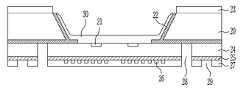
도 2는 본 발명의 실시예에 따른 센서 구조체의 단면 구조도이다.2 is a cross-sectional structural view of a sensor structure according to an embodiment of the present invention.
도 3a 내지 도 3g는 본 발명의 실시예에 따른 센서어레이 구조체의 제조방법을 단계별로 도시한 단면 구조도이다.3A to 3G are cross-sectional structural diagrams showing step by step a method of manufacturing a sensor array structure according to an embodiment of the present invention.
도 4는 본 발명의 실시예에 따른 화학 센서어레이를 장착한 측정기를 이용하여 화학종 및 그 농도 인지 방법의 순서를 보여주는 흐름도이다.Figure 4 is a flow chart showing the sequence of the chemical species and its concentration recognition method using a measuring instrument equipped with a chemical sensor array according to an embodiment of the present invention.
도 5는 본 발명에서 제작된 화학 센서의 온도 제어를 위해서 가열기 양단에 가해준 전압과 건조 공기 상태에서의 센서의 초기 저항 변화를 시간에 따라서 보여주는 곡선이다.5 is a curve showing the voltage applied to both ends of the heater for the temperature control of the chemical sensor manufactured in the present invention and the initial resistance change of the sensor in a dry air state with time.
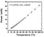
도 6은 본 발명의 실시예에 따른 센서어레이의 센서 구조체에 구비한 마이크로 가열기의 온도-소비전력 특성 곡선을 나타내는 그래프이다.6 is a graph showing a temperature-power consumption characteristic curve of the micro heater provided in the sensor structure of the sensor array according to an embodiment of the present invention.
도 7은 본 발명의 실험예에 따른 센서 어레이에서 전형적인 온도에 따른 감지 감도 변화를 보여준다.7 shows a change in sensing sensitivity with typical temperature in the sensor array according to the experimental example of the present invention.
도 8은 도 7의 실험예에 따른 센서 어레이에서 온도에 따른 감지 특성 변화를 매개 변수화하기 위하여 lnS(i)와 1/T 사이의 변화를 도식화한 그림이다.FIG. 8 is a diagram illustrating a change between lnS (i) and 1 / T in order to parameterize changes in sensing characteristics according to temperature in the sensor array according to the experimental example of FIG. 7.
도 9는 도 7의 실험예에서 감지 대상 화학종의 농도에 따른 반트호프 곡선의 기울기 변화를 나타낸 그래프이다.FIG. 9 is a graph illustrating a change in inclination of the Banthoff curve according to the concentration of the species to be detected in the experimental example of FIG. 7.
<도면의 주요 부분에 대한 부호의 설명><Explanation of symbols for the main parts of the drawings>
10 : 세라믹 기판 11, 21 : 감지 전극10:
12 : 감지막 13, 26 : 가열기 열선12:
14, 27 : 하부 보호막 20 : 반도체 기판14, 27: lower protective film 20: semiconductor substrate
22 : 기판 보호막 23 : 상부 보호막22: substrate protective film 23: upper protective film
24 : 맴브레인 절연막 25 : 보조 절연막24: membrane insulating film 25: auxiliary insulating film
28 : 감지 전극 패드 29 : 가열기 연결 패드
30 : 센서 감지막28: sensing electrode pad 29: heater connection pad
30: sensor detection film
본 발명은 센서구조체 및 그 제조방법에 관한 것이다.The present invention relates to a sensor structure and a method of manufacturing the same.
일반적으로 기체 상태에서 존재하는 화학종을 확인하는 것은 가스 크로마토그래피나 질량분석기와 같은 화학 분석 장비를 이용하여 수행하여 왔다. 최근에는 이러한 화학종 분석을 휴대형 장치를 이용하여 수행함으로써 대기 오염, 음식물 품질 관리, 유해 미생물 감염, 화생방 물질 오염 여부를 실시간에 현장에서 확인하려는 욕구가 증대되고 있다. 이러한 관점에서 기존의 화학 분석 장비를 소형화 하는 노력들이 있어 왔다.In general, identification of chemical species present in the gas phase has been performed using chemical analysis equipment such as gas chromatography or mass spectrometry. In recent years, such species analysis using a portable device has increased the need for real-time on-site checking for air pollution, food quality control, harmful microbial infections, and biological and chemical contamination. In this regard, efforts have been made to miniaturize existing chemical analysis equipment.
하지만, 이러한 분석 장비는 소형화에 한계를 가지므로 현재에는 소형의 화학 센서를 이용하여 휴대형 분석 장치 개발이 활발히 진행되어 왔다. 특히, 기존의 단일 센서가 가지는 특정 피검출물에 감지 특성을 보다 다양한 화학종을 감지하기 위하여 다수의 화학 센서로 구성된 센서어레이를 이용한 전자후각 (electronic nose) 장치를 활발히 개발하고 있다.However, since such an analytical equipment has a limitation in miniaturization, the development of a portable analytical device using a small chemical sensor has been actively progressed. In particular, in order to detect various chemical species with specific detection characteristics of a specific object of the existing single sensor, an electronic nose device using a sensor array composed of a plurality of chemical sensors has been actively developed.
전자후각 시스템에 주로 이용되어온 센서기술로는 SnO2로 대표되는 산화물 반도체 기술, bulk acoustic을 이용하는 QCM (quartz crystal microbalance), surface acoustic을 이용한 SAW (surface acoustic wave) 소자, 고분자의 전기 전도도를 응용한 전도성 고분자 소자, 전도성 입자와 비전도성 고분자로 구성된 고분자 혼합체 소자, 단일 분자의 흡수 파장 변화를 이용한 colorimetric 기술 등이 있다.Sensor technologies that have been used mainly in electronic olfactory systems include oxide semiconductor technology represented by SnO2 , quartz crystal microbalance (QCM) using bulk acoustic, surface acoustic wave (SAW) devices using surface acoustic, and electrical conductivity of polymers. Conductive polymer devices, polymer composite devices composed of conductive particles and non-conductive polymers, and colorimetric technology using changes in absorption wavelength of a single molecule.
이러한 다양한 센서기술 중에서 소재 개조가 용이한 유기 고분자를 이용한 전도성 고분자 및 고분자 혼합체 기술이 다양한 전자후각 센서어레이를 만들어 낼 수 있다는 장점을 갖는다. 하지만 이러한 유기물 센서 소재는 일반적으로 온도와 습도에 민감한 감지 특성 변화를 보여주므로 항온 및 항습의 조건을 유지하여야 하는 문제점이 있다.Among these various sensor technologies, conductive polymers and polymer mixture technologies using organic polymers, which are easy to modify materials, have the advantage of producing various electronic olfactory sensor arrays. However, such organic sensor material generally shows a change in sensing characteristics sensitive to temperature and humidity, there is a problem to maintain the conditions of constant temperature and humidity.
이하, 도 1을 참조하여 종래 기술에 의하여 제작된 화학센서를 설명한다.Hereinafter, a chemical sensor manufactured according to the prior art will be described with reference to FIG. 1.
도 1의 화학센서는 세라믹 기판(10)의 전면에는 감지전극(11)과 센서 감지막(12)을 형성하고, 뒷면에는 가열기 열선(13)과 하부보호막(14)를 형성하는 구조를 가지고 있다.The chemical sensor of FIG. 1 has a structure in which a
유기 고분자를 이용한 전도성 고분자 및 고분자 혼합체 기술은 상온에서도 작동이 가능하지만 온도에 따라서 감지 특성이 변화하므로 일정한 감지 패턴을 얻어내기 위해서는 항온 조건을 구현하여야 한다. 일반적으로 40oC 내외의 항온 조건을 만들어서 측정함으로써 외부의 온도 변화에 따른 측정 오차를 최소화 할 수 있다. 하지만, 종래기술에 의한 화학센서는 외부로 상당한 열손실을 유발하므로 온도 제어가 요구되는 초소형 전자후각 장비를 만들기에는 소비전력이 너무 크다는 문제점이 있었다.The conductive polymer and the polymer mixture technology using the organic polymer can operate at room temperature, but the sensing characteristics change according to the temperature, so that a constant temperature condition must be implemented to obtain a constant sensing pattern. In general, it is possible to minimize the measurement error caused by the external temperature change by measuring by making a constant temperature around 40° C. However, the chemical sensor according to the prior art causes a significant heat loss to the outside, there is a problem that the power consumption is too large to make a micro electronic olfactory equipment that requires temperature control.
또한, 센서 기판 온도에 따라 감지 화학종과 센서물질 사이의 물리화학적인 상호작용이 변화하므로 온도에 따라서 센서어레이의 감지 패턴이 변화하고, 온도에 따른 감지 특성 변화 측정을 통하여 상호작용에 대한 열역학적인 매개변수를 도출할 수 있다. (Schierbaum et al, Sensora and Actuators A, 1992, 31, 130) 이러한 결과는 선행연구(미국특허번호 제5,911,872호)에서도 잘 보여준다.In addition, since the physicochemical interaction between the sensing species and the sensor material changes according to the temperature of the sensor substrate, the sensing pattern of the sensor array changes according to the temperature, and the thermodynamic response Parameters can be derived. (Schierbaum et al, Sensora and Actuators A, 1992, 31, 130) These results are also shown in previous studies (US Pat. No. 5,911,872).
하지만 온도에 따른 측정을 종래의 기판으로 수행하기 위해서는 온도 안정화를 위하여 10분 이상의 시간이 소모되므로 휴대형 초소형 전자후각 장치에서는 전력 소비가 많고, 센서 안정화에 필요한 기체량 소모가 많아서 현실적으로 구현하기 어려웠다.However, in order to perform the temperature-based measurement with a conventional substrate, since the time is more than 10 minutes for temperature stabilization, the portable microelectronic olfactory device consumes a lot of power and has a large amount of gas required for sensor stabilization.
상술한 문제점을 해결하기 위하여 안출된 것으로, 본 발명의 목적은 열손실 을 최소화하기 위하여 멤브레인 위에 구현된 일체형 미소 가열기를 이용하여 유기 고분자 혼합체로 구성된 센서를 능동적으로 온도를 제어하고 온도변화에 따른 감지 패턴을 이용해 화학종 및 그 농도를 정확히 알아내는 방법에 관한 것이다.In order to solve the above problems, an object of the present invention is to actively control the temperature of the sensor composed of the organic polymer mixture by using an integrated micro-heater implemented on the membrane in order to minimize the heat loss and to detect the temperature change It is about how to accurately determine the species and its concentration using the pattern.
본 발명의 다른 목적은 일체형 저전력 미소 가열기를 이용하여 센서소재의 온도를 능동적으로 제어하고, 이를 이용하여 하나 이상의 고분자 혼합체 센서로 구성된 화학 센서어레이에서 온도에 감지 패턴 변화를 이용하여 화학종 및 그 농도를 정확히 얻어내는 방법을 제공하는 것이다.Another object of the present invention is to actively control the temperature of the sensor material by using an integrated low-power micro heater, using the chemical pattern array in the chemical sensor array consisting of one or more polymer mixed sensor using the chemical species and its concentration Is to provide a way to get
본 발명의 또다른 목적은 낮은 전력으로 빠르게 온도 제어가 가능하게 하여 온도에 따른 감지 특성 측정을 통하여 피분석 화학종과 그 농도를 신뢰성 높게 인지하는 방법을 제공하는 것이다.
Still another object of the present invention is to provide a method for reliably recognizing an analyte species and its concentration through measurement of sensing characteristics according to temperature by enabling temperature control at low power.
상기 기술적 과제를 달성하기 위한 기술적 수단으로서, 본 발명의 일측면은 우물 구조를 갖는 멤브레인 구조; 상기 우물 구조 내부에 배치되는 적어도 1쌍의 감지 전극; 상기 감지 전극 상부에 형성되는, 전도성 입자와 비전도성 고분자의 혼합체로 된 센서 감지막; 및 상기 우물 구조 내부에 온도를 제어하기 위한 가열기를 구비하되, 피분석물 분석은 상기 센서 감지막을 이용하여 적어도 2개의 온도에서 화학종 노출에 따른 상기 센서 감지막들의 물리량 변화를 측정하여 수행되는 센서 구조체를 제공한다.As a technical means for achieving the above technical problem, one side of the present invention is a membrane structure having a well structure; At least one pair of sensing electrodes disposed within the well structure; A sensor sensing film formed of a mixture of conductive particles and non-conductive polymer formed on the sensing electrode; And a heater for controlling a temperature inside the well structure, wherein analyte analysis is performed by measuring a change in physical quantity of the sensor detection films according to chemical species exposure at at least two temperatures using the sensor detection film. Provide a structure.
본 발명의 다른 측면은 반도체 기판의 일면에 감지전극을 형성하는 단계; 상기 반도체 기판의 상기 일면에 상기 멤브레인에 해당하는 절연막을 형성하는 단계;Another aspect of the invention comprises the steps of forming a sensing electrode on one surface of the semiconductor substrate; Forming an insulating film corresponding to the membrane on the one surface of the semiconductor substrate;
상기 멤브레인 상부에 가열기를 형성하는 단계; 상기 반도체 기판의 타면에서부터 식각하여 상기 감지전극이 드러나도록 하여 우물 구조를 형성하는 단계; 및Forming a heater on the membrane; Forming a well structure by etching the other surface of the semiconductor substrate to expose the sensing electrode; And
상기 우물 구조의 내부에, 전도성 입자와 비전도성 고분자의 혼합체로 된 센서 감지막을 형성하는 단계를 구비하되, 피분석물 분석은 상기 센서 감지막을 이용하여 적어도 2개의 온도에서 화학종 노출에 따른 상기 센서 감지막들의 물리량 변화를 측정하여 수행되는 센서 구조체의 제조 방법을 제공한다.And forming a sensor sensing film made of a mixture of conductive particles and non-conductive polymer in the well structure, wherein analyte analysis uses the sensor sensing film to detect the sensor according to chemical species exposure at at least two temperatures. A method of manufacturing a sensor structure is performed by measuring a change in physical quantity of sensing films.
이하, 첨부한 도면들을 참조하여 본 발명의 바람직한 실시예를 상세히 설명한다. 그러나, 본 발명의 실시예들은 여러가지 형태로 변형될 수 있으며, 본 발명의 범위가 아래에서 상술하는 실시예들로 인하여 한정되는 식으로 해석되어 져서는 안된다. 본 발명의 실시예들은 당업계에서 평균적 지식을 가진 자에게 본 발명을 보다 완전하게 설명하기 위해 제공되는 것이다. 도면에서 막 또는 영역들의 크기 또는 두께는 명세서의 명확성을 위하여 과장된 것이다.Hereinafter, exemplary embodiments of the present invention will be described in detail with reference to the accompanying drawings. However, embodiments of the present invention may be modified in various forms, and the scope of the present invention should not be construed as being limited by the embodiments described below. Embodiments of the present invention are provided to more fully explain the present invention to those skilled in the art. In the drawings, the size or thickness of films or regions is exaggerated for clarity.
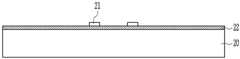
도 2는 화학종 인식 방법에 사용되는 센서 어레이의 단위 센서구조체의 개략적인 단면 개요도이다.2 is a schematic cross-sectional schematic diagram of a unit sensor structure of a sensor array used in a chemical species recognition method.
본 센서 구조체는 우물 구조를 갖는 멤브레인 구조와, 우물 구조 내부에 배치되는 적어도 1쌍의 감지 전극(21)과, 감지 전극(21) 상부에 형성되는, 전도성 입자와 비전도성 고분자의 혼합체로 된 센서 감지막(30)과, 우물 구조 내부에 온도를 제어하기 위한 가열기를 구비하되, 피분석물 분석은 센서 감지(30)막을 이용하여 적어도 2개의 온도에서 화학종 노출에 따른 상기 센서 감지(30)막들의 물리량 변화를 측정하여 수행된다.The sensor structure includes a membrane structure having a well structure, at least one pair of
이하, 도 3a 내지 도 3G를 참조하여 본 발명의 실시예에 따른 센서어레이 구조체의 제조방법을 단계별로 구체적으로 살펴보면 다음과 같다.Hereinafter, a method of manufacturing a sensor array structure according to an embodiment of the present invention will be described in detail with reference to FIGS. 3A to 3G as follows.
(기판 보호막(21) 형성)(
도 3a를 참조하면, 반도체 기판(20)과 감지 전극(21) 사이의 전기적인 단전을 위하여 먼저 반도체 기판(20) 일면에 기판 보호막(22)을 형성한다. 반도체 기판(20)은 양면 폴리싱(polishing)된 반도체 기판(20)이 바람직하고, 일반적인 예로써 실리콘 기판 또는 갈륨-비소(GaAs) 기판 등이 있다. 기판 보호막(22)은 100 nm 두께의 산화막을 형성하는 것이 바람직하다.Referring to FIG. 3A, the
(감지 전극(21) 형성)(Sense Electrode 21 Formation)
도 3b를 참조하면, 반도체 기판(20)의 일면에 위치한 기판 보호막(22) 위에 금속 물질을 증착한 후 금속 물질을 패터닝(patterning)하여 감지전극 형상을 형성한다. 감지 전극(21)은 센서 소재의 물리적인 변화를 감지하기 위해 사용된다. 사용될 수 있는 소재로는 예를 들면 금(Au) 뿐만 아니라 백금(Pt), 알루미늄(Al), 몰리브덴(Mo), 은(Ag) TiN, 텅스텐(W), 루테늄(Ru), 이리듐(Ir) 또는 결정성 실리콘(p-Si) 등이다. 금속 물질을 증착하기 이전에 기판 보호막(22)과 감지 전극(21) 소재 간의 접착력(adhesion)을 증가시키는 물질을 증착할 수도 있다. 접착력을 증가시키는 물질은 예를 들면 크롬(Cr) 또는 타이타늄(Ti)이 있다. 접착력 을 증가시키는 물질의 두께는 5 nm 로, 감지 전극 물질의 두께는 100 nm 내외로 형성되는 것이 바람직하다. 패터닝은 일례로 에칭 공정을 사용하여 이루어질 수도 있으며, 다른 일례로 리프트-오프(lift-off) 공정을 사용하여 이루어질 수도 있다.Referring to FIG. 3B, a metal material is deposited on the
(감지영역의 기판보호막(21) 제거)(Removing substrate
도 3c를 참조하면, 감지영역의 기판보호막(22)을 미리 제거하는 단계가 필요하다. 기판보호막(22)의 제거는 습식 식각을 이용하거나 건식 식각을 이용할 수도 있다. 감지영역의 기판보호막(22)을 제거하는 이유는 후속공정에서 벌크 실리콘을 제거한 후, 형성된 우물 구조 내부에 센서 용액을 이용해 감지막을 형성할 때, 감지막과 감지전극 사이의 전기적 연결을 위함이다.Referring to FIG. 3C, it is necessary to remove the substrate
(맴브레인 절연막(24), 보조 절연막(25) 및 미소 가열기 열선(26) 형성)(Formation of
도 3d를 참조하면, 감지 전극(21)과 미소 가열기 사이의 전기적인 간섭을 배제하고, 우물 구조에서 바닥을 물리적으로 지탱하는 맴브레인 박막을 형성하기 위하여 맴브레인 절연막(24)와 보조 절연막(25)을 형성한다. 바람직하게는 1.5um 실리콘 질화막과 300nm 실리콘 산화막을 증착한다. 보조 절연막(25)은 맴브레인 절연막(24)에 의해서 형성되는 응력(stress)을 상쇄 해주는 역할도 수행한다.Referring to FIG. 3D, the
다음으로, 보조 절연막(25) 위에 금속 물질을 증착한 후 금속 물질을 패터닝(patterning)하여 미소 가열기 열선(26)을 제조하여 센서 소재의 온도 제어에 이용한다. 사용 가능한 물질은 예를 들면 금(Au) 뿐만 아니라 백금(Pt), 알루미늄(Al), 몰리브덴(Mo), 은(Ag) TiN, 텅스텐(W), 루테늄(Ru), 이리듐(Ir) 또는 다결정 실리콘(p-Si) 등이다.Next, after depositing a metal material on the auxiliary insulating
금속 물질을 증착하기 이전에 보조 절연막(25)과 금속 물질 간의 접착력 (adhesion)을 증가시키는 물질을 증착할 수도 있다. 접착력을 증가시키는 물질은 예를 들면 크롬(Cr) 또는 타이타늄(Ti)이 있다. 접착력을 증가시키는 물질의 두께는 5nm 로, 금속 물질의 두께는 100nm로 형성될 수 있다. 패터닝은 일례로 에칭 공정을 사용하여 이루어질 수도 있으며, 다른 일례로 리프트-오프(lift-off) 공정을 사용하여 이루어질 수도 있다. 바람직하게는 가열기 형성시 온도를 측정할 수 있는 온도 센서를 동시에 제작하는 것이 바람직하고, 이러한 역할을 동시에 수행할 수 있는 대표적인 소재로는 백금(Pt), 다결정성 실리콘(p-Si) 등이 있다.Prior to depositing the metal material, a material for increasing the adhesion between the auxiliary insulating
(하부 보호막(27) 및 상부 보호막(23) 형성)(Formation of the lower protective film 27 and the upper protective film 23)
도 3e를 참조하면, 가열기 열선(26)을 외부의 물리적인 공격과 전기적인 합선으로부터 보호하기 위하여 하부 보호막(27)을 형성한다. 일례로 두께가 100nm와 300nm 사이인 실리콘 산화막일 수 있다. 다음으로, 실리콘 벌크 식각의 마스크로 사용 가능한 상부 보호막(23)을 증착하고 패터링 한다. 이방성 습식 식각(anisotropic wet etching)을 이용하여 벌크 실리콘을 식각하는 경우에 식각 용액에 식각이 거의 되지 않는 500 nm 내외의 실리콘 산화막이나 실리콘 질화막인 것이 바람직하다.Referring to FIG. 3E, the lower protective layer 27 is formed to protect the
(감지 전극 패드(28) 및 가열기 연결 패드(29) 오픈)(
도 3f를 참조하면, 외부에서 전기적인 연결이 가능하도록 감지전극 패드(28) 및 가열기의 패드(29)를 건식 식각을 통해 개방한다.Referring to FIG. 3F, the
(반도체 기판(22) 벌크 식각과 노출된 반도체 기판 측면에 기판 절연체(22) 형성)(
도 3g를 참조하면, 열손실을 최소화 하고 센서용액을 담을 수 있는 우물형 구조체를 형성하기 위하여 전극이 형성된 반대편에서 반도체 기판(20)을 벌크 식각한다. 실리콘 기판을 사용한 경우에는, 일례로 KOH 또는 TMAH(tri-methyl ammonium hydroxide)를 식각액(etchant)으로 사용하여 실리콘 기판을 이방성 습식 식각할 수 있다. 이때 형성된 우물 구조는 추후의 공정에서 전극 위에 떨어뜨리는 센서 물질(30)이 퍼지는 것을 방지하는 기능과 일정한 두께의 센서 물질(30)을 재현성 있게 만들 수 있도록 하는 기능을 수행한다. 또한 맴브레인 절연막(24)와 보조 절연막(25)을 갖는 우물 구조는 우물 바닥에 해당하는 기판이 완전히 제거됨으로써, 가열기 열선(26)가 센서 물질(30)을 가열할 때 열손실이 줄어들게 되므로, 미소 가열기가 저전력에서 동작할 수 있다.Referring to FIG. 3G, the
반도체 기판(22)의 벌크 식각으로 인하여 우물 구조의 내부에 반도체 기판(22)을 보호하는 기판 절연체로 보호되지 않고 외부로 노출된 반도체 기판 측면이 형성되므로, 이를 하드 마스크(hard mask) 공정을 사용하여 기판 보호막(22)을 형성하여 준다. 하드 마스크 공정은 우물의 측벽에 대응하는 부분이 구멍난 하드 마스크를 기판의 타면과 접한 후 절연체를 증착함으로써, 절연체를 우물의 측벽에만 선택적으로 증착하는 공정이다. 바람직한 박막 소재로는 실리콘 산화물 또는 알루미늄 산화물 등이 있다.Due to the bulk etching of the
(센서 감지막의 형성)(Formation of sensor sensing film)
다음으로, 우물 구조 내부에 피분석 화학종에 반응하여 물리량 변화를 유발할 수 있는 센서 감지막을 형성해 주어야 한다. 일반적으로 많이 이용되는 물리량으로는 화학종의 흡착으로 유발되는 질량 또는 전기 전도도 등이 있다.Next, a sensor sensing film may be formed inside the well structure, which may cause a change in physical quantity in response to the analyte species. In general, the physical quantities used are mass or electrical conductivity caused by the adsorption of chemical species.
질량을 감지하는 센서로는 QCM 또는 SAW 소자들이 있고, 전기 전도도를 측정하는 센서로는 산화물 반도체, 전도성 고분자, 전도성 입자-유기물 혼합체 센서를 이용한 소자 들이 있다. 이러한 센서 중에서 외부 환경에 대한 안정성이 뛰어나고, 다양한 센서 제조가 가능하고, 초소형 전자후각 시스템에 적합한 전도성 입자-유기물 혼합체 소재를 이용하여 센서 어레이를 제조하는 것이 바람직하다.Mass sensing sensors include QCM or SAW devices, and electrical conductivity sensors include oxide semiconductors, conductive polymers, and conductive particle-organic hybrid sensors. Among these sensors, it is desirable to manufacture a sensor array using a conductive particle-organic mixture material which is excellent in stability to the external environment, is capable of manufacturing various sensors, and which is suitable for a microelectronic olfactory system.
전도성 입자-유기물 혼합체 센서는 전기 전도성 입자를 전기 전도도가 없는 유기물 매체에 분산함으로써 제한적인 전기 전도 경로를 가지게 하고 피분석 화학종이 센서 소재에 침입하면 혼합체의 저항이 변화하는 원리를 이용한다. 예를 들어, 전도성 금속 입자로는 금, 은, 팔라듐, 구리로 구성된 나노 입자들이 있다. 전도성 입자-유기물 혼합체 센서는 전도성 카본 블랙 입자와 비전도성 고분자로 이루어진 카본 블랙-고분자 혼합체와 전도성 금속 입자와 이들 표면과 화학 반응하여 유기물로 구성된 표면 보호형 금속 입자 소재들이 있다.The conductive particle-organic mixture sensor utilizes the principle that the resistance of the mixture changes as the analyte species invade the sensor material by dispersing the electrically conductive particles in an organic medium without electrical conductivity. For example, conductive metal particles include nanoparticles composed of gold, silver, palladium, and copper. The conductive particle-organic mixture sensor includes a carbon black-polymer mixture made of conductive carbon black particles and a non-conductive polymer, conductive metal particles, and surface protective metal particle materials composed of organic materials by chemically reacting with these surfaces.
이하에서는 전도성 카본 블랙 입자와 비전도성 고분자를 이용하여 제작한 혼합체 센서의 경우를 설명한다. 다양한 화학 센서 조합을 구성하기 위하여 비전도성 고분자의 종류를 바꿀 수 있고, 서로 다른 고분자들이 혼합된 혼성 고분자를 이용하거나 단분자 유기물을 첨가해 주어서 비전도성 고분자의 특성을 변화시킬 수 있다.Hereinafter, a case of a mixed sensor manufactured using conductive carbon black particles and a nonconductive polymer will be described. In order to construct various chemical sensor combinations, the types of nonconductive polymers can be changed, and the properties of the nonconductive polymers can be changed by using hybrid polymers in which different polymers are mixed or by adding monomolecular organic materials.
대표적인 비전도성 고분자 소재로는 표 1에 나열한 물질들이고, 대표적인 첨가제로는 di(2-ethylhexyl) phhalate or dioctyl phthalate, di(ethylene glycol) dibenzoate 등이 있다.Representative non-conductive polymer materials include those listed in Table 1, and representative additives include di (2-ethylhexyl) phhalate or dioctyl phthalate and di (ethylene glycol) dibenzoate.

이하, 전도성 카본 블랙 입자와 비전도성 고분자를 이용하여 제작한 센서 감지막의 형성 과정을 상세히 설명한다.Hereinafter, a process of forming the sensor sensing film manufactured using the conductive carbon black particles and the nonconductive polymer will be described in detail.
먼저, 비전도성 고분자를 일반적인 유기 용매에 잘 녹인다. 대표적인 용매로는 사염화탄소, THF, 벤젠, 이염화탄소, 톨루엔, 에칠 알콜 등이 있다. 잘 녹지 않 는 고분자를 효과적으로 녹이기 위해서는 50oC 정도로 가열하고 용액을 교반하여 주었다. 이렇게 용해된 고분자 용액에 카본 블랙을 넣고 초음파로 10분 이상 충격을 주어서 카본 블랙 입자가 용액에 균일하게 분산되도록 한다. 일반적으로 사용하는 용매의 양은 10ml, 카본 블랙은 20mg, 고분자는 80mg을 이용한다.First, the nonconductive polymer is well dissolved in a general organic solvent. Representative solvents include carbon tetrachloride, THF, benzene, carbon dichloride, toluene, ethyl alcohol and the like. In order to effectively dissolve the poorly dissolved polymer was heated to about 50o C and the solution was stirred. The carbon black is added to the dissolved polymer solution, and the carbon black particles are impacted with ultrasonic waves for at least 10 minutes to uniformly disperse the carbon black particles in the solution. Generally, 10 ml of solvent, 20 mg of carbon black, and 80 mg of polymer are used.
카본 블랙의 양은 고분자와 카본 블랙으로 구성된 전체 센서 중량에 대하여 10 - 30%가 되도록 하고, 최적의 센서는 10k - 10M 저항을 갖는 것이 바람직하다.The amount of carbon black is 10 to 30% of the total sensor weight composed of polymer and carbon black, and the optimum sensor preferably has a 10k-10M resistance.
한편, 첨가제를 사용하는 경우에는 고분자와 첨가제 무게의 합이 80mg이 되도록 하고 첨가제의 중량비가 10 - 60%가 되는 범위에서 센서를 제작할 수 있다. 이렇게 준비된 혼합체 용액을 이용해 감지막을 형성하는 방법으로는 마이크로 피펫을 이용하여 방울을 감지 전극에 떨어뜨리는 디스펜싱(dispensing) 방법, 감지전극 기판을 용액에 넣은 후 빼서 말리는 침지(dipping)법, 감지 전극 위에 용액을 떨어뜨린 후 기판을 회전시키는 스핀코팅(spin coating)법 등이 있다. 일체형 센서어레이를 이용하는 경우에는 우물 구조 내부에 서로 다른 용액을 떨어뜨리는 디스펜싱법이 바람직하다.On the other hand, in the case of using the additive, the sum of the weight of the polymer and the additive may be 80 mg, and the sensor may be manufactured in the range in which the weight ratio of the additive is 10-60%. As a method of forming a sensing film using the prepared mixture solution, a dispensing method of dropping droplets onto a sensing electrode using a micro pipette, a dipping method of putting a sensing electrode substrate into a solution and then drying it out, and sensing electrode There is a spin coating method that rotates a substrate after dropping a solution thereon. In the case of using the integrated sensor array, a dispensing method in which different solutions are dropped into the well structure is preferable.
다른 센서 감지막의 제조 방법으로는 -SH (thiol) 그룹으로 표면이 안정화된 금 나노 입자를 톨루엔과 같은 용매에 녹인 용액을 사용하여 센서 감지막을 제조할 수 있다. 위에서 제시한 제조 방법들을 사용하여 제조 한다.As another method of manufacturing a sensor sensing film, a sensor sensing film may be manufactured using a solution in which gold nanoparticles whose surface is stabilized with a -SH (thiol) group are dissolved in a solvent such as toluene. It is prepared using the preparation method described above.
제작된 화학 센서 어레이는 유체의 흐름을 제어하는 부품과 유체가 흐르는 유로를 이용하여 외부 기체 시료를 능동적으로 센서 소재와 반응시킬 수 있는 측정기 안에 장착한다. 기본적으로 기체 시료 측정기는 우물 구조를 갖는 센서 어레이 상부에 판을 부착시켜서 센서 소재가 밀폐된 공간 안에 놓이게 하고, 한쪽 편에서는 유체의 유입이 가능한 입구가 있고 반대편으로는 유체가 빠져 나가도록 한다. 이렇게 유입된 유체 시료는 감지 전극 위에 형성된 다수의 감지막들과 동일한 조건에서 상호작용 할 수 있는 조건을 마련해 주는 것이 바람직하다.The fabricated chemical sensor array is mounted inside a measuring instrument that can actively react an external gas sample with the sensor material using components that control the flow of fluid and flow paths. Basically, a gas sampler attaches a plate on top of a well-arranged sensor array so that the sensor material is placed in a confined space, and on one side there is an inlet through which the fluid can enter and the fluid on the other side exits. The introduced fluid sample is preferably provided with a condition that can interact with the plurality of sensing films formed on the sensing electrode under the same conditions.
도 4는 본 발명의 실시예에 따른 화학 센서어레이를 장착한 측정기를 이용하여 화학종 및 그 농도 인지 방법의 순서를 보여주는 흐름도이다.Figure 4 is a flow chart showing the sequence of the chemical species and its concentration recognition method using a measuring instrument equipped with a chemical sensor array according to an embodiment of the present invention.
측정이 시작되면(S101), 건조 공기 또는 질소를 측정기에 흘려주는 상태에서온도를 설정하고 안정화 시키고(S103), 센서의 초기 저항을 측정한다(S105). 그런다음 분석시료를 주입하고(S107), 센서 저항을 측정하고 감도를 저장한다(S109). 다음으로, 세로운 온도를 설정할 필요가 있으면 다시 온도를 설정하고 안정화 시키는 S103단계로 진행하고, 새로운 온도를 설정할 필요가 없으면, 패턴인식을 수행하는 단계(S113)로 진행한다.When the measurement is started (S101), the temperature is set and stabilized in a state of flowing dry air or nitrogen to the measuring instrument (S103), and the initial resistance of the sensor is measured (S105). Then the sample is injected (S107), the sensor resistance is measured and the sensitivity is stored (S109). Next, if it is necessary to set a new temperature, the process proceeds to step S103 to set and stabilize the temperature again, and if it is not necessary to set a new temperature, the process proceeds to step S113 of performing pattern recognition.
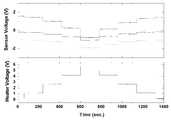
도 5는 본 발명에서 제작된 화학 센서의 온도 제어를 위해서 가열기 양단에 가해준 전압(하단)과 건조 공기 상태에서의 센서의 초기 저항(상단) 변화를 시간에 따라서 보여주는 그래프이다.Figure 5 is a graph showing the change in voltage (lower) applied to the heater (end) and the initial resistance (top) of the sensor in the dry air state over time for temperature control of the chemical sensor manufactured in the present invention.
도 5를 참조하면, 20 - 60oC 영역의 온도에서 센서 어레이가 1초 내외로 빠르게 온도에 대한 안정화가 관측되고, 미리 흡착된 시료를 제거하는데 걸리는 시간, 초기 저항값이 일정해 지는 시간은 수분 정도가 소요된다. 따라서, 가열을 하지 않은 상태에서 초기 저항을 안정화 시킨 후 측정하기 바로 전에 온도를 설정하는 것이 전력 소비를 줄일 수 있다.Referring to FIG. 5, the temperature of the sensor array is rapidly stabilized to about 1 second at a temperature in the region of 20-60o C, the time taken to remove the pre-adsorbed sample, and the time that the initial resistance becomes constant. It takes a few minutes. Thus, setting the temperature just before measurement after stabilizing the initial resistance without heating can reduce power consumption.
또한 초기 저항을 빠른 시간에 안정화하기 위해서 센서 소재 온도를 가열기를 이용해 가열하면 흡착된 시료의 탈착을 촉진시킬 수 있다. 안정화가 된 후에는 초기 저항을 측정하고, 일정한 시간동안 시료를 측정기에 주입한 후의 저항 변화를 측정한다. 이렇게 측정된 초기 및 감지 저항을 이용하여 각 센서에서의 피감지 시료에 대한 감도를 계산하여 저장한다. 일반적으로 감지 감도는 초기 저항에 대하여 변화한 저항값의 백분율로 표시한다.In addition, in order to stabilize the initial resistance in a short time, the temperature of the sensor material is heated with a heater to promote desorption of the adsorbed sample. After stabilization, the initial resistance is measured, and the resistance change after measuring the sample for a certain time. The sensitivity of the detected sample in each sensor is calculated and stored using the initial and sensed resistances measured in this way. In general, the sensitivity is expressed as a percentage of the resistance value that changes with respect to the initial resistance.
특정 설정 온도에 대한 측정이 끝난 후에 다른 온도에서 측정이 필요하면 초기 안정화 단계부터 다시 반복적으로 수행하고, 모든 측정이 끝나면 온도 별로 측정된 감도 패턴들을 이용하여 피분석 시료를 인지하는 패턴인식 알고리즘을 통하여 분석한다. 이러한 분석이 끝나면 모든 분석이 종료된다. 2개 이상의 온도에서 측정된 감도 패턴 데이터를 이용하여 패턴인식을 수행할 때 특정 온도에서의 각 센서에 대한 감도와 온도에 따른 각 센서의 감도 변화율을 동시에 매개변수로 사용함으로써 정확한 패턴인식을 수행 할 수 있게 된다.After the measurement for a specific set temperature, if the measurement is required at other temperature, it is repeated repeatedly from the initial stabilization stage.After all the measurement, the pattern recognition algorithm recognizes the sample under analysis using the sensitivity patterns measured for each temperature. Analyze At the end of this analysis, all analysis ends. When performing pattern recognition using sensitivity pattern data measured at two or more temperatures, accurate pattern recognition can be performed by using the sensitivity of each sensor at a specific temperature and the sensitivity change rate of each sensor according to the temperature as parameters. It becomes possible.
도 6은 본 발명의 실시예에 따른 화학 센서어레이를 제작하기 위하여 사용한 센서 구조체에 구비한 마이크로 가열기의 온도-소비전력 특성 곡선을 나타내는 그래프이다. 온도 제어를 위해서 일체형 가열기를 이용하여 온도를 제어할 때 단위 센서당 설정 온도에 따른 소비 전력 관계를 보여 준다. 40oC 로 온도를 설정하면 7mW 정도의 전력이 소모되고 이는 종래 기술의 센서 구조체(도 1 참조)를 사용한 경우에 비하여 아주 작은 값이다. 그리고 미소 가열기를 이용하면 수 초 이내에 온도를 설정하고 설정의 온도 안정화를 이룰 수 있으므로 가열기의 작동을 거의 측정이 수행되는 동안에만 한다고 볼 수 있다. 일반적으로 시료를 주입하면서 1회 측정하는 시간은 10 - 250초 정도 이다.6 is a graph showing a temperature-power consumption characteristic curve of a micro heater provided in a sensor structure used to manufacture a chemical sensor array according to an embodiment of the present invention. When controlling the temperature using the integrated heater for temperature control, it shows the power consumption relation according to the set temperature per unit sensor. Setting the temperature to 40o C consumes about 7 mW of power, which is very small compared to the case using the prior art sensor structure (see FIG. 1). And with a micro-heater, you can set the temperature within seconds and achieve temperature stabilization of the setting, which means that the heater's operation is almost done while the measurement is being performed. In general, the time for one measurement while injecting the sample is about 10 to 250 seconds.
(실험예)Experimental Example
실험예에서, 센서 어레이의 각 센서는 각각 PEO(ethylene oxide), PEVA(ethylene-co-vinyl acetate), 40% 비닐 아세테이트(vinyl acetate), PCL(caprolactone), PMS(α-methylstyrene)의 절연 폴리머들로부터 카본 블랙 혼합체가 형성되었다. 그 후 폴리머들과 카본 블랙(ca.15wt%)들은 클로로폼(chloroform)에 용해되었다. 그 후, 센서 필름들은 Au 전극들로 유리 기판 상에 스핀 코팅으로 제조된다(0.5mm 간격으로 분리된 50nm 두께의 전극). 그런 다음, 핫플레이트 상에 배치된 기판 상에 4개의 다른 analyte(메탄올, 에탄올, 아세톤, 벤젠)들은 가스 상태에서 샘플화 되었다.In the experimental example, each sensor of the sensor array was each an insulating polymer of ethylene oxide (PEO), ethylene-co-vinyl acetate (PEVA), 40% vinyl acetate (PCL), caprolactone (PCL), and α-methylstyrene (PMS). Carbon black mixtures were formed from these. The polymers and carbon blacks (ca. 15 wt%) were then dissolved in chloroform. The sensor films are then made by spin coating on a glass substrate with Au electrodes (50 nm thick electrodes separated at 0.5 mm intervals). Then, four different analytes (methanol, ethanol, acetone, benzene) were sampled in the gas phase on the substrate placed on the hotplate.
도 7은 상술한 실험예에 따른 센서 어레이에서 전형적인 온도에 따른 감지 감도 변화를 보여준다. 하나의 온도에서 3회 측정한 결과를 보여주고 있고, 100초 동안 시료를 주입하는 조건에서의 시간에 따른 저항 변화를 보여 준다.7 shows a change in sensing sensitivity according to a typical temperature in the sensor array according to the above-described experimental example. It shows the result of three measurements at one temperature and shows the change of resistance with time under the condition of injecting sample for 100 seconds.
본 결과에 의하면 반복에 따른 재현성이 뛰어나고, 온도가 증가함에 따라서 감도가 감소하는 양상을 보여준다. 이러한 감지 감도의 감소는 시료와 센서 소재 사이의 열역학적인 평형이 센서 소재의 온도가 증가함에 따라 센서 소재의 내부에 존재하는 시료의 양이 감소하는 방향으로 이동하기 때문이다. 이러한 열역학적인 이동은 반 호프(van't Hoff) 관계식인 d{lnS(i)} / d(1/T) = - Ho/R을 따르게 된다. 여기에서 S(i)는 감지 감도를 의미하고, Ho는 표준 시료-센서 상호작용 엔탈피, R은 기체 상수, T는 센서 온도를 의미한다.According to the results, the reproducibility is excellent according to the repetition, and the sensitivity decreases with increasing temperature. This decrease in sensitivity is because the thermodynamic equilibrium between the sample and the sensor material moves in a direction in which the amount of sample present in the sensor material decreases as the temperature of the sensor material increases. This thermodynamic shift follows the van't Hoff relation d {lnS (i)} / d (1 / T) =-Ho / R. Where S (i) means sensing sensitivity, Ho is the standard sample-sensor interaction enthalpy, R is the gas constant, and T is the sensor temperature.
도 8은 상기 실험예에 따른 센서 어레이에서 온도에 따른 감지 특성 변화를 매개 변수화하기 위하여 lnS(i)와 1/T 사이의 변화를 도식화 하였고, 기울기에 해당하는 수치를 온도 변화에 대한 센서 감지 변화 매개변수로 구하였다. 이러한 매개변수는 사용되는 혼합체 센서에 따라서 다른 값으로 결정됨을 알 수 있다.FIG. 8 is a diagram illustrating a change between lnS (i) and 1 / T in order to parameterize the change in sensing characteristics according to temperature in the sensor array according to the experimental example. Obtained as a parameter. It can be seen that these parameters are determined differently depending on the mixture sensor used.
도 9는 감지 대상 화학종(methanol, ethanol, acetone, benzene)의 농도에 따른 반트호프(Van't Hoff) 곡선의 기울기 변화를 나타낸 그리프이다. 메탄올, 에탄올, 아세톤, 벤젠의 다양한 감지 시료의 농도에 따라 매개변수의 변화를 도식화 하였다. 이 결과에 의하면 시료에 따라서 센서별로 고유한 수치를 보여 주지만 농도에 의해서는 큰 변화가 없음을 알 수 있다. 이러한 결과는 반트호프 곡선으로 구한 기울기는 감지하는 반응에 수반되는 시료와 센서 사이의 열역학적인 엔탄피를 의미하므로 시료의 양에 따라서는 큰 변화가 없지만, 센서와 시료의 종류에 주로 결정 된다고 이해할 수 있다.FIG. 9 is a graph illustrating slope changes of Van't Hoff curves according to concentrations of chemical species (methanol, ethanol, acetone, and benzene). Parameter changes were plotted according to the concentrations of various sensing samples of methanol, ethanol, acetone and benzene. According to these results, the sensor shows unique values for each sensor, but the concentration does not change significantly. These results indicate that the slope obtained by the Banthoff curve represents the thermodynamic enthalpy between the sample and the sensor involved in the sensing reaction, so that it does not change much depending on the amount of the sample, but it is mainly determined by the type of sensor and the sample. have.
센서 어레이를 이용하여 화학종을 확인하는 종래의 방법에서는 일정한 온도에서 관측된 물리량, 대표적으로 전기 전도도로 구한 패턴매개변수를 이용한 패턴인식 알고리즘을 통하여 결정하였다.In the conventional method of identifying a chemical species using a sensor array, it was determined through a pattern recognition algorithm using a physical parameter observed at a certain temperature, typically a pattern parameter obtained by electrical conductivity.
그러나, 본 발명에서는 맴브레인 박막위에 가열기와 감지전극, 감지막을 형성하여서 빠르게 온도 제어가 가능함으로써 특정 온도에서의 물리량 패턴에 더블어서 온도 변화에 따른 매개변수를 도출하여 정확한 패턴인식을 수행 할 수 있다는 장점을 갖는다.However, in the present invention, it is possible to quickly control the temperature by forming a heater, a sensing electrode, and a sensing film on the membrane thin film, thereby deriving a parameter according to the temperature change by performing a physical pattern pattern at a specific temperature to perform accurate pattern recognition. Has
구체적인 온도에 대한 매개변수로는 van't Hoff plot으로 구한 기울기를 들수 있고 이는 시료의 농도에 무관한 특성을 가지므로 화학종과 그 농도를 동시에 결정하는 방법으로 유용하게 응용 가능하다.As a parameter for the specific temperature, the slope obtained by the van't Hoff plot can be used, and since it has a characteristic independent of the concentration of the sample, it can be usefully applied to determine the species and its concentration at the same time.
본 발명의 사상이나 범위로부터 이탈됨이 없이 본 발명의 다양한 변경이 가능해질 수 있다. 따라서 본 발명에 따른 구현 예에 대한 상기의 설명은 예시의 목적으로만 제공될 것이며, 첨부된 청구 범위 및, 그것의 등가물에 의해서 한정되는 본 발명을 제한하기 위한 목적을 위해서 제공되는 것은 아니다.Various changes may be made in the present invention without departing from the spirit or scope of the invention. The foregoing description of the embodiments according to the invention is therefore to be provided for the purpose of illustration only, and not for the purpose of limiting the invention as defined by the appended claims and their equivalents.
상술한 바와 같이, 본 발명은 센서의 온도를 적은 소비전력으로 능동적으로 제어함으로써 휴대형 전자후각 시스템에서 항온조건을 구현하고 나아가 온도 변화에 따른 측정을 통하여 화학종 및 그 농도를 확인하는 새로운 매개변수를 도출하여 정확한 피분석물 인지가 가능하게 된다.As described above, the present invention implements a constant temperature condition in a portable electronic olfactory system by actively controlling the temperature of the sensor with low power consumption, and furthermore, a new parameter for identifying chemical species and their concentration through measurement according to temperature change. Derivation enables accurate recognition of analytes.
이러한 화학종 분석 방법은 기존의 세라믹 기판을 이용하는 것과 비교하여 열손실이 감소하여 항온 유지에 요구되는 전력이 감소하고, 온도 변화 및 안정화에 요구되는 시간을 감소함으로써 휴대형 전자후각 장비에서 이용 할 수 있다는 장점을 가진다.This species analysis method can be used in portable electronic olfactory equipment by reducing heat loss compared to conventional ceramic substrates, reducing the power required for maintaining constant temperature, and reducing the time required for temperature change and stabilization. Has an advantage.
또한 온도변화를 이용해 얻어진 매개변수는 센서물질과 피분석 화학종 사이의 상호작용 에너지를 대변하는 지표이므로 농도에 무관한 특성을 가지므로, 일반적으로 농도에 선형적으로 변화하는 매개변수인 감도와 함께 화학종 인식을 수행하면 농도와 화학종을 동시에 확인할 수 있다.In addition, since the parameters obtained by using temperature change are indicative of the interaction energy between the sensor material and the analyte species, they have a concentration-independent characteristic. Species recognition allows you to identify concentrations and species simultaneously.
Claims (13)
Translated fromKorean
Priority Applications (2)
| Application Number | Priority Date | Filing Date | Title |
|---|---|---|---|
| KR1020030097259AKR100561908B1 (en) | 2003-12-26 | 2003-12-26 | Sensor structure and its manufacturing method |
| US10/913,422US7824618B2 (en) | 2003-12-26 | 2004-08-09 | Sensor structure and method of fabricating the same |
Applications Claiming Priority (1)
| Application Number | Priority Date | Filing Date | Title |
|---|---|---|---|
| KR1020030097259AKR100561908B1 (en) | 2003-12-26 | 2003-12-26 | Sensor structure and its manufacturing method |
Publications (2)
| Publication Number | Publication Date |
|---|---|
| KR20050066058A KR20050066058A (en) | 2005-06-30 |
| KR100561908B1true KR100561908B1 (en) | 2006-03-20 |
Family
ID=34698513
Family Applications (1)
| Application Number | Title | Priority Date | Filing Date |
|---|---|---|---|
| KR1020030097259AExpired - Fee RelatedKR100561908B1 (en) | 2003-12-26 | 2003-12-26 | Sensor structure and its manufacturing method |
Country Status (2)
| Country | Link |
|---|---|
| US (1) | US7824618B2 (en) |
| KR (1) | KR100561908B1 (en) |
Cited By (5)
| Publication number | Priority date | Publication date | Assignee | Title |
|---|---|---|---|---|
| KR100745025B1 (en) | 2006-04-25 | 2007-08-02 | 주식회사 메디아나전자 | Concentration detection sensor using carbon nanotube and methanol concentration state detection device of direct methanol fuel cell using same |
| KR100799577B1 (en) | 2006-08-31 | 2008-01-30 | 한국전자통신연구원 | Method for manufacturing sensor for detecting gas and biochemicals, integrated circuit including the sensor and method for manufacturing same |
| WO2016032093A1 (en)* | 2014-08-29 | 2016-03-03 | 고려대학교 산학협력단 | Capacitive sensor and method for producing same |
| KR20160027873A (en)* | 2014-08-29 | 2016-03-10 | 고려대학교 산학협력단 | Capacitive sensor and method of manufacturing the same |
| CN107463867A (en)* | 2016-06-03 | 2017-12-12 | 上海丽恒光微电子科技有限公司 | Sensor and preparation method thereof |
Families Citing this family (13)
| Publication number | Priority date | Publication date | Assignee | Title |
|---|---|---|---|---|
| DE10162126A1 (en)* | 2001-12-18 | 2003-07-03 | Inficon Gmbh | Gas passage with selective gas passage areas |
| US20060199271A1 (en)* | 2005-03-07 | 2006-09-07 | Ming-Ren Lian | Temperature feedback control for solid state gas sensors |
| EP1938364A4 (en)* | 2005-10-21 | 2011-05-18 | Micobiomed Co Ltd | A method for fabricating nanogap and nanogap sensor |
| KR100849384B1 (en)* | 2005-10-21 | 2008-07-31 | 한국생명공학연구원 | Manufacturing method of nanogap and nanogap sensor |
| US20090221441A1 (en)* | 2005-11-01 | 2009-09-03 | Rensselaer Polytechnic Institute | Three-dimensional cellular array chip and platform for toxicology assays |
| DE102006060113A1 (en)* | 2006-12-20 | 2008-06-26 | Appliedsensor Gmbh | Sensor and manufacturing process of a sensor |
| KR101046133B1 (en)* | 2008-04-11 | 2011-07-01 | 신경 | Liquid flow rate and state measuring device including carbon nanotube sensing film and liquid flow rate and state measuring method using the same |
| EP2942801A1 (en)* | 2009-09-24 | 2015-11-11 | Protochips, Inc. | Methods of using temperature control devices in electron microscopy |
| DE102009049669A1 (en)* | 2009-10-16 | 2011-04-21 | Continental Automotive Gmbh | Method for condition evaluation of a soot sensor in a motor vehicle |
| US9448198B2 (en)* | 2011-07-05 | 2016-09-20 | Stmicroelectronics Pte Ltd. | Microsensor with integrated temperature control |
| WO2017040634A1 (en)* | 2015-08-31 | 2017-03-09 | Protochips, Inc. | A mems frame heating platform for electron imagable fluid reservoirs or larger conductive samples |
| DE102020116660A1 (en) | 2020-06-24 | 2021-12-30 | Inficon Gmbh | Method for temperature-dependent gas detection with a gas-selective membrane |
| CN118329124B (en)* | 2024-06-07 | 2024-08-13 | 中国科学院海洋研究所 | A method for preparing a temperature and conductivity simultaneous measuring sensor and a sensor |
Family Cites Families (4)
| Publication number | Priority date | Publication date | Assignee | Title |
|---|---|---|---|---|
| US5788833A (en)* | 1995-03-27 | 1998-08-04 | California Institute Of Technology | Sensors for detecting analytes in fluids |
| US6752964B1 (en)* | 1998-06-23 | 2004-06-22 | California Institute Of Technology | Polymer/plasticizer based sensors |
| JP3457236B2 (en)* | 1999-11-05 | 2003-10-14 | 茂徳科技股▲ふん▼有限公司 | Method of manufacturing deep trench capacitor storage electrode |
| JP4325133B2 (en)* | 2001-08-27 | 2009-09-02 | 株式会社デンソー | Gas sensor and manufacturing method thereof |
- 2003
- 2003-12-26KRKR1020030097259Apatent/KR100561908B1/ennot_activeExpired - Fee Related
- 2004
- 2004-08-09USUS10/913,422patent/US7824618B2/ennot_activeExpired - Fee Related
Cited By (8)
| Publication number | Priority date | Publication date | Assignee | Title |
|---|---|---|---|---|
| KR100745025B1 (en) | 2006-04-25 | 2007-08-02 | 주식회사 메디아나전자 | Concentration detection sensor using carbon nanotube and methanol concentration state detection device of direct methanol fuel cell using same |
| KR100799577B1 (en) | 2006-08-31 | 2008-01-30 | 한국전자통신연구원 | Method for manufacturing sensor for detecting gas and biochemicals, integrated circuit including the sensor and method for manufacturing same |
| WO2016032093A1 (en)* | 2014-08-29 | 2016-03-03 | 고려대학교 산학협력단 | Capacitive sensor and method for producing same |
| KR20160027873A (en)* | 2014-08-29 | 2016-03-10 | 고려대학교 산학협력단 | Capacitive sensor and method of manufacturing the same |
| KR101645213B1 (en) | 2014-08-29 | 2016-08-04 | 고려대학교 산학협력단 | Capacitive sensor and method of manufacturing the same |
| US10591523B2 (en) | 2014-08-29 | 2020-03-17 | Korea University Research And Business Foundation | Capacitive sensor and manufacturing method thereof |
| CN107463867A (en)* | 2016-06-03 | 2017-12-12 | 上海丽恒光微电子科技有限公司 | Sensor and preparation method thereof |
| CN107463867B (en)* | 2016-06-03 | 2021-01-01 | 上海丽恒光微电子科技有限公司 | Sensor and preparation method thereof |
Also Published As
| Publication number | Publication date |
|---|---|
| US7824618B2 (en) | 2010-11-02 |
| KR20050066058A (en) | 2005-06-30 |
| US20050142034A1 (en) | 2005-06-30 |
Similar Documents
| Publication | Publication Date | Title |
|---|---|---|
| KR100561908B1 (en) | Sensor structure and its manufacturing method | |
| US6946197B2 (en) | Semiconductor and device nanotechnology and methods for their manufacture | |
| KR100735031B1 (en) | Chemical sensor | |
| US8736000B1 (en) | Capacitive chemical sensor | |
| RU2638130C2 (en) | Sensor for fluids with wide dynamic range based on nano-wired platform | |
| US20060263255A1 (en) | Nanoelectronic sensor system and hydrogen-sensitive functionalization | |
| Schwebel et al. | CO-sensor for domestic use based on high temperature stable Ga2O3 thin films | |
| Weremczuk et al. | The ink-jet printing humidity sorption sensor—modelling, design, technology and characterization | |
| US20090312954A1 (en) | Sensor | |
| CN104914138A (en) | Humidity sensor, humidity sensor array and preparation method thereof | |
| KR20070017752A (en) | Electronic olfactory sensor array, sensor system comprising the same, manufacturing method of the sensor array and analysis method using the sensor system | |
| Heule et al. | Gas sensors fabricated from ceramic suspensions by micromolding in capillaries | |
| EP3765839B1 (en) | Alumina doped metal oxide gas sensor | |
| KR100529233B1 (en) | Sensor and its manufacturing method | |
| US8132457B2 (en) | Nano-porous alumina sensor | |
| US7801687B1 (en) | Chemical sensors using coated or doped carbon nanotube networks | |
| Stankova et al. | Sputtered and screen-printed metal oxide-based integrated micro-sensor arrays for the quantitative analysis of gas mixtures | |
| Chen et al. | Long-term stability improvement of micro-hotplate methane sensor product | |
| CN118032873A (en) | A hydrogen sulfide gas sensor and its preparation process | |
| Ivanov et al. | Nanoparticle metal-oxide films for micro-hotplate-based gas sensor systems | |
| Elmi et al. | Ultra low power MOX sensors with ppb-level VOC detection capabilities | |
| WO2004048957A1 (en) | Oxidizing gas sensor | |
| Cavicchi et al. | Microhotplate gas sensor arrays | |
| Grudin et al. | High-temperature gas sensor using perovskite thin films on a suspended microheater | |
| WO2012087247A2 (en) | An array smell sensor based on the measurement of the junction impedance of nanowires with different metals |
Legal Events
| Date | Code | Title | Description |
|---|---|---|---|
| A201 | Request for examination | ||
| PA0109 | Patent application | St.27 status event code:A-0-1-A10-A12-nap-PA0109 | |
| PA0201 | Request for examination | St.27 status event code:A-1-2-D10-D11-exm-PA0201 | |
| D13-X000 | Search requested | St.27 status event code:A-1-2-D10-D13-srh-X000 | |
| PG1501 | Laying open of application | St.27 status event code:A-1-1-Q10-Q12-nap-PG1501 | |
| D14-X000 | Search report completed | St.27 status event code:A-1-2-D10-D14-srh-X000 | |
| E902 | Notification of reason for refusal | ||
| PE0902 | Notice of grounds for rejection | St.27 status event code:A-1-2-D10-D21-exm-PE0902 | |
| P11-X000 | Amendment of application requested | St.27 status event code:A-2-2-P10-P11-nap-X000 | |
| P13-X000 | Application amended | St.27 status event code:A-2-2-P10-P13-nap-X000 | |
| E701 | Decision to grant or registration of patent right | ||
| PE0701 | Decision of registration | St.27 status event code:A-1-2-D10-D22-exm-PE0701 | |
| GRNT | Written decision to grant | ||
| PR0701 | Registration of establishment | St.27 status event code:A-2-4-F10-F11-exm-PR0701 | |
| PR1002 | Payment of registration fee | St.27 status event code:A-2-2-U10-U11-oth-PR1002 Fee payment year number:1 | |
| PG1601 | Publication of registration | St.27 status event code:A-4-4-Q10-Q13-nap-PG1601 | |
| FPAY | Annual fee payment | Payment date:20090303 Year of fee payment:4 | |
| PR1001 | Payment of annual fee | St.27 status event code:A-4-4-U10-U11-oth-PR1001 Fee payment year number:4 | |
| PN2301 | Change of applicant | St.27 status event code:A-5-5-R10-R13-asn-PN2301 St.27 status event code:A-5-5-R10-R11-asn-PN2301 | |
| LAPS | Lapse due to unpaid annual fee | ||
| PC1903 | Unpaid annual fee | St.27 status event code:A-4-4-U10-U13-oth-PC1903 Not in force date:20100311 Payment event data comment text:Termination Category : DEFAULT_OF_REGISTRATION_FEE | |
| PC1903 | Unpaid annual fee | St.27 status event code:N-4-6-H10-H13-oth-PC1903 Ip right cessation event data comment text:Termination Category : DEFAULT_OF_REGISTRATION_FEE Not in force date:20100311 | |
| PN2301 | Change of applicant | St.27 status event code:A-5-5-R10-R13-asn-PN2301 St.27 status event code:A-5-5-R10-R11-asn-PN2301 |