KR100556527B1 - Trench isolation layer formation method and nonvolatile memory device manufacturing method - Google Patents
Trench isolation layer formation method and nonvolatile memory device manufacturing methodDownload PDFInfo
- Publication number
- KR100556527B1 KR100556527B1KR1020040089213AKR20040089213AKR100556527B1KR 100556527 B1KR100556527 B1KR 100556527B1KR 1020040089213 AKR1020040089213 AKR 1020040089213AKR 20040089213 AKR20040089213 AKR 20040089213AKR 100556527 B1KR100556527 B1KR 100556527B1
- Authority
- KR
- South Korea
- Prior art keywords
- layer
- insulating film
- device isolation
- pattern
- insulating
- Prior art date
- Legal status (The legal status is an assumption and is not a legal conclusion. Google has not performed a legal analysis and makes no representation as to the accuracy of the status listed.)
- Expired - Fee Related
Links
Images


Classifications
- H—ELECTRICITY
- H10—SEMICONDUCTOR DEVICES; ELECTRIC SOLID-STATE DEVICES NOT OTHERWISE PROVIDED FOR
- H10B—ELECTRONIC MEMORY DEVICES
- H10B41/00—Electrically erasable-and-programmable ROM [EEPROM] devices comprising floating gates
- H10B41/30—Electrically erasable-and-programmable ROM [EEPROM] devices comprising floating gates characterised by the memory core region
- H—ELECTRICITY
- H01—ELECTRIC ELEMENTS
- H01L—SEMICONDUCTOR DEVICES NOT COVERED BY CLASS H10
- H01L21/00—Processes or apparatus adapted for the manufacture or treatment of semiconductor or solid state devices or of parts thereof
- H01L21/70—Manufacture or treatment of devices consisting of a plurality of solid state components formed in or on a common substrate or of parts thereof; Manufacture of integrated circuit devices or of parts thereof
- H01L21/71—Manufacture of specific parts of devices defined in group H01L21/70
- H01L21/76—Making of isolation regions between components
- H01L21/762—Dielectric regions, e.g. EPIC dielectric isolation, LOCOS; Trench refilling techniques, SOI technology, use of channel stoppers
- H01L21/76224—Dielectric regions, e.g. EPIC dielectric isolation, LOCOS; Trench refilling techniques, SOI technology, use of channel stoppers using trench refilling with dielectric materials
- H01L21/76232—Dielectric regions, e.g. EPIC dielectric isolation, LOCOS; Trench refilling techniques, SOI technology, use of channel stoppers using trench refilling with dielectric materials of trenches having a shape other than rectangular or V-shape, e.g. rounded corners, oblique or rounded trench walls
- H—ELECTRICITY
- H10—SEMICONDUCTOR DEVICES; ELECTRIC SOLID-STATE DEVICES NOT OTHERWISE PROVIDED FOR
- H10B—ELECTRONIC MEMORY DEVICES
- H10B69/00—Erasable-and-programmable ROM [EPROM] devices not provided for in groups H10B41/00 - H10B63/00, e.g. ultraviolet erasable-and-programmable ROM [UVEPROM] devices
- H—ELECTRICITY
- H10—SEMICONDUCTOR DEVICES; ELECTRIC SOLID-STATE DEVICES NOT OTHERWISE PROVIDED FOR
- H10B—ELECTRONIC MEMORY DEVICES
- H10B99/00—Subject matter not provided for in other groups of this subclass
Landscapes
- Engineering & Computer Science (AREA)
- Physics & Mathematics (AREA)
- Condensed Matter Physics & Semiconductors (AREA)
- General Physics & Mathematics (AREA)
- Manufacturing & Machinery (AREA)
- Computer Hardware Design (AREA)
- Microelectronics & Electronic Packaging (AREA)
- Power Engineering (AREA)
- Semiconductor Memories (AREA)
- Non-Volatile Memory (AREA)
- Element Separation (AREA)
Abstract
Translated fromKoreanDescription
Translated fromKorean도 1은 종래의 불휘발성 메모리 장치의 단면도이다.1 is a cross-sectional view of a conventional nonvolatile memory device.
도 2 내지 도 6은 본 발명의 제1 실시예에 따른 트렌치 소자 분리막 형성 방법을 설명하기 위한 단면도들이다.2 to 6 are cross-sectional views illustrating a method of forming a trench isolation layer in accordance with a first embodiment of the present invention.
도 7 내지 도 12는 본 발명의 제2 실시예에 따른 불휘발성 메모리 장치의 제조 방법을 설명하기 위한 단면도들이다.7 through 12 are cross-sectional views illustrating a method of manufacturing a nonvolatile memory device in accordance with a second embodiment of the present invention.
도 13 및 도 14는 열처리의 램핑 스피드 차이에 따라 SOG 물질막의 상, 하부 식각율의 차이를 보여주는 단면 SEM 이미지이다.13 and 14 are cross-sectional SEM images showing differences in upper and lower etching rates of the SOG material film according to the ramping speed difference of the heat treatment.
도 15 내지 도 19는 본 발명의 제3 실시예에 따른 불휘발성 메모리 장치의 제조 방법을 설명하기 위한 단면도들이다.15 to 19 are cross-sectional views illustrating a method of manufacturing a nonvolatile memory device in accordance with a third embodiment of the present invention.
본 발명은 반도체 장치의 제조 방법에 관한 것으로서, 보다 상세하게는 트렌치 소자 분리막 형성 방법 및 불휘발성 메모리 장치의 제조 방법에 관한 것이다.BACKGROUND OF THE
불휘발성 메모리 장치는 디지털 데이터를 전원이 없는 상태에서도 반영구적으로 보존이 가능하며 전기적으로 쓰고 지우기가 모두 가능한 장점을 지니고 있다. 때문에, 휴대용 전자제품의 데이터 저장용으로 널리 사용되고 있다. 더구나, 최근에는 그 응용분야가 디지탈 카메라, MP3 플레이어(player), 휴대 전화의 메모리 등으로 확대되고 있다.Nonvolatile memory devices have the advantage of being able to preserve digital data semi-permanently even in the absence of a power source, and can both write and erase electronically. Therefore, it is widely used for data storage of portable electronic products. Moreover, in recent years, the application field has been expanded to digital cameras, MP3 players, mobile phone memories, and the like.
도 1은 종래의 불휘발성 메모리 장치의 단면도이다.1 is a cross-sectional view of a conventional nonvolatile memory device.
도 1에 도시된 것과 같이, 상기 불휘발성 메모리 장치는 콘트롤 게이트(20, control gate)와 터널 산화막(14, tunnel oxide) 사이에 플로팅 게이트(16, floating gate)를 삽입한 형태의 구조를 가지고 있다. 또한, 상기 플로팅 게이트 (16) 및 콘트롤 게이트(20)사이에는 ONO막(18)이 형성되어 있다.As shown in FIG. 1, the nonvolatile memory device has a structure in which a
상기 불휘발성 메모리 장치는 상기 플로팅 게이트(16) 내에 F-N 터널링(Fowler-Nordeheim tunneling) 또는 채널 핫 케리어(channel hot carrier)에 의해 전자를 주입함으로서 셀 내에 데이터를 프로그래밍(programming)한다. 상기 플로팅 게이트(16)에 전자를 주입함으로서 상기 플로팅 게이트(16)의 포텐셜(floating gate potential)의 변화가 발생하며 이에 따라 트랜지스터의 문턱전압이 바뀌게됨으로서 셀의 데이터를 읽어낼 수 있다. 또한, 상기 플로팅 게이트(16) 내에 주입된 전자는 주로 F-N 터널링에 의해 빼냄으로서 상기 셀 내의 데이터를 지우게(erase) 된다.The nonvolatile memory device programs data in a cell by injecting electrons into the
상기 불휘발성 메모리 장치는 콘트롤 게이트(20)에 가해지는 전압이 플로팅 게이트(18)에 인가됨으로서 동작된다. 때문에, 상기 콘트롤 게이트(20)에 가해주는 전압이 플로팅 게이트(18)에 인가되는 비율인 커플링 율(coupling ratio)은 메모리 장치의 동작 특성에서 매우 중요한 요소 중의 하나이다. 기존에 커플링 율은 다음의 식 1에서 보여지듯이 ONO 커패시턴스(Cono)와 터널 산화막 커패시턴스(Ctun)에 의해 결정된다.The nonvolatile memory device is operated by applying a voltage applied to the
식 1

그런데, 불휘발성 메모리 장치가 고집적화됨에 따라 각 셀 간의 간격이 크게 줄어들어서 인접하는 플로팅 게이트(18)들 간의 기생 커패시컨스(parasitic capacitance)에 의한 동작 특성의 변화를 무시할 수 없을 정도가 되고 있다. 따라서, 상기 커플링 율도 상기 플로팅 게이트(18)들 간의 기생 커패시턴스(Cfg)를 고려하여 계산되어야 한다. 즉, 상기 플로팅 게이트(18)에 인가되는 전압은 단순히 선택된 셀의 콘트롤 게이트(20)에 의해서 결정되될 뿐 아니라 인접하는 워드 라인의 콘트롤 게이트 전압에 영향을 받으며 결과적으로 인접하는 워드 라인에 구비된 플로팅 게이트(18) 전압에 의해서도 일부 결정된다. 따라서, 상기 플로팅 게이트 (18)전압 및 커플링율은 다음과 같은 식에 의해 표현될 수 있다.However, as the nonvolatile memory device is highly integrated, the spacing between the cells is greatly reduced, so that the change in operating characteristics due to parasitic capacitance between adjacent
식 2Equation 2

식 3Expression 3

이에 따라, Cfg에 의해서 커플링율이 감소되고, 프로그램 및 소거 시에 인접 워드 라인에 의해 영향을 받게되며, 인접 플로팅 게이트의 포텐셜 변화에 의한 문턱 전압의 변화된다. 그 중에서, 인접 플로팅 게이트의 포텐셜 변화에 따라 문턱전압이 변화하는 경우 데이터를 정상적으로 쓰거나 읽지 못하는 동작 불량이 발생하게 된다. 특히 멀티 레벨 셀(multi-level cell)과 같이 각 셀 준위의 폭 및 간격이 좁은 경우에서는 더욱 심각한 문제가 발생하게 된다.Accordingly, the coupling rate is reduced by Cfg, and is affected by the adjacent word line during programming and erasing, and the threshold voltage is changed by the potential change of the adjacent floating gate. Among them, when the threshold voltage changes according to the potential change of the adjacent floating gate, an operation failure in which data cannot be normally written or read occurs. In particular, when the width and interval of each cell level is narrow, such as a multi-level cell, a more serious problem occurs.
상기 인접 플로팅 게이트들 간의 기생 커패시턴스를 감소시키기 위한 일 예로는 대한민국 공개 특허 2002-088554호에 개시되어 있다. 구체적으로, 소자 분리막에 건식 식각 공정을 수행하여 홈을 형성한 후 상기 홈에 콘트롤 게이트로 제공되는 폴리실리콘을 증착함으로서 플로팅 게이트들 간에 간섭을 최소화하고 있다. 그러나, 상기 소자 분리막에 홈을 형성하기 위한 건식 식각 공정을 수행하면 플로팅 게이트 및 소자 분리막 표면에 플라즈마 데미지가 가해지게 되어 반도체 장치의 신뢰성이 감소된다.An example for reducing parasitic capacitance between adjacent floating gates is disclosed in Korean Patent Laid-Open Publication No. 2002-088554. In detail, after forming a groove by performing a dry etching process on the device isolation layer, polysilicon provided as a control gate is deposited on the groove to minimize interference between the floating gates. However, when the dry etching process for forming grooves in the device isolation layer is performed, plasma damage is applied to the surfaces of the floating gate and the device isolation layer, thereby reducing the reliability of the semiconductor device.
따라서, 본 발명의 제1 목적은 기생 커패시턴스를 감소시키기에 적합한 구조를 갖는 트렌치 소자 분리막 제조 방법을 제공하는데 있다.Accordingly, a first object of the present invention is to provide a method of manufacturing a trench device isolation membrane having a structure suitable for reducing parasitic capacitance.
본 발명의 제2 목적은 기생 커패시턴스를 감소시킬 수 있는 불휘발성 메모리 장치의 제조 방법을 제공하는데 있다.It is a second object of the present invention to provide a method of manufacturing a nonvolatile memory device capable of reducing parasitic capacitance.
상기한 제1 목적을 달성하기 위한 본 발명의 소자 분리막을 형성하기 위하여, 우선 기판에 소자 분리용 트렌치를 형성한다. 상기 소자 분리용 트렌치 내부 및 기판 표면 상에, 상기 소자 분리용 트렌치를 부분적으로 매립하는 제1 절연막을 증착한다. 상기 제1 절연막 상에 상기 제1 절연막과 다른 식각율을 갖는 제2 절연막을 증착한다. 상기 제1 및 제2 절연막을 부분적으로 제거하여 소자 분리용 트렌치 중심 부위에 기생 커패시턴스 방지 구조를 갖는 소자 분리막을 형성함으로서 트렌치 소자 분리막을 완성한다.In order to form the device isolation film of the present invention for achieving the first object described above, first, a device isolation trench is formed on the substrate. On the inside of the device isolation trench and on the substrate surface, a first insulating film partially filling the device isolation trench is deposited. A second insulating film having an etching rate different from that of the first insulating film is deposited on the first insulating film. The trench isolation layer is completed by partially removing the first and second insulating layers to form an isolation layer having a parasitic capacitance preventing structure in the center portion of the isolation trench.
상기한 제2 목적을 달성하기 위한 본 발명의 불휘발성 메모리 장치를 제조하기 위해 우선 기판 상에 하드 마스크 패턴을 형성한다. 상기 하드 마스크 패턴을 식각 마스크로 이용하여 기판을 식각함으로서 소자 분리용 트렌치를 형성한다. 상기 소자 분리용 트렌치 내부 및 하드 마스크 패턴 표면에 상기 트렌치 내부를 부분적으로 매립하는 제1 절연막을 증착한다. 상기 제1 절연막 상에 상기 제1 절연막과 다른 식각율을 갖는 제2 절연막을 증착한다. 상기 하드 마스크 패턴을 제거함으로서 상기 기판 표면을 부분적으로 노출시킨다. 상기 노출된 기판 상에 터널 산화막 및 제1 도전막 패턴을 형성한다. 상기 제1 절연막 및 제2 절연막을 부분적으로 식각하여 리세스를 갖는 소자 분리막을 형성한다. 상기 제1 도전막 패턴 및 소자 분리막의 표면에 유전막을 형성한다. 이어서, 상기 리세스 부위를 매립하면서 상기 제2 유전막 상에 기생 커패시턴스 방지 구조를 갖는 제2 도전막을 형성함으로서 불 휘발성 메모리 장치를 완성한다.In order to manufacture the nonvolatile memory device of the present invention for achieving the second object described above, a hard mask pattern is first formed on a substrate. A substrate isolation trench is formed by etching the substrate using the hard mask pattern as an etching mask. A first insulating layer partially filling the trench is deposited on the device isolation trench and the hard mask pattern surface. A second insulating film having an etching rate different from that of the first insulating film is deposited on the first insulating film. The surface of the substrate is partially exposed by removing the hard mask pattern. A tunnel oxide layer and a first conductive layer pattern are formed on the exposed substrate. The first insulating layer and the second insulating layer are partially etched to form a device isolation layer having a recess. A dielectric layer is formed on the surfaces of the first conductive layer pattern and the device isolation layer. Subsequently, a nonvolatile memory device is completed by forming a second conductive layer having a parasitic capacitance preventing structure on the second dielectric layer while filling the recess portion.
상기한 제2 목적을 달성하기 위한 본 발명의 불휘발성 메모리 장치를 제조하는 다른 방법으로서, 우선 기판 상에 기판 상에 터널 산화막 패턴, 제1 플로팅 게이트 패턴 및 하드 마스크 패턴을 형성한다. 상기 노출된 기판을 식각함으로서 소자 분리용 트렌치를 형성한다. 상기 소자 분리용 트렌치 내부 및 하드 마스크 패턴 표면에 상기 소자 분리용 트렌치를 부분적으로 매립하는 제1 절연막을 증착한다. 상기 제1 절연막 상에 상기 제1 절연막과 다른 식각율을 갖는 제2 절연막을 증착한다. 상기 하드 마스크 패턴을 제거한다. 상기 제1 플로팅 게이트 패턴 상에 제2 플로팅 게이트 패턴을 형성한다. 상기 제1 절연막 및 제2 절연막을 부분적으로 식각하여 리세스를 갖는 소자 분리막을 형성한다. 상기 제1 도전막 패턴 및 소자 분리막의 표면에 유전막을 형성한다. 이어서, 상기 리세스 부위를 매립하면서 상기 제2 유전막 상에 기생 커패시턴스 방지 구조를 갖는 제2 도전막을 형성함으로서 불휘발성 메모리 장치를 완성한다.As another method of manufacturing the nonvolatile memory device of the present invention for achieving the aforementioned second object, first, a tunnel oxide film pattern, a first floating gate pattern, and a hard mask pattern are formed on a substrate. The exposed substrate is etched to form a trench for device isolation. A first insulating layer partially depositing the device isolation trench is deposited in the device isolation trench and on the hard mask pattern surface. A second insulating film having an etching rate different from that of the first insulating film is deposited on the first insulating film. The hard mask pattern is removed. A second floating gate pattern is formed on the first floating gate pattern. The first insulating layer and the second insulating layer are partially etched to form a device isolation layer having a recess. A dielectric layer is formed on the surfaces of the first conductive layer pattern and the device isolation layer. Subsequently, a nonvolatile memory device is completed by forming a second conductive layer having a parasitic capacitance preventing structure on the second dielectric layer while filling the recess portion.
상기 방법에 의하면, 플라즈마를 이용하는 건식 식각 공정을 수행하지 않고도 소자 분리막의 중심 부위에 기생 커패시턴스를 감소시키기 위한 리세스를 형성할 수 있다. 더구나, 상기 리세스 부위에 콘트롤 게이트용 도전물질을 증착시킴으로서, 기생 커패시턴스가 감소되는 불휘발성 메모리 장치를 제조할 수 있다.According to the method, a recess for reducing parasitic capacitance can be formed in the center portion of the device isolation layer without performing a dry etching process using plasma. In addition, by depositing a conductive material for the control gate in the recess portion, it is possible to manufacture a nonvolatile memory device in which parasitic capacitance is reduced.
이하, 첨부한 도면을 참조하여 본 발명의 바람직한 실시예를 상세히 설명하고자 한다.Hereinafter, exemplary embodiments of the present invention will be described in detail with reference to the accompanying drawings.
제1 실시예First embodiment
도 2 내지 도 6은 본 발명의 제1 실시예에 따른 트렌치 소자 분리막 형성 방법을 설명하기 위한 단면도들이다.2 to 6 are cross-sectional views illustrating a method of forming a trench isolation layer in accordance with a first embodiment of the present invention.
도 2를 참조하면, 기판(10)에 패드 산화막(도시안됨)을 50 내지 200Å의 두께로 형성한다. 상기 패드 산화막은 이 후 실리콘 질화막을 증착할 시에 발생되는 스트레스를 완화시키기 위해 형성된다. 이어서, 상기 패드 산화막 상에 실리콘 질화막(도시안됨)을 형성한다. 상기 실리콘 질화막 및 패드 산화막을 부분적으로 식각하여 패드 산화막 패턴(102) 및 실리콘 질화막 패턴(104)이 적층된 하드 마스크 패턴(105)을 형성한다. 상기 하드 마스크 패턴(105)을 식각 마스크로 이용하여 상기 기판을 식각함으로서, 상기 기판에 소자 분리용 트렌치(106)를 형성한다.Referring to FIG. 2, a pad oxide film (not shown) is formed on the
도 3을 참조하면, 상기 소자 분리용 트렌치(106) 내부 및 상기 하드 마스크 패턴 표면(105)상에 상기 소자 분리용 트렌치 내부를 부분적으로 매립하는 제1 절연막(108)을 형성한다. 상기 제1 절연막(108)은 상기 소자 분리용 트렌치(106) 내부에 제1 리세스(109)를 갖는다. 상기 제1 절연막(108)은 실리콘 산화물로 형성될 수 있다. 이 때, 상기 제1 리세스(109) 저면은 기판(100) 상부면보다 더 아래에 위치하여야 한다.Referring to FIG. 3, a first insulating
상기 제1 절연막은 트렌치 소자 분리용 트렌치(106)의 측면에 비해 저면 부위가 더 두껍게 형성되는 것이 바람직하다. 이를 위해, 상기 제1 절연막(108)은 상기 소자 분리용 트렌치(106)의 저면 및 측면에서 막의 두께가 유사하게 증착될 수 있는 증착 방법을 사용하여 형성하여야 한다. 예를 들어, 상기 제1 절연막(108)은 감압(sub-atmosphere), 저압 또는 상압 화학 기상 증착 방법을 이용하여 형성할 수 있다.The first insulating layer may have a thicker bottom portion than the side surface of the
구체적으로, 상기 제1 절연막(108)을 형성하기 위한 소오스의 예로서는 TEOS를 들 수 있으며, 반응 가스로는 오존, 산소 및 N2O 가스를 예로 들 수 있다. 상기 반응 가스는 단독 또는 혼합하여 사용할 수 있다.Specifically, TEOS is an example of a source for forming the first insulating
상기 제1 절연막(108)을 형성하기 위한 소오스 가스의 다른 예로서는 SiH4를 들 수 있으며, 반응 가스로는 오존, 산소 및 N2O 가스를 예로 들 수 있다. 상기 반응 가스는 단독 또는 혼합하여 사용할 수 있다.Another example of the source gas for forming the first insulating
상기 증착 방법에 의하여 형성된 제1 절연막(108)은 높은 밀도 및 낮은 불순물 농도를 갖는다. 따라서, 상기 제1 절연막(108)은 습식 식각 공정에서 재현성 있는 습식 식각율(etch rate)을 갖는다.The first
상기 제1 절연막(108)을 형성한 이 후에, 상기 제1 절연막(108)을 열처리할 수 있다. 상기 열처리의 온도 및 분위기를 변경함으로서 상기 제1 절연막(108)의 습식 식각율을 조절할 수 있다. 즉, 상기 열처리 온도가 상승할수록 상기 막의 밀도가 높아지게 되어 습식 식각율이 더 낮아지게 된다. 구체적으로, 공기 또는 질소 분위기에서 200 내지 300℃의 온도로 1차 열처리한다. 다음에, 600 내지 800℃의 온도로 산소(O2) 또는 수증기(H2O) 분위기 하에서 2차 열처리한다. 그러나, 상기 제1 절연막(108)의 열처리 공정은 공정의 단순화를 위해 생략할 수도 있다.After the first insulating
도 4를 참조하면, 상기 제1 절연막(108) 상에 동일한 식각 조건에서 상기 제1 절연막(108)에 비해 식각율이 높은 특성을 갖는 제2 절연막(110)을 증착한다. 상 기 제2 절연막(110)은 상기 제1 리세스(109) 부위를 완전히 매립하도록 형성되어야 한다.Referring to FIG. 4, a second insulating
상기 제2 절연막(110)은 상기 소자 분리용 트렌치(106) 폭보다 더 좁은 폭을 갖는 제1 리세스(109) 부위를 매립할 수 있도록 갭필 특성이 양호한 스핀온 글라스(Spin on glass, 이하 SOG)법에 의해 형성될 수 있다. 예를 들어, 상기 제2 절연막(110)은 실라잔(silazane) 계열의 물질 또는 유동성 산화물(FOX, Flowable oxide)를 코팅함으로서 형성할 수 있다.The second
상기 제2 절연막(110)을 형성한 이 후에, 상기 제2 절연막(110)을 열처리한다. 상기 열처리의 온도 및 분위기를 변경함으로서 상기 제2 절연막(110)의 습식 식각율을 조절할 수 있다. 즉, 상기 열처리 온도가 상승할수록 상기 막의 밀도가 높아지게 되어 습식 식각율이 더 낮아지게 된다.After the second
상기 SOG방법으로 형성된 상기 제2 절연막(110)은 화학 기상 증착 방법에 의해 형성된 제1 절연막(108)에 비해 막이 치밀하지 않다. 때문에, 동일한 습식 식각 조건에서 상기 제2 절연막(110)은 상기 제1 절연막(108)에 비해 빠르게 식각되는 특성을 갖는다.The second
이하에서는, 실라잔을 포함하는 물질을 사용하여 SOG방법으로 제2 절연막을 형성하는 방법에 대해 간단히 설명한다.Hereinafter, a method of forming the second insulating film by the SOG method using a material containing silazane will be briefly described.
우선, 상기 제1 절연막(108)이 형성되어 있는 기판(100) 상에 실라잔을 포함하는 SOG용액을 도포한다. 이때, 상기 SOG 용액의 도포는 스핀-코터를 사용한 스핀-코팅에 의해 달성된다. 상기 SOG 용액을 사용한 도포 결과, 상기 제1 리세스(109) 부위를 완전히 매립시키는 SOG 박막이 형성된다.First, an SOG solution containing silazane is coated on the
상기 SOG 박막을 형성한 후, 상기 SOG 박막을 갖는 기판을 열처리하여 제2 절연막(110)을 형성한다. 구체적으로, 공기 또는 질소 분위기에서 200 내지 300℃의 온도로 1차 열처리한다. 상기 1차 열처리 이 후에, 600 내지 800℃의 온도로 산소(O2) 또는 수증기(H2O) 분위기 하에서 2차 열처리한다. 다음에, 900 내지 1000℃의 온도로 질소 또는 아르곤 분위기 하에서 3차 열처리한다.After forming the SOG thin film, the substrate having the SOG thin film is heat-treated to form a second
도 5를 참조하면, 상기 하드 마스크 패턴(105)의 표면이 노출되도록 화학 기계적으로 연마하여 소자 분리용 트렌치(106) 내부에만 제1 절연막 패턴(108a) 및 제2 절연막 패턴(110a)이 남아있는 예비 소자 분리막(111)을 형성한다.Referring to FIG. 5, the first insulating
도 6을 참조하면, 상기 하드 마스크 패턴(105)의 상부 패턴인 실리콘 질화막 패턴(104)을 먼저 제거한다. 상기 실리콘 질화막 패턴(104)은 인산(H3PO4)와 같은 습식 식각액에 의해 제거될 수 있다.Referring to FIG. 6, the silicon
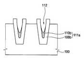
다음에, 상기 패드 산화막 패턴(102)을 습식 식각 공정을 통해 완전히 제거함으로서 액티브 영역에 해당되는 기판(100)을 선택적으로 노출시킨다. 이 때, 상기 패드 산화막 패턴(102)을 제거하기 위한 공정 시간을 조절하여 상기 제1 절연막 패턴(108b) 및 제2 절연막 패턴(110b) 부분적으로 식각함으로서 중앙 부위에 제2 리세스(112)를 갖는 트렌치 소자 분리막(111a)을 완성한다. 상기 패드 산화막 패턴(102)을 제거하기 위한 식각액으로는 예를 들어 NH4F, HF 및 물의 혼합 용액인 LAL용액을 사용할 수 있다.Next, the pad
좀 더 상세하게 설명하면, 상기 패드 산화막 패턴(102)을 식각하기 위한 습 식 식각액을 유입하면, 상기 패드 산화막 패턴(102) 뿐 아니라 상기 제1 절연막 패턴(108b) 및 제2 절연막 패턴(110b)도 동시에 식각된다. 이 때, 상기 제2 절연막 패턴(110b)은 상기 제1 절연막 패턴(108b)에 비해 빠르게 식각되기 때문에 상기 제2 절연막 패턴(110b) 부위에 제2 리세스(112)가 생기게 된다. 상기 제2 리세스(112)의 저면이 적어도 상기 기판(100)의 상부 표면보다 낮게 위치하도록 상기 식각 조건을 조절하여야 한다. 상기 식각 공정에서 상기 제2 절연막 패턴(110b)이 완전히 제거될 수도 있고 상기 제2 절연막 패턴(110b)이 일부 남아있을 수도 있다.In more detail, when a wet etching solution for etching the
상기 설명한 공정에 의하면, 중앙 부위에 기판 표면 하부까지 연장되는 리세스를 갖는 트렌치 소자 분리막을 형성할 수 있다. 상기 트렌치 소자 분리막을 이용하는 경우, 상기 리세스 부위에 기생 커패시턴스를 감소시키기 위한 패턴을 삽입할 수 있으므로 기생 커패시턴스를 감소시키기에 적합하다.According to the above-described process, it is possible to form a trench element isolation film having a recess extending to the lower portion of the substrate surface in the central portion. In the case of using the trench isolation layer, a pattern for reducing parasitic capacitance may be inserted into the recess, thereby reducing the parasitic capacitance.
제2 실시예Second embodiment
도 7 내지 도 12는 본 발명의 제2 실시예에 따른 불휘발성 메모리 장치의 제조 방법을 설명하기 위한 단면도들이다. 이하에서 설명하는 불휘발성 메모리 장치의 제조 방법에서, 트렌치 소자 분리막 형성 방법은 상기 제1 실시예의 방법과 매우 유사하다.7 through 12 are cross-sectional views illustrating a method of manufacturing a nonvolatile memory device in accordance with a second embodiment of the present invention. In the method of manufacturing a nonvolatile memory device described below, the trench element isolation film forming method is very similar to the method of the first embodiment.
도 7을 참조하면, 도 2 내지 도 4에서 설명한 것과 동일한 공정을 수행한다. 간단히 설명하면, 기판(150)에 패드 산화막(도시안됨) 및 실리콘 질화막(도시안됨)을 형성한다. 상기 패드 산화막은 실리콘 질화막을 형성할 시에 발생하는 스트레스 를 감소시키기 위해 구비된다. 상기 실리콘 질화막은 소자 분리용 트렌치를 형성하기 위한 마스크로도 사용될 뿐 아니라 플로팅 게이트가 형성될 부위를 정의하기 위한 막으로도 제공된다. 때문에, 상기 실리콘 질화막은 형성하고자 하는 플로팅 게이트의 두께보다는 더 두껍게 형성하여야 한다.Referring to FIG. 7, the same process as described with reference to FIGS. 2 to 4 is performed. In brief, a pad oxide film (not shown) and a silicon nitride film (not shown) are formed on the
이어서, 상기 실리콘 질화막 및 패드 산화막을 부분적으로 식각하여 패드 산화막 패턴(152) 및 실리콘 질화막 패턴(154)이 적층된 형태의 하드 마스크 패턴(155)을 형성한다. 상기 하드 마스크 패턴(155)을 식각 마스크로 이용하여 상기 기판(150)을 식각함으로서, 상기 기판(150)에 소자 분리용 트렌치(156)를 형성한다.Subsequently, the silicon nitride film and the pad oxide film are partially etched to form a
다음에, 도 7에 도시된 것과 같이, 상기 소자 분리용 트렌치(156) 내부 및 상기 하드 마스크 패턴 표면(155)상에 상기 소자 분리용 트렌치 내부를 부분적으로 매립하는 제1 절연막(158)을 형성한다. 상기 제1 절연막(158)은 상기 소자 분리용 트렌치(156) 내부에 제1 리세스(159)를 갖는다. 상기 제1 절연막(158)은 실리콘 산화물로 형성될 수 있다.Next, as shown in FIG. 7, a first insulating
이 때, 상기 제1 리세스(159)의 저면은 기판 상부 표면보다 더 아래에 위치하도록 형성되어야 한다. 상기 제1 절연막(158)은 감압(sub-atmosphere), 저압 또는 상압 화학 기상 증착 방법을 이용하여 형성할 수 있다.At this time, the bottom of the
구체적으로, 상기 제1 절연막(158)을 형성하기 위한 소오스의 예로서는 TEOS를 들 수 있으며, 반응 가스로는 오존, 산소 및 N2O 가스를 예로 들 수 있다. 상기 반응 가스는 단독 또는 혼합하여 사용할 수 있다.Specifically, examples of the source for forming the first insulating
상기 제1 절연막(158)을 형성하기 위한 소오스 가스의 다른 예로서는 SiH4를 들 수 있으며, 반응 가스로는 오존, 산소 및 N2O 가스를 예로 들 수 있다. 상기 반응 가스는 단독 또는 혼합하여 사용할 수 있다.Another example of the source gas for forming the first insulating
상기 제1 절연막(158)을 형성한 이 후에, 상기 제1 절연막(158)을 열처리할 수 있다. 상기 열처리의 온도 및 분위기를 조절함으로서 상기 제1 절연막(158)의 습식 식각율을 조절할 수 있다.After the first insulating
상기 제1 절연막(158) 상에 동일한 식각 조건에서 상기 제1 절연막(158)에 비해 식각율이 높은 특성을 갖는 예비 제2 절연막(도시안됨)을 증착한다. 상기 예비 제2 절연막은 상기 제1 리세스(159) 부위를 완전히 매립하도록 형성되어야 한다. 상기 예비 제2 절연막은 상기 소자 분리 트렌치(156) 폭보다 더 좁은 폭의 제1 리세스(159) 부위를 매립할 수 있도록 갭필 특성이 양호한 SOG법에 의해 형성될 수 있다. 예를 들어, 상기 예비 제2 절연막은 실라잔 계열의 물질 또는 유동성 산화물(FOX, Flowable oxide)를 코팅함으로서 형성할 수 있다.A preliminary second insulating layer (not shown) having a higher etching rate than the first insulating
다음에, 상기 예비 제2 절연막을 열처리함으로서 동일한 식각 조건에서 상부의 식각율이 하부의 식각율에 비해 상대적으로 낮은 제2 절연막(202)을 형성한다. 바람직하게는, 상기 제2 절연막(202)에서 하드 마스크 패턴(155)의 상부 표면 아래에 위치하는 부분(201)은 상기 하드 마스크 패턴(155) 상부 표면 위에 위치하는 부분에 비해 식각율이 상대적으로 낮게 형성되어야 한다. 상기 열처리의 온도 및 분위기를 조절함으로서 상기 제2 절연막(202)의 습식 식각율을 조절할 수 있다. 즉, 상기 열처리 온도가 상승할수록 상기 막의 밀도가 높아지게 되어 습식 식각율이 더 낮아지게 된다.Next, the second
구체적으로, 실라잔 계열의 물질 또는 유동성 산화물(FOX, Flowable oxide)를 코팅한 이 후에 공기 또는 질소 분위기의 200 내지 300℃ 온도하에서 1차 열처리한다. 상기 1차 열처리 후에, 분당 100℃ 이상의 램핑 스피드(ranping speed)로서 온도를 600 내지 800℃로 상승시킨다. 열처리 챔버 내의 온도가 600 내지 800℃ 범위 내의 설정 온도가 유지되면, 산소 또는 수증기 분위기에서 2차 열처리 한다. 상기 2차 열처리 후에, 분당 100℃ 이상의 램핑 스피드로서 온도를 900 내지 1000℃로 상승시킨다. 열처리 챔버 내의 온도가 900 내지 1000℃범위 내의 설정 온도가 유지되면, 아르곤 또는 질소 분위기에서 3차 열처리 한다.Specifically, after coating the silazane-based material or flowable oxide (FOX), the first heat treatment is carried out at 200 to 300 ℃ temperature of air or nitrogen atmosphere. After the first heat treatment, the temperature is raised to 600-800 ° C. with a ramping speed of 100 ° C. or more per minute. When the temperature in the heat treatment chamber is maintained at a set temperature in the range of 600 to 800 ° C., the second heat treatment is performed in an oxygen or water vapor atmosphere. After the secondary heat treatment, the temperature is raised to 900-1000 ° C. with a ramping speed of 100 ° C. or more per minute. When the temperature in the heat treatment chamber is maintained at a predetermined temperature in the range of 900 to 1000 ° C., the third heat treatment is performed in an argon or nitrogen atmosphere.
상기와 같이, 램핑 스피드를 분당 100℃ 이상으로 급속하게 상승시켜 열처리 공정을 수행하는 경우 상기 예비 제2 절연막의 상부는 충분히 열처리되어 막의 밀도가 증가하게 되고 상기 예비 제2 절연막의 하부는 충분히 열처리되지 못하여 막이 치밀하지 못하게 된다. 이 때, 막이 상대적으로 치밀하지 못한 부분은 습식 식각액에 의해 빠르게 식각된다. 그러므로, 상기 열처리에 의해 형성된 제2 절연막(202)의 상부(201)는 하부(200)에 비해 습식 식각율이 낮다.As described above, when the heat treatment process is performed by rapidly increasing the ramping speed to 100 ° C. or more per minute, the upper portion of the preliminary second insulating film is sufficiently heat treated to increase the density of the film, and the lower portion of the preliminary second insulating film is not sufficiently heat treated. The film is not dense. At this time, the portion where the membrane is not relatively dense is quickly etched by the wet etchant. Therefore, the
이하에서, 열처리 시의 램핑 스피드에 따른 막의 습식 식각율을 비교 실험한 결과를 설명한다.Hereinafter, a result of comparing the wet etch rate of the film according to the ramping speed during heat treatment will be described.
도 13 및 도 14는 열처리의 램핑 스피드 차이에 따라 SOG 물질막의 상, 하부 식각율의 차이를 보여주는 단면 SEM 이미지이다.13 and 14 are cross-sectional SEM images showing differences in upper and lower etching rates of the SOG material film according to the ramping speed difference of the heat treatment.
도 13은 다음과 같은 과정에 의해 수득한 SEM 이미지이다.13 is an SEM image obtained by the following process.
트렌치(352)가 형성되어 있는 기판(350)에 SOG막(354)을 코팅하고 250℃의 질소 분위기에서 1차 열처리한 후 램핑 스피드를 분당 50℃ 이하로 느리게 하여 온도를 800℃로 상승시켜 산소(O2) 분위기에서 2차 열처리하였다. 그리고, 상기 기판에서 SOG막이 매립되어 있는 트렌치 부분이 노출되도록 상기 기판을 절단하고 습식 식각액을 사용하여 설정된 시간동안 식각하였다.The
도 14는 다음과 같은 과정에 의해 수득한 SEM 이미지이다.14 is an SEM image obtained by the following process.
트렌치(352a)가 형성되어 있는 기판(350a)에 SOG막(358)을 코팅하고 250℃의 질소 분위기에서 1차 열처리한 후 램핑 스피드를 분당 100℃ 이상으로 빠르게 하여 온도를 800℃로 상승시켜 산소(O2) 분위기에서 2차 열처리하였다. 그리고, 상기 기판에서 SOG막(358)이 매립되어 있는 트렌치 부분이 노출되도록 상기 기판을 절단하고 습식 식각액을 사용하여 설정된 시간동안 식각하였다.The
상기 도 14에서와 같이 램핑 스피드를 느리게 하는 경우에는 SOG막(354)은 거의 식각되지 않았음을 알 수 있다. 즉, 상기 SOG막(354)의 상부 및 하부에서의 습식 식각율이 거의 동일하다는 것을 알 수 있다.As shown in FIG. 14, when the ramping speed is decreased, the
또한, 상기 제2 실시예에서와 같이 램핑 스피드를 분당 100℃이상으로 열처리 하는 경우에는 도 19에서 보여지듯이 SOG막(358)의 상부(358a)는 거의 식각되지 않고 하부(358b)만이 선택적으로 식각되었음을 알 수 있다. 즉, 열처리 시의 램핑 스피드를 빠르게 조절함으로서 상부에 비해 하부의 식각율이 높은 SOG막(358)을 형성할 수 있음을 알 수 있다.In addition, when the ramping speed is heat treated at 100 ° C. or more as in the second embodiment, as shown in FIG. 19, the
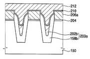
도 8을 참조하면, 상기 하드 마스크 패턴(155)의 표면이 노출되도록 화학 기계적으로 연마하여 소자 분리용 트렌치(156) 내부에만 제1 절연막 패턴(158a) 및 제2 절연막 패턴(202a)이 남아있는 예비 소자 분리막(203)을 형성한다.Referring to FIG. 8, the first insulating
상기 하드 마스크 패턴(155)의 상부 패턴인 실리콘 질화막 패턴(154)을 먼저 제거한다. 상기 실리콘 질화막 패턴(154)은 인산(H3PO4)와 같은 습식 식각액에 의해 제거될 수 있다.The silicon
다음에, 상기 패드 산화막 패턴(152)을 습식 식각 공정을 통해 완전히 제거함으로서 액티브 영역에 해당되는 기판(150)을 선택적으로 노출시킨다. 상기 패드 산화막 패턴(152)은 LAL용액으로 제거할 수 있다. 이 때, 상기 제1 절연막 패턴(158a) 및 제2 절연막 패턴(202a)도 상기 패드 산화막 패턴(152)의 두께만큼 일부 식각된다. 그러나, 상기 제2 절연막 패턴(202a)의 상부는 열처리에 의해 낮은 습식 식각율을 갖기 때문에 상기 습식 식각 공정에 의해 과도하게 식각되지 않는다.Next, the pad
상기 공정을 수행하면, 소자 분리 영역에는 예비 소자 분리막(203)이 상기 기판(150)보다 높게 형성된다. 이 때, 상기 예비 소자 분리막(203)의 상부면은 적어도 형성하고자하는 플로팅 게이트보다 더 높게 위치하여야 한다.When the process is performed, the
도 9를 참조하면, 상기 노출된 기판(150) 상에 터널 산화막(204)을 형성한다. 상기 터널 산화막(204)은 실리콘 산화막으로 형성될 수 있으나, 불소 도핑된 실리콘 산화막, 탄소 도핑된 실리콘 산화막, 저유전율(low-k) 물질막 등으로도 형성될 수 있다.Referring to FIG. 9, a
상기 터널 산화막(204) 상에 상기 예비 소자 분리막(203) 사이의 갭을 매립하도록 폴리실리콘막(206)을 형성한다. 상기 폴리실리콘막(206)은 통상의 LP-CVD공정에 의해 형성될 수 있다.The
도 10을 참조하면, 상기 예비 소자 분리막(203)의 상부면이 노출되도록 상기 폴리실리콘막(206)을 화학 기계적으로 연마하여 노드 분리함으로서 플로팅 게이트 패턴(206a)을 형성한다.Referring to FIG. 10, a floating
도 11을 참조하면, 상기 플로팅 게이트 패턴(206a) 사이의 예비 소자 분리막(203)을 부분적으로 습식 식각하여 중앙 부위에 제2 리세스(208)를 갖는 트렌치 소자 분리막(203a)을 완성한다. 상기 예비 소자 분리막(203)은 LAL용액으로 제거할 수 있다.Referring to FIG. 11, the
구체적으로, 상기 습식 식각 공정을 수행하면 예비 소자 분리막(203)의 제1 절연막 패턴(158b) 및 제2 절연막 패턴(202b)이 유사한 속도로 제거된다. 그러나, 상기 제2 절연막 패턴(202b)이 일정 두께로 식각되어 하부의 식각율이 상대적으로 높은 부위에 도달하면 상기 제1 절연막 패턴(158b)에 비해 빠르게 식각이 이루어진다. 따라서, 상기 제2 절연막 패턴(202b)의 중심 부위에는 제2 리세스(208)가 생성된다. 이 때, 상기 습식 식각 공정을 수행할 때 도 11에서와 같이 상기 제2 절연막 패턴(202b)을 일부 남길 수도 있다. 그러나, 상기 제2 절연막 패턴(202b)을 모두 제거하여도 무방하다.In detail, when the wet etching process is performed, the first insulating layer pattern 158b and the second insulating
도 12를 참조하면, 상기 플로팅 게이트 패턴(206a) 및 트렌치 소자 분리막(203a)의 표면 상에 유전막(210)을 형성한다. 상기 유전막(210)은 산화막/질화막/산화막의 적층구조(이하, ONO막)로 형성될 수 있다. 또는, 상기 유전막(210)은 고유전 물질막으로도 형성될 수 있다.Referring to FIG. 12, a
상기 유전막(210)상에, 상기 제2 리세스(208) 부위를 매립하는 도전막(도시 안됨)을 형성한다. 상기 도전막은 폴리실리콘막으로 이루어질 수 있다. 또는, 상기 도전막은 폴리실리콘막/금속 실리사이드막 또는 폴리실리콘막/금속막의 적층 구조로 이루어질 수 있다. 상기 도전막을 패터닝하여 콘트롤 게이트(212)를 형성한다. 계속하여, 도시하지는 않았으나 상기 콘트롤 게이트가 형성됨에 따라 노출된 유전막 및 플로팅 게이트 패턴을 부분적으로 식각하여 플로팅 게이트를 완성한다.On the
이 때, 상기 콘트롤 게이트(212)은 상기 플로팅 게이트 사이에서 액티브 영역 아래까지 연장된 형상을 갖는다. 즉, 상기 콘트롤 게이트(212)는 상기 플로팅 게이트들이 서로 직접적으로 대향하지 않도록 방해하는 구조를 갖는다. 따라서, 인접한 플로팅 게이트들 간에서 발생되는 기생 커패시턴스가 감소된다.At this time, the
상기 공정에 의해 형성되는 불휘발성 메모리 장치는 인접한 플로팅 게이트 들 간에 발생되는 기생 커패시턴스가 감소되고 이로 인해 셀 산포가 개선된다. 그러므로, 특히 멀티 레벨 셀로 구동되는 불휘발성 메모리 장치에 적용하기에 매우 적합하다. 더구나, 상기 구성을 갖는 불휘발성 메모리 장치를 구현하기 위해 별도의 건식 식각 공정이 요구되지 않기 때문에 건식 식각 공정 시의 플라즈마 데미지의 영향을 받지 않는다. 때문에, 상기 불휘발성 메모리 장치의 동작 특성 향상 및 신뢰성 향상을 기대할 수 있다.In the nonvolatile memory device formed by the above process, parasitic capacitances generated between adjacent floating gates are reduced, thereby improving cell dispersion. Therefore, it is particularly well suited for application to nonvolatile memory devices driven by multi-level cells. In addition, since a separate dry etching process is not required to implement the nonvolatile memory device having the above-described configuration, plasma damage is not affected by the dry etching process. Therefore, it is expected to improve the operation characteristics and the reliability of the nonvolatile memory device.
제3 실시예Third embodiment
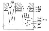
도 15 내지 도 19는 본 발명의 제3 실시예에 따른 불휘발성 메모리 장치의 제조 방법을 설명하기 위한 단면도들이다.15 to 19 are cross-sectional views illustrating a method of manufacturing a nonvolatile memory device in accordance with a third embodiment of the present invention.
도 15를 참조하면, 기판(300)상에 터널 산화막(도시안됨)을 형성한다. 상기 터널 산화막은 실리콘 산화막으로 형성될 수 있으나, 불소 도핑된 실리콘 산화막, 탄소 도핑된 실리콘 산화막, 저유전율(low-k) 물질막 등으로도 형성될 수 있다. 상기 터널 산화막 상에 하부 플로팅 게이트 패턴으로 제공되기 위한 제1 폴리실리콘막(도시안됨)을 형성한다. 상기 제1 폴리실리콘막 상에 하드 마스크막으로 제공되는 실리콘 질화막(도시안됨)을 형성한다.Referring to FIG. 15, a tunnel oxide film (not shown) is formed on the
상기 실리콘 질화막을 사진 식각 공정에 의해 패터닝하여 하드 마스크 패턴(306)을 형성한다. 다음에, 상기 하드 마스크 패턴(306)을 식각 마스크로 이용하여 상기 제1 폴리실리콘막 및 터널 산화막을 순차적으로 식각함으로서 터널 산화막 패턴(302) 및 하부 플로팅 게이트 패턴(304)을 형성한다. 계속적으로, 기판(300)을 식각함으로서 소자 분리용 트렌치(307)를 형성한다.The silicon nitride layer is patterned by a photolithography process to form a
다음에, 상기 소자 분리용 트렌치(307) 및 하드 마스크 패턴(306) 표면 상에 상기 소자 분리용 트렌치(307)를 부분적으로 매립하는 제1 절연막(308)을 증착한다. 상기 제1 절연막(308)은 상기 트렌치 내부에서 제1 리세스(309)를 갖는다. 상기 제1 절연막(308)은 실리콘 산화물로 형성될 수 있다. 이 때, 상기 제1 리세스(309) 저면은 기판(300) 상부면보다 더 아래에 위치하도록 형성되어야 한다. 상기 제1 절연막(308)은 감압(sub-atmosphere), 저압 또는 상압 화학 기상 증착 방법을 이용하여 형성할 수 있다. 상기 제1 절연막(308)을 형성하는 공정은 실시예 2와 동일하다.Next, a first insulating
도 16을 참조하면, 상기 제1 절연막(308) 상에 동일한 식각 조건에서 상기 제1 절연막(308)에 비해 식각율이 높은 특성을 갖는 제2 절연막(도시안됨)을 증착한다. 상기 제2 절연막은 상기 제1 리세스(309) 부위를 완전히 매립하도록 형성되어야 한다. 상기 제2 절연막은 상기 소자 분리용 트렌치(307) 폭보다 더 좁은 폭의 제1 리세스(309) 부위를 매립할 수 있도록 갭필 특성이 양호한 SOG법에 의해 형성될 수 있다. 예를 들어, 상기 제2 절연막은 실라잔 계열의 물질 또는 유동성 산화물(FOX, Flowable oxide)를 코팅함으로서 형성할 수 있다.Referring to FIG. 16, a second insulating layer (not shown) having a higher etching rate than the first insulating
상기 제2 절연막을 형성한 이 후에, 상기 제2 절연막을 열처리한다. 상기 열처리의 온도 및 분위기를 조절함으로서 상기 제2 절연막의 습식 식각율을 조절할 수 있다. 즉, 상기 열처리 온도가 상승할수록 상기 막의 밀도가 높아지게 되어 습식 식각율이 더 낮아지게 된다.After forming the second insulating film, the second insulating film is heat-treated. The wet etch rate of the second insulating layer may be controlled by controlling the temperature and the atmosphere of the heat treatment. That is, as the heat treatment temperature increases, the density of the film increases, and the wet etch rate is lowered.
본 실시예에서는 패드 산화막 형성 및 제거 공정이 수행되지 않고 플로팅 게이트 패턴이 화학 기계적 연마 공정에 의해 형성되지 않으므로 상기 제2 절연막의 상,하부 습식 식각율이 동일하여도 무방하다. 따라서, 상기 제2 절연막을 열처리할 시에 램핑 스피드가 실시예2에서와 같이 제한되지는 않는다.In this embodiment, since the pad oxide film forming and removing process is not performed and the floating gate pattern is not formed by the chemical mechanical polishing process, the upper and lower wet etching rates of the second insulating film may be the same. Therefore, the ramping speed is not limited as in Example 2 when heat-treating the second insulating film.
상기 SOG방법으로 형성된 상기 제2 절연막은 화학 기상 증착 방법에 의해 형성된 제1 절연막에 비해 막이 치밀하지 않다. 때문에, 동일한 습식 식각 조건에서 상기 제2 절연막은 상기 제1 절연막에 비해 빠르게 식각되는 특성을 갖는다.The second insulating film formed by the SOG method is less dense than the first insulating film formed by the chemical vapor deposition method. Therefore, in the same wet etching condition, the second insulating film has a characteristic of being etched faster than the first insulating film.
다음에, 상기 하드 마스크 패턴(306)의 표면이 노출되도록 화학 기계적으로 연마하여 소자 분리용 트렌치 내부에만 제1 절연막 패턴(308a) 및 제2 절연막 패턴(310a)이 남아있는 예비 소자 분리막(311)을 형성한다.Next, the preliminary
도 17을 참조하면, 상기 하드 마스크 패턴(306)을 인산(H3PO4)와 같은 습식 식각액을 사용하여 제거한다. 상기 하드 마스크 패턴(306)을 제거하면 표면에 하부 플로팅 게이트 패턴(304)이 노출된다.Referring to FIG. 17, the
상기 하부 플로팅 게이트 패턴(304) 및 예비 소자 분리막(311)의 상부면에 상부 플로팅 게이트로 제공되기 위한 제2 폴리실리콘막(도시안됨)을 형성한다. 상기 제2 폴리실리콘막을 부분적으로 식각함으로서 상기 하부 플로팅 게이트 패턴(304) 상에 상부 플로팅 게이트 패턴(312)을 형성한다. 상기 상부 플로팅 게이트 패턴(312)의 사이에는 상기 예비 소자 분리막(311)이 노출되어 있다.A second polysilicon layer (not shown) is formed on an upper surface of the lower floating
도 18을 참조하면, 상기 상,하부 플로팅 게이트 패턴(304, 312) 사이의 예비 소자 분리막(311)을 부분적으로 습식 식각하여 중앙 부위에 제2 리세스(313)를 갖는 트렌치 소자 분리막(311a)을 완성한다. 상기 예비 소자 분리막(311)은 LAL용액으로 제거할 수 있다.Referring to FIG. 18, a trench
구체적으로, 상기 습식 식각 공정을 수행하면 예비 소자 분리막(311)의 제1 절연막 패턴(308b)에 비해 상기 제2 절연막 패턴(310b)이 빠르게 식각된다. 따라서, 상기 제2 절연막 패턴(310b)의 중심 부위에는 제2 리세스(313)가 생성된다. 이 때, 상기 습식 식각 공정을 수행할 때 도 18에서와 같이 상기 제2 절연막 패턴(310b)을 일부 남길 수도 있다. 그러나, 상기 제2 절연막 패턴(310b)을 모두 제거하여도 무방하다.Specifically, when the wet etching process is performed, the second insulating
도 19를 참조하면, 상기 노출된 상부 플로팅 게이트 패턴(312) 및 소자 분리막(311a)의 표면상에 유전막(314)을 형성한다. 상기 유전막(314)은 산화막/질화막/ 산화막의 적층구조(이하, ONO막)로 형성될 수 있다. 또는, 상기 유전막(314)은 고유전 물질막으로도 형성될 수 있다.Referring to FIG. 19, a
상기 유전막(314) 상에, 상기 제2 리세스(313) 부위를 매립하는 도전막(도시안됨)을 형성한다. 상기 도전막은 폴리실리콘막으로 이루어질 수 있다. 또는, 상기 도전막은 폴리실리콘막/금속 실리사이드막 또는 폴리실리콘막/금속막의 적층 구조로 이루어질 수 있다. 상기 도전막을 패터닝함으로서 콘트롤 게이트(316)를 형성한다. 상기 콘트롤 게이트는 상기 플로팅 게이트 패턴 사이에서 액티브 영역 아래까지 연장된 형상을 갖는다.A conductive film (not shown) is formed on the
계속하여, 도시하지는 않았으나 상기 콘트롤 게이트(316)가 형성됨에 따라 노출된 유전막 및 상부, 하부 플로팅 게이트 패턴을 부분적으로 식각하여 플로팅 게이트를 완성한다.Subsequently, although not shown, as the
상술한 바와 같이 본 발명에 의하면, 플라즈마를 이용하는 건식 식각 공정을 수행하지 않고도 소자 분리막의 중심 부위에 리세스를 형성할 수 있다. 또한, 상기 리세스 부위에 콘트롤 게이트용 도전물질을 증착시킴으로서, 상기 플로팅 게이트와의 기생 커패시턴스를 감소시킬 수 있다. 때문에, 상기 리세스 형성시에 표면 데미지 발생을 최소화할 수 있어 반도체 장치의 특성을 향상시킬 수 있다.As described above, according to the present invention, a recess may be formed in a central portion of the device isolation layer without performing a dry etching process using plasma. In addition, by depositing a conductive material for the control gate on the recess, parasitic capacitance with the floating gate may be reduced. Therefore, the occurrence of surface damage at the time of forming the recess can be minimized, thereby improving the characteristics of the semiconductor device.
상술한 바와 같이, 본 발명의 바람직한 실시예를 참조하여 설명하였지만 해당 기술 분야의 숙련된 당업자라면 하기의 특허 청구의 범위에 기재된 본 발명의 사상 및 영역으로부터 벗어나지 않는 범위 내에서 본 발명을 다양하게 수정 및 변 경시킬 수 있음을 이해할 수 있을 것이다.As described above, although described with reference to a preferred embodiment of the present invention, those skilled in the art will be variously modified without departing from the spirit and scope of the invention described in the claims below. And can be changed.
Claims (23)
Translated fromKoreanPriority Applications (2)
| Application Number | Priority Date | Filing Date | Title |
|---|---|---|---|
| KR1020040089213AKR100556527B1 (en) | 2004-11-04 | 2004-11-04 | Trench isolation layer formation method and nonvolatile memory device manufacturing method |
| US11/267,360US7601588B2 (en) | 2004-11-04 | 2005-11-04 | Method of forming a trench isolation layer and method of manufacturing a non-volatile memory device using the same |
Applications Claiming Priority (1)
| Application Number | Priority Date | Filing Date | Title |
|---|---|---|---|
| KR1020040089213AKR100556527B1 (en) | 2004-11-04 | 2004-11-04 | Trench isolation layer formation method and nonvolatile memory device manufacturing method |
Publications (1)
| Publication Number | Publication Date |
|---|---|
| KR100556527B1true KR100556527B1 (en) | 2006-03-06 |
Family
ID=36262571
Family Applications (1)
| Application Number | Title | Priority Date | Filing Date |
|---|---|---|---|
| KR1020040089213AExpired - Fee RelatedKR100556527B1 (en) | 2004-11-04 | 2004-11-04 | Trench isolation layer formation method and nonvolatile memory device manufacturing method |
Country Status (2)
| Country | Link |
|---|---|
| US (1) | US7601588B2 (en) |
| KR (1) | KR100556527B1 (en) |
Cited By (6)
| Publication number | Priority date | Publication date | Assignee | Title |
|---|---|---|---|---|
| KR100822606B1 (en)* | 2006-12-28 | 2008-04-16 | 주식회사 하이닉스반도체 | Device Separation Method of Semiconductor Memory Device |
| KR100880341B1 (en) | 2007-06-27 | 2009-01-28 | 주식회사 하이닉스반도체 | Device Separating Method of Flash Memory Device |
| KR100880342B1 (en) | 2007-06-27 | 2009-01-28 | 주식회사 하이닉스반도체 | Device Separator Formation Method of Semiconductor Device |
| KR100894772B1 (en)* | 2007-09-05 | 2009-04-24 | 주식회사 하이닉스반도체 | Semiconductor memory device and manufacturing method thereof |
| KR100922989B1 (en)* | 2007-04-25 | 2009-10-22 | 주식회사 하이닉스반도체 | Flash memory device and method of manufacturing thereof |
| KR100946116B1 (en) | 2007-06-27 | 2010-03-10 | 주식회사 하이닉스반도체 | Device Separating Method of Flash Memory Device |
Families Citing this family (20)
| Publication number | Priority date | Publication date | Assignee | Title |
|---|---|---|---|---|
| KR100685730B1 (en)* | 2005-05-02 | 2007-02-26 | 삼성전자주식회사 | Method of forming insulating film structure and method of manufacturing semiconductor device using same |
| US7811935B2 (en)* | 2006-03-07 | 2010-10-12 | Micron Technology, Inc. | Isolation regions and their formation |
| US7998809B2 (en)* | 2006-05-15 | 2011-08-16 | Micron Technology, Inc. | Method for forming a floating gate using chemical mechanical planarization |
| KR100780643B1 (en) | 2006-06-29 | 2007-11-29 | 주식회사 하이닉스반도체 | Device Separator Formation Method of Semiconductor Device |
| US7968425B2 (en)* | 2006-07-14 | 2011-06-28 | Micron Technology, Inc. | Isolation regions |
| KR100790296B1 (en)* | 2006-12-04 | 2008-01-02 | 주식회사 하이닉스반도체 | Manufacturing Method of Flash Memory Device |
| KR100972881B1 (en)* | 2007-06-28 | 2010-07-28 | 주식회사 하이닉스반도체 | How to Form a Flash Memory Device |
| KR100937818B1 (en)* | 2007-08-20 | 2010-01-20 | 주식회사 하이닉스반도체 | Flash memory device and manufacturing method thereof |
| KR101394553B1 (en)* | 2007-11-08 | 2014-05-14 | 삼성전자주식회사 | Nonvolatile memory device and method of forming the same |
| KR101402890B1 (en)* | 2007-11-30 | 2014-06-27 | 삼성전자주식회사 | Nonvolatile memory device and method for forming the same |
| KR101026382B1 (en)* | 2007-12-28 | 2011-04-07 | 주식회사 하이닉스반도체 | Device Separating Method of Semiconductor Device |
| KR101642157B1 (en)* | 2008-03-14 | 2016-07-22 | 스티븐 존 랄프 | Mitochondrially delivered anti-cancer compounds |
| KR20110003191A (en)* | 2009-07-03 | 2011-01-11 | 삼성전자주식회사 | Device Separation and Method of Forming Semiconductor Device |
| DE102010039298B4 (en)* | 2010-08-13 | 2022-11-10 | Robert Bosch Gmbh | Process for filling cavities in wafers |
| JP2012231007A (en)* | 2011-04-26 | 2012-11-22 | Elpida Memory Inc | Method of manufacturing semiconductor device |
| US20150295033A1 (en)* | 2012-11-30 | 2015-10-15 | Ps5 Luxco S.A.R.L. | Apparatus and method for manufacturing same |
| US9960074B2 (en)* | 2016-06-30 | 2018-05-01 | Taiwan Semiconductor Manufacturing Company, Ltd. | Integrated bi-layer STI deposition |
| US20190198630A1 (en)* | 2017-12-21 | 2019-06-27 | Macronix International Co., Ltd. | Managing Gate Coupling For Memory Devices |
| US10304680B1 (en) | 2017-12-22 | 2019-05-28 | Macronix International Co., Ltd. | Fabricating semiconductor devices having patterns with different feature sizes |
| TWI706452B (en)* | 2019-04-11 | 2020-10-01 | 台灣茂矽電子股份有限公司 | Manufacturing method of gate structure and gate structure |
Citations (4)
| Publication number | Priority date | Publication date | Assignee | Title |
|---|---|---|---|---|
| KR20010063307A (en)* | 1999-12-22 | 2001-07-09 | 박종섭 | Method for forming isolation layer of semiconductor device |
| KR20040053441A (en)* | 2002-12-14 | 2004-06-24 | 주식회사 하이닉스반도체 | Method of manufacturing a flash memory device |
| KR20040058798A (en)* | 2002-12-27 | 2004-07-05 | 주식회사 하이닉스반도체 | Method for forming device isolation film of semiconductor device |
| KR20040069769A (en)* | 2003-01-30 | 2004-08-06 | 아남반도체 주식회사 | Manufacturing method of semiconductor device |
Family Cites Families (5)
| Publication number | Priority date | Publication date | Assignee | Title |
|---|---|---|---|---|
| US6159801A (en)* | 1999-04-26 | 2000-12-12 | Taiwan Semiconductor Manufacturing Company | Method to increase coupling ratio of source to floating gate in split-gate flash |
| US20020081817A1 (en)* | 2000-12-22 | 2002-06-27 | Jayendra Bhakta | Void reduction and increased throughput in trench fill processes |
| KR100598092B1 (en) | 2001-05-18 | 2006-07-07 | 삼성전자주식회사 | Flash memory and its formation method |
| JP2003031650A (en) | 2001-07-13 | 2003-01-31 | Toshiba Corp | Method for manufacturing semiconductor device |
| JP2005332885A (en)* | 2004-05-18 | 2005-12-02 | Toshiba Corp | Nonvolatile semiconductor memory device and manufacturing method thereof |
- 2004
- 2004-11-04KRKR1020040089213Apatent/KR100556527B1/ennot_activeExpired - Fee Related
- 2005
- 2005-11-04USUS11/267,360patent/US7601588B2/ennot_activeExpired - Fee Related
Patent Citations (4)
| Publication number | Priority date | Publication date | Assignee | Title |
|---|---|---|---|---|
| KR20010063307A (en)* | 1999-12-22 | 2001-07-09 | 박종섭 | Method for forming isolation layer of semiconductor device |
| KR20040053441A (en)* | 2002-12-14 | 2004-06-24 | 주식회사 하이닉스반도체 | Method of manufacturing a flash memory device |
| KR20040058798A (en)* | 2002-12-27 | 2004-07-05 | 주식회사 하이닉스반도체 | Method for forming device isolation film of semiconductor device |
| KR20040069769A (en)* | 2003-01-30 | 2004-08-06 | 아남반도체 주식회사 | Manufacturing method of semiconductor device |
Cited By (7)
| Publication number | Priority date | Publication date | Assignee | Title |
|---|---|---|---|---|
| KR100822606B1 (en)* | 2006-12-28 | 2008-04-16 | 주식회사 하이닉스반도체 | Device Separation Method of Semiconductor Memory Device |
| KR100922989B1 (en)* | 2007-04-25 | 2009-10-22 | 주식회사 하이닉스반도체 | Flash memory device and method of manufacturing thereof |
| KR100880341B1 (en) | 2007-06-27 | 2009-01-28 | 주식회사 하이닉스반도체 | Device Separating Method of Flash Memory Device |
| KR100880342B1 (en) | 2007-06-27 | 2009-01-28 | 주식회사 하이닉스반도체 | Device Separator Formation Method of Semiconductor Device |
| KR100946116B1 (en) | 2007-06-27 | 2010-03-10 | 주식회사 하이닉스반도체 | Device Separating Method of Flash Memory Device |
| US8163627B2 (en) | 2007-06-27 | 2012-04-24 | Hynix Semiconductor Inc. | Method of forming isolation layer of semiconductor device |
| KR100894772B1 (en)* | 2007-09-05 | 2009-04-24 | 주식회사 하이닉스반도체 | Semiconductor memory device and manufacturing method thereof |
Also Published As
| Publication number | Publication date |
|---|---|
| US7601588B2 (en) | 2009-10-13 |
| US20060094203A1 (en) | 2006-05-04 |
Similar Documents
| Publication | Publication Date | Title |
|---|---|---|
| KR100556527B1 (en) | Trench isolation layer formation method and nonvolatile memory device manufacturing method | |
| US6117733A (en) | Poly tip formation and self-align source process for split-gate flash cell | |
| US7566929B2 (en) | Nonvolatile memory devices having floating gate electrodes with nitrogen-doped layers on portions thereof | |
| US6380035B1 (en) | Poly tip formation and self-align source process for split-gate flash cell | |
| KR100554516B1 (en) | Manufacturing Method of Semiconductor Device | |
| JP2004281662A (en) | Semiconductor storage device and method of manufacturing the same | |
| KR20080031076A (en) | Manufacturing method of nonvolatile memory device | |
| JP4282692B2 (en) | Manufacturing method of semiconductor device | |
| KR100397176B1 (en) | Method of planarizing non-volatile memory device | |
| US7807580B2 (en) | Triple poly-si replacement scheme for memory devices | |
| JP2003197789A (en) | Method for forming self-aligned floating gate of flash memory cell | |
| KR100552588B1 (en) | Manufacturing Method of Semiconductor Device | |
| KR100956599B1 (en) | Manufacturing method of nonvolatile memory device | |
| US6969653B2 (en) | Methods of manufacturing and-type flash memory devices | |
| JP2005311279A (en) | Method for manufacturing flash memory element and flash memory element manufactured by it | |
| KR100649974B1 (en) | Flash memory device having recessed floating gate and manufacturing method thereof | |
| JP2001057394A (en) | Nonvolatile semiconductor memory device and method of manufacturing the same | |
| JP5313547B2 (en) | Manufacturing method of semiconductor device | |
| KR100801062B1 (en) | Trench isolation method, gate structure formation method and nonvolatile memory device formation method | |
| US20090142914A1 (en) | Method for Manufacturing Semiconductor Device | |
| KR100880341B1 (en) | Device Separating Method of Flash Memory Device | |
| KR20020079380A (en) | Non-volatile semiconductor memory device and method for producing the same | |
| US20080242047A1 (en) | Method of forming isolation structure of semiconductor memory device | |
| US20090170263A1 (en) | Method of manufacturing flash memory device | |
| JP2010040754A (en) | Semiconductor device and method of manufacturing the same |
Legal Events
| Date | Code | Title | Description |
|---|---|---|---|
| A201 | Request for examination | ||
| PA0109 | Patent application | St.27 status event code:A-0-1-A10-A12-nap-PA0109 | |
| PA0201 | Request for examination | St.27 status event code:A-1-2-D10-D11-exm-PA0201 | |
| PN2301 | Change of applicant | St.27 status event code:A-3-3-R10-R13-asn-PN2301 St.27 status event code:A-3-3-R10-R11-asn-PN2301 | |
| PN2301 | Change of applicant | St.27 status event code:A-3-3-R10-R13-asn-PN2301 St.27 status event code:A-3-3-R10-R11-asn-PN2301 | |
| D13-X000 | Search requested | St.27 status event code:A-1-2-D10-D13-srh-X000 | |
| D14-X000 | Search report completed | St.27 status event code:A-1-2-D10-D14-srh-X000 | |
| E701 | Decision to grant or registration of patent right | ||
| PE0701 | Decision of registration | St.27 status event code:A-1-2-D10-D22-exm-PE0701 | |
| GRNT | Written decision to grant | ||
| PR0701 | Registration of establishment | St.27 status event code:A-2-4-F10-F11-exm-PR0701 | |
| PR1002 | Payment of registration fee | St.27 status event code:A-2-2-U10-U11-oth-PR1002 Fee payment year number:1 | |
| PG1601 | Publication of registration | St.27 status event code:A-4-4-Q10-Q13-nap-PG1601 | |
| PR1001 | Payment of annual fee | St.27 status event code:A-4-4-U10-U11-oth-PR1001 Fee payment year number:4 | |
| PR1001 | Payment of annual fee | St.27 status event code:A-4-4-U10-U11-oth-PR1001 Fee payment year number:5 | |
| PR1001 | Payment of annual fee | St.27 status event code:A-4-4-U10-U11-oth-PR1001 Fee payment year number:6 | |
| PR1001 | Payment of annual fee | St.27 status event code:A-4-4-U10-U11-oth-PR1001 Fee payment year number:7 | |
| R18-X000 | Changes to party contact information recorded | St.27 status event code:A-5-5-R10-R18-oth-X000 | |
| FPAY | Annual fee payment | Payment date:20130131 Year of fee payment:8 | |
| PR1001 | Payment of annual fee | St.27 status event code:A-4-4-U10-U11-oth-PR1001 Fee payment year number:8 | |
| FPAY | Annual fee payment | Payment date:20140129 Year of fee payment:9 | |
| PR1001 | Payment of annual fee | St.27 status event code:A-4-4-U10-U11-oth-PR1001 Fee payment year number:9 | |
| FPAY | Annual fee payment | Payment date:20150202 Year of fee payment:10 | |
| PR1001 | Payment of annual fee | St.27 status event code:A-4-4-U10-U11-oth-PR1001 Fee payment year number:10 | |
| PR1001 | Payment of annual fee | St.27 status event code:A-4-4-U10-U11-oth-PR1001 Fee payment year number:11 | |
| PR1001 | Payment of annual fee | St.27 status event code:A-4-4-U10-U11-oth-PR1001 Fee payment year number:12 | |
| PR1001 | Payment of annual fee | St.27 status event code:A-4-4-U10-U11-oth-PR1001 Fee payment year number:13 | |
| PR1001 | Payment of annual fee | St.27 status event code:A-4-4-U10-U11-oth-PR1001 Fee payment year number:14 | |
| FPAY | Annual fee payment | Payment date:20200131 Year of fee payment:15 | |
| PR1001 | Payment of annual fee | St.27 status event code:A-4-4-U10-U11-oth-PR1001 Fee payment year number:15 | |
| PR1001 | Payment of annual fee | St.27 status event code:A-4-4-U10-U11-oth-PR1001 Fee payment year number:16 | |
| PR1001 | Payment of annual fee | St.27 status event code:A-4-4-U10-U11-oth-PR1001 Fee payment year number:17 | |
| PR1001 | Payment of annual fee | St.27 status event code:A-4-4-U10-U11-oth-PR1001 Fee payment year number:18 | |
| PC1903 | Unpaid annual fee | St.27 status event code:A-4-4-U10-U13-oth-PC1903 Not in force date:20240224 Payment event data comment text:Termination Category : DEFAULT_OF_REGISTRATION_FEE | |
| P22-X000 | Classification modified | St.27 status event code:A-4-4-P10-P22-nap-X000 | |
| PC1903 | Unpaid annual fee | St.27 status event code:N-4-6-H10-H13-oth-PC1903 Ip right cessation event data comment text:Termination Category : DEFAULT_OF_REGISTRATION_FEE Not in force date:20240224 | |
| P22-X000 | Classification modified | St.27 status event code:A-4-4-P10-P22-nap-X000 |