KR100552975B1 - Active matrix organic light emitting display device and manufacturing method thereof - Google Patents
Active matrix organic light emitting display device and manufacturing method thereofDownload PDFInfo
- Publication number
- KR100552975B1 KR100552975B1KR1020030083391AKR20030083391AKR100552975B1KR 100552975 B1KR100552975 B1KR 100552975B1KR 1020030083391 AKR1020030083391 AKR 1020030083391AKR 20030083391 AKR20030083391 AKR 20030083391AKR 100552975 B1KR100552975 B1KR 100552975B1
- Authority
- KR
- South Korea
- Prior art keywords
- insulating film
- light emitting
- pixel electrode
- organic light
- via hole
- Prior art date
- Legal status (The legal status is an assumption and is not a legal conclusion. Google has not performed a legal analysis and makes no representation as to the accuracy of the status listed.)
- Expired - Fee Related
Links
Images


Classifications
- H—ELECTRICITY
- H05—ELECTRIC TECHNIQUES NOT OTHERWISE PROVIDED FOR
- H05B—ELECTRIC HEATING; ELECTRIC LIGHT SOURCES NOT OTHERWISE PROVIDED FOR; CIRCUIT ARRANGEMENTS FOR ELECTRIC LIGHT SOURCES, IN GENERAL
- H05B33/00—Electroluminescent light sources
- H—ELECTRICITY
- H10—SEMICONDUCTOR DEVICES; ELECTRIC SOLID-STATE DEVICES NOT OTHERWISE PROVIDED FOR
- H10K—ORGANIC ELECTRIC SOLID-STATE DEVICES
- H10K59/00—Integrated devices, or assemblies of multiple devices, comprising at least one organic light-emitting element covered by group H10K50/00
- H10K59/10—OLED displays
- H10K59/12—Active-matrix OLED [AMOLED] displays
- H10K59/122—Pixel-defining structures or layers, e.g. banks
- H—ELECTRICITY
- H10—SEMICONDUCTOR DEVICES; ELECTRIC SOLID-STATE DEVICES NOT OTHERWISE PROVIDED FOR
- H10K—ORGANIC ELECTRIC SOLID-STATE DEVICES
- H10K50/00—Organic light-emitting devices
- H10K50/80—Constructional details
- H10K50/805—Electrodes
- H10K50/81—Anodes
- H10K50/813—Anodes characterised by their shape
- H—ELECTRICITY
- H10—SEMICONDUCTOR DEVICES; ELECTRIC SOLID-STATE DEVICES NOT OTHERWISE PROVIDED FOR
- H10K—ORGANIC ELECTRIC SOLID-STATE DEVICES
- H10K59/00—Integrated devices, or assemblies of multiple devices, comprising at least one organic light-emitting element covered by group H10K50/00
- H10K59/10—OLED displays
- H10K59/12—Active-matrix OLED [AMOLED] displays
- H10K59/123—Connection of the pixel electrodes to the thin film transistors [TFT]
- H—ELECTRICITY
- H10—SEMICONDUCTOR DEVICES; ELECTRIC SOLID-STATE DEVICES NOT OTHERWISE PROVIDED FOR
- H10K—ORGANIC ELECTRIC SOLID-STATE DEVICES
- H10K59/00—Integrated devices, or assemblies of multiple devices, comprising at least one organic light-emitting element covered by group H10K50/00
- H10K59/10—OLED displays
- H10K59/12—Active-matrix OLED [AMOLED] displays
- H10K59/124—Insulating layers formed between TFT elements and OLED elements
- H—ELECTRICITY
- H10—SEMICONDUCTOR DEVICES; ELECTRIC SOLID-STATE DEVICES NOT OTHERWISE PROVIDED FOR
- H10K—ORGANIC ELECTRIC SOLID-STATE DEVICES
- H10K59/00—Integrated devices, or assemblies of multiple devices, comprising at least one organic light-emitting element covered by group H10K50/00
- H10K59/80—Constructional details
- H10K59/805—Electrodes
- H10K59/8051—Anodes
- H10K59/80515—Anodes characterised by their shape
Landscapes
- Engineering & Computer Science (AREA)
- Microelectronics & Electronic Packaging (AREA)
- Physics & Mathematics (AREA)
- Optics & Photonics (AREA)
- Electroluminescent Light Sources (AREA)
- Devices For Indicating Variable Information By Combining Individual Elements (AREA)
Abstract
Translated fromKoreanDescription
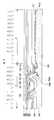
Translated fromKorean도 1은 종래의 능동 매트릭스 유기전계발광표시장치 및 그의 제조방법를 설명하기 위한 단면도이다.1 is a cross-sectional view illustrating a conventional active matrix organic light emitting display device and a method of manufacturing the same.
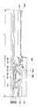
도 2a 내지 도 2c는 본 발명의 실시예에 따른 유기전계발광표시장치 및 그의 제조방법을 설명하기 위한 단면도들이다.2A to 2C are cross-sectional views illustrating an organic light emitting display device and a method of manufacturing the same according to an embodiment of the present invention.
(도면의 주요 부위에 대한 부호의 설명)(Explanation of symbols for main parts of drawing)
300 : 절연기판 365 : 비아홀300: insulating substrate 365: via hole
370 : 화소전극 377a : 제 1 감광성 유기절연막 패턴370:
377b : 제 2 감광성 유기절연막 패턴377b: second photosensitive organic insulating film pattern
본 발명은 유기전계발광표시장치 및 그의 제조방법에 관한 것으로, 특히 능동 매트릭스 유기전계발광표시장치 및 그의 제조방법에 관한 것이다.The present invention relates to an organic light emitting display device and a manufacturing method thereof, and more particularly, to an active matrix organic light emitting display device and a manufacturing method thereof.
일반적으로 유기전계발광표시장치(organic light emitting diode display)는 형광성 유기화합물을 전기적으로 여기시켜 발광하게 하는 자발광형 표시장치로서, 매트릭스 형태로 배치된 N×M 개의 화소들을 구동하는 방식에 따라 수동 매트릭스(passive matrix)방식과 능동 매트릭스(active matrix)방식으로 나뉘어지는데, 상기 능동 매트릭스 방식의 유기전계발광표시장치는 상기 수동 매트릭스 방식에 비해 전력소모가 적어 대면적 구현에 적합하며 고해상도를 갖는 장점이 있다.In general, an organic light emitting diode display is a self-luminous display that electrically excites a fluorescent organic compound to emit light. The organic light emitting diode display is passive according to a method of driving N × M pixels arranged in a matrix form. The matrix is divided into a passive matrix method and an active matrix method. The organic light emitting display device of the active matrix method has less power consumption than the passive matrix method, which is suitable for large area implementation and has a high resolution. have.
도 1은 종래의 능동 매트릭스 유기전계발광표시장치 및 그의 제조방법를 설명하기 위한 단면도이다.1 is a cross-sectional view illustrating a conventional active matrix organic light emitting display device and a method of manufacturing the same.
도 1을 참조하면, 절연기판(100) 상에 버퍼층(105)을 형성한다. 상기 절연기판(100)의 버퍼층(105) 상에 통상의 방법에 의해 활성층(110), 게이트 절연막(120) 게이트(130), 층간절연막(140) 및 소오스/드레인 전극(145)을 형성한다. 상기 소오스/드레인 전극(145)은 상기 층간절연막(140) 내에 형성된 콘택홀(141)에 의해 상기 활성층(110)과 접한다. 상기 활성층(110), 상기 게이트 절연막(120), 상기 게이트(130) 및 상기 소오스/드레인 전극(145)은 박막트랜지스터를 형성한다. 상기 박막트랜지스터를 포함하는 기판 전면에 걸쳐 패시베이션 절연막(150)을 형성하고, 상기 패시베이션 절연막(150) 내에 상기 소오스/드레인 전극들(145) 중 어느 하나를 노출시키는 비아홀(155)을 형성한다. 상기 패시베이션 절연막(150)은 무기막으로 평탄화특성이 불량하여 상기 패시베이션 절연막(150) 하부 패턴들 특히, 상기 콘택홀(141)의 토폴러지에 기인하는 골을 갖는다.Referring to FIG. 1, a
이어서, 상기 비아홀(155) 내에 노출된 소오스/드레인 전극(145)에 접하는 화소전극(170)을 형성한다. 이 때, 상기 화소전극(170)은 상기 비아홀(155)의 바닥 및 측벽을 따라 형성되므로, 상기 비아홀(155) 내에서 굴곡을 갖는 형태로 형성된 다. 이어서, 상기 비아홀(155) 내의 굴곡진 화소전극(170)을 덮는 화소정의막(175)을 형성하되, 상기 화소정의막(175)은 상기 비아홀(155)과 서로 이격된 위치에서 상기 화소전극(170)을 노출시키는 개구부(178)를 갖도록 형성한다. 이어서, 상기 개구부(178)내에 노출된 화소전극(170) 상에 유기발광층(180)을 형성하고, 상기 유기발광층(180) 상에 대향전극(opposite electrode; 190)을 형성한다. 상기 화소전극(170), 상기 유기발광층(180) 및 상기 대향전극(190)은 유기전계발광다이오드를 형성하고, 상기 유기전계발광다이오드는 상기 비아홀(155)을 통해 상기 박막트랜지스터에 연결됨으로써 상기 박막트랜지스터에 의해 구동된다.Subsequently, the
이러한 유기전계발광표시장치의 제조방법에 있어서, 상기 화소정의막(175)은 상기 유기발광층(180)이 상기 비아홀(150) 내의 상기 굴곡진 화소전극(170) 상에 위치하는 것을 막음으로써, 상기 유기발광층(180)의 굴곡으로 인한 열화를 막을 수 있다. 또한, 상기 하부패턴들 특히, 상기 콘택홀(141) 상부의 토폴러지를 완화시킴으로써, 상기 유기발광층(180)이 상기 콘택홀(141) 상부에서 굴곡되거나 끊어짐으로 인한 열화를 막을 수 있다.In the method of manufacturing the organic light emitting display device, the
한편, 상기 화소정의막(175)은 일반적으로 평탄화특성이 양호한 감광성 유기절연막를 사용하여 형성하는데, 상기 감광성 유기절연막은 감광제를 포함하고 있다. 유기전계발광표시장치의 구동에 있어, 상기 감광제는 아웃개스형태로 나와 상기 화소정의막(175)에 접하고 있는 상기 유기발광층(180)의 열화를 유발할 수 있다.On the other hand, the
본 발명이 이루고자 하는 기술적 과제는 상기한 종래기술의 문제점을 해결하기 위한 것으로, 감광성 유기절연막으로부터의 아웃개스에 의한 유기발광층의 열화를 최소화함과 동시에 상기 유기발광층의 굴곡으로 인한 열화를 방지할 수 있는 유기전계발광표시장치 및 그의 제조방법을 제공하고자 한다. The technical problem to be achieved by the present invention is to solve the problems of the prior art, it is possible to minimize the deterioration of the organic light emitting layer due to the outgas from the photosensitive organic insulating film and to prevent the deterioration due to the bending of the organic light emitting layer. An organic light emitting display device and a method of manufacturing the same are provided.
상기 기술적 과제를 이루기 위하여 본 발명은 유기전계발광표시장치를 제공한다. 상기 유기전계발광표시장치는 화소구동회로영역과 개구영역을 갖는 기판을 구비한다. 상기 기판의 화소구동회로영역 상에 소오스/드레인 전극을 갖는 박막트랜지스터가 위치한다. 상기 소오스/드레인 전극 상에 상기 소오스/드레인 전극을 노출시키는 비아홀을 갖는 패시베이션 절연막이 위치한다. 상기 비아홀의 바닥에 상기 노출된 소오스/드레인 전극에 접하는 화소전극이 위치하되, 상기 화소전극은 상기 패시베이션 절연막 상으로 연장된다. 상기 화소전극이 위치한 비아홀 내에 상기 비아홀을 메우고, 상기 비아홀 주변의 화소전극을 노출시키는 제 1 감광성 유기절연막 패턴이 위치한다. 상기 노출된 화소전극 상에 유기발광층이 위치한다.In order to achieve the above technical problem, the present invention provides an organic light emitting display device. The organic light emitting display device includes a substrate having a pixel driving circuit area and an opening area. A thin film transistor having a source / drain electrode is positioned on the pixel driver circuit area of the substrate. A passivation insulating layer having a via hole exposing the source / drain electrode is disposed on the source / drain electrode. A pixel electrode in contact with the exposed source / drain electrodes is positioned at the bottom of the via hole, and the pixel electrode extends over the passivation insulating layer. A first photosensitive organic insulating layer pattern is formed in the via hole in which the pixel electrode is positioned to expose the via hole and expose the pixel electrode around the via hole. An organic light emitting layer is positioned on the exposed pixel electrode.
바람직하게는 상기 제 1 감광성 유기절연막 패턴은 아크릴계 수지 또는 폴리이미드로 이루어진다.Preferably, the first photosensitive organic insulating film pattern is made of acrylic resin or polyimide.
바람직하게는 상기 패시베이션 절연막은 실리콘 질화막이다. 상기 패시베이션 절연막이 골을 갖는 경우, 상기 유기전계발광표시장치는 상기 패시베이션 절연막의 골을 메우는 제 2 감광성 유기절연막 패턴을 더욱 포함하는 것이 바람직하다. 바람직하게는 상기 제 2 감광성 유기절연막 패턴은 아크릴계 수지 또는 폴리이미드 로 이루어진다.Preferably, the passivation insulating film is a silicon nitride film. When the passivation insulating layer has a valley, the organic light emitting display device may further include a second photosensitive organic insulating layer pattern filling the valley of the passivation insulating layer. Preferably, the second photosensitive organic insulating film pattern is made of acrylic resin or polyimide.
바람직하게는 상기 화소전극은 ITO 또는 IZO로 이루어진다. 또한, 바람직하게는 상기 화소전극은 테이퍼진 에지를 갖는다. 더욱 바람직하게는 상기 화소전극의 테이퍼진 에지에 있어서, 상기 테이퍼는 20도 이하이다.Preferably, the pixel electrode is made of ITO or IZO. Also preferably, the pixel electrode has a tapered edge. More preferably, at the tapered edge of the pixel electrode, the taper is 20 degrees or less.
상기 기술적 과제를 이루기 위하여 본 발명은 유기전계발광표시장치의 제조방법을 제공한다. 상기 제조방법은 화소구동회로영역과 개구영역을 갖고, 상면과 하면을 갖는 기판을 제공하는 것을 포함한다. 상기 화소구동회로영역의 기판의 상면 상에 소오스/드레인 전극을 갖는 박막트랜지스터를 형성한다. 상기 소오스/드레인 전극을 포함한 기판의 상면 전체에 걸쳐 패시베이션 절연막을 형성한다. 상기 패시베이션 절연막 내에 상기 소오스/드레인 전극을 노출시키는 비아홀을 형성한다. 상기 비아홀의 바닥에 위치하여 상기 노출된 소오스/드레인 전극에 접하고, 상기 패시베이션 절연막 상으로 연장된 화소전극을 형성한다. 상기 화소전극을 포함한 기판의 상면 전체에 걸쳐 감광성 유기절연막을 형성한다. 상기 기판의 하면에서 광을 조사하여 상기 감광성 유기절연막을 백노광한다. 상기 노광된 감광성 유기전연막을 현상함으로써, 상기 개구영역의 화소전극을 노출시킨다. 상기 현상된 감광성 유기절연막을 에치백함으로써, 상기 비아홀을 메우는 제 1 감광성 유기절연막 패턴을 형성함과 동시에 상기 비아홀 주변의 화소전극을 노출시킨다. 상기 노출된 화소전극 상에 유기발광층을 형성한다.In order to achieve the above technical problem, the present invention provides a method of manufacturing an organic light emitting display device. The manufacturing method includes providing a substrate having a pixel driving circuit region and an opening region, the substrate having an upper surface and a lower surface. A thin film transistor having a source / drain electrode is formed on an upper surface of the substrate of the pixel driver circuit region. A passivation insulating film is formed over the entire upper surface of the substrate including the source / drain electrodes. A via hole exposing the source / drain electrode is formed in the passivation insulating layer. A pixel electrode is formed on the bottom of the via hole to contact the exposed source / drain electrode and extend on the passivation insulating layer. A photosensitive organic insulating film is formed over the entire upper surface of the substrate including the pixel electrode. The photosensitive organic insulating layer is exposed to white light by irradiating light from the lower surface of the substrate. By developing the exposed photosensitive organic conductive film, the pixel electrode of the opening region is exposed. By etching back the developed photosensitive organic insulating film, a first photosensitive organic insulating film pattern is formed to fill the via hole, and the pixel electrode around the via hole is exposed. An organic light emitting layer is formed on the exposed pixel electrode.
바람직하게는 상기 패시베이션 절연막은 실리콘 질화막으로 형성한다. 상기 패시베이션 절연막이 골을 갖는 경우, 상기 현상된 감광성 유기절연막을 에치백함 에 있어서, 상기 제 1 감광성 유기절연막 패턴을 형성함과 동시에 상기 패시베이션 절연막의 골을 메우는 제 2 감광성 유기절연막 패턴을 더욱 형성하는 것이 바람직하다.Preferably, the passivation insulating film is formed of a silicon nitride film. In the case where the passivation insulating film has a valley, in etching back the developed photosensitive organic insulating film, the first photosensitive organic insulating film pattern is formed and at the same time, a second photosensitive organic insulating film pattern filling the valley of the passivation insulating film is further formed. It is preferable.
바람직하게는 상기 화소전극은 ITO 또는 IZO로 형성한다. 또한, 바람직하게는 상기 화소전극은 테이퍼진 에지를 갖도록 형성한다. 더욱 바람직하게는 상기 화소전극을 테이퍼진 에지를 갖도록 형성함에 있어서, 상기 테이퍼는 20도 이하가 되도록 형성한다.Preferably, the pixel electrode is formed of ITO or IZO. Further, preferably, the pixel electrode is formed to have a tapered edge. More preferably, in forming the pixel electrode to have a tapered edge, the taper is formed to be 20 degrees or less.
바람직하게는 상기 감광성 유기절연막은 아크릴계 수지 또는 폴리이미드로 형성한다. 또한, 바람직하게는 상기 감광성 유기절연막은 스핀코팅을 사용하여 형성한다.Preferably, the photosensitive organic insulating film is formed of acrylic resin or polyimide. In addition, the photosensitive organic insulating layer is preferably formed using spin coating.
상기 에치백은 애슁을 사용하여 수행하는 것이 바람직하다.The etch back is preferably carried out using ashing.
이하, 본 발명을 보다 구체적으로 설명하기 위하여 본 발명에 따른 바람직한 실시예를 첨부된 도면을 참조하여 보다 상세하게 설명한다. 그러나, 본 발명은 여기서 설명되어지는 실시예에 한정되지 않고 다른 형태로 구체화될 수도 있다. 오히려 여기서 소개되는 실시예는 개시된 내용이 철저하고 완전해질 수 있도록 그리고 당업자에게 본 발명의 사상이 충분히 전달될 수 있도록 하기 위해 제공되어지는 것이다. 도면들에 있어서, 층이 다른 층 또는 기판 "상"에 있다고 언급되어지는 경우에 그것은 다른 층 또는 기판 상에 직접 형성될 수 있거나 또는 그들 사이에 제 3의 층이 개재될 수도 있다. 명세서 전체에 걸쳐서 동일한 참조번호들은 동일한 구성요소를 나타낸다.Hereinafter, exemplary embodiments of the present invention will be described in detail with reference to the accompanying drawings in order to describe the present invention in more detail. However, the present invention is not limited to the embodiments described herein but may be embodied in other forms. Rather, the embodiments introduced herein are provided so that the disclosure may be made thorough and complete, and to fully convey the spirit of the present invention to those skilled in the art. In the figures, where a layer is said to be "on" another layer or substrate, it may be formed directly on the other layer or substrate, or a third layer may be interposed therebetween. Like numbers refer to like elements throughout the specification.
도 2a 내지 도 2c는 본 발명의 실시예에 따른 유기전계발광표시장치 및 그의 제조방법을 설명하기 위한 단면도들이다. 상기 유기전계발광표시장치는 적어도 하나의 단위화소를 갖는데, 상기 단면도들은 상기 유기전계발광표시장치의 단위화소에 한정하여 나타낸 단면도들이다.2A to 2C are cross-sectional views illustrating an organic light emitting display device and a method of manufacturing the same according to an embodiment of the present invention. The organic light emitting display device has at least one unit pixel, and the cross-sectional views are cross-sectional views of a unit pixel of the organic light emitting display device.
도 2a를 참조하면, 개구영역(a) 및 화소구동회로영역(b)을 갖고 또한, 상면과 하면을 갖는 기판(300)을 제공한다. 상기 기판(300)은 투명한 기판으로 유리 또는 플라스틱으로 이루어진다. 상기 제공된 기판(300)의 상면 상에 버퍼층(305)을 형성한다. 상기 버퍼층(305)은 상기 기판(300)으로부터 유출되는 불순물로부터 후속하는 공정에서 형성되는 박막트랜지스터를 보호하기 위한 층으로, 실리콘 산화막, 실리콘 질화막 또는 이들이 적층된 이중층으로 형성할 수 있다.Referring to FIG. 2A, a
이어서, 상기 버퍼층(305)이 형성된 기판(300)의 상기 화소구동회로영역(b) 상에 활성층(310)을 형성한다. 상기 활성층(310)은 비정질 실리콘 또는 다결정 실리콘으로 형성할 수 있으나, 바람직하게는 다결정 실리콘으로 형성한다. 상기 활성층(310)을 포함한 기판 상면 전체에 걸쳐 게이트 절연막(320)을 형성하고, 상기 게이트 절연막(320) 상에 상기 활성층(310)의 소정영역에 대응되는 게이트(330)를 형성한다. 상기 게이트(330)을 마스크로 하여 상기 활성층(310)에 불순물을 주입함으로써, 상기 활성층에 소오스/드레인 영역들(315)을 형성함과 동시에 상기 소오스/드레인 영역들(315) 사이에 개재된 채널 영역(318)을 정의한다. 상기 게이트(330)를 포함한 기판 상면 전체에 걸쳐 층간 절연막(340)을 형성한다. 상기 층간 절연막(340)은 실리콘 산화막으로 형성할 수 있다. 이어서, 상기 층간 절연막(340) 내에 상기 소오스/드레인 영역들(315)을 각각 노출시키는 콘택홀들(341)을 형성한다. 상기 콘택홀들(341) 내에 노출된 상기 소오스/드레인 영역들(315) 및 상기 층간 절연막(340) 상에 금속막을 적층하고 이를 패터닝함으로써, 소오스/드레인 전극들(345)을 형성한다. 상기 활성층(310), 상기 게이트(330) 및 상기 소오스/드레인 전극들(345)은 박막트랜지스터를 구성한다.Subsequently, an
이어서, 상기 소오스/드레인 전극들(345)이 형성된 기판 상에 패시베이션 절연막(350)을 형성한다. 상기 패시베이션 절연막(350)은 무기막으로 형성하는 것이 바람직하다. 더욱 바람직하게는, 상기 패시베이션 절연막(350)은 실리콘 질화막으로 형성한다. 상기 패시베이션 절연막(350)은 상기 패시베이션 절연막(350) 하부의 박막트랜지스터를 보호할 뿐 아니라, 상기 활성층(310)이 다결정 실리콘으로 형성된 경우 상기 다결정실리콘의 결정입자경계에 있는 불완전결합(dangling bond)을 패시베이션(passivation)하는 역할을 한다. 이러한 패시베이션 절연막(350)은 평탄화특성이 불량하여 상기 패시베이션 절연막(350)의 하부패턴 특히, 상기 콘택홀(341)의 토폴러지에 기인하는 골(350a)을 갖게 된다.Subsequently, a
이어서, 상기 패시베이션 절연막(350) 내에 상기 소오스/드레인 전극들(345) 중 어느 하나를 노출시키는 비아홀(365)을 형성한다. 상기 비아홀(365)이 형성된 패시베이션 절연막(350) 상에 투명 전도성막을 적층하고 이를 패터닝한다. 이로써, 상기 비아홀(365)의 바닥에 위치하여 상기 노출된 소오스/드레인 전극(345)에 접하고, 상기 패시베이션 절연막(350) 상으로 연장된 화소전극(370)을 형성한다. 상기 적층된 투명 전도성막을 패터닝함에 있어, 상기 화소전극(370)은 테이퍼진 에지(370a)를 갖도록 형성하는 것이 바람직하다. 더욱 바람직하게는 상기 테이퍼는 20도 이하이다. 상기 투명 전도성막 즉, 화소전극(370)은 ITO(indium tin oxide) 또는 IZO(indium zinc oxide)를 사용하여 형성하는 것이 바람직하다.Subsequently, a via
이어서, 상기 화소전극(370)을 포함한 기판 상면 전체에 걸쳐 감광성 유기절연막(375)을 형성하되, 상기 화소전극(370)이 위치한 비아홀(365)을 충분히 매울 수 있을 정도의 두께로 형성한다. 상기 감광성 유기절연막(375)은 양성형(positive type)으로 빛에 노출되면 현상액에 녹는 물질로 변화되는 특성을 갖는다. 또한, 상기 감광성 유기절연막(375)은 평탄화특성이 우수하여 상기 패시베이션 절연막(350)이 갖고 있는 토폴러지를 완화시켜 평탄한 표면을 형성할 수 있다. 상기 감광성 유기절연막(375)은 아크릴계 수지 또는 폴리이미드(polyimide; PI)로 형성하는 것이 바람직하다. 또한, 상기 감광성 유기절연막(375)을 상기 기판 상에 형성하는 것은 스핀코팅을 사용하여 수행하는 것이 바람직하다.Subsequently, a photosensitive organic
이어서, 상기 감광성 유기절연막(375)이 형성된 기판의 하면에서 광을 조사하여, 상기 감광성 유기절연막(375)을 백노광한다. 이 때, 상기 기판(300)의 개구영역(a) 상에는 상기 완충층(305), 상기 게이트 절연막(320), 상기 층간절연막(340) 및 상기 패시베이션 절연막(350)이 차례로 적층되어, 상기 기판 하면으로부터 입사되는 광을 투과시킬 수 있다. 따라서, 상기 개구영역(a)의 상기 패시베이션 절연막(350) 상에 형성된 상기 감광성 유기절연막(375)은 상기 빛에 노출된다. 한편, 상기 기판의 화소구동회로영역(b) 상에는 상기 활성층(310), 상기 게이트(330), 게이트 배선(미도시), 상기 소오스/드레인 전극(345), 데이터 배선( 미도시) 및 전원전압배선(미도시)이 위치하는데, 상기 활성층(310)은 실리콘으로 형성되고, 상기 게이트(330), 상기 소오스/드레인 전극(345) 및 상기 배선들은 금속으로 형성되므로 빛을 투과시키지 못한다. 따라서, 상기 화소구동회로영역(b)의 상기 패시베이션 절연막(350) 상에 형성된 상기 감광성 유기절연막(375)은 상기 기판(300) 하면으로부터 입사되는 빛에 노출되지 않는다. 결과적으로, 상기 감광성 유기절연막(375)이 상기 빛에 노출된 부분 즉, 상기 개구영역(b) 상의 부분은 현상액에 녹을 수 있는 물질로 변화하는 반면, 상기 화소구동회로영역(b) 상의 상기 감광성 유기절연막(375)은 그러하지 않다.Subsequently, light is irradiated on the lower surface of the substrate on which the photosensitive organic
도 2b를 참조하면, 상기 감광성 유기절연막(375)을 현상액을 사용하여 현상한다. 이 때, 상기 개구영역(a) 상의 상기 감광성 유기절연막(375)은 상기 현상액에 의해 녹아 제거됨으로써, 상기 개구영역(a) 상의 상기 화소전극(370)을 노출시킨다. 한편, 상기 비아홀(365) 상부를 포함한 화소구동회로영역(b) 상에는 현상된 감광성 유기절연막(376)이 위치한다.Referring to FIG. 2B, the photosensitive organic
도 2c를 참조하면, 상기 현상된 감광성 유기절연막(376)을 상기 패시베이션 절연막(350)이 노출될 때까지 에치백(etchback)한다. 상기 에치백으로 인해 상기 현상된 감광성 유기절연막(376)은 그의 상부로부터 비등방성 식각되어 상기 비아홀(365)주변의 상기 화소전극(370) 및 상기 화소구동회로영역(b)의 상기 패시베이션 절연막(350)을 노출시킨다. 이와 동시에 상기 화소전극(370)이 위치한 상기 비아홀(365)을 메우고 상기 비아홀 주변의 화소전극을 노출시키는 제 1 감광성 유기절연막 패턴(377a) 및 상기 패시베이션 절연막(350)의 골(350a)을 메우는 제 2 감광성 유기절연막 패턴(377b)을 형성한다. 결과적으로, 상기 비아홀(365) 상부 뿐 아니라, 상기 패시베이션 절연막(350) 상부도 평탄화될 수 있다.Referring to FIG. 2C, the developed photosensitive organic
상기 에치백(etchback)은 애슁을 사용하여 수행할 수 있다. 상기 애슁에 사용되는 기체는 산소(O2), 아르곤(Ar), 사불화탄소(CF4), 육불화황(SF6)등을 포함한다. 상기 애슁과정에 있어 상기 애슁기체에 노출된 상기 제 1 및 제 2 감광성 유기절연막 패턴(377a, 377b)의 상부는 경화되어 아웃개싱(outgasing)이 감소될 수 있다.The etchback may be performed using ashing. Gases used for ashing include oxygen (O 2), argon (Ar), carbon tetrafluoride (CF 4), sulfur hexafluoride (SF 6), and the like. In the ashing process, upper portions of the first and second photosensitive organic insulating
이어서, 상기 제 1 및 제 2 감광성 유기절연막 패턴(377a, 377b)을 표함한 기판 상면 전체에 걸쳐 유기발광층(380)을 형성한다. 이로써, 상기 유기발광층(380)은 상기 노출된 상기 화소전극(370) 상에 형성되되, 상기 화소전극(370)의 에지(370a)상에도 형성된다. 상술한 바와 같이, 상기 화소전극(370)을 테이퍼진 에지(370a)를 갖도록 형성함으로써, 상기 화소전극(370)의 에지(370a)부위에서 바이어스 집중으로 인해 상기 유기발광층(380)이 열화되는 현상을 억제할 수 있다. 한편, 상기 유기발광층(380)은 풀칼라 유기전계발광표시장치를 구현하기 위해서는 각 단위화소별로 패터닝되어 형성될 수 있다. 상기 유기발광층(380)을 패터닝하는 것은 레이저 열전사법, 새도우 마스크를 사용한 진공증착등을 사용하여 구현할 있다. 이어서, 상기 유기발광층(380) 상에 대향전극(390)을 형성한다. 상기 대향전극(390)은 상기 기판 상면 전체에 걸쳐 형성된다. 상기 화소전극(370), 상기 유기발광층(380) 및 상기 대향전극(390)은 유기전계발광다이오드를 형성하고, 상기 유기전계발광다이오드는 상기 비아홀(365)을 통해 상기 박막트 랜지스터에 연결됨으로써 상기 박막트랜지스터에 의해 구동된다.Subsequently, the organic
상술한 바와 같이, 상기 감광성 유기절연막 패턴(377a, 377b)이 차지하는 면적을 최소화함과 동시에 상기 감광성 유기절연막 패턴(377a, 377b)을 사용하여 상기 비아홀(365) 상부 뿐 아니라, 상기 패시베이션 절연막(350) 상부를 평탄화시킬 수 있다. 이는 감광성 유기절연막으로부터 나오는 아웃개스의 영향으로 인한 상기 유기발광층(380)의 열화를 억제함과 동시에 상기 유기발광층(380) 및 상기 대향전극(390)의 굴곡으로 인한 열화를 막을 수 있다. 또한, 상기 감광성 유기절연막(377)을 노광하는 것은 상기 기판의 하면에서 광을 조사하되, 상기 화소구동회로영역(b) 상의 상기 활성층(310) 및 상기 금속배선등을 마스크로 하여 수행함으로써 마스크를 이용하여 상기 기판 상면에서 노광을 수행하는 것에 비해 마스크를 절감을 이룰 수 있다.As described above, the area of the photosensitive organic insulating
상술한 바와 같이 본 발명에 따르면, 감광성 유기절연막으로부터 나오는 아웃개스의 영향으로 인한 유기발광층의 열화를 최소화함과 동시에 상기 유기발광층 및 대향전극의 굴곡으로 인한 열화를 막을 수 있다.As described above, according to the present invention, the degradation of the organic light emitting layer due to the influence of the outgas from the photosensitive organic insulating film can be minimized and the deterioration due to the bending of the organic light emitting layer and the counter electrode can be prevented.
Claims (17)
Translated fromKoreanPriority Applications (8)
| Application Number | Priority Date | Filing Date | Title |
|---|---|---|---|
| KR1020030083391AKR100552975B1 (en) | 2003-11-22 | 2003-11-22 | Active matrix organic light emitting display device and manufacturing method thereof |
| US10/920,195US7893438B2 (en) | 2003-10-16 | 2004-08-18 | Organic light-emitting display device including a planarization pattern and method for manufacturing the same |
| CN200410082447.4ACN1610461A (en) | 2003-10-16 | 2004-09-22 | Organic light emitting display device and manufacturing method thereof |
| CN201010131686XACN101819988B (en) | 2003-10-16 | 2004-09-22 | Organic light emitting display device and manufacturing method thereof |
| JP2004303771AJP4145857B2 (en) | 2003-11-22 | 2004-10-19 | Active matrix organic light emitting display device and method for manufacturing the same |
| US10/981,559US7692197B2 (en) | 2003-11-22 | 2004-11-05 | Active matrix organic light emitting display (OLED) and method of fabrication |
| CNB2004100758843ACN100468764C (en) | 2003-11-22 | 2004-11-22 | Active matrix organic light emitting display and its manufacturing method |
| US13/005,878US8283219B2 (en) | 2003-10-16 | 2011-01-13 | Organic light-emitting display device and method for manufacturing the same |
Applications Claiming Priority (1)
| Application Number | Priority Date | Filing Date | Title |
|---|---|---|---|
| KR1020030083391AKR100552975B1 (en) | 2003-11-22 | 2003-11-22 | Active matrix organic light emitting display device and manufacturing method thereof |
Publications (2)
| Publication Number | Publication Date |
|---|---|
| KR20050049693A KR20050049693A (en) | 2005-05-27 |
| KR100552975B1true KR100552975B1 (en) | 2006-02-15 |
Family
ID=34587998
Family Applications (1)
| Application Number | Title | Priority Date | Filing Date |
|---|---|---|---|
| KR1020030083391AExpired - Fee RelatedKR100552975B1 (en) | 2003-10-16 | 2003-11-22 | Active matrix organic light emitting display device and manufacturing method thereof |
Country Status (4)
| Country | Link |
|---|---|
| US (1) | US7692197B2 (en) |
| JP (1) | JP4145857B2 (en) |
| KR (1) | KR100552975B1 (en) |
| CN (1) | CN100468764C (en) |
Families Citing this family (26)
| Publication number | Priority date | Publication date | Assignee | Title |
|---|---|---|---|---|
| KR100611147B1 (en)* | 2003-11-25 | 2006-08-09 | 삼성에스디아이 주식회사 | Organic light emitting display device |
| KR100611152B1 (en)* | 2003-11-27 | 2006-08-09 | 삼성에스디아이 주식회사 | Flat Panel Display |
| KR100570997B1 (en)* | 2004-06-29 | 2006-04-13 | 삼성에스디아이 주식회사 | Flat panel display |
| KR100759682B1 (en)* | 2006-03-30 | 2007-09-17 | 삼성에스디아이 주식회사 | Organic electroluminescent display |
| KR100838082B1 (en) | 2007-03-16 | 2008-06-16 | 삼성에스디아이 주식회사 | OLED display device and manufacturing method |
| KR100836472B1 (en)* | 2007-03-22 | 2008-06-09 | 삼성에스디아이 주식회사 | Semiconductor device and manufacturing method |
| KR100822216B1 (en)* | 2007-04-09 | 2008-04-16 | 삼성에스디아이 주식회사 | A thin film transistor substrate, an organic light emitting display including the same, and a method of manufacturing an organic light emitting display |
| JP5504576B2 (en)* | 2008-04-30 | 2014-05-28 | 凸版印刷株式会社 | EL ELEMENT MANUFACTURING METHOD, EL ELEMENT, LIQUID CRYSTAL DISPLAY BACKLIGHT DEVICE USING EL ELEMENT, LIGHTING DEVICE USING EL ELEMENT, ELECTRONIC SIGNATURE DEVICE USING EL ELEMENT, AND DISPLAY DEVICE USING EL ELEMENT |
| JP5126545B2 (en)* | 2009-02-09 | 2013-01-23 | ソニー株式会社 | Manufacturing method of display device |
| KR101108164B1 (en)* | 2010-02-03 | 2012-02-06 | 삼성모바일디스플레이주식회사 | Organic light emitting display |
| JP6104099B2 (en)* | 2013-08-21 | 2017-03-29 | 株式会社ジャパンディスプレイ | Organic EL display device |
| KR102203100B1 (en) | 2013-10-30 | 2021-01-15 | 삼성디스플레이 주식회사 | Organic light-emitting display apparatus |
| CN104538421B (en)* | 2014-12-16 | 2018-07-13 | 深圳市华星光电技术有限公司 | Oled display substrate and its manufacturing method |
| JP6807235B2 (en)* | 2017-01-11 | 2021-01-06 | 株式会社ジャパンディスプレイ | Display device |
| TWI636602B (en) | 2017-03-21 | 2018-09-21 | 機光科技股份有限公司 | Organic optoelectronic device structure and manufacturing method |
| CN107086274A (en)* | 2017-05-15 | 2017-08-22 | 京东方科技集团股份有限公司 | Organic light emitting diode and its preparation method |
| CN207165572U (en)* | 2017-09-12 | 2018-03-30 | 京东方科技集团股份有限公司 | A kind of array base palte and display device |
| KR102598736B1 (en)* | 2018-07-06 | 2023-11-07 | 엘지디스플레이 주식회사 | Display device |
| KR102608772B1 (en)* | 2018-07-19 | 2023-12-04 | 삼성디스플레이 주식회사 | Display apparatus and method of manufacturing the same |
| KR20200051150A (en)* | 2018-11-05 | 2020-05-13 | 엘지디스플레이 주식회사 | Organic light emitting diode display |
| KR102639395B1 (en)* | 2019-01-29 | 2024-02-23 | 삼성전자주식회사 | Electronic device which mounted luminance sensor at a back side of a display and method for measureing luminanace using the luminance sensor |
| CN114551555A (en)* | 2019-03-28 | 2022-05-27 | 合肥京东方卓印科技有限公司 | Array substrate, manufacturing method thereof, display panel and display device |
| US11974472B2 (en)* | 2019-08-27 | 2024-04-30 | Boe Technology Group Co., Ltd. | Display substrate and manufacturing method thereof, and display device |
| CN210928127U (en)* | 2019-10-23 | 2020-07-03 | 奥特斯(中国)有限公司 | Component carrier |
| CN112436038A (en)* | 2020-11-23 | 2021-03-02 | 安徽熙泰智能科技有限公司 | Novel pixel definition layer of silicon-based Micro OLED Micro-display device and preparation method thereof |
| US20240121990A1 (en)* | 2021-01-27 | 2024-04-11 | Semiconductor Energy Laboratory Co., Ltd. | Light-emitting apparatus, electronic equipment, display apparatus, and lighting device |
Citations (3)
| Publication number | Priority date | Publication date | Assignee | Title |
|---|---|---|---|---|
| JP2001052864A (en)* | 1999-06-04 | 2001-02-23 | Semiconductor Energy Lab Co Ltd | Making method of opto-electronical device |
| KR20010112623A (en)* | 2000-06-13 | 2001-12-20 | 이데이 노부유끼 | Display apparatus |
| JP2003131593A (en)* | 2001-10-26 | 2003-05-09 | Sharp Corp | Active matrix driven organic LED panel |
Family Cites Families (36)
| Publication number | Priority date | Publication date | Assignee | Title |
|---|---|---|---|---|
| JP3332773B2 (en)* | 1996-03-15 | 2002-10-07 | シャープ株式会社 | Active matrix substrate and method of manufacturing active matrix substrate |
| JP3392672B2 (en)* | 1996-11-29 | 2003-03-31 | 三洋電機株式会社 | Display device |
| JP4105261B2 (en)* | 1997-08-20 | 2008-06-25 | 株式会社半導体エネルギー研究所 | Manufacturing method of electronic equipment |
| JPH1187650A (en) | 1997-09-08 | 1999-03-30 | Hitachi Ltd | Method for manufacturing semiconductor integrated circuit device |
| US6420031B1 (en)* | 1997-11-03 | 2002-07-16 | The Trustees Of Princeton University | Highly transparent non-metallic cathodes |
| JP4014710B2 (en)* | 1997-11-28 | 2007-11-28 | 株式会社半導体エネルギー研究所 | Liquid crystal display |
| JP3203227B2 (en)* | 1998-02-27 | 2001-08-27 | 三洋電機株式会社 | Display device manufacturing method |
| KR100316271B1 (en)* | 1999-05-27 | 2001-12-12 | 구본준, 론 위라하디락사 | An eld and fabricating method thereof |
| TW522453B (en)* | 1999-09-17 | 2003-03-01 | Semiconductor Energy Lab | Display device |
| JP2001109404A (en)* | 1999-10-01 | 2001-04-20 | Sanyo Electric Co Ltd | EL display device |
| JP4831873B2 (en) | 2000-02-22 | 2011-12-07 | 株式会社半導体エネルギー研究所 | Self-luminous device and manufacturing method thereof |
| TW525305B (en) | 2000-02-22 | 2003-03-21 | Semiconductor Energy Lab | Self-light-emitting device and method of manufacturing the same |
| TW484238B (en) | 2000-03-27 | 2002-04-21 | Semiconductor Energy Lab | Light emitting device and a method of manufacturing the same |
| JP3682714B2 (en) | 2000-06-16 | 2005-08-10 | 共同印刷株式会社 | Active matrix layer and transfer method |
| JP4925528B2 (en)* | 2000-09-29 | 2012-04-25 | 三洋電機株式会社 | Display device |
| JP4651826B2 (en)* | 2001-01-31 | 2011-03-16 | Nec液晶テクノロジー株式会社 | Reflective display device and manufacturing method thereof |
| JP2002268084A (en) | 2001-03-08 | 2002-09-18 | Sharp Corp | Active matrix substrate and manufacturing method thereof |
| JP3608613B2 (en)* | 2001-03-28 | 2005-01-12 | 株式会社日立製作所 | Display device |
| US20020197875A1 (en)* | 2001-06-21 | 2002-12-26 | Prime View International Co., Ltd. | Method for controlling profile formation of low taper angle in metal thin film electorde |
| US7042024B2 (en) | 2001-11-09 | 2006-05-09 | Semiconductor Energy Laboratory Co., Ltd. | Light emitting apparatus and method for manufacturing the same |
| US6822264B2 (en)* | 2001-11-16 | 2004-11-23 | Semiconductor Energy Laboratory Co., Ltd. | Light emitting device |
| IL162220A0 (en)* | 2001-12-04 | 2005-11-20 | Electro Radiation Inc | Method and apparatus for reducing electromagnetic interference and jamming in gps equipment operating in rolling environments |
| KR100845557B1 (en) | 2002-02-20 | 2008-07-10 | 삼성전자주식회사 | Active matrix organic light emitting display device and manufacturing method thereof |
| JP4071652B2 (en)* | 2002-03-04 | 2008-04-02 | 株式会社 日立ディスプレイズ | Organic EL light emitting display |
| TWI270919B (en)* | 2002-04-15 | 2007-01-11 | Semiconductor Energy Lab | Display device and method of fabricating the same |
| US7579771B2 (en)* | 2002-04-23 | 2009-08-25 | Semiconductor Energy Laboratory Co., Ltd. | Light emitting device and method of manufacturing the same |
| JP4017441B2 (en) | 2002-04-26 | 2007-12-05 | 三洋電機株式会社 | Organic EL panel and manufacturing method thereof |
| TWI224880B (en)* | 2002-07-25 | 2004-12-01 | Sanyo Electric Co | Organic electroluminescence display device |
| KR100496287B1 (en)* | 2002-08-03 | 2005-06-20 | 삼성에스디아이 주식회사 | Crystallizing method of silicon thin film, TFT used the method and flat panel display device with the TFT |
| JP4234376B2 (en)* | 2002-08-28 | 2009-03-04 | 東芝松下ディスプレイテクノロジー株式会社 | Display device and electronic device |
| AU2003268640A1 (en)* | 2002-10-09 | 2004-05-04 | Semiconductor Energy Laboratory Co., Ltd. | Production method for light emitting device |
| TW587401B (en)* | 2003-03-27 | 2004-05-11 | Au Optronics Corp | Organic light emitting device and fabricating method thereof |
| JP4493926B2 (en)* | 2003-04-25 | 2010-06-30 | 株式会社半導体エネルギー研究所 | Manufacturing equipment |
| US7893438B2 (en)* | 2003-10-16 | 2011-02-22 | Samsung Mobile Display Co., Ltd. | Organic light-emitting display device including a planarization pattern and method for manufacturing the same |
| TWI253870B (en)* | 2003-10-30 | 2006-04-21 | Au Optronics Corp | Active organic electroluminescence display and fabricating method thereof |
| KR100611152B1 (en)* | 2003-11-27 | 2006-08-09 | 삼성에스디아이 주식회사 | Flat Panel Display |
- 2003
- 2003-11-22KRKR1020030083391Apatent/KR100552975B1/ennot_activeExpired - Fee Related
- 2004
- 2004-10-19JPJP2004303771Apatent/JP4145857B2/ennot_activeExpired - Fee Related
- 2004-11-05USUS10/981,559patent/US7692197B2/ennot_activeExpired - Lifetime
- 2004-11-22CNCNB2004100758843Apatent/CN100468764C/ennot_activeExpired - Lifetime
Patent Citations (3)
| Publication number | Priority date | Publication date | Assignee | Title |
|---|---|---|---|---|
| JP2001052864A (en)* | 1999-06-04 | 2001-02-23 | Semiconductor Energy Lab Co Ltd | Making method of opto-electronical device |
| KR20010112623A (en)* | 2000-06-13 | 2001-12-20 | 이데이 노부유끼 | Display apparatus |
| JP2003131593A (en)* | 2001-10-26 | 2003-05-09 | Sharp Corp | Active matrix driven organic LED panel |
Also Published As
| Publication number | Publication date |
|---|---|
| JP4145857B2 (en) | 2008-09-03 |
| KR20050049693A (en) | 2005-05-27 |
| US20050110021A1 (en) | 2005-05-26 |
| CN100468764C (en) | 2009-03-11 |
| CN1658725A (en) | 2005-08-24 |
| US7692197B2 (en) | 2010-04-06 |
| JP2005157312A (en) | 2005-06-16 |
Similar Documents
| Publication | Publication Date | Title |
|---|---|---|
| KR100552975B1 (en) | Active matrix organic light emitting display device and manufacturing method thereof | |
| CN100418207C (en) | Light emitting display and method of manufacturing the same | |
| US11678528B2 (en) | Display substrate, method of manufacturing display substrate, and display device including display substrate | |
| US8633489B2 (en) | Semiconductor device and method of manufacturing the same | |
| KR100690526B1 (en) | Electro-optical devices and electronic devices | |
| US7247878B2 (en) | Dual panel-type organic electroluminescent device | |
| KR101970560B1 (en) | Organic light emitting display device and method for fabricating the same | |
| CN107293569B (en) | Organic light emitting display device and manufacturing method thereof | |
| KR100543009B1 (en) | Active matrix organic light emitting display device and manufacturing method thereof | |
| US7586124B2 (en) | Organic electroluminescent device and method for manufacturing the same | |
| CN100524799C (en) | Active organic light emitting diode display device and method of manufacturing the same | |
| EP3018714A1 (en) | Organic light-emitting diode display and method for manufacturing the same | |
| US7335912B2 (en) | Organic light emitting display having improved via hole | |
| CN110112142B (en) | Array substrate, manufacturing method thereof, display panel and electronic device | |
| KR20140140147A (en) | Display device and method of manufacturing the same | |
| KR101308466B1 (en) | Organic electroluminescence device and method for manufacturing the same | |
| KR100579175B1 (en) | Manufacturing method of organic electroluminescent device | |
| KR100623253B1 (en) | Manufacturing method of organic electroluminescent device | |
| KR102723113B1 (en) | Display Device And Method Of Fabricating The Same | |
| CN115241210B (en) | Array substrate and manufacturing method thereof, and display panel | |
| KR100618585B1 (en) | OLED display device | |
| KR100686336B1 (en) | Active Matrix Flat Panel Display and Manufacturing Method |
Legal Events
| Date | Code | Title | Description |
|---|---|---|---|
| A201 | Request for examination | ||
| PA0109 | Patent application | St.27 status event code:A-0-1-A10-A12-nap-PA0109 | |
| PA0201 | Request for examination | St.27 status event code:A-1-2-D10-D11-exm-PA0201 | |
| R18-X000 | Changes to party contact information recorded | St.27 status event code:A-3-3-R10-R18-oth-X000 | |
| PG1501 | Laying open of application | St.27 status event code:A-1-1-Q10-Q12-nap-PG1501 | |
| D13-X000 | Search requested | St.27 status event code:A-1-2-D10-D13-srh-X000 | |
| D14-X000 | Search report completed | St.27 status event code:A-1-2-D10-D14-srh-X000 | |
| E902 | Notification of reason for refusal | ||
| PE0902 | Notice of grounds for rejection | St.27 status event code:A-1-2-D10-D21-exm-PE0902 | |
| P11-X000 | Amendment of application requested | St.27 status event code:A-2-2-P10-P11-nap-X000 | |
| P13-X000 | Application amended | St.27 status event code:A-2-2-P10-P13-nap-X000 | |
| E701 | Decision to grant or registration of patent right | ||
| PE0701 | Decision of registration | St.27 status event code:A-1-2-D10-D22-exm-PE0701 | |
| GRNT | Written decision to grant | ||
| PR0701 | Registration of establishment | St.27 status event code:A-2-4-F10-F11-exm-PR0701 | |
| PR1002 | Payment of registration fee | St.27 status event code:A-2-2-U10-U11-oth-PR1002 Fee payment year number:1 | |
| PG1601 | Publication of registration | St.27 status event code:A-4-4-Q10-Q13-nap-PG1601 | |
| PN2301 | Change of applicant | St.27 status event code:A-5-5-R10-R11-asn-PN2301 | |
| PN2301 | Change of applicant | St.27 status event code:A-5-5-R10-R14-asn-PN2301 | |
| PR1001 | Payment of annual fee | St.27 status event code:A-4-4-U10-U11-oth-PR1001 Fee payment year number:4 | |
| R18-X000 | Changes to party contact information recorded | St.27 status event code:A-5-5-R10-R18-oth-X000 | |
| R18-X000 | Changes to party contact information recorded | St.27 status event code:A-5-5-R10-R18-oth-X000 | |
| PR1001 | Payment of annual fee | St.27 status event code:A-4-4-U10-U11-oth-PR1001 Fee payment year number:5 | |
| R18-X000 | Changes to party contact information recorded | St.27 status event code:A-5-5-R10-R18-oth-X000 | |
| PR1001 | Payment of annual fee | St.27 status event code:A-4-4-U10-U11-oth-PR1001 Fee payment year number:6 | |
| PR1001 | Payment of annual fee | St.27 status event code:A-4-4-U10-U11-oth-PR1001 Fee payment year number:7 | |
| PN2301 | Change of applicant | St.27 status event code:A-5-5-R10-R11-asn-PN2301 | |
| PN2301 | Change of applicant | St.27 status event code:A-5-5-R10-R14-asn-PN2301 | |
| FPAY | Annual fee payment | Payment date:20130205 Year of fee payment:8 | |
| PR1001 | Payment of annual fee | St.27 status event code:A-4-4-U10-U11-oth-PR1001 Fee payment year number:8 | |
| FPAY | Annual fee payment | Payment date:20140129 Year of fee payment:9 | |
| PR1001 | Payment of annual fee | St.27 status event code:A-4-4-U10-U11-oth-PR1001 Fee payment year number:9 | |
| R18-X000 | Changes to party contact information recorded | St.27 status event code:A-5-5-R10-R18-oth-X000 | |
| FPAY | Annual fee payment | Payment date:20150130 Year of fee payment:10 | |
| PR1001 | Payment of annual fee | St.27 status event code:A-4-4-U10-U11-oth-PR1001 Fee payment year number:10 | |
| R18-X000 | Changes to party contact information recorded | St.27 status event code:A-5-5-R10-R18-oth-X000 | |
| PR1001 | Payment of annual fee | St.27 status event code:A-4-4-U10-U11-oth-PR1001 Fee payment year number:11 | |
| PR1001 | Payment of annual fee | St.27 status event code:A-4-4-U10-U11-oth-PR1001 Fee payment year number:12 | |
| FPAY | Annual fee payment | Payment date:20180201 Year of fee payment:13 | |
| PR1001 | Payment of annual fee | St.27 status event code:A-4-4-U10-U11-oth-PR1001 Fee payment year number:13 | |
| FPAY | Annual fee payment | Payment date:20190129 Year of fee payment:14 | |
| PR1001 | Payment of annual fee | St.27 status event code:A-4-4-U10-U11-oth-PR1001 Fee payment year number:14 | |
| FPAY | Annual fee payment | Payment date:20200203 Year of fee payment:15 | |
| PR1001 | Payment of annual fee | St.27 status event code:A-4-4-U10-U11-oth-PR1001 Fee payment year number:15 | |
| PR1001 | Payment of annual fee | St.27 status event code:A-4-4-U10-U11-oth-PR1001 Fee payment year number:16 | |
| R18-X000 | Changes to party contact information recorded | St.27 status event code:A-5-5-R10-R18-oth-X000 | |
| PR1001 | Payment of annual fee | St.27 status event code:A-4-4-U10-U11-oth-PR1001 Fee payment year number:17 | |
| PC1903 | Unpaid annual fee | St.27 status event code:A-4-4-U10-U13-oth-PC1903 Not in force date:20230210 Payment event data comment text:Termination Category : DEFAULT_OF_REGISTRATION_FEE | |
| PC1903 | Unpaid annual fee | St.27 status event code:N-4-6-H10-H13-oth-PC1903 Ip right cessation event data comment text:Termination Category : DEFAULT_OF_REGISTRATION_FEE Not in force date:20230210 |