KR100551734B1 - Shift register used in row drive circuit of liquid crystal drive - Google Patents
Shift register used in row drive circuit of liquid crystal driveDownload PDFInfo
- Publication number
- KR100551734B1 KR100551734B1KR1020030032213AKR20030032213AKR100551734B1KR 100551734 B1KR100551734 B1KR 100551734B1KR 1020030032213 AKR1020030032213 AKR 1020030032213AKR 20030032213 AKR20030032213 AKR 20030032213AKR 100551734 B1KR100551734 B1KR 100551734B1
- Authority
- KR
- South Korea
- Prior art keywords
- transistor
- gate
- voltage
- gate line
- drain
- Prior art date
- Legal status (The legal status is an assumption and is not a legal conclusion. Google has not performed a legal analysis and makes no representation as to the accuracy of the status listed.)
- Expired - Lifetime
Links
- 239000004973liquid crystal related substanceSubstances0.000titleclaimsdescription23
- 239000003990capacitorSubstances0.000claimsabstractdescription27
- 238000000034methodMethods0.000claimsabstractdescription4
- 239000004065semiconductorSubstances0.000claims4
- 230000010363phase shiftEffects0.000claims1
- 229910021417amorphous siliconInorganic materials0.000abstractdescription10
- 239000010409thin filmSubstances0.000abstractdescription10
- 238000004519manufacturing processMethods0.000abstractdescription2
- 230000008569processEffects0.000abstractdescription2
- 101100003180Colletotrichum lindemuthianum ATG1 geneProteins0.000description35
- 101100113692Caenorhabditis elegans clk-2 geneProteins0.000description32
- 238000010586diagramMethods0.000description31
- 230000000694effectsEffects0.000description12
- 230000003071parasitic effectEffects0.000description7
- 238000004088simulationMethods0.000description6
- 238000006880cross-coupling reactionMethods0.000description4
- 230000008901benefitEffects0.000description2
- 230000008859changeEffects0.000description2
- 230000007423decreaseEffects0.000description2
- 238000007599dischargingMethods0.000description2
- 230000015572biosynthetic processEffects0.000description1
- 230000006866deteriorationEffects0.000description1
- 230000006872improvementEffects0.000description1
- 230000000737periodic effectEffects0.000description1
- 230000000630rising effectEffects0.000description1
- 230000000087stabilizing effectEffects0.000description1
Images


Classifications
- G—PHYSICS
- G09—EDUCATION; CRYPTOGRAPHY; DISPLAY; ADVERTISING; SEALS
- G09G—ARRANGEMENTS OR CIRCUITS FOR CONTROL OF INDICATING DEVICES USING STATIC MEANS TO PRESENT VARIABLE INFORMATION
- G09G2310/00—Command of the display device
- G09G2310/02—Addressing, scanning or driving the display screen or processing steps related thereto
- G09G2310/0264—Details of driving circuits
- G09G2310/0286—Details of a shift registers arranged for use in a driving circuit
Landscapes
- Liquid Crystal Display Device Control (AREA)
- Shift Register Type Memory (AREA)
- Control Of Indicators Other Than Cathode Ray Tubes (AREA)
Abstract
Translated fromKoreanDescription
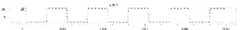
Translated fromKorean도 1 은 종래에 사용되던 쉬프트 레지스터의 회로도.1 is a circuit diagram of a shift register conventionally used.
도 2 는 액정표시장치의 패널상에 비정질실리콘 박막트랜지스터로 집적되어 형성된 본 발명의 제 1 실시예인 행구동회로에 사용되는 쉬프트 레지스터의 회로도.FIG. 2 is a circuit diagram of a shift register used in a row driving circuit according to the first embodiment of the present invention formed integrally with an amorphous silicon thin film transistor on a panel of a liquid crystal display.
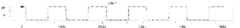
도 3a 내지 3e 는 도 2 에 도시된 제 1 실시예의 파형도.3A-3E are waveform diagrams of the first embodiment shown in FIG.
도 3f 는 도 3a 내지 도 3e 에서 발생할 수 있는 문제점을 설명하는 도면.FIG. 3F illustrates a problem that may occur in FIGS. 3A-3E.
도 3g 는 도 3f 는 도 3f 의 문제점을 해결할 수 있는 방안을 제시하는 도면.Figure 3g is a view showing a solution that can solve the problem of Figure 3f 3f.
도 4a 내지 4e 는 도 2 에 도시된 제 1 실시예의 다른 파형도.4A to 4E are other waveform diagrams of the first embodiment shown in FIG.
도 5와 6 은 본 발명의 제 2 실시예 및 제 3 실시예인 행구동회로에 사용되는 쉬프트 레지스터 회로도.5 and 6 are shift register circuit diagrams used in the row driving circuit which is the second and third embodiments of the present invention.
도 7a 내지 7f 은 TH=TL 인 경우에 있어서 도 6에 개시한 제 3 실시예의 동작을 설명하는 파형도.7A to 7F are waveform diagrams illustrating the operation of the third embodiment disclosed in FIG. 6 when TH = TL.
도 8a 내지 8e 는 TH〈 TL 인 경우에 있어서 도 6에 개시한 제 3 실시예의 동작을 설명하는 파형도.8A to 8E are waveform diagrams illustrating the operation of the third embodiment disclosed in FIG. 6 in the case of TH < TL.
도 9 내지 12 는 본 발명의 제 4 실시예 내지 7 실시예인 행구동회로에 사용되는 쉬프트 레지스터 회로도.9 to 12 are shift register circuit diagrams used for the row driving circuit which is the fourth to seventh embodiments of the present invention.
도 13 은 본 발명의 제 8 실시예인 행구동회로에 사용되는 쉬프트 레지스터 회로도.Fig. 13 is a shift register circuit diagram used in the row driving circuit as the eighth embodiment of the present invention.
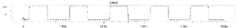
도 14a 내지 도 14f 는 도 13 에 도시된 회로의 파형도.14A-14F are waveform diagrams of the circuit shown in FIG.
도 15 및 도 16 은 도 13 의 회로에 있어서, 제 1 및 제 2 클락신호의 고전압 레벨 구간(TH)와 저전압 레벨 구간(TL)이 같은 경우 및 고전압 레벨 구간이 저전압 레벨 구간보다 작은 경우에 대한 각 단자(a, b) 전압의 HSPICE 시뮬레이션 파형도.15 and 16 illustrate a case in which the high voltage level section TH and the low voltage level section TL of the first and second clock signals are the same, and the high voltage level section is smaller than the low voltage level section in the circuit of FIG. 13. HSPICE simulation waveform diagram of voltage of each terminal (a, b).
도 17a 내지 도 17f 는 제 1 및 제 2 클락신호의 하이 레벨구간과 로우 레벨구간이 동일한 경우에 있어서 도 13 에 도시된 회로의 HSPICE 시뮬레이션 파형도.17A to 17F are HSPICE simulation waveform diagrams of the circuit shown in FIG. 13 when the high level section and the low level section of the first and second clock signals are the same.
도 18a 내지 도 18f 는 제 1 및 제 2 클락신호의 하이 레벨구간이 로우 레벨구간보다 작은 경우에 있어서 도 13 에 도시된 회로의 HSPICE 시뮬레이션 파형도.18A to 18F are HSPICE simulation waveform diagrams of the circuit shown in FIG. 13 when the high level section of the first and second clock signals is smaller than the low level section.
도 19은 본 발명의 제 9 실시예에 따른 쉬프트 레지스터의 회로도.19 is a circuit diagram of a shift register according to the ninth embodiment of the present invention.
도 20은 본 발명의 제 10 실시예에 따른 쉬프트 레지스터의 회로도.20 is a circuit diagram of a shift register according to a tenth embodiment of the present invention.
본 발명은 액정표시장치(LCD)의 행구동회로에 사용되는 쉬프트 레지스터에 관한 것으로, 특히 LCD 패널상에 비정질실리콘 박막트랜지스터로 집적되어 형성된 행구동회로에 사용되는 쉬프트 레지스터에 관한 것이다.BACKGROUND OF THE
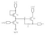
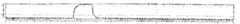
도 1 은 종래에 사용되던 쉬프트 레지스터의 회로도이다.1 is a circuit diagram of a shift register used in the related art.
도시된 바와같이, 종래의 쉬프트 레지스터는 제 1 트랜지스터(Tp)와 제 2 트랜지스터(Td), 제 3 트랜지스터(Tl)로 구성된다. 제 1 트랜지스터의 드레인과 게이트는 공통연결 단자이고, 제 1 트랜지스터의 소오스는 제 2 트랜지스터의 드레인 과 제 3 트랜지스터의 게이트에 공통 연결된다. 제 1 트랜지스터의 드레인은 (n-1)번째 게이트 라인 전압공급단자와 연결되며, 제 2 트랜지스터의 게이트는 (n+1)번째 게이트 라인 전압공급단자와 연결되며, 제 3 트랜지스터의 소오스 단자는 n 번째 게이트 라인으로 공급되는 전압을 출력하는 단자이다. 또한, 제 3 트랜지스터의 드레인에는 제 1 클락신호(clk1)가 인가되고, 제 3 트랜지스터의 게이트에는 제 2 클락신호(clk2)가 커패시터(C2)를 경유하여 인가된다. 제 3 트랜지스터의 게이트(노드 G)와 소오스간에는 커패시터(Cb)가 존재하며, 그 게이트(노드 G)와 드레인간에는 트랜지스터의 기생 커패시터(Cp)가 존재하며, 게이트(노드 G)의 소오스와 접지단자사이에는 부하 커패시터(C1)가 존재한다.As shown in the drawing, a conventional shift register includes a first transistor Tp, a second transistor Td, and a third transistor Tl. The drain and gate of the first transistor are common connection terminals, and the source of the first transistor is commonly connected to the drain of the second transistor and the gate of the third transistor. The drain of the first transistor is connected to the (n-1) th gate line voltage supply terminal, the gate of the second transistor is connected to the (n + 1) th gate line voltage supply terminal, and the source terminal of the third transistor is n The terminal outputs the voltage supplied to the first gate line. The first clock signal clk1 is applied to the drain of the third transistor, and the second clock signal clk2 is applied to the gate of the third transistor via the capacitor C2. The capacitor Cb exists between the gate (node G) and the source of the third transistor, and the parasitic capacitor Cp of the transistor exists between the gate (node G) and the drain, and the source and ground terminal of the gate (node G) There is a load capacitor C1 in between.
동작에 있어서, 신호(n-1)가 입력되면 제 1 트랜지스터(Tp)가 턴온되며, 따라서 신호(n-1)는 노드(G)로 전달되어 제 3 트랜지스터(Tl)를 충전시킨다. 다음, 신호(n-1)의 전위가 로우 전위(Voff)로 낮아지면 제 1 트랜지스터(Tp)는 턴오프되고 노드(G)는 충전 상태를 유지한다. 다음, 제 1 클락신호(clk1)가 고전압레벨이 되면서 커패시터(Cb)를 통해 부트스트랩 효과를 발생시켜 노드(G)의 전압을 더욱 상승시키게 된다. 따라서, 제 1 클락신호(clk1)의 고전압 레벨을 완전히 출력단(n)으로 출력시켜 패널 어레이의 n번째 행을 턴온시키게 된다. 마지막으로, 제 1 클락신호(clk1)가 저전압레벨이 되면서 제 3 트랜지스터(Tl)를 통해 패널 어레이의 n 번째 행을 방전시키게 되고, 신호(n+1)는 고전압 레벨이 되면서 제 2트랜지스터(Tl)를 통하여 노드(G)를 방전시켜 제 3 트랜지스터(Tl)를 오프시킨다.In operation, when the signal n-1 is input, the first transistor Tp is turned on, and thus the signal n-1 is transmitted to the node G to charge the third transistor Tl. Next, when the potential of the signal n-1 is lowered to the low potential Voff, the first transistor Tp is turned off and the node G maintains a charging state. Next, as the first clock signal clk1 becomes a high voltage level, a bootstrap effect is generated through the capacitor Cb to further increase the voltage of the node G. Therefore, the high voltage level of the first clock signal clk1 is completely output to the output terminal n to turn on the nth row of the panel array. Finally, as the first clock signal clk1 becomes the low voltage level, the n th row of the panel array is discharged through the third transistor Tl, and the signal n + 1 becomes the high voltage level and the second transistor Tl becomes the high voltage level. Node G is discharged to turn off third transistor Tl.
이러한 종래의 쉬프트 레지스터를 패널상에 집적하여 사용하는 경우, 회로 동작시, 클락신호(clk1)의 영향으로 제 3 트랜지스터(Tl)의 드레인과 게이트간의 기생 커패시터(Cp)를 통해 노드(G)가 부트스트랩 되는 것을 방지하기 위하여 노드(G)에 연결된 커패시터(C2)를 통해 위상이 정반대인 클락신호(clk2)를 입력하는 방식을 취하고 있다. 그러나, 이 효과는 n 번째 행을 선택해야 하는 경우, 부트스트랩 효과를 감소시키는 원인이 되고 있다. 이 때문에, 부트스트랩 효과를 극대화하기 위해서 커패시터(Cb)를 크게할 필요가 있었으며, 이는 커패시터 형성을 위해 더 큰 면적을 필요로 하게 되는 문제점을 초래하고 있다.In the case where the conventional shift register is integrated and used on the panel, the node G is connected through the parasitic capacitor Cp between the drain and the gate of the third transistor Tl under the influence of the clock signal clk1 during the circuit operation. In order to prevent the bootstrap, the clock signal clk2 having the opposite phase is input through the capacitor C2 connected to the node G. However, this effect causes the bootstrap effect to be reduced when the nth row is to be selected. For this reason, in order to maximize the bootstrap effect, it was necessary to increase the capacitor Cb, which causes a problem in that a larger area is required for capacitor formation.
본 발명은 전술한 문제점을 해결하기 위하여 제안된 것으로, n 번째 행을 선택하는 경우 부트스트랩 커패시터(Cb)가 부트스트랩 효과를 증가시키지만, 선택되지 않아야 하는 경우에는 부트스트랩 커패시터(Cb)가 출력단 트랜지스터의 드레인과 게이트간의 기생 커패시터로 인한 부트스트랩 효과를 감소시킬 수 있다는 점을 이용한 것으로, 일정한 커패시터 (Cb)를 사용함과 동시에 커패시터(C2)를 제거한 쉬프트 레지스터를 제공하고자 한다.The present invention has been proposed to solve the above-described problems. When the nth row is selected, the bootstrap capacitor Cb increases the bootstrap effect, but when it should not be selected, the bootstrap capacitor Cb is an output transistor. By taking advantage of the fact that the bootstrap effect due to the parasitic capacitor between the drain and the gate of the transistor can be reduced, the present invention provides a shift resistor using a constant capacitor (Cb) and removing the capacitor (C2).
또한, 본 발명에서는 커패시터(C2)의 제거로 인하여 출력단 트랜지스터의 게이트 전압이 불안정해질 수 있는 요인을 제거하기 위하여 방전 트랜지스터(Td)의 게이트에 클락신호(clk2)를 인가함으로써 주기적으로 출력단 트랜지스터의 게이트 전압을 오프 레벨로 떨어뜨릴 수 있는 쉬프트 레지스터를 제공하고자 한다.In addition, in the present invention, the clock signal of the output transistor is periodically applied by applying the clock signal clk2 to the gate of the discharge transistor Td in order to eliminate a factor in which the gate voltage of the output transistor may become unstable due to the removal of the capacitor C2. We want to provide a shift resistor that can drop the voltage to the off level.
또한, 본 발명에서는 커패시터(C2)의 제거로 인하여 출력단 트랜지스터가 매우 빠르게 방전되어 출력(n)이 완전히 방전되지 않는 것을 방지하기 위하여 방전 트랜지스터의 W/L 를 작게 설계한 쉬프트 레지스터를 제공하고자 한다.In addition, the present invention is to provide a shift resistor designed to reduce the W / L of the discharge transistor in order to prevent the output transistor is discharged very quickly due to the removal of the capacitor (C2) so that the output (n) is not completely discharged.
상기 목적을 이루기 위한 본 발명의 제 1 실시예인 액정구동장치의 행구동회로에 사용되는 쉬프트 레지스터는, 제 1 내지 3 트랜지스터를 포함하며,상기 제 1 트랜지스터의 드레인과 게이트는 연결되며,상기 제 1 트랜지스터의 소오스와 상기 제 2 트랜지스터의 드레인과 상기 제 3 트랜지스터의 게이트는 공통 연결되며,상기 제 2 트랜지스터의 소오스는 저전압인 오프전압에 연결되며,상기 제 3 트랜지스터의 게이트와 소오스간에는 커패시터가 연결되며,상기 제 1 트랜지스터의 드레인에는 n-1 번째 게이트 라인 전압공급단자와 연결되며,상기 제 3 트랜지스터의 드레인에는 제 1 클락신호가 인가되고, 상기 제 2 트랜지스터의 게이트에는 제 2 클락신호가 인가되며, 상기 제 3 트랜지스터의 소오스는 n 번째 게이트 라인 전압공급단자이며, 상기 제 1 및 제 2 클락신호의 위상은 상호 반전된 상태이며, 상기 제 1 및 제 2 클락신호의 하이 레벨 구간은 로우 레벨 구간보다 같거나 작은 것을 특징으로 한다.The shift register used in the row driving circuit of the liquid crystal driving apparatus according to the first embodiment of the present invention for achieving the above object comprises a first to third transistors, the drain and the gate of the first transistor is connected, the first transistor A source of the second transistor and a gate of the third transistor are commonly connected, a source of the second transistor is connected to an off voltage having a low voltage, and a capacitor is connected between the gate and the source of the third transistor, A drain of the first transistor is connected to an n−1 th gate line voltage supply terminal, a first clock signal is applied to a drain of the third transistor, a second clock signal is applied to a gate of the second transistor, The source of the third transistor is an n-th gate line voltage supply terminal, and the first and second The phase of the clock signal is inverted with each other, and the high level sections of the first and second clock signals are the same or smaller than the low level sections.
본 발명의 제 2 실시예는 제 1 실시예와 관련하여 상기 제 3 트랜지스터의 소오스와 상기 오프전압 사이에 연결된 제 4 트랜지스터를 더 구비하며, 상기 제 4 트랜지스터의 게이트에는 상기 제 2 클락신호가 인가되는 것을 특징으로 한다.The second embodiment of the present invention further comprises a fourth transistor connected between the source of the third transistor and the off voltage in relation to the first embodiment, wherein the second clock signal is applied to a gate of the fourth transistor. It is characterized by.
본 발명의 제 3 실시예는 제 1 실시예와 관련하여, 상기 제 2 트랜지스터와 병렬로 연결된 제 4 트랜지스터를 더 포함하며, 상기 제 4 트랜지스터의 게이트는 n+1 번째 게이트 라인 전압공급단자와 연결되는 것을 특징으로 한다.The third embodiment of the present invention further includes a fourth transistor connected in parallel with the second transistor in relation to the first embodiment, wherein a gate of the fourth transistor is connected to an n + 1 th gate line voltage supply terminal. It is characterized by.
본 발명의 제 4 실시예는 제 1 실시예와 관련하여, 상기 제 3 트랜지스터의 소오스와 상기 오프전압 사이에 연결된 제 4 트랜지스터를 더 구비하며, 상기 제 4 트랜지스터의 게이트는 n+1 번째 게이트 라인 전압공급단자와 연결되는 것을 특징으로 한다.A fourth embodiment of the present invention further comprises a fourth transistor connected between the source of the third transistor and the off voltage, in relation to the first embodiment, wherein the gate of the fourth transistor is an n + 1 th gate line. It is characterized in that connected to the voltage supply terminal.
본 발명의 제 5 실시예는 제 4 실시예와 관련하여, 상기 제 2 트랜지스터와 병렬로 연결된 제 5 트랜지스터를 더 포함하며, 상기 제 5 트랜지스터의 게이트는 n+1 번째 게이트 라인 전압공급단자와 연결되는 것을 특징으로 한다.In accordance with a fourth embodiment, the fifth embodiment of the present invention further includes a fifth transistor connected in parallel with the second transistor, wherein a gate of the fifth transistor is connected to an n + 1 th gate line voltage supply terminal. It is characterized by.
본 발명의 제 6 실시예는 제 1 실시예와 관련하여, 상기 제 3 트랜지스터의 소오스와 상기 오프전압 사이에 연결된 제 4 트랜지스터와, 상기 제 2 트랜지스터와 병렬로 연결된 제 5 트랜지스터를 더 포함하며, 제 4 트랜지스터의 게이트에는 제 2 클락이 인가되고 제 5 트랜지스터의 게이트에는 n+1 번째 게이트 라인 전압이 인가된다.A sixth embodiment of the present invention further includes a fourth transistor connected between a source of the third transistor and the off voltage, and a fifth transistor connected in parallel with the second transistor in relation to the first embodiment. The second clock is applied to the gate of the fourth transistor and the n + 1 th gate line voltage is applied to the gate of the fifth transistor.
본 발명의 제 7 실시예는 제 1 실시예와 관련하여, 상기 제 3 트랜지스터의 소오스와 상기 오프전압 사이에 연결된 제 4 트랜지스터와, 상기 제 2 트랜지스터와 병렬로 연결된 제 5 트랜지스터와, 상기 제 4 트랜지스터와 병렬로 연결된 제 6 트랜지스터를 더 포함하며, 상기 제 4 트랜지스터의 게이트와 상기 제 5 트랜지스터의 게이트는 n+1 번째 게이트 라인 전압공급단자와 연결되며, 상기 제 6 트랜지스터의 게이트에는 상기 제 2 클락이 인가되는 것을 특징으로 한다.
본 발명의 제 8 실시예인 액정표시장치의 행구동회로에 사용되는 쉬프트 레지스터는, 제 1 내지 6 트랜지스터를 포함하며, 상기 제 1 트랜지스터의 드레인과 게이트는 연결되며, 제 1 트랜지스터의 소오스와 상기 제 2 트랜지스터의 드레인과 상기 제 6 트랜지스터의 게이트는 공통 연결되며, 상기 제 2 트랜지스터의 소오스는 저전압인 오프전압에 연결되며, 상기 제 4 트랜지스터의 드레인은 단자에 연결되며, 소오스는 저전압인 오프전압에 연결되며, 상기 제 3 트랜지스터의 드레인과 게이트는 연결되며, 상기 제 3 트랜지스터의 소오스와 상기 제 4 트랜지스터의 게이트와 상기 제 5 트랜지스터의 드레인은 공통 연결되며, 상기 제 5 트랜지스터의 게이트는 단자에 연결되며, 소오스는 저전압인 오프전압에 연결되며, 상기 제 1 트랜지스터의 드레인은 n-1 번째 게이트 라인 전압 단자와 연결되며,상기 제 2 트랜지스터의 게이트는 n+1 번째 게이트 라인 전압 단자와 연결되며, 제 6 트랜지스터의 소오스는 n 번째 게이트 라인 전압 단자이며, 상기 제 3 트랜지스터의 드레인에는 제 2 클락신호가 인가되고, 상기 제 6 트랜지스터의 드레인에는 제 1 클락신호가 인가되며, 상기 제 1 및 제 2 클락신호의 위상은 상호 반전된 상태이며,상기 제 1 및 제 2 클락신호의 하이 레벨구간은 로우 레벨 구간보다 작거나 같은 것을 특징으로 한다.
본 발명의 제 9 실시예는 제 8 실시예와 관련하여, 상기 제 6 트랜지스터의 소오스와 상기 오프전압사이에 연결된 제 7 트랜지스터를 더 포함하며, 상기 제 7 트랜지스터의 게이트에는 상기 제 2 클락신호 또는 상기 n+1 번째 게이트 라인 전압공급단자와 연결되어 있는 것을 특징으로 한다.
본 발명의 제 9 실시예는 제 8 실시예와 관련하여, 상기 제 6 트랜지스터의 소오스와 상기 오프전압사이에 연결된 제 7 트랜지스터를 더 구비하며, 상기 제 7 트랜지스터의 게이트는 상기 제 5 트랜지스터의 드레인과 연결되어 있는 것을 특징으로 한다.A seventh embodiment of the present invention relates to a fourth transistor connected between a source of the third transistor and the off voltage, a fifth transistor connected in parallel with the second transistor, and the fourth embodiment in relation to the first embodiment. And a sixth transistor connected in parallel with the transistor, wherein a gate of the fourth transistor and a gate of the fifth transistor are connected to an n + 1 th gate line voltage supply terminal, and a gate of the sixth transistor is connected to the second transistor. It is characterized in that the clock is applied.
The shift register used in the row driving circuit of the liquid crystal display according to the eighth embodiment of the present invention includes first to sixth transistors, the drain and the gate of the first transistor are connected, and the source and the second of the first transistor are connected. A drain of the transistor and a gate of the sixth transistor are commonly connected, a source of the second transistor is connected to an off voltage of a low voltage, a drain of the fourth transistor is connected to a terminal, and a source is connected to an off voltage of a low voltage. A drain and a gate of the third transistor are connected, a source of the third transistor, a gate of the fourth transistor and a drain of the fifth transistor are commonly connected, and a gate of the fifth transistor is connected to a terminal. The source is connected to an off voltage which is a low voltage, and the drain of the first transistor is n-1. A gate of the second transistor is connected to an n + 1th gate line voltage terminal, a source of the sixth transistor is an nth gate line voltage terminal, and a drain of the third transistor A second clock signal is applied, a first clock signal is applied to the drain of the sixth transistor, and phases of the first and second clock signals are inverted with each other, and a high level of the first and second clock signals is applied. The interval may be smaller than or equal to the low level interval.
A ninth embodiment of the present invention further includes a seventh transistor connected between the source of the sixth transistor and the off voltage in relation to the eighth embodiment, wherein the gate of the seventh transistor includes the second clock signal or And the n + 1 th gate line voltage supply terminal.
A ninth embodiment of the present invention further includes a seventh transistor connected between the source of the sixth transistor and the off voltage in relation to the eighth embodiment, wherein the gate of the seventh transistor is a drain of the fifth transistor. It is characterized in that connected with.
(실시예)(Example)
이하, 도면을 참조하여 본 발명의 실시예에 대하여 보다 구체적으로 설명하기로 한다.Hereinafter, exemplary embodiments of the present invention will be described in detail with reference to the accompanying drawings.
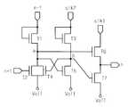
도 2 는 액정표시장치의 패널상에 비정질실리콘 박막트랜지스터로 집적되어 형성된 본 발명의 제 1 실시예인 행구동회로에 사용되는 쉬프트 레지스터에 관한 것이다.2 is related to a shift register used in a row driving circuit according to a first embodiment of the present invention formed by integrating an amorphous silicon thin film transistor on a panel of a liquid crystal display.
도시된 바와같이, 본 발명에 따른 제 1 실시예인 액정구동장치의 행구동회로에 사용되는 쉬프트 레지스터는, 제 1 내지 3 트랜지스터(Tc, Td, Tf)를 포함하며,상기 제 1 트랜지스터(Tc)의 드레인과 게이트는 연결되며,상기 제 1 트랜지스터의 소오스와 상기 제 2 트랜지스터(Td)의 드레인과 상기 제 3 트랜지스터(Tf)의 게이트는 공통 연결되며,상기 제 2 트랜지스터의 소오스는 저전압인 오프전압(Voff)에 연결되며,상기 제 3 트랜지스터(Tf)의 게이트와 소오스간에는 커패시터(C)가 연결되며,상기 제 1 트랜지스터의 드레인은 n-1 번째 게이트 라인 전압공급단자와 연결되며,상기 제 3 트랜지스터의 드레인에는 제 1 클락신호(clk1)가 인가되고, 상기 제 2 트랜지스터의 게이트에는 제 2 클락신호(clk2)가 인가되며, 상기 제 3 트랜지스터의 소오스는 n 번째 게이트 라인 전압공급단자이며, 상기 제 1 및 제 2 클락신호의 위상은 상호 반전된 상태이다.As shown, the shift register used in the row driving circuit of the liquid crystal drive device according to the first embodiment of the present invention includes first to third transistors Tc, Td, and Tf, and the first transistor Tc of the first transistor Tc. A drain and a gate are connected to each other, a source of the first transistor, a drain of the second transistor Td, and a gate of the third transistor Tf are connected in common, and a source of the second transistor is an off voltage having a low voltage. Voff), a capacitor (C) is connected between the gate and the source of the third transistor (Tf), the drain of the first transistor is connected to the n-1 th gate line voltage supply terminal, the third transistor A first clock signal clk1 is applied to a drain of the second transistor, a second clock signal clk2 is applied to a gate of the second transistor, and the source of the third transistor is an n-th gate line voltage. It is a supply terminal, and the phases of the first and second clock signals are inverted with each other.
도 2 에 개시된 쉬프트 레지스터의 동작은 도 3a 내지 3e, 도 4a 내지 4e 를 참조하여 설명하기로 한다.The operation of the shift register disclosed in FIG. 2 will be described with reference to FIGS. 3A to 3E and 4A to 4E.
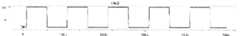
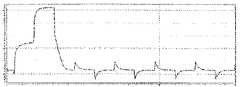
도 3a 내지 3e 는 TH=TL 인 경우에 있어서 도 2 에 개시된 쉬프트 레지스터의 제 1 및 제 2 클락신호(clk1, clk2), n-1 번째 게이트 라인 전압, 제 3 트랜지스터(Tf)의 게이트 단자(a)의 전압, 및 n 번째 게이트 라인 전압의 파형도를 도시하며, 도 4a 내지 4e 는 TH〈 TL 인 경우에 있어서 도 2 에 개시된 쉬프트 레지스터의 제 1 및 제 2 클락신호(clk1, clk2), n-1 번째 게이트 라인 전압, 제 3 트랜지스터(Tf)의 게이트 단자(a)의 전압, 및 n 번째 게이트 라인 전압의 파형도를 도시한다.3A to 3E illustrate the first and second clock signals clk1 and clk2 of the shift register disclosed in FIG. 2, the n−1 th gate line voltage, and the gate terminal of the third transistor Tf when TH = TL. The waveform of a) and the n-th gate line voltage are shown, and FIGS. 4A to 4E show the first and second clock signals clk1 and clk2 of the shift register disclosed in FIG. 2 when TH <TL; The waveform diagram of the n-th gate line voltage, the voltage of the gate terminal a of the third transistor Tf, and the n-th gate line voltage is shown.
참고로, 제 1 클락신호(clk1)의 파형도에서, TH 는 고전압레벨 구간을, TL 은 저전압레벨 구간을 나타낸다. 마찬가지로, 제 2 클락신호(clk2)의 파형도에서, TH 는 고전압레벨 구간을, TL 은 저전압레벨 구간을 나타낸다. 이때, 도 2 의 회로는 TH ≤TL 이고, 제 1 및 제 2 클락신호가 상호 반전된 위상을 가지며, 동시에 고전압 레벨을 갖지 않는 경우에만 정상 동작을 한다.For reference, in the waveform diagram of the first clock signal clk1, TH represents a high voltage level section and TL represents a low voltage level section. Similarly, in the waveform diagram of the second clock signal clk2, TH represents a high voltage level section and TL represents a low voltage level section. At this time, the circuit of FIG. 2 is TH ≤ TL, and the normal operation is performed only when the first and second clock signals have inverted phases and do not have a high voltage level.
도 3a 내지 3e 에 도시된 바와같이, n-1 번째 게이트 라인 전압은 제 2 클락신호가 TH 구간일때 고전압 레벨 구간을 갖는다. n-1 번째 게이트 라인 전압이 인가되면, 제 1 트랜지스터(Tc)가 턴온되고 따라서 제 3 트랜지스터의 게이트 단자(a)는 도면과 같이 충전된다. 이때, 제2 클락신호(clk2)에 의하여 제 2 트랜지스터(Td)도 턴온되어 있으므로 단자(a)의 전압이 Voff 레벨로 하강할 우려가 있다. 이 경우, 본 발명의 목적을 달성하기 위하여, 단자(a)의 전위를 n-1 번째 게이트 라인 전압에 근접시킬 필요가 있으므로, 제 1 트랜지스터(Tc)의 W/L 를 제 2 트랜지스터(Td)의 W/L 보다 크게 하는 것이 바람직하다.As shown in FIGS. 3A to 3E, the n−1 th gate line voltage has a high voltage level section when the second clock signal is a TH section. When the n−1 th gate line voltage is applied, the first transistor Tc is turned on and thus the gate terminal a of the third transistor is charged as shown in the drawing. At this time, since the second transistor Td is also turned on by the second clock signal clk2, the voltage of the terminal a may drop to the Voff level. In this case, in order to achieve the object of the present invention, it is necessary to bring the potential of the terminal a close to the n−1 th gate line voltage, so that W / L of the first transistor Tc is set to the second transistor Td. It is preferable to make it larger than W / L.
다음, 단자(a)가 충전되면 제 3 트랜지스터(Tf)가 턴온되어 제 3 트랜지스터(Tf)의 소오스는 제 1 클락신호(clk1)의 전압레벨을 따라간다. 제 2 클락신호(clk2)가 고전압 레벨인 경우, 제 1 클락신호(clk1)는 저전압 레벨이므로, 제 3 트랜지스터(Tf)의 소오스 전위인 n 번째 게이트 라인 전압은 도 3 에 도시된 바와같이 Voff 가 되며 따라서 패널 어레이의 n 번째 게이트는 오프상태를 유지한다.Next, when the terminal a is charged, the third transistor Tf is turned on so that the source of the third transistor Tf follows the voltage level of the first clock signal clk1. When the second clock signal clk2 is at the high voltage level, since the first clock signal clk1 is at the low voltage level, the n-th gate line voltage, which is the source potential of the third transistor Tf, is Voff as shown in FIG. Thus, the nth gate of the panel array remains off.
다음, 제 2 클락신호(clk2)가 저전압 레벨로 되면 제 2 트랜지스터(Td)는 턴오프되고, n-1 번째 게이트 라인 전압은 Voff 의 저전압 레벨이 되면서 제 1 트랜지스터(Tc)도 오프되어 단자(a)는 충전상태를 유지한다.Next, when the second clock signal clk2 reaches the low voltage level, the second transistor Td is turned off, the n−1 th gate line voltage becomes the low voltage level of Voff, and the first transistor Tc is also turned off. a) maintains the state of charge.
다음, 제 1 클락신호(clk1)가 고전압 레벨이 되면서 커패시터(C)를 통하여 부트스트랩 효과를 일으켜 단자(a)의 전압을 더욱 상승시키게 된다. 따라서, 제 1 클락신호(clk1)가 고전압 레벨을 완전히 n 번째 게이트 라인 전압으로 내보내어 패널 어레이의 n번째 게이트 라인을 턴온시킨다.Next, as the first clock signal clk1 becomes a high voltage level, a bootstrap effect is caused through the capacitor C to further increase the voltage of the terminal a. Accordingly, the first clock signal clk1 turns on the n-th gate line of the panel array by completely outputting the high voltage level to the n-th gate line voltage.
마지막으로, 제 1 클락신호(clk1)가 저전압 레벨이 되면서 제 3 트랜지스터 (Tf)를 통해 패널 어레이의 n번째 게이트 라인을 방전시켜 저전압 레벨인 Voff 로 떨어뜨리고, 제 2 클락신호(clk2)는 고전압 레벨이 되면서 제 2 트랜지스터(Td)를 통하여 단자(a)의 전압을 Voff 로 떨어뜨려 제 3 트랜지스터 (Tf)를 턴오프시킨다. 이렇게 하여, 쉬프트 레지스터의 한 단계 동작이 완료된다.Finally, as the first clock signal clk1 becomes the low voltage level, the n-th gate line of the panel array is discharged to the low voltage level Voff through the third transistor Tf, and the second clock signal clk2 becomes the high voltage. At the level, the voltage of the terminal a is dropped to Voff through the second transistor Td to turn off the third transistor Tf. In this way, one step operation of the shift register is completed.
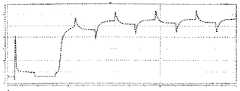
다음 도 4a 내지 4e 에 대하여 설명한다. 전술한 바와같이, 도 4a 내지 4e 는 TH〈 TL 인 경우에 있어서 도 2 에 개시된 쉬프트 레지스터의 제 1 및 제 2 클락신호(clk1, clk2), n-1 번째 게이트 라인 전압, 제 3 트랜지스터(Tf)의 게이트 단자(a)의 전압, 및 n 번째 게이트 라인 전압의 파형도를 도시한다.Next, FIGS. 4A to 4E will be described. As described above, FIGS. 4A to 4E show the first and second clock signals clk1 and clk2 of the shift register disclosed in FIG. 2, the n−1 th gate line voltage, and the third transistor Tf when TH <TL. Shows a waveform diagram of the voltage at the gate terminal a and the n-th gate line voltage.
일반적으로, 도 3a 내지 3e 에서와같이, TH=TL 조건하에서 쉬프트 레지스터를 동작시키는 경우, n-1 번째 게이트 라인 전압과 n 번째 게이트 라인 전압이 동시에 턴온되는 구간이 존재하며, 이 때문에 액정표시장치의 화면상에 원하지 않는 결과가 초래되어 신뢰성이 떨어지는 문제점이 있다. 이에 대하여는 도 3f 을 참조하여 설명한다.In general, when the shift register is operated under the condition TH = TL as shown in FIGS. 3A to 3E, there is a section in which the n−1 th gate line voltage and the n th gate line voltage are turned on at the same time. There is a problem that the undesired result is caused on the screen of the reliability is low. This will be described with reference to FIG. 3F.
도 3f 에 도시된 바와같이, 제 1 및 제 2 클락신호의 위상이 상호 반전된 상태이고, TH=TL 인 경우, n-1 번째 게이트 라인 전압의 출력 지연(일반적으로 RC 지연)으로 인하여 n-1 번째 게이트 라인 전압과 n 번째 게이트 라인 전압이 동시에 턴온되어 있는 구간이 존재할 수 있으며, 이 경우 액정표시장치의 화면상에는 원하지 않는 결과가 나타나 신뢰성이 떨어질 수 있다. 이러한 문제점을 해결할 수 있는 방법으로는 도 3g 에서와같이 TH 구간은 TL 구간보다 협소하게 하여 해결할 수 있다.As shown in FIG. 3F, when the phases of the first and second clock signals are inverted with each other, and TH = TL, n − due to an output delay (generally RC delay) of the n−1 th gate line voltage. There may exist a section in which the first gate line voltage and the nth gate line voltage are turned on at the same time. In this case, undesired results may appear on the screen of the liquid crystal display, thereby lowering reliability. As a method for solving this problem, as shown in FIG. 3g, the TH section can be solved by making it narrower than the TL section.
도 3g 에 도시된 바와같이, 제 1 및 제 2 클락신호가 동시에 하이 레벨 구간을 갖지 않도록 일정 여유를 제공하여(즉, TH〈 TL 조건을 만족시킴으로써), n-1 번째 게이트 라인 전압과 n 번째 게이트 라인 전압이 동시에 턴온되어 있는 구간이 존재하지 않도록 할 수 있다.As shown in Fig. 3G, by providing a certain margin so that the first and second clock signals do not have a high level section at the same time (i.e., satisfying the condition of TH < TL), the n-1 th gate line voltage and the n th It is possible to prevent the section in which the gate line voltages are turned on at the same time.
도 4a 내지 4e 는 도 3a 내지 3e 에 나타날 수 있는 문제점을 해결하기 위하여, 제 1 클락신호(clk1)와 제 2 클락신호(clk2)가 TH〈 TL 의 조건을 만족하도록 함으로써 n-1 번째 게이트 라인 전압과 n 번째 게이트 라인 전압이 동시에 턴온되는 구간이 생기지 아니하도록 하였으며, 이는 도 4a 내지 4e 의 파형도로부터 알 수 있다.4A to 4E illustrate an n-1 th gate line by satisfying a condition of TH <TL with the first clock signal clk1 and the second clock signal clk2 to solve the problems that may appear in FIGS. 3A through 3E. The section in which the voltage and the n-th gate line voltage are simultaneously turned on does not occur, which can be seen from the waveform diagrams of FIGS. 4A to 4E.
도 5는 액정표시장치의 패널상에 비정질실리콘 박막트랜지스터로 집적되어 형성된 본 발명의 제 2 실시예인 행구동회로에 사용되는 쉬프트 레지스터에 관한 것이다.FIG. 5 relates to a shift register used in a row driving circuit according to a second embodiment of the present invention formed by integrating an amorphous silicon thin film transistor on a panel of a liquid crystal display.
도시된 바와같이, 본 발명의 제 2 실시예는 제 1 실시예와 관련하여 제 1 실시예의 제 3 트랜지스터(Tf)의 소오스와 오프전압(Voff) 사이에 연결되는 제 4 트랜지스터(To)를 더 구비하며, 제 4 트랜지스터의 게이트에는 제 2 클락신호(clk2)가 인가된다. 제 1 실시예의 경우, 제 3 트랜지스터(Tf)의 게이트 전압의 방전은 n 번째 게이트 라인의 오프상태가 안정화될 정도로 빠르면서도 n 번째 게이트 라인 전압이 완전히 방전되어 오프상태가 될 수가 있을 정도로 느려야 한다. 따라서, 제 2 트랜지스터(Td)의 W/L 만으로 이를 조절하는 것은 쉽지 않다.As shown, the second embodiment of the present invention further comprises a fourth transistor To connected between the source of the third transistor Tf of the first embodiment and the off voltage Voff in relation to the first embodiment. The second clock signal clk2 is applied to the gate of the fourth transistor. In the case of the first embodiment, the discharge of the gate voltage of the third transistor Tf should be fast enough to stabilize the off state of the n-th gate line and slow enough to allow the n-th gate line voltage to be completely discharged. . Therefore, it is not easy to control this by only the W / L of the second transistor Td.
제 2 실시예는 제 1 실시예의 이러한 문제점을 보완한 것으로, 제 2 클락신호(clk2)에 의하여 제 4 트랜지스터(To)를 턴온시켜 n 번째 게이트 라인의 방전을 도움으로써 n 번째 게이트 라인의 전압이 제 2 트랜지스터(Td)의 W/L 에 영향을 덜 받으면서 완전히 방전되도록 한다.The second embodiment compensates for this problem of the first embodiment. The fourth transistor To is turned on by the second clock signal clk2 to assist the discharge of the n-th gate line, thereby reducing the voltage of the n-th gate line. The battery is completely discharged while being less affected by W / L of the second transistor Td.
또한, 제 1 실시예의 경우, 제 3 트랜지스터(Tf)가 오프된 상태라도 제 3 트랜지스터(Tf)의 게이트와 드레인 사이의 기생커패시터에 의해 제 1 클락신호(clk1)의 변화에 따라 부트스트랩이 발생하면, 제 3 트랜지스터(Tf)의 누설전류에 의해 n 번째 게이트 라인 전압이 조금씩 증가하는 문제점이 있었다. 그라나, 제 2 실시예에서는 제 4 트랜지스터(To)를 통해 주기적으로 n 번째 게이트 라인 전압을 방전시켜 줌으로써 n 번째 게이트 라인 전압이 지속적으로 오프레벨을 유지할 수 있도록 할 수 있다.In addition, in the case of the first embodiment, even when the third transistor Tf is turned off, a bootstrap occurs due to the change of the first clock signal clk1 by the parasitic capacitor between the gate and the drain of the third transistor Tf. In other words, the n-th gate line voltage increases little by little due to the leakage current of the third transistor Tf. However, in the second embodiment, the n-th gate line voltage may be continuously maintained at the off level by periodically discharging the n-th gate line voltage through the fourth transistor To.
도 6은 액정표시장치의 패널상에 비정질실리콘 박막트랜지스터로 집적되어 형성된 본 발명의 제 3 실시예인 행구동회로에 사용되는 쉬프트 레지스터에 관한 것이다.FIG. 6 relates to a shift register used in a row driving circuit according to a third embodiment of the present invention formed by integrating an amorphous silicon thin film transistor on a panel of a liquid crystal display.
도시된 바와같이, 본 발명의 제 3 실시예는 제 1 실시예와 관련하여, 제 1 실시예의 제 2 트랜지스터(Td)와 병렬로 연결된 제 4 트랜지스터(Td1)를 더 포함하며, 상기 제 4 트랜지스터(Td1)의 게이트는 n+1 번째 게이트 라인 전압공급단자와 연결된다.As shown, the third embodiment of the present invention further comprises a fourth transistor Td1 connected in parallel with the second transistor Td of the first embodiment, in relation to the first embodiment, wherein the fourth transistor The gate of Td1 is connected to the n + 1 th gate line voltage supply terminal.
제 1 실시예의 경우, 제 2 트랜지스터(Td)의 W/L 은 제 1 트랜지스터(Tc)의 W/L 보다 작아야 한다. 그러나, 제 2 트랜지스터(Td)의 W/L 이 너무 작으면 제 3 트랜지스터(Tf)의 게이트 단자(a) 전압의 방전이 n 번째 게이트 라인의 오프상태가 안정화될 정도로 빠르지 못하며, 반대로 제 2 트랜지스터(Td)의 W/L 이 너무 크면 제 1 트랜지스터(Tc)의 W/L 도 상대적으로 훨씬 커져 면적을 많이 차지하게 되는 문제점이 있다.In the case of the first embodiment, the W / L of the second transistor Td should be smaller than the W / L of the first transistor Tc. However, if the W / L of the second transistor Td is too small, the discharge of the voltage of the gate terminal a of the third transistor Tf is not so fast that the off state of the n-th gate line is stabilized. If the W / L of the Td is too large, the W / L of the first transistor Tc is relatively much larger, thus taking up a large area.
제 3 실시예는 제 1 실시예의 이러한 문제점을 보완한 것으로, 제 1 트랜지스터(Tc)의 W/L 가 커지지 않도록 제 2 트랜지스터(Td)의 W/L 를 작게 유지하면서도 제 3 트랜지스터(Tf)의 게이트 전압의 방전이 n 번째 게이트 라인의 오프상태가 안정화될 정도로 빠르도록 하기 위하여, n+1 번째 게이트 라인 전압을 피드백받아 제 4 트랜지스터(Td1)를 제어함으로써 제 3 트랜지스터(Tf)의 게이트 방전을 도와준다.The third embodiment compensates for this problem of the first embodiment, and keeps the W / L of the second transistor Td small so that the W / L of the first transistor Tc does not increase. In order for the discharge of the gate voltage to be fast enough that the off state of the n-th gate line is stabilized, the gate discharge of the third transistor Tf is controlled by feeding back the n + 1-th gate line voltage and controlling the fourth transistor Td1. help.
도 7a 내지 7f 은 TH=TL 인 경우에 있어서 도 6에 개시한 제 3 실시예의 동작을 설명하는 파형도이고, 도 8a 내지 8e 는 TH〈 TL 인 경우에 있어서 도 6에 개시한 제 3 실시예의 동작을 설명하는 파형도로서, 위에서 상술한 n+1 번째 게이트 라인 전압 파형도를 추가로 도시하고 있다는 점을 제외하고는 도 3a 내지 3e, 4a 내지 4e 에서 설명한 내용과 중첩되므로 반복적인 설명은 생략한다. 참고로, 도 4a 내지 4e 에서와 마찬가지로, 제 1 클락신호(clk1)와 제 1 클락신호(clk1)가 TH〈 TL 인 조건을 만족하는 경우, n-1 번째 게이트 라인 전압과 n 번째 게이트 라인 전압이 동시에 턴온되는 것을 방지하여 보다 신뢰성있는 동작이 가능함을 당업자는 알 수 있을 것이다.7A to 7F are waveform diagrams illustrating the operation of the third embodiment disclosed in FIG. 6 in the case of TH = TL, and FIGS. 8A to 8E illustrate the third embodiment disclosed in FIG. 6 in the case of TH <TL. As a waveform diagram illustrating the operation, the description is overlapped with those described in FIGS. 3A to 3E and 4A to 4E except that the n + 1 th gate line voltage waveform diagram described above is further illustrated. do. For reference, as in FIGS. 4A to 4E, when the first clock signal clk1 and the first clock signal clk1 satisfy a condition of TH <TL, the n−1 th gate line voltage and the n th gate line voltage It will be appreciated by those skilled in the art that more reliable operation is possible by preventing the turn on at the same time.
도 9는 액정표시장치의 패널상에 비정질실리콘 박막트랜지스터로 집적되어 형성된 본 발명의 제 4 실시예인 행구동회로에 사용되는 쉬프트 레지스터에 관한 것이다.FIG. 9 relates to a shift register used in a row driving circuit according to a fourth embodiment of the present invention formed by integrating an amorphous silicon thin film transistor on a panel of a liquid crystal display.
도시된 바와같이, 본 발명의 제 4 실시예는 제 1 실시예와 관련하여, 제 1 실시예의 제 3 트랜지스터(Tf)의 소오스와 오프전압(Voff) 사이에 연결된 제 4 트랜지스터(To1)를 더 구비하며, 상기 제 4 트랜지스터(To1)의 게이트는 n+1 번째 게이트 라인 전압공급단자와 연결된다.As shown, the fourth embodiment of the present invention further relates to the first embodiment further comprising a fourth transistor To1 connected between the source of the third transistor Tf of the first embodiment and the off voltage Voff. The gate of the fourth transistor To1 is connected to the n + 1 th gate line voltage supply terminal.
제 4 실시예의 경우, 도 5 에 도시된 제 2 실시예의 경우와 유사하게, n 번째 게이트 라인 전압이 제 2 트랜지스터(Td)의 W/L 에 영향을 덜 받으면서 완전하게 방전되도록 하기 위해 n+1 번째 게이트 라인 전압을 이용하여 제 4 트랜지스터(To1)를 턴온시켜 n 번째 게이트 라인 전압의 방전을 돕는다.In the case of the fourth embodiment, similar to the case of the second embodiment shown in FIG. 5, n + 1 so that the n-th gate line voltage is completely discharged while being less affected by the W / L of the second transistor Td. The fourth transistor To1 is turned on using the fourth gate line voltage to help discharge the nth gate line voltage.
도 10은 액정표시장치의 패널상에 비정질실리콘 박막트랜지스터로 집적되어 형성된 본 발명의 제 5 실시예인 행구동회로에 사용되는 쉬프트 레지스터에 관한 것이다.FIG. 10 relates to a shift register used in a row driving circuit according to a fifth embodiment of the present invention formed by integrating an amorphous silicon thin film transistor on a panel of a liquid crystal display.
도시된 바와같이, 본 발명의 제 5 실시예는 도 9 에 개시한 제 4 실시예와 관련하여, 제 4 실시예의 제 2 트랜지스터(Td)와 병렬로 연결된 제 5 트랜지스터(Td1)를 더 포함하며, 제 5 트랜지스터(Td1)의 게이트는 n+1 번째 게이트 라인 전압공급단자와 연결된다.As shown, the fifth embodiment of the present invention further includes a fifth transistor Td1 connected in parallel with the second transistor Td of the fourth embodiment with respect to the fourth embodiment disclosed in FIG. The gate of the fifth transistor Td1 is connected to the n + 1 th gate line voltage supply terminal.
추가된 제 5 트랜지스터(Td1)의 역할은 도 6에 개시된 제 3 실시예의 경우와 동일하므로 반복적인 설명은 생략하기로 한다.Since the role of the added fifth transistor Td1 is the same as that of the third embodiment disclosed in FIG. 6, repeated description thereof will be omitted.
도 11 과 12 는 액정표시장치의 패널상에 비정질실리콘 박막트랜지스터로 집적되어 형성된 본 발명의 제 6 실시예 및 제 7 실시예인 행구동회로에 사용되는 쉬프트 레지스터에 관한 것이다.11 and 12 relate to shift registers used in the row driving circuits of the sixth and seventh embodiments of the present invention, which are formed by integrating an amorphous silicon thin film transistor on a panel of a liquid crystal display.
도시된 바와같이, 본 발명의 제 6 실시예는 제 1 실시예의 제 3 트랜지스터(Tf)의 소오스와 오프전압(Voff) 사이에 연결된 제 4 트랜지스터(To)와, 제 2 트랜지스터(Td)와 병렬로 연결된 제 5 트랜지스터(Td1)를 더 포함하며, 제 4 트랜지스터의 게이트에는 제 2 클락이 인가되고 제 5 트랜지스터의 게이트에는 n+1 번째 게이트 라인 전압이 인가된다. 제 4 및 제 5 트랜지스터의 기능은 지금까지 설명한 실시예의 경우와 동일하므로 더 이상의 기능에 대한 설명은 생략한다.As shown, the sixth embodiment of the present invention is in parallel with the fourth transistor To and the second transistor Td connected between the source and the off voltage Voff of the third transistor Tf of the first embodiment. A fifth transistor Td1 is further connected to the gate of the fourth transistor, and a second clock is applied to the gate of the fourth transistor, and an n + 1 th gate line voltage is applied to the gate of the fifth transistor. Since the functions of the fourth and fifth transistors are the same as those of the embodiment described so far, descriptions of further functions will be omitted.
도시된 바와같이, 본 발명의 제 7 실시예는 제 1 실시예의 제 3 트랜지스터(Tf)의 소오스와 오프전압(Voff) 사이에 연결된 제 4 트랜지스터(To1)와, 상기 제 2 트랜지스터(Td)와 병렬로 연결된 제 5 트랜지스터(Td1)와, 상기 제 4 트랜지스터(To1)와 병렬로 연결된 제 6 트랜지스터(To)를 더 포함하며, 제 4 트랜지스터의 게이트와 제 5 트랜지스터(Td1)의 게이트는 n+1 번째 게이트 라인 전압공급단자와 연결되며, 제 6 트랜지스터(To)의 게이트에는 제 2 클락이 인가된다. 제 7 실시예의 제 4 내지 6 트랜지스터의 기능은 지금까지 설명한 실시예의 경우와 동일하므로 더 이상의 기능에 대한 설명은 생략하기로 한다.As shown, the seventh embodiment of the present invention is the fourth transistor To1 connected between the source and the off voltage Voff of the third transistor Tf of the first embodiment, and the second transistor Td and the second transistor Td. And a fifth transistor Td1 connected in parallel and a sixth transistor To connected in parallel with the fourth transistor To1, wherein the gate of the fourth transistor and the gate of the fifth transistor Td1 are n +. The second clock is connected to the first gate line voltage supply terminal, and a second clock is applied to the gate of the sixth transistor To. Since the functions of the fourth to sixth transistors of the seventh embodiment are the same as those of the embodiment described so far, descriptions of further functions will be omitted.
다음, 도 2 에 도시된 행구동회로에 사용되는 쉬프트 레지스터의 기능을 추가로 개선한 새로운 행구동회로에 사용되는 쉬프트 레지스터를 개시하고자 한다.Next, a shift register used in a new row driving circuit which further improves the function of the shift register used in the row driving circuit shown in FIG. 2 is disclosed.
도 2 의 회로의 동작과 관련하여, n-1 번째 게이트 라인 전압의 인가로 인하여 단자(a)가 충전됨과 동시에 제 2 클락신호(clk2)에 의하여 제 2 트랜지스터(Td)도 턴온되어 단자(a)의 전압을 떨어뜨리려 하므로, 단자(a)의 전압을 공급전압인 Von 에 근접하도록 충전시키기 위해서는 제 1 트랜지스터(Tc)의 W/L 를 제 2 트랜지스터(Td)의 W/L 보다 크게 하는 것이 바람직하다. 그러나, 이는 설계상의 어려움 및 제약을 가져올 뿐 아니라, 단자(a)의 전압을 Von-Vth 에 비하여 매우 낮게 충전시키게 되므로 회로 성능의 저하를 초래할 수 있다.In connection with the operation of the circuit of FIG. 2, the terminal a is charged due to the application of the n−1 th gate line voltage, and the second transistor Td is also turned on by the second clock signal clk2 to turn on the terminal a. In order to charge the voltage of the terminal a close to the supply voltage Von, the W / L of the first transistor Tc is greater than the W / L of the second transistor Td. desirable. However, this not only brings about design difficulties and limitations, but also causes the voltage of the terminal a to be charged very low compared to Von-Vth, which may result in deterioration of circuit performance.
이에 본 발명에 따른 실시예에서는 전술한 문제점을 해결하기 위하여, 단자(a)의 전압에 의하여 제어되는 교차 결합 피드백 회로를 추가하여 단자(a)가 양의 전압을 가질 경우에는 제 2 트랜지스터(Td)가 턴오프되어 ratioless 로직이 되도록 함으로써, 제 1 트랜지스터(Tc)의 W/L 값을 제 2 트랜지스터(Td)의 W/L 값보다 크게 하지 않아도 단자(a)의 전압이 Von-Vth에 가깝게 충전될 수 있도록 한 회로를 제공하고자 한다. 또한 본 발명은, 단자(a)의 전압이 저전압 레벨인 Voff 이어야 하는 경우에는 제 2 트랜지스터(Td)를 항상 턴온되도록 하여, 단자(a)의 전압을 Voff 로 유지함으로써, n 번째 게이트 라인 전압이 Voff 로 안정되도록 하고자 한다.Therefore, in the embodiment according to the present invention, in order to solve the above-mentioned problem, a cross-coupling feedback circuit controlled by the voltage of the terminal a is added to the second transistor Td when the terminal a has a positive voltage. ) Is turned off to be ratioless logic, so that the voltage of the terminal a is close to Von-Vth even if the W / L value of the first transistor Tc is not greater than the W / L value of the second transistor Td. It is intended to provide a circuit that can be charged. In the present invention, when the voltage of the terminal a should be Voff, which is a low voltage level, the second transistor Td is always turned on and the voltage of the terminal a is maintained at Voff, whereby the n-th gate line voltage is increased. We want to be stable with Voff.
도 13 은 액정표시장치의 패널상에 비정질실리콘 박막트랜지스터로 집적되어 형성된 본 발명의 제 8 실시예인 행구동회로에 사용되는 쉬프트 레지스터에 관한 것이다.FIG. 13 relates to a shift register for use in a row driving circuit as an eighth embodiment of the present invention formed by integrating an amorphous silicon thin film transistor on a panel of a liquid crystal display.
도시된 바와같이, 본 발명에 따른 제 8 실시예인 액정구동장치의 행구동회로에 사용되는 쉬프트 레지스터는, 제 1 내지 6 트랜지스터(T1, T2, T3, T4, T5, T6)를 포함한다.As shown, the shift register used in the row driving circuit of the liquid crystal drive device according to the eighth embodiment of the present invention includes first to sixth transistors T1, T2, T3, T4, T5, and T6.
도시된 바와같이, 제 1 트랜지스터(T1)의 드레인과 게이트는 연결되며, 제 1 트랜지스터의 소오스와 제 2 트랜지스터(T2)의 드레인과 제 6 트랜지스터(T6)의 게이트는 공통 단자(a)에 연결되어 있다. 제 2 트랜지스터의 소오스는 저전압인 오프 전압(Voff)에 연결되어 있다. 제 4 트랜지스터(T4)의 드레인은 단자(a)에 연결되고, 소오스는 저전압인 오프전압(Voff)에 연결되어 있다.As shown, the drain and gate of the first transistor T1 are connected, the source of the first transistor and the drain of the second transistor T2 and the gate of the sixth transistor T6 are connected to the common terminal a. It is. The source of the second transistor is connected to an off voltage Voff which is a low voltage. The drain of the fourth transistor T4 is connected to the terminal a, and the source is connected to the off voltage Voff, which is a low voltage.
제 3 트랜지스터(T3)의 드레인과 게이트는 연결되며, 제 3 트랜지스터의 소오스와 제 4 트랜지스터(T4)의 게이트와 제 5 트랜지스터(T5)의 드레인은 공통 단자(b)에 연결되어 있다. 제 5 트랜지스터(T5)의 게이트는 단자(a)에 연결되어 있으며, 소오스는 저전압인 오프전압(Voff)에 연결되어 있다.A drain and a gate of the third transistor T3 are connected, and a source of the third transistor, a gate of the fourth transistor T4, and a drain of the fifth transistor T5 are connected to the common terminal b. The gate of the fifth transistor T5 is connected to the terminal a, and the source is connected to the off voltage Voff, which is a low voltage.
다음, 제 1 트랜지스터(T1)의 드레인은 n-1 번째 게이트 라인 전압공급단자와 연결되며, 제 2 트랜지스터(T2)의 게이트는 n+1 번째 게이트 라인 전압공급단자와 연결되며, 제 6 트랜지스터(T6)의 소오스는 n 번째 게이트 라인 전압공급단자와 연결되어 있으며, 제 3 트랜지스터의 드레인에는 제 2 클락신호(clk2)가 인가되고, 제 6 트랜지스터(T6)의 드레인에는 제 1 클락신호(clk1)가 인가된다. 여기서, 제 1 및 제 2 클락신호(clk1, clk2)의 위상은 상호 반전된 상태이며, 제 1 및 제 2 클락신호(clk1, clk2)의 하이 레벨 구간은 로우 레벨 구간보다 같거나 작도록 하는 것이 바람직하다.Next, the drain of the first transistor T1 is connected to the n−1 th gate line voltage supply terminal, the gate of the second transistor T2 is connected to the n + 1 th gate line voltage supply terminal, and the sixth transistor ( The source of T6 is connected to the n-th gate line voltage supply terminal, the second clock signal clk2 is applied to the drain of the third transistor, and the first clock signal clk1 is applied to the drain of the sixth transistor T6. Is applied. Here, the phases of the first and second clock signals clk1 and clk2 are inverted with each other, and the high level sections of the first and second clock signals clk1 and clk2 are equal to or smaller than the low level sections. desirable.
도 13 의 회로 구성에 있어서, 제 3 내지 제 5 트랜지스터(T3, T4, T5)는 교차 결합되어 피드백 회로부분으로 단자(a)의 전압을 제어하는 역할을 한다. 제 4 내지 제 5 트랜지스터(T4, T5)의 소오스는 저전압(Voff)에 연결되어 단자(a, b)의 충방전을 제어한다.In the circuit configuration of FIG. 13, the third to fifth transistors T3, T4, and T5 are cross coupled to serve to control the voltage of the terminal a as a feedback circuit portion. The sources of the fourth to fifth transistors T4 and T5 are connected to the low voltage Voff to control charge and discharge of the terminals a and b.
도 14a 내지 도 14f 는 도 13 에 도시된 회로의 파형도로서, 도 14a 는 제 1 클락신호(clk1), 도 14b 는 제 2 클락신호(clk2), 도 3c 는 n-1 번째 게이트 라인 전압, 도 14d 는 단자(a)의 전압, 도 14e 는 n-번째 게이트 라인 전압, 도 14f 는 n+1 번째 게이트 라인 전압을 나타낸다.14A to 14F are waveform diagrams of the circuit shown in FIG. 13, FIG. 14A is a first clock signal clk1, FIG. 14B is a second clock signal clk2, FIG. 3C is an n-1 th gate line voltage, FIG. 14D shows the voltage of the terminal a, FIG. 14E shows the n-th gate line voltage, and FIG. 14F shows the n + 1th gate line voltage.
이하, 도 13 의 회로의 동작을 도 14 의 파형도와 함께 설명하기로 한다.Hereinafter, the operation of the circuit of FIG. 13 will be described together with the waveform diagram of FIG. 14.
전술한 바와같이, 도 14a, 14b 는 제 1, 2 클락신호(clk1, clk2)를 도시한 것으로, TH 는 고전압(Von) 레벨 구간, TL 는 저전압(Voff) 레벨 구간을 나타낸다. 여기서, 도 13 의 회로는 TH≤TL 이고, 제 1, 2 클락신호(clk1, clk2)가 동시에 고전압 레벨 구간을 갖지 않는 경우에만 정상 동작한다.As described above, FIGS. 14A and 14B show the first and second clock signals clk1 and clk2, where TH is a high voltage Von level section and TL is a low voltage Voff level section. Here, the circuit of FIG. 13 is TH≤TL and operates normally only when the first and second clock signals clk1 and clk2 do not have a high voltage level section at the same time.
도 14c 는 n-1 번째 게이트 라인 전압을 나타낸 것으로, 도시된 바와같이, n-1 번째 게이트 라인 전압이 고전압(Von)인 경우, 제 2 클락신호(clk2)는 고전압 레벨 구간에 있음을 알 수 있다.FIG. 14C illustrates the n−1 th gate line voltage. As shown in the drawing, when the n−1 th gate line voltage is the high voltage Von, the second clock signal clk2 is in the high voltage level section. have.
동작에 있어서, n-1 번째 게이트 라인 전압이 제 1 트랜지스터(T1)에 인가되어 제 1 트랜지스터(T1)가 턴온되면, 도 14d 와같이 단자(a)의 전압이 충전된다. 이때, 제 2 클락신호(clk2)에 의하여 제 3 트랜지스터(T3)가 턴온되어 단자(b)가 충전되므로, 그 결과 제 4 트랜지스터(T4) 가 턴온된다. 따라서, 단자(a)의 전압은 저전압(Voff)으로 내려가게 될 것이다. 이때, 제 1 및 제 4 트랜지스터(T1, T4)의 W/L 비율을 제 3 및 제 5 트랜지스터(T3, T5)의 비율보다 크게 한다면, 즉 {(W/L)T1/(W/L)T4}〉{(W/L)T3/(W/L)T5} 조건을 만족한다면, 단자(a)의 전압은 단자(b)의 전압보다 크게 된다. 따라서, 제 5 트랜지스터(T5)의 턴온으로 인한 단자(b) 전압의 방전이 제 4 트랜지스터(T4)의 턴온으로 인한 단자(a) 전압의 방전보다 빨라지게 된다. 그 결과, 교차 결합된 피드백에 의하여 제 4 트랜지스터(T4)가 턴오프되고, 제 5 트랜지스터(T5)가 턴온된다. 이는 제 5 트랜지스터(T5)의 W/L 값을 제 4 트랜지스터(T4)의 W/L 값보다 더 크게 함으로써, 보다 큰 효과를 얻을 수 있을 것이다. 따라서, 최종적으로 단자(b) 전압은 Voff 가 되고 단자(a) 전압은 Von 이 되므로, 도 2 에서와같이, 트랜지스터(Tc, Td)의 W/L 비율을 크게 하지 않더라도 단자(a) 전압을 Von 에 가까운 레벨로 유지할 수 있다.In operation, when the n−1 th gate line voltage is applied to the first transistor T1 and the first transistor T1 is turned on, the voltage of the terminal a is charged as shown in FIG. 14D. At this time, since the third transistor T3 is turned on by the second clock signal clk2, the terminal b is charged, and as a result, the fourth transistor T4 is turned on. Therefore, the voltage of the terminal a will be lowered to the low voltage Voff. At this time, if the W / L ratio of the first and fourth transistors T1 and T4 is greater than the ratio of the third and fifth transistors T3 and T5, that is, {(W / L)T1 / (W / L)T4 }> {(W / L)T3 / (W / L)T5 } If the condition is satisfied, the voltage of the terminal a becomes larger than the voltage of the terminal b. Accordingly, the discharge of the terminal b voltage due to the turn-on of the fifth transistor T5 is faster than the discharge of the terminal a voltage due to the turn-on of the fourth transistor T4. As a result, the fourth transistor T4 is turned off by the cross-coupled feedback and the fifth transistor T5 is turned on. This may be achieved by making the W / L value of the fifth transistor T5 larger than the W / L value of the fourth transistor T4. Therefore, since the terminal b voltage becomes Voff and the terminal a voltage becomes Von, the terminal a voltage is increased even though the W / L ratio of the transistors Tc and Td is not increased as shown in FIG. It can be kept at a level close to Von.
또한, 단자(a)는 제 6 트랜지스터(T6)의 게이트에 연결되어 있으므로, 제 6 트랜지스터(T6)가 턴온이 되면, 그 소오스인 n 번째 게이트 라인 전압은 도 14e 에서와 같이 제 1 클락신호(clk1)를 따라가게 된다. 따라서, 제 2 클락신호(clk2)가 고전압 레벨인 경우, 제 1 클락신호(clk1)는 저전압 레벨이므로, n 번째 게이트 라인 전압은 Voff 가 되어 패널 어레이의 n 번째 행은 오프상태를 유지한다.In addition, since the terminal a is connected to the gate of the sixth transistor T6, when the sixth transistor T6 is turned on, the n-th gate line voltage, which is the source thereof, becomes the first clock signal (see FIG. 14E). clk1). Therefore, when the second clock signal clk2 is at the high voltage level, since the first clock signal clk1 is at the low voltage level, the n-th gate line voltage becomes Voff and the n-th row of the panel array remains off.
다음, 단자(a)의 전압이 충전 상태를 유지하고 있는 동안, 제 1 클락신호(clk1)는 고전압 레벨이 되면서 게이트-드레인간의 기생 커패시턴스를 통해 부트스트랩 효과를 일으켜 단자(a)의 전압을 더욱 상승시키게 된다. 따라서, 제 1 클락신호(clk1)의 고전압 레벨(Von)을 완전히 n 번째 게이트 라인 전압으로 전송하여 패널 어레이의 n 번째 행을 턴온시킨다.Next, while the voltage of the terminal a maintains the state of charge, the first clock signal clk1 becomes a high voltage level and causes a bootstrap effect through parasitic capacitance between the gate and the drain to further increase the voltage of the terminal a. Is raised. Accordingly, the n th row of the panel array is turned on by transferring the high voltage level Von of the first clock signal clk1 to the n th gate line voltage completely.
다음, 제 1 클락신호(clk1)가 저전압 레벨(Voff)이 되면, 패널 어레이의 n 번째 행을 방전시켜 Voff 레벨로 떨어뜨린다. 이때, 제 2 클락신호(clk2)는 고전압 레벨(Von)이 되면서, 단자(b) 전압을 충전시켜 제 4 트랜지스터(T4)를 턴온시킴으로써, 단자(a) 전압을 방전시키려 한다. 그러나, 여전히 단자(a)의 전압이 단자(b)의 전압보다 크므로, 제 4 트랜지스터(T4)는 턴오프 상태, 제 5 트랜지스터(T5)는 턴온 상태를 유지하려 한다. 따라서, 도 14f 와같이, 쉬프트 레지스터의 다음 단계 출력인 n+1 번째 게이트 라인 전압을 제 2 트랜지스터(T2)의 게이트로 입력받음으로써 단자(a) 전압의 방전이 시작될 수 있도록 한다. 제 2 트랜지스터(T2)를 통하여 방전이 시작되면, 단자(a) 전압은 차츰 감소하게 되고 그 결과 교차 결합 피드백에 의하여 단자(b)는 충전 상태를 유지하여 제 4 트랜지스터(T4)를 턴온시키므로 단자(a)의 전압은 Voff 가 된다.Next, when the first clock signal clk1 reaches the low voltage level Voff, the nth row of the panel array is discharged to fall to the Voff level. At this time, while the second clock signal clk2 is at the high voltage level Von, the voltage of the terminal a is discharged by charging the voltage of the terminal b to turn on the fourth transistor T4. However, since the voltage of the terminal a is still greater than the voltage of the terminal b, the fourth transistor T4 is turned off and the fifth transistor T5 is turned on. Therefore, as shown in FIG. 14F, the discharge of the terminal a voltage can be started by receiving the n + 1 th gate line voltage, which is the next stage output of the shift register, into the gate of the second transistor T2. When discharging is started through the second transistor T2, the voltage of the terminal a gradually decreases, and as a result, the terminal b maintains a state of charge and turns on the fourth transistor T4 by cross-coupling feedback. The voltage in (a) is Voff.
또한, 다음 번에 입력될 n-1 번째 게이트 라인 전압이 제 1 트랜지스터(T1)를 통하여 입력되기 전까지 단자(b) 전압은 충전된 상태를 유지하므로, 단자(a) 전압은 계속해서 Voff 를 유지하게 된다. 따라서, 제 1 클락신호(clk1)가 고전압 레벨이 되어 게이트-드레인간의 기생 커패시턴스를 통한 부트스트랩 효과에 의해 단자(a)이 전압이 증가하려 하는 경우, 교차 결합된 피드백에 의하여 단자(a) 전압을 Voff 로 유지할 수 있어 회로 동작의 안정성을 가져온다. 이 때문에, 커패시터(C)를 사용하는 도 2 의 회로와는 달리, 도 13 의 회로는 회로 면적을 감소시킬 수 있는 장점이 있다.In addition, since the voltage of the terminal b remains charged until the n−1 th gate line voltage to be input next is input through the first transistor T1, the voltage of the terminal a continues to maintain Voff. Done. Therefore, when the first clock signal clk1 becomes a high voltage level and the terminal a is about to increase in voltage due to the bootstrap effect through the parasitic capacitance between the gate and the drain, the voltage of the terminal a is caused by the cross-coupled feedback. Can be maintained at Voff, resulting in stable circuit operation. For this reason, unlike the circuit of FIG. 2 using the capacitor C, the circuit of FIG. 13 has an advantage of reducing the circuit area.
도 15 및 도 16 은 도 13 의 회로에 있어서, 제 1 및 제 2 클락신호의 고전압 레벨 구간(TH)와 저전압 레벨 구간(TL)이 같은 경우 및 고전압 레벨 구간이 저전압 레벨 구간보다 작은 경우에 대한 각 단자(a, b) 전압의 HSPICE 시뮬레이션 파형도를 도시한다. 여기서, 도 15a, 16a 는 단자(a) 전압을, 도 15b, 도 16b 는 단자(b) 전압을 도시한다. 도면에서 알 수 있는 바와같이, 단자(a) 전압이 충전되어 상승하는 경우에는 단자(b)의 전압은 방전되어 Voff 로 떨어지고, 단자(a)가 방전되었을 때에는 단자(b)가 항상 충전된 상태를 유지하여 전술한 회로 동작을 만족하고 있음을 보여준다.15 and 16 illustrate a case in which the high voltage level section TH and the low voltage level section TL of the first and second clock signals are the same, and the high voltage level section is smaller than the low voltage level section in the circuit of FIG. 13. The HSPICE simulation waveform diagram of each terminal (a, b) voltage is shown. 15A and 16A show the voltage of the terminal a, and FIG. 15B and 16B show the voltage of the terminal b. As can be seen from the figure, when the voltage of the terminal a is charged and rises, the voltage of the terminal b is discharged and drops to Voff, and when the terminal a is discharged, the terminal b is always charged. It is maintained that the above circuit operation is satisfied.
도 17a 내지 도 17f 는 제 1 및 제 2 클락신호의 하이 레벨구간과 로우 레벨구간이 동일한 경우에 있어서 도 13 에 도시된 회로의 HSPICE 시뮬레이션 파형도로서, 도 17a 는 제 1 클락신호(clk1), 도 17b 는 제 2 클락신호(clk2), 도 17c 는 n-1 번째 게이트 라인 전압, 도 17d 는 단자(a)의 전압, 도 17e 는 n 번째 게이트 라인 전압, 도 17f 는 n+1 번째 게이트 라인 전압을 나타낸다.17A to 17F are HSPICE simulation waveform diagrams of the circuit shown in FIG. 13 when the high level section and the low level section of the first and second clock signals are the same. FIG. 17A is the first clock signal clk1, FIG. 17B is the second clock signal clk2, FIG. 17C is the n-1th gate line voltage, FIG. 17D is the voltage of the terminal a, FIG. 17E is the nth gate line voltage, and FIG. 17F is the n + 1th gate line. Indicates voltage.
도 18a 내지 도 18f 는 제 1 및 제 2 클락신호의 하이 레벨구간이 로우 레벨구간보다 작은 경우에 있어서 도 13 에 도시된 회로의 HSPICE 시뮬레이션 파형도로서, 도 18a 는 제 1 클락신호(clk1), 도 18b 는 제 2 클락신호(clk2), 도 18c 는 n-1 번째 게이트 라인 전압, 도 18d 는 단자(a)의 전압, 도 18e 는 n 번째 게이트 라인 전압, 도 18f 는 n+1 번째 게이트 라인 전압을 나타낸다.18A to 18F are HSPICE simulation waveform diagrams of the circuit shown in FIG. 13 when the high level section of the first and second clock signals is smaller than the low level section. FIG. 18A is a first clock signal clk1, FIG. 18B is the second clock signal clk2, FIG. 18C is the n-1th gate line voltage, FIG. 18D is the voltage of the terminal a, FIG. 18E is the nth gate line voltage, and FIG. 18F is the n + 1th gate line. Indicates voltage.
도 17d, 도 18d 에서 알 수 있듯이, 도 13 의 단자(a) 전압이 Voff 로 되어야 할 때, 전술한 바와같이, 제 6 트랜지스터(T6)를 통한 부트스트랩 효과가 나타나려 하지만, 교차 결합된 피드백 회로의 영향으로 그 효과가 억제되어 Voff 로 유지되고 있음을 알 수 있다.As can be seen in FIGS. 17D and 18D, when the voltage of the terminal a in FIG. 13 should be Voff, as described above, the bootstrap effect through the sixth transistor T6 is about to occur, but cross-coupled feedback It can be seen that the effect of the circuit is suppressed and maintained at Voff.
도 19은 본 발명의 제 9 실시예에 따른 쉬프트 레지스터의 회로도이다.19 is a circuit diagram of a shift register according to a ninth embodiment of the present invention.
회로의 구성은 도 13 의 회로의 제 6 트랜지스터의 소오스와 저전압(Voff)사이에 제 7 트랜지스터(T7)를 연결한 후, 그 게이트에 제 2 클락신호(clk2) 또는 n+1 번째 게이트 라인 전압이 인가되고 있다는 것을 제외하고는 동일하다. 제 9 실시예는 도 13 에 도시된 제 8 실시예의 회로를 개선한 것이다. 즉, 도 13 의 회로에서, 제 6 트랜지스터(T6)의 게이트 방전은 n 번째 게이트 라인 전압이 완전히 방전되어 오프 상태가 될 수 있도록 느리면서도 동시에 n 번째 게이트 라인 전압의 오프 상태가 안정될 수 있을 정도로 빨라야 하는 데, 이는 제 2 및 제 4 트랜지스터(T2, T4)의 W/L 값을 조절하는 것만으로는 충분하지 않다는 문제점이 있다.The circuit is constructed by connecting the seventh transistor T7 between the source of the sixth transistor of the circuit of FIG. 13 and the low voltage Voff, and then the second clock signal clk2 or the n + 1 th gate line voltage to the gate thereof. The same is true except that it is being authorized. The ninth embodiment is an improvement on the circuit of the eighth embodiment shown in FIG. That is, in the circuit of FIG. 13, the gate discharge of the sixth transistor T6 is slow so that the n-th gate line voltage can be completely discharged and turned off so that the off state of the n-th gate line voltage can be stabilized. It should be fast, which has the problem that it is not enough to adjust the W / L values of the second and fourth transistors T2 and T4.
제 9 실시예는 이를 개선한 것으로, 도시된 바와같이, 제 2 클락신호(clk2) 또는 n+1 번째 게이트 라인 전압에 의하여 제 7 트랜지스터(T7)가 턴온되어 n 번째 게이트 라인 전압의 방전을 도움으로써, n 번째 게이트 라인 전압이 제 2 트랜지스터(T2) 또는 제 4 트랜지스터(T4)의 W/L 의 값에 영향을 덜 받으면서 완전히 방전되도록 하였다.The ninth embodiment improves this, and as shown, the seventh transistor T7 is turned on by the second clock signal clk2 or the n + 1 th gate line voltage to help discharge the n th gate line voltage. As a result, the n-th gate line voltage is completely discharged while being less affected by the value of W / L of the second transistor T2 or the fourth transistor T4.
또한, 도 13 의 회로에서, 제 6 트랜지스터(T6)가 턴오프된 상태에서도 그 게이트-드레인간의 기생 커패시턴스로 인하여, 제 1 클락신호(clk1)의 변화에 따라 부트스트랩 현상이 초래되면, 누설 전류로 인하여 n 번째 게이트 라인 전압이 조금씩 증가하는 문제점이 있었다. 제 9 실시예는 이를 개선 한 것으로, 제 7 트랜지스터(T7)의 게이트에 제 2 클락신호(clk2)를 입력해 주는 경우, n 번째 게이트 라인 전압을 주기적으로 제 7 트랜지스터(T7)를 통하여 방전시켜줌으로써 n 번째 게이트 라인 전압이 오프 레벨을 유지하는 효과를 얻을 수 도 있다.In addition, in the circuit of FIG. 13, even when the sixth transistor T6 is turned off, when the bootstrap phenomenon occurs due to the change of the first clock signal clk1 due to the parasitic capacitance between the gate and the drain, the leakage current Due to this, there is a problem in that the n-th gate line voltage increases little by little. The ninth embodiment improves this. When the second clock signal clk2 is input to the gate of the seventh transistor T7, the n th gate line voltage is periodically discharged through the seventh transistor T7. By zooming in, the n-th gate line voltage can maintain the off level.
도 20은 본 발명의 제 10 실시예에 따른 쉬프트 레지스터의 회로도이다.20 is a circuit diagram of a shift register according to a tenth embodiment of the present invention.
회로의 구성은 도 13 의 회로의 제 6 트랜지스터의 소오스와 저전압(Voff)사이에 제 7 트랜지스터(T7)를 연결하고, 그 게이트를 단자(b)에 연결하였다는 것을 제외하고는 도 13 과 동일하다.The circuit configuration is the same as that in FIG. 13 except that the seventh transistor T7 is connected between the source and the low voltage Voff of the sixth transistor of the circuit of FIG. 13 and the gate thereof is connected to the terminal b. Do.
동작에 있어서, 단자(a)가 충전될 경우에는 제 7 트랜지스터(T7)가 턴오프되어 제 8 및 제 9실시예와 동일하게 동작하고, 단자(b) 전압이 Voff 로 되어 제 6 트랜지스터(T6)가 턴오프된 경우에는 제 7 트랜지스터(T7)가 항상 턴온되어 n 번째 게이트 라인 전압을 방전시켜줌으로써 n 번째 게이트 라인 전압의 오프 레벨이 항상 Voff 로 유지될 수 있도록 하였다.In operation, when the terminal a is charged, the seventh transistor T7 is turned off to operate in the same manner as in the eighth and ninth embodiments, and the voltage of the terminal b is set to Voff so that the sixth transistor T6 is turned on. Is turned off, the seventh transistor T7 is always turned on to discharge the n-th gate line voltage so that the off level of the n-th gate line voltage is always maintained at Voff.
위에서 살펴본 바와같이, 본 발명의 실시예에서는 단지(a) 전압에 의하여 제어되는 교차 결합 피드백 회로를 추가하여, 단자(a) 전압이 양의 값인 경우 제 4 트랜지스터(T4)가 턴오프되도록 함으로써, 제 1 트랜지스터(T1)의 W/L 값이 제 4 트랜지스터(T4)의 W/L 값보다 매우 크지 않아도 단자(a)의 전압이 Von-Vth 에 가깝게 충전될 수 있도록 하였다. 이 때문에, 기존의 경우보다 회로 설계시 여유를 확보할 수 있으며, 단자(a)의 전압이 기존 회로보다 높으므로 제 6 트랜지스터(T6)의 전류값을 높일 수가 있어 쉬프트 회로의 충방전 시간(즉, 라이징 및 폴링 타임)을 단축시킬 수 있다. 또한, 본 발명의 경우, 교차 결합 피드백 회로의 영향으로 인하여, 단자(a)의 전압이 로우 레벨이어야 하는 경우에는 제 4 트랜지스터(T4)가 항상 턴온되어 있으므로 단자(a)의 전압을 Voff 로 유지할 수 있고, 출력단 전압인 n 번째 게이트 라인 전압도 Voff 레벨로 더욱 안정화된다.As discussed above, in the embodiment of the present invention, the fourth transistor T4 is turned off when the voltage of the terminal a is positive by adding a cross-coupled feedback circuit controlled only by the voltage (a). The voltage of the terminal a can be charged close to Von-Vth even if the W / L value of the first transistor T1 is not much larger than the W / L value of the fourth transistor T4. For this reason, it is possible to secure a margin when designing a circuit than in the conventional case. Since the voltage of the terminal a is higher than that of the existing circuit, the current value of the sixth transistor T6 can be increased, so that the charge and discharge time of the shift circuit (that is, , Rising and falling times) can be shortened. In addition, in the case of the present invention, when the voltage of the terminal a must be at a low level due to the influence of the cross coupling feedback circuit, the voltage of the terminal a is kept at Voff since the fourth transistor T4 is always turned on. And the n-th gate line voltage, which is the output terminal voltage, is further stabilized to the Voff level.
이상에서 알 수 있는 바와같이, 본 발명의 행구동회로에 사용되는 쉬프트 레지스터를 액정표시장치 패널상에 집적시키는 경우, 별도의 구동회로 칩을 패널에 실장하는 공정을 소거할 수 있으며, 따라서 종래와 같이 행구동회로의 실장에 따른 수율저하 및 제조비용의 상승이라는 문제점을 해결할 수 있다. 그리고, 종래의 쉬프트 레지스터 회로에서 사용되던 커패시터 하나를 제거함으로써 회로의 면적을 줄일 수 있다. As can be seen from the above, in the case of integrating the shift register used in the row driving circuit of the present invention on the liquid crystal display panel, the process of mounting a separate driving circuit chip on the panel can be eliminated, and thus as in the prior art. It is possible to solve the problems such as a decrease in yield and an increase in manufacturing cost according to the mounting of the row driving circuit. In addition, the area of the circuit can be reduced by removing one capacitor used in the conventional shift resistor circuit.
또한, 본 발명에서는 방전 트랜지스터를 클럭신호로 제어하여 주기적으로 방전시켜 줌으로써 종래의 커패시터를 제거함으로 인하여 초래될 수 있는 불안정한 동작을 제거할 수 있다. 또한, 클럭신호를 통한 출력단 전압의 주기적인 방전을 통해 출력의 안정성을 증가시키고, 다음 출력신호를 피드백 입력으로 받아들여 회로설계의 여유를 확보하고 회로 동작을 향상시킬 수 있다.In addition, in the present invention, by controlling the discharge transistor to be periodically discharged by the clock signal to remove the unstable operation that can be caused by removing the conventional capacitor. In addition, it is possible to increase the stability of the output through the periodic discharge of the output terminal voltage through the clock signal, and to receive the next output signal as a feedback input to secure the design of the circuit and improve the circuit operation.
또한, 제 8 내지 제 10 실시예에 있어서, 쉬프트 레지스터의 교차 결합 피드백 회로의 영향으로 단자(a) 전압을 안정화시킬 수 있다. 또한, 기존 회로에서 부트스트랩 효과를 감소시켜 단자(a)의 전압을 다소 안정화시키는 역할을 했던 비교적 큰 용량의 커패시터(C)를 제거할 수 있기 때문에 회로 면적을 감소시킬 수 있다.
또한, 본 발명에서는 제 1 및 제 2 클락신호의 위상은 상호 반전된 상태이며, 제 1 및 제 2 클락신호(clk1, clk2)의 하이 레벨 구간보다 작고, 제 1 및 제 2 클락신호가 동시에 하이 레벨 구간을 갖지 않도록 하여, n-1 번째 게이트 라인 전압과 n 번째 게이트 라인 전압이 동시에 턴온되어 있는 구간을 존재하지 않도록 함으로써 액정표시장치의 화면 신뢰성을 더욱 확보할 수 있다.Further, in the eighth to tenth embodiments, the voltage of the terminal a can be stabilized under the influence of the cross coupling feedback circuit of the shift register. In addition, the circuit area can be reduced since the capacitor C, which has a role of stabilizing the voltage of the terminal a, can be removed by reducing the bootstrap effect in the existing circuit.
In addition, in the present invention, the phases of the first and second clock signals are inverted with each other, and are smaller than the high level periods of the first and second clock signals clk1 and clk2, and the first and second clock signals are simultaneously high. The screen reliability of the liquid crystal display may be further secured by not having a level section so that there is no section in which the n−1 th gate line voltage and the n th gate line voltage are turned on at the same time.
Claims (12)
Translated fromKoreanPriority Applications (1)
| Application Number | Priority Date | Filing Date | Title |
|---|---|---|---|
| KR1020030032213AKR100551734B1 (en) | 2003-05-21 | 2003-05-21 | Shift register used in row drive circuit of liquid crystal drive |
Applications Claiming Priority (1)
| Application Number | Priority Date | Filing Date | Title |
|---|---|---|---|
| KR1020030032213AKR100551734B1 (en) | 2003-05-21 | 2003-05-21 | Shift register used in row drive circuit of liquid crystal drive |
Publications (2)
| Publication Number | Publication Date |
|---|---|
| KR20040100018A KR20040100018A (en) | 2004-12-02 |
| KR100551734B1true KR100551734B1 (en) | 2006-02-13 |
Family
ID=37377463
Family Applications (1)
| Application Number | Title | Priority Date | Filing Date |
|---|---|---|---|
| KR1020030032213AExpired - LifetimeKR100551734B1 (en) | 2003-05-21 | 2003-05-21 | Shift register used in row drive circuit of liquid crystal drive |
Country Status (1)
| Country | Link |
|---|---|
| KR (1) | KR100551734B1 (en) |
Families Citing this family (5)
| Publication number | Priority date | Publication date | Assignee | Title |
|---|---|---|---|---|
| KR100705628B1 (en)* | 2003-12-30 | 2007-04-11 | 비오이 하이디스 테크놀로지 주식회사 | Driving circuit of liquid crystal display device |
| KR100667075B1 (en)* | 2005-07-22 | 2007-01-10 | 삼성에스디아이 주식회사 | Scan driver and organic light emitting display device comprising the same |
| JP5116277B2 (en) | 2006-09-29 | 2013-01-09 | 株式会社半導体エネルギー研究所 | Semiconductor device, display device, liquid crystal display device, display module, and electronic apparatus |
| CN102024410B (en)* | 2009-09-16 | 2014-10-22 | 株式会社半导体能源研究所 | Semiconductor devices and electronic equipment |
| JP7526845B2 (en)* | 2021-12-22 | 2024-08-01 | 株式会社半導体エネルギー研究所 | Semiconductor device, display device |
Citations (7)
| Publication number | Priority date | Publication date | Assignee | Title |
|---|---|---|---|---|
| JPS57138095A (en)* | 1981-02-18 | 1982-08-26 | Sony Corp | Shift register |
| JPS58182195A (en)* | 1982-04-16 | 1983-10-25 | Sony Corp | Signal transmitting circuit |
| JPS6066396A (en)* | 1983-09-20 | 1985-04-16 | Fujitsu Ltd | shift register |
| JPH08273387A (en)* | 1995-03-31 | 1996-10-18 | Nec Corp | Thin film integrated circuit |
| KR970703572A (en)* | 1994-05-17 | 1997-07-03 | 브리지트 루엘란 | Shift register using MIS transistors having the same polarity |
| KR20000070980A (en)* | 1997-12-17 | 2000-11-25 | 클라우스 포스, 게오르그 뮐러 | Circuit configuration forming part of a shift register |
| JP2003016794A (en)* | 2001-06-29 | 2003-01-17 | Casio Comput Co Ltd | Shift register and electronic device |
- 2003
- 2003-05-21KRKR1020030032213Apatent/KR100551734B1/ennot_activeExpired - Lifetime
Patent Citations (7)
| Publication number | Priority date | Publication date | Assignee | Title |
|---|---|---|---|---|
| JPS57138095A (en)* | 1981-02-18 | 1982-08-26 | Sony Corp | Shift register |
| JPS58182195A (en)* | 1982-04-16 | 1983-10-25 | Sony Corp | Signal transmitting circuit |
| JPS6066396A (en)* | 1983-09-20 | 1985-04-16 | Fujitsu Ltd | shift register |
| KR970703572A (en)* | 1994-05-17 | 1997-07-03 | 브리지트 루엘란 | Shift register using MIS transistors having the same polarity |
| JPH08273387A (en)* | 1995-03-31 | 1996-10-18 | Nec Corp | Thin film integrated circuit |
| KR20000070980A (en)* | 1997-12-17 | 2000-11-25 | 클라우스 포스, 게오르그 뮐러 | Circuit configuration forming part of a shift register |
| JP2003016794A (en)* | 2001-06-29 | 2003-01-17 | Casio Comput Co Ltd | Shift register and electronic device |
Also Published As
| Publication number | Publication date |
|---|---|
| KR20040100018A (en) | 2004-12-02 |
Similar Documents
| Publication | Publication Date | Title |
|---|---|---|
| KR100698239B1 (en) | Shift register circuit | |
| EP2963635B1 (en) | Shift register unit, gate electrode driving apparatus and display apparatus | |
| US7336254B2 (en) | Shift register that suppresses operation failure due to transistor threshold variations, and liquid crystal driving circuit including the shift register | |
| JP6966199B2 (en) | Shift register and its drive method, gate drive circuit and display device | |
| KR100281336B1 (en) | Shift register circuit | |
| EP3621062B1 (en) | Shift register unit and drive method therefor, gate drive circuit and display apparatus | |
| KR100685307B1 (en) | Shift register | |
| US6970530B1 (en) | High-reliability shift register circuit | |
| US8023610B2 (en) | Semiconductor device and shift register circuit | |
| JP3150127B2 (en) | Boost circuit | |
| US9905179B2 (en) | Shift register, driving method, gate driving circuit and display device | |
| US20170301276A1 (en) | Shift register unit and driving method thereof, row scanning driving circuit and display device | |
| KR100432106B1 (en) | Display device | |
| WO2018209938A1 (en) | Shift register unit, gate driving circuit, display, and gate driving method | |
| JP2006228312A (en) | Shift register and liquid crystal drive circuit | |
| EP3365895B1 (en) | Shift register unit, method for driving the same, related gate driver circuit, and related semiconductor device | |
| WO2016138734A1 (en) | Shift register and drive method thereof, and gate drive circuit | |
| WO2016107200A1 (en) | Pixel circuit and driving method therefor, and display device | |
| CN115631711B (en) | GOA circuit and display panel | |
| JP2001251171A (en) | Delay circuit | |
| JP2006127630A (en) | Shift register and liquid crystal driver | |
| CN108154860B (en) | Grid driving circuit and display device | |
| KR100551734B1 (en) | Shift register used in row drive circuit of liquid crystal drive | |
| CN204946511U (en) | Shift register, gate driver circuit, display device | |
| KR101248097B1 (en) | Shift register of LCD and driving method of the same |
Legal Events
| Date | Code | Title | Description |
|---|---|---|---|
| A201 | Request for examination | ||
| PA0109 | Patent application | Patent event code:PA01091R01D Comment text:Patent Application Patent event date:20030521 | |
| PA0201 | Request for examination | ||
| PG1501 | Laying open of application | ||
| E902 | Notification of reason for refusal | ||
| PE0902 | Notice of grounds for rejection | Comment text:Notification of reason for refusal Patent event date:20050429 Patent event code:PE09021S01D | |
| E701 | Decision to grant or registration of patent right | ||
| PE0701 | Decision of registration | Patent event code:PE07011S01D Comment text:Decision to Grant Registration Patent event date:20051114 | |
| GRNT | Written decision to grant | ||
| PR0701 | Registration of establishment | Comment text:Registration of Establishment Patent event date:20060206 Patent event code:PR07011E01D | |
| PR1002 | Payment of registration fee | Payment date:20060207 End annual number:3 Start annual number:1 | |
| PG1601 | Publication of registration | ||
| PR1001 | Payment of annual fee | Payment date:20090119 Start annual number:4 End annual number:4 | |
| PR1001 | Payment of annual fee | Payment date:20100127 Start annual number:5 End annual number:5 | |
| PR1001 | Payment of annual fee | Payment date:20101216 Start annual number:6 End annual number:6 | |
| PR1001 | Payment of annual fee | Payment date:20111229 Start annual number:7 End annual number:7 | |
| FPAY | Annual fee payment | Payment date:20130107 Year of fee payment:8 | |
| PR1001 | Payment of annual fee | Payment date:20130107 Start annual number:8 End annual number:8 | |
| FPAY | Annual fee payment | Payment date:20140116 Year of fee payment:9 | |
| PR1001 | Payment of annual fee | Payment date:20140116 Start annual number:9 End annual number:9 | |
| FPAY | Annual fee payment | Payment date:20150116 Year of fee payment:10 | |
| PR1001 | Payment of annual fee | Payment date:20150116 Start annual number:10 End annual number:10 | |
| FPAY | Annual fee payment | Payment date:20170119 Year of fee payment:12 | |
| PR1001 | Payment of annual fee | Payment date:20170119 Start annual number:12 End annual number:12 | |
| FPAY | Annual fee payment | Payment date:20180118 Year of fee payment:13 | |
| PR1001 | Payment of annual fee | Payment date:20180118 Start annual number:13 End annual number:13 | |
| FPAY | Annual fee payment | Payment date:20200128 Year of fee payment:15 | |
| PR1001 | Payment of annual fee | Payment date:20200128 Start annual number:15 End annual number:15 | |
| PR1001 | Payment of annual fee | Payment date:20210126 Start annual number:16 End annual number:16 | |
| PR1001 | Payment of annual fee | Payment date:20220126 Start annual number:17 End annual number:17 | |
| PC1801 | Expiration of term | Termination date:20231121 Termination category:Expiration of duration |