KR100551480B1 - A memory device located between the processor and the nonvolatile memory, a system including the same, and a data transmission / reception method within the system - Google Patents
A memory device located between the processor and the nonvolatile memory, a system including the same, and a data transmission / reception method within the systemDownload PDFInfo
- Publication number
- KR100551480B1 KR100551480B1KR1020040085255AKR20040085255AKR100551480B1KR 100551480 B1KR100551480 B1KR 100551480B1KR 1020040085255 AKR1020040085255 AKR 1020040085255AKR 20040085255 AKR20040085255 AKR 20040085255AKR 100551480 B1KR100551480 B1KR 100551480B1
- Authority
- KR
- South Korea
- Prior art keywords
- memory
- processor
- access controller
- memory device
- data
- Prior art date
- Legal status (The legal status is an assumption and is not a legal conclusion. Google has not performed a legal analysis and makes no representation as to the accuracy of the status listed.)
- Expired - Fee Related
Links
Images


Classifications
- G—PHYSICS
- G06—COMPUTING OR CALCULATING; COUNTING
- G06F—ELECTRIC DIGITAL DATA PROCESSING
- G06F13/00—Interconnection of, or transfer of information or other signals between, memories, input/output devices or central processing units
- G06F13/14—Handling requests for interconnection or transfer
- G06F13/20—Handling requests for interconnection or transfer for access to input/output bus
- G06F13/28—Handling requests for interconnection or transfer for access to input/output bus using burst mode transfer, e.g. direct memory access DMA, cycle steal
- G—PHYSICS
- G11—INFORMATION STORAGE
- G11C—STATIC STORES
- G11C7/00—Arrangements for writing information into, or reading information out from, a digital store
- G11C7/10—Input/output [I/O] data interface arrangements, e.g. I/O data control circuits, I/O data buffers
- G—PHYSICS
- G06—COMPUTING OR CALCULATING; COUNTING
- G06F—ELECTRIC DIGITAL DATA PROCESSING
- G06F13/00—Interconnection of, or transfer of information or other signals between, memories, input/output devices or central processing units
- G06F13/14—Handling requests for interconnection or transfer
- G06F13/16—Handling requests for interconnection or transfer for access to memory bus
- G06F13/1605—Handling requests for interconnection or transfer for access to memory bus based on arbitration
- G—PHYSICS
- G06—COMPUTING OR CALCULATING; COUNTING
- G06F—ELECTRIC DIGITAL DATA PROCESSING
- G06F13/00—Interconnection of, or transfer of information or other signals between, memories, input/output devices or central processing units
- G06F13/14—Handling requests for interconnection or transfer
- G06F13/16—Handling requests for interconnection or transfer for access to memory bus
- G06F13/1668—Details of memory controller
- G06F13/1684—Details of memory controller using multiple buses
- Y—GENERAL TAGGING OF NEW TECHNOLOGICAL DEVELOPMENTS; GENERAL TAGGING OF CROSS-SECTIONAL TECHNOLOGIES SPANNING OVER SEVERAL SECTIONS OF THE IPC; TECHNICAL SUBJECTS COVERED BY FORMER USPC CROSS-REFERENCE ART COLLECTIONS [XRACs] AND DIGESTS
- Y02—TECHNOLOGIES OR APPLICATIONS FOR MITIGATION OR ADAPTATION AGAINST CLIMATE CHANGE
- Y02D—CLIMATE CHANGE MITIGATION TECHNOLOGIES IN INFORMATION AND COMMUNICATION TECHNOLOGIES [ICT], I.E. INFORMATION AND COMMUNICATION TECHNOLOGIES AIMING AT THE REDUCTION OF THEIR OWN ENERGY USE
- Y02D10/00—Energy efficient computing, e.g. low power processors, power management or thermal management
Landscapes
- Engineering & Computer Science (AREA)
- Theoretical Computer Science (AREA)
- Physics & Mathematics (AREA)
- General Engineering & Computer Science (AREA)
- General Physics & Mathematics (AREA)
- Bus Control (AREA)
Abstract
Translated fromKoreanDescription
Translated fromKorean도 1은 종래 기술에 따른 프로세서(Processor)와 메모리 장치 및 비휘발성 메모리(Non-Volitile memory)로 구성된 시스템을 간략히 도시한 블록도이다.FIG. 1 is a block diagram schematically illustrating a system including a processor, a memory device, and a non-volatile memory according to the related art.
도 2는 본 발명의 일 실시예에 따른 프로세서와 메모리 장치 및 비휘발성 메모리의 연결을 간략히 도시한 블록도이다.2 is a block diagram schematically illustrating a connection between a processor, a memory device, and a nonvolatile memory according to an embodiment of the present invention.
도 3은 도 2의 메모리 장치를 상세하게 도시한 블록도이다.FIG. 3 is a detailed block diagram illustrating the memory device of FIG. 2.
도 4는 본 발명의 일 실시예에 따른 프로세서와 메모리 장치 및 비휘발성 메모리(Non-Volitile memory) 사이의 데이터 송수신을 설명하기 위한 개략적인 블록도이다.FIG. 4 is a schematic block diagram illustrating data transmission and reception between a processor, a memory device, and a non-volatile memory according to an embodiment of the present invention.
도 5는 본 발명의 일 실시예에 따른 비휘발성 메모리와 메모리 장치간에 데이터전송을 설명하기 위한 타이밍도이다.5 is a timing diagram illustrating data transmission between a nonvolatile memory and a memory device according to an exemplary embodiment of the present invention.
도 6은 도 4에서 "1번 전송"이 일어나고, "3번 및 4번 전송"이 일어날 때 중재(Arbitration)를 설명하기 위한 타이밍도이다.FIG. 6 is a timing diagram for explaining arbitration when "
도 7은 도 4에서 "1번 전송"이 일어나지 않고, "3번 및 4번 전송"이 일어날 때의 중재(Arbitration)를 설명하기 위한 타이밍도이다이다.FIG. 7 is a timing diagram for explaining arbitration when “
* 도면의 주요부분에 대한 부호의 설명 *Explanation of symbols on the main parts of the drawings
110, 210 : 프로세서(Processor)120, 220 : 메모리 장치110, 210:
120, 230 : 비휘발성 메모리(Non-Volatile Memory)120, 230: Non-Volatile Memory
320 : 디렉트 메모리 엑세스 콘트롤러(DMAC)320: direct memory access controller (DMAC)
322 : 중재기 (Arbiter)330 : 멀티플렉서 (Multiplexer)322
본 발명은 로직 회로를 포함한 메모리 장치에 관한 것으로, 더욱 상세하게는 프로세서(Processor)와 비휘발성 메모리(Non-Volatile Memory, "NVM") 사이에 위치한 로직 회로를 포함하는 메모리 장치에 관한 것이다.The present invention relates to a memory device including a logic circuit, and more particularly, to a memory device including a logic circuit located between a processor and a non-volatile memory (“NVM”).
일반적으로 모바일 시스템(Mobile system)은 에스오씨 프로세서(System-On-Chip(SOC) Processor), 휘발성 메모리(Volatile memory) 및 비휘발성 메모리(Non-volatile memory, "NVM")으로 구성된다. 상기 NVM은 랜덤 엑세스(Random access)가 불가능하기 때문에, 휘발성 메모리에 데이터를 옮겨놓고 사용하거나, 휘발성 메모리에 데이터를 모아서 NVM에 프로그램한다. 상기 휘발성 메모리로는 주로 디램(Dynamic Random Access, "DRAM")이 일반적으로 사용되고, 상기 NVM으로 NAND 플래 쉬 메모리가 주로 사용된다.In general, a mobile system is composed of a System-On-Chip (SOC) Processor, Volatile Memory, and Non-volatile Memory (NVM). Since the NVM is not capable of random access, the NVM transfers data to volatile memory or collects data in volatile memory to program the NVM. The random memory (DRAM) is generally used as the volatile memory, and a NAND flash memory is mainly used as the NVM.
도 1은 종래 기술에 따른 SoC 프로세서와 메모리 및 비휘발성 메모리 (Non-Volatile Memory, 이하 "NVM")로 구성된 시스템을 간략히 도시한 블록도이다.1 is a block diagram schematically illustrating a system including a conventional SoC processor, a memory, and a non-volatile memory (NVM).
도 1을 참조하면, 종래의 시스템(100)은 SoC 프로세서(110), 메모리 장치(120) 및 NVM(130)을 포함한다. 상기 프로세서(110)은 상기 메모리 장치(120) 및 NVM(130)과 인터페이스를 위하여, 디렉트 메모리 엑세스 콘트롤러(DMAC)(140)을 포함하고 있다. 따라서, 종래의 시스템(100)은 NVM(130)에 저장된 데이터를 메모리 장치(120)으로 옮기거나, 메모리 장치(120)에 저장된 데이터를 NVM(130)에 프로그램할 때, 데이터의 송수신이 상기 프로세서(110) 특히, 프로세서(110)에 포함된 DMAC(140)을 거치도록 구성되어 있다.Referring to FIG. 1, a
따라서, 데이터가 상기 메모리 장치(120) 및 NVM(130) 사이에서 송수신되는 경우 상기 프로세서(110) 내부 버스를 점유하고 있어, 프로세서(110)의 동작이 지연되거나, 데이터의 송수신시 프로세서(110)가 지속적으로 동작되기 때문에 전원소모가 지속적으로 발생된다.Accordingly, when data is transmitted and received between the
본 발명의 제1 목적은 상기와 같은 문제점을 해결하고, 산업적으로 전원 소모의 감소 및 데이터 전송을 빠르게 하기 위하여, 프로세서(Processor)와 비휘발성 메모리 사이에 위치한 로직 회로를 포함한 메모리 장치를 제공한다.SUMMARY OF THE INVENTION A first object of the present invention is to provide a memory device including a logic circuit located between a processor and a nonvolatile memory in order to solve the above problems and to reduce power consumption and speed up data transmission in an industrial manner.
본 발명의 제2 목적은 프로세서(Processor), 비휘발성 메모리, 및 프로세서와 비휘발성 메모리 사이에 위치한 로직 회로를 포함한 메모리 장치를 포함하는 시 스템을 제공한다.A second object of the present invention is to provide a system including a processor, a nonvolatile memory, and a memory device including a logic circuit located between the processor and the nonvolatile memory.
본 발명의 제3 목적은, 프로세서(Processor)와 비휘발성 메모리 사이에 위치한 로직 회로를 포함한 메모리 장치에 있어서, 상기 프로세서, 상기 비휘발성 메모리 및 상기 메모리 장치간의 데이터 송수신 방법을 제공한다.A third object of the present invention is to provide a method of transmitting and receiving data between a processor, the nonvolatile memory, and the memory device, the memory device including a logic circuit located between a processor and a nonvolatile memory.
상기 목적을 달성하기 위한 본 발명은, 프로세서와 비휘발성 메모리사이에 위치하는 메모리 장치에 있어서, 상기 메모리 장치는 상기 프로세서로부터 제1 데이터 또는 상기 비휘발성 메모리로부터 제2 데이터를 수신하여 저장하는 메모리; 및 상기 프로세서 또는 상기 비휘발성 메모리로부터 상기 메모리의 접근을 제어하는 디렉트 메모리 엑세스 제어기를 포함하되,상기 프로세서와 상기 디렉트 메모리 엑세스 제어기, 상기 프로세서와 상기 메모리, 및 상기 디렉트 메모리 엑세스 제어기와 상기 메모리 사이의 데이터 송수신을 조절하기 위하여 상기 디렉트 메모리 엑세스 제어기는 중재기를 포함한다. 상기 중재기의 허가에 따라, 상기 프로세서는 상기 프로세서와 상기 디렉트 메모리 엑세스 제어기 및 상기 프로세서와 상기 메모리 사이의 데이터 송수신을 조절하기 위한 제1 및 제2 칩선택 신호를 각각 생성한다. 또한, 상기 디렉트 메모리 엑세스 제어기 및 상기 메모리 간의 데이터 송수신시, 상기 중재기는 상기 프로세서에 허가 신호를 비활성화시키고, 상기 디렉트 메모리 엑세스 제어기는 제3 칩선택 신호를 발생한다. 상기 메모리는 예를 들어 디램(DRAM)이며, 상기 비휘발성 메모리는 NAND 플래쉬 메모리이다.According to an aspect of the present invention, there is provided a memory device located between a processor and a nonvolatile memory, the memory device comprising: a memory configured to receive and store first data from the processor or second data from the nonvolatile memory; And a direct memory access controller controlling access of the memory from the processor or the nonvolatile memory, wherein the direct memory access controller controls the access between the processor and the direct memory access controller, between the processor and the memory, and between the direct memory access controller and the memory. The direct memory access controller includes an arbiter to regulate data transmission and reception. Upon permission of the arbiter, the processor generates first and second chip select signals for controlling data transmission and reception between the processor and the direct memory access controller and the processor and the memory, respectively. In addition, upon sending and receiving data between the direct memory access controller and the memory, the arbiter deactivates a grant signal to the processor, and the direct memory access controller generates a third chip select signal. The memory is, for example, DRAM, and the nonvolatile memory is a NAND flash memory.
상기 목적을 달성하기 위한 본 발명의 다른 실시예는 프로세서와 비휘발성 메모리사이에 위치하는 메모리 장치에 있어서, 상기 메모리 장치는 상기 프로세서 또는 상기 비휘발성 메모리로부터 데이터를 수신하여 저장하는 메모리; 상기 프로세서 또는 상기 비휘발성로부터 상기 메모리의 접근을 제어하는 디렉트 메모리 엑세스 제어기; 및 상기 프로세서와 상기 디렉트 메모리 엑세스 제어기, 상기 프로세서와 상기 메모리, 및 상기 디렉트 메모리 엑세스 제어기와 상기 메모리 사이의 데이터 송수신을 조절하는 중재기를 포함한다.Another embodiment of the present invention for achieving the above object is a memory device located between a processor and a nonvolatile memory, the memory device comprising: a memory for receiving and storing data from the processor or the nonvolatile memory; A direct memory access controller controlling access of the memory from the processor or the nonvolatile; And an arbiter for controlling data transmission and reception between the processor and the direct memory access controller, the processor and the memory, and the direct memory access controller and the memory.
상기 목적을 달성하기 위한 본 발명의 또 다른 실시예에 따르면, 비휘발성 메모리와 결합되어 상기 비휘발성 메모리와 데이터를 송수신하는 메모리 장치는, 메모리; 프로세서 및 상기 비휘발성 메모리의 상기 메모리 엑세스를 제어하는 디렉트 메모리 엑세스 제어기; 상기 프로세서와 상기 메모리간의 데이터 송수신과 상기 디렉트 메모리 엑세스 제어기와 상기 메모리간의 데이터 송수신시 충돌을 방지하도록 제어하는 중재기를 포함하고 있다.According to another embodiment of the present invention for achieving the above object, a memory device coupled to a nonvolatile memory for transmitting and receiving data with the nonvolatile memory, the memory; A direct memory access controller controlling the memory access of a processor and the non-volatile memory; And an arbiter for controlling data transmission and reception between the processor and the memory and preventing collision between data transmission and reception between the direct memory access controller and the memory.
상기 목적을 달성하기 위한 본 발명의 또 다른 실시예에 따르면, 프로세서, 메모리 장치 및 비휘발성 메모리를 포함하는 시스템을 제공한다. 상기 시스템은 데이터 프로세싱 및 명령 신호를 생성하는 프로세서; 데이터를 저장하는 비휘발성 메모리; 및 상기 프로세서 및 상기 비휘발성 메모리 사이에 위치하는 메모리 장치를 포함한다. 상기 메모리 장치는, 상기 프로세서 또는 상기 비휘발성 메모리로부터 데이터를 수신하여 저장하는 메모리; 및 상기 프로세서 또는 상기 비휘발성 메모리로부터 상기 메모리의 접근을 제어하는 디렉트 메모리 엑세스 제어기를 포함하되, 상기 프로세서와 상기 디렉트 메모리 엑세스 제어기, 상기 프로세서와 상기 메 모리, 및 상기 디렉트 메모리 엑세스 제어기 와 상기 메모리 사이의 데이터 송수신을 조절하기 위하여 상기 디렉트 메모리 엑세스 제어기는 중재기를 포함한다.According to another embodiment of the present invention for achieving the above object, there is provided a system including a processor, a memory device and a nonvolatile memory. The system includes a processor for generating data processing and command signals; Non-volatile memory for storing data; And a memory device located between the processor and the nonvolatile memory. The memory device may include a memory configured to receive and store data from the processor or the nonvolatile memory; And a direct memory access controller for controlling access of the memory from the processor or the nonvolatile memory, wherein the direct memory access controller comprises: the processor and the direct memory access controller, the processor and the memory, and between the direct memory access controller and the memory. The direct memory access controller includes an arbiter to regulate data transmission and reception of the data.
상기 목적을 달성하기 위한 본 발명의 또 다른 실시예에 따르면, 프로세서와 비휘발성 메모리 사이에 위치하는 메모리 장치에 있어서, 상기 프로세서, 상기 비휘발성 메모리 및 상기 메모리 장치 사이의 데이터 송수신 방법은 상기 프로세서는 상기 메모리 장치에 리퀘스트 신호를 송신하는 단계; 상기 메모리 장치는 상기 프로세서에 허가 신호를 송신하는 단계; 및 상기 허가 신호에 응답하여, 상기 프로세서와 상기 메모리 장치 사이에 데이터를 송수신하는 단계를 포함하되, 만약 상기 메모리 장치와 상기 비휘발성 메모리간의 데이터 전송이 필요할 시, 상기 허가 신호를 비활성화하는 단계를 포함한다. 상기 허가 신호는 상기 메모리 장치에 포함되어 있는 중재기에서 생성하는 것을 특징으로 한다.According to another embodiment of the present invention for achieving the above object, in the memory device located between the processor and the nonvolatile memory, the method of transmitting and receiving data between the processor, the nonvolatile memory and the memory device is the processor Transmitting a request signal to the memory device; The memory device transmitting a grant signal to the processor; And in response to the permission signal, transmitting and receiving data between the processor and the memory device, if the data transmission between the memory device and the nonvolatile memory is required, deactivating the permission signal. do. The permission signal is generated by an arbiter included in the memory device.
이하, 본 발명에 따른 바람직한 실시예를 첨부된 도면을 참조하여 상세하게 설명한다.Hereinafter, exemplary embodiments of the present invention will be described in detail with reference to the accompanying drawings.
도 2는 본 발명의 일 실시예에 따른 프로세서(Processor)와 메모리 장치 및 비휘발성 메모리(Non-Volatile Memory, "NVM")로 구성된 시스템을 간략히 도시한 블록도이다.FIG. 2 is a block diagram schematically illustrating a system including a processor, a memory device, and a non-volatile memory (NVM) according to an embodiment of the present invention.
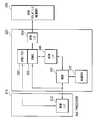
도 2를 참조하면, 상기 시스템(200)은 SoC 프로세서(210), 메모리 장치(220) 및 비휘발성 메모리(230)를 포함한다. 상기 메모리 장치(220)은 메모리(222)와 주변회로를 포함하고 있다. 상기 메모리 장치(220)는 상기 SoC 프로세서(210) 및 상기 비휘발성 메모리(230)과 연결되어 있다. 따라서 종래에는 상기 메모리 장치(220)와 상기 비휘발성 메모리(230) 간의 데이터 송수신은 상기 SoC 프로세서(210)를 경유하였으나, 본 발명에서는 상기 SoC 프로세서(210)를 경유하지 않고, 상기 메모리 장치(220)와 상기 비휘발성 메모리(230) 간의 데이터 송수신을 할 수 있다.Referring to FIG. 2, the system 200 includes an
본 발명의 일 실시예에 따르면, 상기 SoC 프로세서(210)는 메모리 인터페이스 회로(212)를 포함하며, 메모리 인터페이스 회로(212)를 통하여 상기 메모리 장치(220)과 연결된다. 또한 상기 메모리 장치(220)은 비휘발성 메모리 인터페이스 회로(224)를 포함하며, 비휘발성 메모리 인터페이스 회로(224)를 통하여 상기 비휘발성 메모리(230)과 연결된다. 따라서, 상기 메모리 장치(220)과 상기 비휘발성 메모리(230)과의 데이터 송수신시, 상기 프로세서(210)을 거치지 않게 되어, 상기 프로세서(210)의 동작이 지연되지 않고, 데이터 송수신시 상기 프로세서(210)가 동작되지 않음으로써, 전원소모를 줄일 수 있다. 도면에 도시된 디렉트 메모리 엑세스 제어기 (Direct Memory Access Controller, "DMAC")(320), 중재기(322), 메모리 인터페이스(340), 및 멀티플렉서(330)은 도 3을 통하여 상세히 설명된다.According to an embodiment of the present invention, the SoC
도 3은 도 2의 메모리 장치를 상세하게 도시한 블록도이다.FIG. 3 is a detailed block diagram illustrating the memory device of FIG. 2.
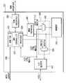
도 3을 참조하면, 상기 메모리 장치(220)는 상기 SoC 프로세서(210) 또는 상기 비휘발성 메모리(230)으로부터 데이터를 수신하여 저장하는 메모리(222), 상기 프로세서(210) 또는 상기 비휘발성 메모리(230)으로부터 상기 메모리(222)의 접근을 제어하는 디렉트 메모리 엑세스 제어기 ("DMAC")(320)를 포함하되, 상기 프로세서(210)와 상기 DMAC(320), 상기 프로세서(210)와 상기 메모리(222), 및 상기 DMAC(320)와 상기 메모리(222) 사이의 데이터 송수신을 조절하기 위하여 상기 DMAC(320)는 중재기(Arbiter)(322)를 포함하고 있다.Referring to FIG. 3, the
본 발명의 일실시예에 따르면, 상기 중재기(322)는 상기 DMAC(320)에 포함되어 설명하나, 상기 DMAC(320)에 분리되어 구성될 수도 있다.According to one embodiment of the invention, the
본 발명의 일 실시예에 따르면, 상기 메모리(222)는 디램(Dynamic Random Access Memory, "DRAM")이며, 싱크로너스(Synchronous) DRAM이 주로 사용될 수 있다.According to an embodiment of the present invention, the
또한 상기 메모리 장치(220)은 멀티플렉서(Multiplexer)(330)를 더 포함할 수 있다. 본 발명의 일 실시예에 따르면, 상기 멀티플렉서(330)는 제1 멀티플렉서(332) 및 제2 멀티플렉서(334)를 포함하며, 상기 메모리(222)와 상기 DMAC(320) 사이에 위치하고, 상기 중재기(322)의 명령에 따라 데이터의 전송을 제어한다. 즉, 상기 프로세서(210)의 데이터를 상기 메모리(222)로 전송하기 위해서는, 상기 멀티플렉서(330)는 상기 프로세서(210)에서 생성되는 제1 칩선택 신호(nCS0)에 응답하여, 데이터를 WDATA 라인을 통하여 상기 메모리(222)로 전송한다. 또한, 상기 DMAC(320)의 데이터를 상기 메모리(222)로 전송하기 위해서는, 상기 멀티플렉서(330)은 상기 DMAC(324)에서 생성되는 제3 칩선택 신호(nCS2)에 응답하여, 데이터를 WDATA2 라인을 통하여 상기 메모리(222)에 전송한다.In addition, the
한편, 상기 메모리(222)에 저장된 데이터 또는 상기 DMAC(320)에 저장된 데이터를 상기 프로세서(210)가 읽는 경우에는, 상기 중재기(322)의 제어 동작없이 상기 프로세서(210)의 명령으로 수행된다. 또한, 상기 메모리(222)에 저장된 데이 터를 DMAC(320)이 읽는 경우에도, 상기 중재기(322)의 제어 동작없이 DMAC(320)의 명령에 따라 수행된다.On the other hand, when the
상기 메모리 장치(220)는 상기 멀티플렉서(330)와 상기 DMAC(320)에 사이에 위치하는 메모리 인터페이스(Interface) 회로(340)를 더 포함할 수 있다. 또한, 상기 메모리 장치(220)은 상기 DMAC(320)와 상기 비휘발성 메모리(230)과의 연결을 위한 비휘발성 메모리 인터페이스 회로(224)를 더 포함할 수 있으며, 상기 프로세서(210)와 데이터 입출력을 위한 입출력 버퍼(Buffer) 회로(350)를 더 포함할 수 있다.The
본 발명의 일 실시예에 따르면, 상기 DMAC(320)는 데이터를 저장할 수 있는 레지스터(Register)(또는 버퍼)(324)를 포함하고 있다. 또한 상기 비휘발성 메모리는 NAND 플래쉬 메모리를 포함한다.According to an embodiment of the present invention, the
본 발명의 일 실시예에 따르면, 상기 중재기(322)와 상기 SoC 프로세서(210)의 메모리 인터페이스 회로(212)사이에는 서로 명령을 송수신할 수 있는 신호선(326)이 존재한다. 이 신호선(326)을 통하여 상기 프로세서(210)는 상기 메모리(222)의 접근(Access) 필요시 리퀘스트 신호(nREQ)를 상기 중재기(322)에 송신하고, 상기 리퀘스트 신호(nREQ)에 따라 상기 중재기(322)는 상기 메모리(222)의 접근 허가시 허가신호(nGRANT)를 상기 프로세서(210)에 송신한다. 상기 중재기(322)의 허가신호(nGRANT)에 따라, 상기 프로세서(210)와 상기 메모리와의 데이터 송수신을 위해 제1 칩선택신호(nCS0) 및 상기 프로세서(210)와 상기 DMAC(320)간 데이터 송수신을 위한 제2 칩선택신호(nCS1) 신호를 발생한다.According to one embodiment of the invention, there is a
한편, 상기 DMAC(320)는 상기 비휘발성 메모리(230)으로부터 데이터를 수신하고, 상기 레지스터(324)에 저장한 후, 상기 메모리(222)에 송신한다. 이 경우, 만약 상기 프로세서(210)가 데이터를 상기 메모리(222)에 송신하고 있는 경우, 서로 충돌하게 되는데, 이를 상기 중재기(322)는 서로 충돌이 발생하지 않도록 조정한다. 이때, 상기 중재기(322)에서 허가신호(nGRANT)를 비활성화시키고, 상기 DMAC(322)는 제3 칩선택신호(nCS3)를 발생시키면, 상기 DMAC(320)와 상기 메모리와의 데이터 송수신이 발생한다.Meanwhile, the
이하, 본 발명에 따른 데이터의 전송 과정을 예를 들어 다음 4가지 경우에 따라 상세하게 설명한다.Hereinafter, the data transmission process according to the present invention will be described in detail according to the following four cases.
도 4는 본 발명의 일 실시예에 따른 프로세서(210)와 메모리 장치(220) 및 비휘발성 메모리(230) 사이의 데이터 송수신을 설명하기 위한 개략적인 블록도이다.4 is a schematic block diagram illustrating data transmission and reception between a
첫째, 상기 프로세서(210)의 메모리 인터페이스 회로(212)와 상기 메모리 장치(220) 내부의 메모리(222)간의 제1 경로(1)를 통한 데이터 송수신시, 상기 중재기(322)로부터 허가(nGRANT 액티브 상태)를 획득한 후, 상기 제1 선택 신호선(nCS0 신호선) / 제1 콘트롤 신호선 (CTRL 신호선) / 제1 쓰기데이터 신호선(WDATA 신호선) / 제1 읽기데이터 신호선 (RDATA0 신호선)을 사용하여 송수신이 이루어진다. (이하 "1번 전송") 여기서, 프로세서(210)에서 메모리(222)로의 데이터 전송은 WDATA 신호선을 통하여 이루어지며, 메모리(222)에서 프로세서(210)로의 데이터 전송은 RDATA0 신호선을 통하여 이루어진다.First, when the data is transmitted / received through the
둘째, 상기 프로세서(210)의 메모리 인터페이스 회로(212)와 상기 메모리 장치(220) 내부의 DMAC 레지스터(324)간의 제2 경로(2)를 통한 데이터 송수신시, 상기 중재기(322)로부터 허가를 획득한 후, 제2 선택 신호선(nCS1 신호선) / 제1 콘트롤 신호선 (CTRL 신호선) / 제1 쓰기데이터 신호선(WDATA 신호선) / 제2 읽기데이터 신호선 (RDATA1 신호선) 을 사용하여 송수신이 이루어진다. (이하 "2번 전송") 여기서, DAMA 레지서터(324)에서 프로세서(210)으로의 데이터 전송은 RDATA1 신호선을 통하여 이루어진다.Second, when data is transmitted / received through the
셋째, 상기 DMAC(320)와 상기 비휘발성 메모리(230) 간의 제3 경로(3)를 통한 데이터 송수신시, 상기 DMAC(320)의 내부 레지스터(324)에 저장된 데이터는 상기 NVM 인터페이스 회로(224)를 경유하여 상기 비휘발성 메모리(230)에 송신되고, 상기 비휘발성 메모리(230)의 데이터는 상기 NVM 인터페이스 회로(224)를 경유하여 상기 DMAC(320)의 내부 레지스터(324)에 전송된다. 이때 상기 중재기(322)의 제어를 받지 않는다. (이하 "3번 전송")Third, when data is transmitted and received through the
넷째, 상기 중재기(322)의 허가(nGRANT 액티브 상태)가 있을 때만, 상기 DMAC(320)에서 메모리 인터페이스 회로(340)을 경유하여 상기 메모리(222)간의 데이터 송수신이 이루어진다. 상기 메모리(222)와 상기 DMAC(320) 간의 데이터 송수신시, 메모리 인터페이스 회로(340)을 경유한다. 이 때 제3 선택 신호선(nCS2 신호선) / 제3 콘트롤 신호선 (CTRL2 신호선) / 제3 쓰기데이터 신호선(WDATA2 신호선) / 제1 읽기데이터 신호선 (RDATA0 신호선)이 사용된다. (이하 "4번 전송") 여기서, DMAC 레지스터(324)에서 메모리(222)로의 데이터 전송은 WDATA2 신호선을 통하여 이루어지며, 메모리(222)에서 DMAC 레지스터(324)로의 데이터 전송은 RDATA0 신호선을 통하여 이루어진다.Fourth, data is transmitted and received between the
이하, 상기 "3번 및 4번 전송"경우를 타이밍도를 통하여 상세히 설명한다.Hereinafter, the "
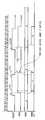
도 5는 본 발명의 일 실시예에 따른 비휘발성 메모리와 메모리 장치간에 데이터전송을 도시한 타이밍도이다.5 is a timing diagram illustrating data transfer between a nonvolatile memory and a memory device according to an embodiment of the present invention.
도 5을 참조하면, "NAND R/B" 축은 비휘발성 메모리(230)가 래디/비지(Ready/Busy)를 나타낸다. NAND R/B가 하이(high)이면 불휘발성 메모리(230)가 데이터 전송이 가능한 상태(ready)이고, NAND R/B가 로우(low)이면 불휘발성 메모리(230)가 데이터 전송이 불가능한 상태(busy)이다. "NAND 10" 축은 비휘발성 메모리(230) 신호선을 의미하고, "SDRAM DQ" 축은 상기 메모리(222)의 데이터 신호선을 의미한다. "NAND 10" 축의 "A"또는 "B"는 상기 DMAC(320)의 내부 레지스터(324)의 버퍼만큼의 데이터 전송을 의미한다. 본 발명에의 일 실시예에 따르면, 우선 비휘발성 메모리(230)가 래디되면 명령과 주소에 해당되는 비휘발성 메모리(230)의 데이터가 상기 DMAC(320)의 내부 레지스터(324)의 버퍼로 이동된다. 상기 DMAC(320)의 내부 레지스터(324)의 버퍼는 예를 들어, 2개 사용하며, 데이터가 비휘발성 메모리(230)에서 DMAC(320)의 "B"버퍼로 로드(Load)되는 동안(T1 구간), "A" 버퍼의 데이터는 메모리(222)로 전송된다. 마찬가지로 데이터가 비휘발성 메모리(230)에서 DMAC(320)의 "A" 버퍼로 로드(load)되는 동안 (T2 구간), "B" 버퍼 데이터는 메모리(222)로 전송된다. 예를 들어, A 및 B버퍼의 크기는 각각 약 16 바이트이다. 또한, 상기 메모리(222)와 상기 DMAC(320)는 상기 메모리 장치(220) 내부에 존재하기 때문에 데이터를 읽을 수 있는 속도가 매우 빠르다. 따라서, "SDRAM DQ" 축은 데이터를 상기 DMAC(320)의 레지스터 버퍼(324)에서 읽는 속도보다 훨씬 빠르게 된다.Referring to FIG. 5, the "NAND R / B" axis represents the read / busy of the
이하, 상기 프로세서(210)와 DMAC(320)이 서로 상기 메모리(222)를 엑세스(Access)시 충돌을 방지하기 위한 중재(Arbitration)하는 방법을 설명한다.Hereinafter, a description will be given of a method in which the
도 6은 본 발명의 일 실시예에 따른 "1번 전송"이 일어나고, "3번 및 4번 전송"이 일어날 때의 중재 상황을 설명하기 위한 타이밍도이다.FIG. 6 is a timing diagram illustrating an arbitration situation when "transmission once" and "transmission three and fourth" occur according to an embodiment of the present invention.
도 6을 참조하면, 프로세서(210)는 메모리(222)를 엑세스하기 위하여 리궤스트(nREQ) 신호를 활성화("low")시키면, 중재기(322)는 그랜트(nGRANT) 신호를 상기 프로세서(210)에 보낸다. 따라서, 우선적으로 상기 프로세서(210)는 상기 메모리(222)를 엑세스한다. 프로세서(210)가 메모리(222)를 엑세스하는 동안 (processpr access 1)에는 비휘발성 메모리(230)에서는 DMAC(320)의 레지스터 버퍼(324)에 데이터(A, B)를 전송하고 있다. 도 6에 도시된 바와 같이, 본 발명의 일실시예에 따르면, 일단 프로세서(210)가 메모리(222)를 엑세스 하는 동안 (processor access 1)에도 중재기(322)는 디렉트 메모리 엑세스 제어기(320)로 전송될 수 있도록 nGRANT 신호를 비활성화(high) 시킨다. 만약, nREQ신호가 "활성"("low")에서 "비활성"("high")로 바뀌면, 1 클럭 후에 DMAC(320)의 레지스터 버퍼에 저장된 비휘발성 메모리 데이터("A" , "B")는 상기 메모리(222)로 전송된다. 본 발명의 일실시예에 따르면, 중재기(322)에서는 DMAC에서 메모리(222)로의 데이터 전송이 끝나기 1 클럭전에 nGRANT를 활성화('low')시킬 수 있다.Referring to FIG. 6, when the
다시 프로세서(210)는 메모리(222)를 엑세스가 필요하면, 리궤스트(nREQ) 신 호를 활성화(Active "low")시키고, 중재기(322)는 활성화된 그랜트(nGRANT) 신호를 상기 프로세서(210)에 보낸다. 이때, t2 시점에서 DMAC(320)의 레지스터(324) 버퍼에서 메모리(222)로의 데이터 전송은 중지되고, 프로세서(210)가 메모리(222)를 엑세스 (processor access 2)하게 된다.When the
도 7은 본 발명의 일 실시예에 따른 "1번 전송"은 일어나지 않고, "3번 및 4번 전송" 이 일어날 때의 중재 상황을 설명하기 위한 타이밍도이다.FIG. 7 is a timing diagram for describing an arbitration situation when “transmission once” does not occur and “transmit
도 7을 참조하면, 프로세서(210)은 메모리(222)를 엑세스할 필요가 없더라도 리궤스트(nREQ)를 활성화(Active "low")시켜서(T3 구간), 프로세서(210)에서 메모리(222) 엑세스가 필요할 때 1 클럭의 지연없이 엑세스를 시작할 수 있도록 한다. 도 7에 도시된 바와 같이, 본 발명의 일실시예에 따르면, nGRANT신호는 nREQ 신호가 활성화되기 전에 미리 활성화('low')되어 있다. 즉, 중재기(322)는 프로세서(210)가 사용가능한 상태라면 nREQ 신호가 활성화되지 않더라고, nGRANT 신호를 활성화시킨다. 예를 들면, DMAC(320)로부터 메모리(222) 엑세스를 요청하는 신호인 nREQ신호(미도시)가 중재기(322)에 입력되는 경우, DMAC(320) 및 프로세서(210)가 사용가능한 상태로 판단할 수 있다. 또한, 프로세서(210)가 사용가능한지 여부는 DMAC(320)이 동작중(busy)인지 여부로도 판단할 수 있다.Referring to FIG. 7, even when the
nREQ 신호가 "로우"에서 "하이"로 바뀌면, 1 클럭 후에 DMAC(320)의 레지스터(324) 버퍼에 저장된 비휘발성 메모리 데이터("A")는 상기 메모리(222)로 전송된다. 만약 nREQ 신호가 "하이"에서 "로우"로 바뀌면, DMAC(320)의 레지스터(324) 버퍼에서 메모리(222)로의 데이터 전송은 중지된다(T3구간). 그 결과, T3 구간에서 프로세서(210)가 메모리(222)를 엑세스 가능한 상태가 된다. nREQ 신호가 "로우"에서 "하이"로 바뀌면, 1 클럭후에 DMAC(320)의 레지스터 버퍼에 저장된 비휘발성 메모리 데이터("B")는 상기 메모리(222)로 전송된다.When the nREQ signal changes from " low " to " high ", nonvolatile memory data " A " stored in the
본 발명에 따라, 프로세서(Processor)와 비휘발성 메모리 사이에 위치한 중재기를 포함한 메모리 장치를 사용하여, 전원 소모를 감소시킬 수 있다. 또한, 상기 프로세서, 상기 비휘발성 메모리 및 상기 메모리 장치간의 데이터 전송을 빠르게 할 수 있다.According to the present invention, power consumption can be reduced by using a memory device including an arbiter located between the processor and the nonvolatile memory. In addition, data transfer between the processor, the nonvolatile memory, and the memory device can be accelerated.
상기에서는 본 발명의 바람직한 실시예를 참조하여 설명하였지만, 해당 기술 분야의 숙련된 당업자는 하기의 특허 청구의 범위에 기재된 본 발명의 사상 및 영역으로부터 벗어나지 않는 범위 내에서 본 발명을 다양하게 수정 및 변경시킬 수 있음을 이해할 수 있을 것이다.Although described above with reference to a preferred embodiment of the present invention, those skilled in the art will be variously modified and changed within the scope of the invention without departing from the spirit and scope of the invention described in the claims below I can understand that you can.
Claims (44)
Translated fromKoreanPriority Applications (3)
| Application Number | Priority Date | Filing Date | Title |
|---|---|---|---|
| KR1020040085255AKR100551480B1 (en) | 2004-10-25 | 2004-10-25 | A memory device located between the processor and the nonvolatile memory, a system including the same, and a data transmission / reception method within the system |
| US11/141,091US20060090017A1 (en) | 2004-10-25 | 2005-05-31 | Microprocessor system with memory device including a DMAC, and a bus for DMA transfer of data between memory devices |
| CNA2005101069363ACN1766862A (en) | 2004-10-25 | 2005-09-22 | Microprocessor system for memory devices including memory access controller and bus |
Applications Claiming Priority (1)
| Application Number | Priority Date | Filing Date | Title |
|---|---|---|---|
| KR1020040085255AKR100551480B1 (en) | 2004-10-25 | 2004-10-25 | A memory device located between the processor and the nonvolatile memory, a system including the same, and a data transmission / reception method within the system |
Publications (1)
| Publication Number | Publication Date |
|---|---|
| KR100551480B1true KR100551480B1 (en) | 2006-02-13 |
Family
ID=36207326
Family Applications (1)
| Application Number | Title | Priority Date | Filing Date |
|---|---|---|---|
| KR1020040085255AExpired - Fee RelatedKR100551480B1 (en) | 2004-10-25 | 2004-10-25 | A memory device located between the processor and the nonvolatile memory, a system including the same, and a data transmission / reception method within the system |
Country Status (3)
| Country | Link |
|---|---|
| US (1) | US20060090017A1 (en) |
| KR (1) | KR100551480B1 (en) |
| CN (1) | CN1766862A (en) |
Families Citing this family (26)
| Publication number | Priority date | Publication date | Assignee | Title |
|---|---|---|---|---|
| KR100673013B1 (en)* | 2005-09-21 | 2007-01-24 | 삼성전자주식회사 | Memory controller and data processing system including it |
| FR2901618A1 (en)* | 2006-05-24 | 2007-11-30 | St Microelectronics Sa | DMA CONTROLLER, ON-CHIP SYSTEM COMPRISING SUCH A DMA CONTROLLER, METHOD OF EXCHANGING DATA THROUGH SUCH A DMA CONTROLLER |
| US20080207252A1 (en)* | 2007-02-23 | 2008-08-28 | Magnus Tillgren | Mobile telephone with direct memory access |
| US20080222365A1 (en)* | 2007-03-08 | 2008-09-11 | Staktek Group L.P. | Managed Memory System |
| US8122322B2 (en) | 2007-07-31 | 2012-02-21 | Seagate Technology Llc | System and method of storing reliability data |
| US9201790B2 (en)* | 2007-10-09 | 2015-12-01 | Seagate Technology Llc | System and method of matching data rates |
| US7430584B1 (en)* | 2008-03-12 | 2008-09-30 | Gene Fein | Data forwarding storage |
| US7636761B1 (en)* | 2008-09-29 | 2009-12-22 | Gene Fein | Measurement in data forwarding storage |
| US8458285B2 (en) | 2008-03-20 | 2013-06-04 | Post Dahl Co. Limited Liability Company | Redundant data forwarding storage |
| US7636759B1 (en)* | 2008-09-29 | 2009-12-22 | Gene Fein | Rotating encryption in data forwarding storage |
| US7877456B2 (en)* | 2008-04-08 | 2011-01-25 | Post Dahl Co. Limited Liability Company | Data file forwarding storage and search |
| US8386585B2 (en)* | 2008-04-25 | 2013-02-26 | Tajitshu Transfer Limited Liability Company | Real-time communications over data forwarding framework |
| US8452844B2 (en)* | 2008-05-07 | 2013-05-28 | Tajitshu Transfer Limited Liability Company | Deletion in data file forwarding framework |
| US8599678B2 (en) | 2008-07-10 | 2013-12-03 | Tajitshu Transfer Limited Liability Company | Media delivery in data forwarding storage network |
| US8478823B2 (en) | 2008-09-29 | 2013-07-02 | Tajitshu Transfer Limited Liability Company | Selective data forwarding storage |
| US8352635B2 (en)* | 2008-09-29 | 2013-01-08 | Tajitshu Transfer Limited Liability Company | Geolocation assisted data forwarding storage |
| US8219741B2 (en) | 2008-10-24 | 2012-07-10 | Microsoft Corporation | Hardware and operating system support for persistent memory on a memory bus |
| KR101671334B1 (en)* | 2010-07-27 | 2016-11-02 | 삼성전자주식회사 | Non volatile memory apparatus and data controlling method thereof |
| JP5023208B2 (en)* | 2010-12-17 | 2012-09-12 | 株式会社東芝 | Semiconductor memory device and test method thereof |
| FR2977690B1 (en)* | 2011-07-04 | 2013-08-02 | St Microelectronics Rousset | METHOD FOR INITIALIZING PERIPHERAL ORGAN REGISTERS IN A MICROCONTROLLER |
| CN102591819A (en)* | 2011-12-23 | 2012-07-18 | 西安奇维科技股份有限公司 | Method of using bus switch to control multiprocessor to realize high-speed parallel load |
| CN104932999B (en)* | 2014-03-17 | 2018-02-27 | 联想(北京)有限公司 | A kind of USB mode-changeover device and intelligent terminal |
| US9430393B2 (en)* | 2014-05-26 | 2016-08-30 | Texas Instruments Incorporated | System and method for managing cache |
| CN104598406B (en)* | 2015-02-03 | 2018-02-09 | 杭州士兰控股有限公司 | Expanded function unit and computing device extension system and extended method |
| FR3118528B1 (en)* | 2020-12-28 | 2023-12-01 | Commissariat Energie Atomique | Memory module suitable for implementing calculation functions |
| US20240086346A1 (en)* | 2022-09-08 | 2024-03-14 | Sunrise Memory Corporation | Dynamic random-access memory (dram) configured for block transfers and method thereof |
Citations (7)
| Publication number | Priority date | Publication date | Assignee | Title |
|---|---|---|---|---|
| JPH0244445A (en)* | 1988-08-05 | 1990-02-14 | Sanyo Electric Co Ltd | Data processor |
| US5241661A (en) | 1987-03-27 | 1993-08-31 | International Business Machines Corporation | DMA access arbitration device in which CPU can arbitrate on behalf of attachment having no arbiter |
| KR970049652A (en)* | 1995-12-26 | 1997-07-29 | 정장호 | Bused Arbitration Circuit in Direct Memory Access |
| KR970047757U (en)* | 1995-12-27 | 1997-07-31 | 엘지정보통신주식회사 | Static RAM license arbitration circuit |
| KR20010087646A (en)* | 2000-03-08 | 2001-09-21 | 구자홍 | Apparatus for controlling memory |
| KR20030025018A (en)* | 2001-09-19 | 2003-03-28 | 한국전자통신연구원 | Direct Memory Access(DMA) Controller and control method |
| JP2003162496A (en) | 2001-06-26 | 2003-06-06 | Ricoh Co Ltd | DMA transfer device |
Family Cites Families (13)
| Publication number | Priority date | Publication date | Assignee | Title |
|---|---|---|---|---|
| US5212781A (en)* | 1990-03-21 | 1993-05-18 | Chips And Technologies, Inc. | Secondary cache control for a computer system |
| JPH06162743A (en)* | 1992-11-13 | 1994-06-10 | Sony Corp | Method and device for optical disk reproducing |
| US5671446A (en)* | 1995-03-16 | 1997-09-23 | Apple Computer, Inc. | Method and apparatus for atomically accessing a queue in a memory structure where LIFO is converted to FIFO |
| JPH10133998A (en)* | 1996-11-05 | 1998-05-22 | Canon Inc | Data processing method and recording apparatus using the method |
| JP2001180083A (en)* | 1999-12-24 | 2001-07-03 | Fuji Xerox Co Ltd | Printer |
| US20030046499A1 (en)* | 2001-08-30 | 2003-03-06 | Wen Lin | Integrated drive controller for systems with integrated mass storage |
| US6742058B2 (en)* | 2002-09-27 | 2004-05-25 | Texas Instruments Incorporated | Memory controller having a multiplexer selecting either second set of input signals or converted signals from first set of input signals by a bus mode input |
| US7000092B2 (en)* | 2002-12-12 | 2006-02-14 | Lsi Logic Corporation | Heterogeneous multi-processor reference design |
| JP2004227049A (en)* | 2003-01-20 | 2004-08-12 | Renesas Technology Corp | Data transfer device, semiconductor integrated circuit and microcomputer |
| US7069413B1 (en)* | 2003-01-29 | 2006-06-27 | Vmware, Inc. | Method and system for performing virtual to physical address translations in a virtual machine monitor |
| JP2005115603A (en)* | 2003-10-07 | 2005-04-28 | Hitachi Ltd | Storage device control apparatus and control method thereof |
| JP4405277B2 (en)* | 2004-02-16 | 2010-01-27 | 株式会社日立製作所 | Disk controller |
| US7213082B2 (en)* | 2004-03-29 | 2007-05-01 | Micron Technology, Inc. | Memory hub and method for providing memory sequencing hints |
- 2004
- 2004-10-25KRKR1020040085255Apatent/KR100551480B1/ennot_activeExpired - Fee Related
- 2005
- 2005-05-31USUS11/141,091patent/US20060090017A1/ennot_activeAbandoned
- 2005-09-22CNCNA2005101069363Apatent/CN1766862A/enactivePending
Patent Citations (7)
| Publication number | Priority date | Publication date | Assignee | Title |
|---|---|---|---|---|
| US5241661A (en) | 1987-03-27 | 1993-08-31 | International Business Machines Corporation | DMA access arbitration device in which CPU can arbitrate on behalf of attachment having no arbiter |
| JPH0244445A (en)* | 1988-08-05 | 1990-02-14 | Sanyo Electric Co Ltd | Data processor |
| KR970049652A (en)* | 1995-12-26 | 1997-07-29 | 정장호 | Bused Arbitration Circuit in Direct Memory Access |
| KR970047757U (en)* | 1995-12-27 | 1997-07-31 | 엘지정보통신주식회사 | Static RAM license arbitration circuit |
| KR20010087646A (en)* | 2000-03-08 | 2001-09-21 | 구자홍 | Apparatus for controlling memory |
| JP2003162496A (en) | 2001-06-26 | 2003-06-06 | Ricoh Co Ltd | DMA transfer device |
| KR20030025018A (en)* | 2001-09-19 | 2003-03-28 | 한국전자통신연구원 | Direct Memory Access(DMA) Controller and control method |
Also Published As
| Publication number | Publication date |
|---|---|
| US20060090017A1 (en) | 2006-04-27 |
| CN1766862A (en) | 2006-05-03 |
Similar Documents
| Publication | Publication Date | Title |
|---|---|---|
| KR100551480B1 (en) | A memory device located between the processor and the nonvolatile memory, a system including the same, and a data transmission / reception method within the system | |
| US4737932A (en) | Processor | |
| US7752373B2 (en) | System and method for controlling memory operations | |
| US8086767B2 (en) | Pin multiplexing | |
| US8707002B2 (en) | Control apparatus | |
| US20090089517A1 (en) | Memory control device and semiconductor processing apparatus | |
| US8433835B2 (en) | Information processing system and control method thereof | |
| US7162556B2 (en) | Matrix type bus connection system and power reduction method therefor | |
| US6782463B2 (en) | Shared memory array | |
| JPH06231074A (en) | Multiple access system for system bus | |
| JP4902640B2 (en) | Integrated circuit and integrated circuit system | |
| US7600065B2 (en) | Arbitration scheme for shared memory device | |
| JP4869713B2 (en) | Multi-chip package device | |
| US6775718B2 (en) | DMA control system enabling flyby transfer to synchronous memory | |
| KR101022473B1 (en) | Method and apparatus for memory bank interleaving in multilayer bus system | |
| KR20050079862A (en) | Dual port memory device having protection signal | |
| US8244987B2 (en) | Memory access device including multiple processors | |
| US6829692B2 (en) | System and method for providing data to multi-function memory | |
| KR100964154B1 (en) | How to control shared bank access of dual port memory and dual port memory | |
| JP4843216B2 (en) | Memory control device | |
| KR100441996B1 (en) | Direct Memory Access(DMA) Controller and control method | |
| CN107025190B (en) | System and how to operate it | |
| US20080228961A1 (en) | System including virtual dma and driving method thereof | |
| KR100217743B1 (en) | Shared memory connection device and its connection method | |
| JPH09198298A (en) | Memory controller |
Legal Events
| Date | Code | Title | Description |
|---|---|---|---|
| A201 | Request for examination | ||
| PA0109 | Patent application | St.27 status event code:A-0-1-A10-A12-nap-PA0109 | |
| PA0201 | Request for examination | St.27 status event code:A-1-2-D10-D11-exm-PA0201 | |
| PN2301 | Change of applicant | St.27 status event code:A-3-3-R10-R13-asn-PN2301 St.27 status event code:A-3-3-R10-R11-asn-PN2301 | |
| PN2301 | Change of applicant | St.27 status event code:A-3-3-R10-R13-asn-PN2301 St.27 status event code:A-3-3-R10-R11-asn-PN2301 | |
| D13-X000 | Search requested | St.27 status event code:A-1-2-D10-D13-srh-X000 | |
| D14-X000 | Search report completed | St.27 status event code:A-1-2-D10-D14-srh-X000 | |
| E701 | Decision to grant or registration of patent right | ||
| PE0701 | Decision of registration | St.27 status event code:A-1-2-D10-D22-exm-PE0701 | |
| GRNT | Written decision to grant | ||
| PR0701 | Registration of establishment | St.27 status event code:A-2-4-F10-F11-exm-PR0701 | |
| PR1002 | Payment of registration fee | St.27 status event code:A-2-2-U10-U11-oth-PR1002 Fee payment year number:1 | |
| PG1601 | Publication of registration | St.27 status event code:A-4-4-Q10-Q13-nap-PG1601 | |
| PR1001 | Payment of annual fee | St.27 status event code:A-4-4-U10-U11-oth-PR1001 Fee payment year number:4 | |
| FPAY | Annual fee payment | Payment date:20100114 Year of fee payment:5 | |
| PR1001 | Payment of annual fee | St.27 status event code:A-4-4-U10-U11-oth-PR1001 Fee payment year number:5 | |
| LAPS | Lapse due to unpaid annual fee | ||
| PC1903 | Unpaid annual fee | St.27 status event code:A-4-4-U10-U13-oth-PC1903 Not in force date:20110207 Payment event data comment text:Termination Category : DEFAULT_OF_REGISTRATION_FEE | |
| PC1903 | Unpaid annual fee | St.27 status event code:N-4-6-H10-H13-oth-PC1903 Ip right cessation event data comment text:Termination Category : DEFAULT_OF_REGISTRATION_FEE Not in force date:20110207 | |
| R18-X000 | Changes to party contact information recorded | St.27 status event code:A-5-5-R10-R18-oth-X000 |