KR100551474B1 - Open Drain Driver and its Current Driving Method for Minimizing Substrate Noise - Google Patents
Open Drain Driver and its Current Driving Method for Minimizing Substrate NoiseDownload PDFInfo
- Publication number
- KR100551474B1 KR100551474B1KR1020040056676AKR20040056676AKR100551474B1KR 100551474 B1KR100551474 B1KR 100551474B1KR 1020040056676 AKR1020040056676 AKR 1020040056676AKR 20040056676 AKR20040056676 AKR 20040056676AKR 100551474 B1KR100551474 B1KR 100551474B1
- Authority
- KR
- South Korea
- Prior art keywords
- pull
- switch unit
- current
- node
- switching
- Prior art date
- Legal status (The legal status is an assumption and is not a legal conclusion. Google has not performed a legal analysis and makes no representation as to the accuracy of the status listed.)
- Expired - Fee Related
Links
Images


Classifications
- H—ELECTRICITY
- H03—ELECTRONIC CIRCUITRY
- H03K—PULSE TECHNIQUE
- H03K19/00—Logic circuits, i.e. having at least two inputs acting on one output; Inverting circuits
- H03K19/0008—Arrangements for reducing power consumption
- H03K19/0013—Arrangements for reducing power consumption in field effect transistor circuits
- H—ELECTRICITY
- H03—ELECTRONIC CIRCUITRY
- H03K—PULSE TECHNIQUE
- H03K17/00—Electronic switching or gating, i.e. not by contact-making and –breaking
- H03K17/16—Modifications for eliminating interference voltages or currents
- H—ELECTRICITY
- H03—ELECTRONIC CIRCUITRY
- H03K—PULSE TECHNIQUE
- H03K19/00—Logic circuits, i.e. having at least two inputs acting on one output; Inverting circuits
- H03K19/0175—Coupling arrangements; Interface arrangements
- H03K19/0185—Coupling arrangements; Interface arrangements using field effect transistors only
- H03K19/018507—Interface arrangements
- H03K19/018521—Interface arrangements of complementary type, e.g. CMOS
Landscapes
- Engineering & Computer Science (AREA)
- Computer Hardware Design (AREA)
- Physics & Mathematics (AREA)
- Computing Systems (AREA)
- General Engineering & Computer Science (AREA)
- Mathematical Physics (AREA)
- Electronic Switches (AREA)
- Logic Circuits (AREA)
Abstract
Translated fromKoreanDescription
Translated fromKorean도 1은 종래 기술에 따른 3가지 방식의 오픈 드레인 드라이버의 회로도이다.1 is a circuit diagram of three types of open drain drivers according to the prior art.
도 2는 도 1에 도시된 3가지 오픈 드레인 드라이버의 시뮬레이션 파형도이다. FIG. 2 is a simulation waveform diagram of the three open drain drivers shown in FIG. 1.
도 3a는 종래 기술에 따른 제1 변형 오픈 드레인 드라이버의 회로도이다. 3A is a circuit diagram of a first modified open drain driver according to the prior art.
도 3b는 종래 기술에 따른 제2 변형 오픈 드레인 드라이버의 회로도이다.3B is a circuit diagram of a second modified open drain driver according to the prior art.
도 3c는 종래 기술에 따른 제3 변형 오픈 드레인 드라이버의 회로도이다.3C is a circuit diagram of a third modified open drain driver according to the prior art.
도 3d는 종래 기술에 따른 제4 변형 오픈 드레인 드라이버의 회로도이다.3D is a circuit diagram of a fourth modified open drain driver according to the prior art.
도 4는 본 발명의 일실시예에 따른 오픈 드레인 드라이버의 회로도이다. 4 is a circuit diagram of an open drain driver according to an embodiment of the present invention.
도 5는 도 4에 도시된 전류공급부의 다른 구현예의 회로도이다.FIG. 5 is a circuit diagram of another embodiment of the current supply unit shown in FIG. 4.
도 6은 본 발명의 다른 실시예에 따른 오픈 드레인 드라이버의 회로도이다.6 is a circuit diagram of an open drain driver according to another exemplary embodiment of the present invention.
도 7은 종래 기술과 비교한 도 4에 도시된 오픈 드레인 드라이버의 시뮬레이션 파형도이다.7 is a simulated waveform diagram of the open drain driver shown in FIG. 4 compared to the prior art.
도 8은 종래기술 및 도 4에 도시된 오픈 드레인 드라이버의 출력 단자에 패키지 모델을 접속시킨 경우의 시뮬레이션 파형도이다.8 is a simulation waveform diagram when the package model is connected to the output terminal of the prior art and the open drain driver shown in FIG.
도 9는 도 8과 같은 경우에 접지전위에 흐르는 전류를 측정한 시뮬레이션 파형도이다.FIG. 9 is a simulation waveform diagram of measuring a current flowing in the ground potential in the case of FIG. 8.
도 10은 본 발명의 전류 구동회로를 이용하여 구현한 차지 펌프의 회로도이다.10 is a circuit diagram of a charge pump implemented using the current drive circuit of the present invention.
* 도면의 주요부분에 대한 부호의 설명 *Explanation of symbols on the main parts of the drawings
410 : 전류원420 : 전류 공급부410: current source 420: current supply
430 : 제1 풀다운 스위치부440 : 제1 풀업 스위치부430: first pull-down switch unit 440: first pull-up switch unit
450 : 제2 풀다운 스위치부460 : 제2 풀업 스위치부450: second pull-down switch unit 460: second pull-up switch unit
본 발명은 인터페이스 회로 분야에서 전류 구동 방식에 주로 사용되는 전류 드라이버 기술에 대한 것으로 특히 CMOS 오픈 드레인 드라이버에 관한 것이다. 출력 단자로 일정한 전류를 내보내는 것을 선택할 수 있게 해주는 회로는 PLL(Phase Locked Loop)의 차지 펌프(charge pump)에서부터 DAC(Digital-to-Analog Converter), 전류 구동 인터페이스(current driving interface)방식에 이르기까지 여러 곳에 광범위하게 사용된다. 그 중 대표적인 방식으로는 도 1에 도시된 3가지가 있다. 도 1은 종래 기술에 따른 3가지 오픈 드레인 드라이버의 회로도이다. 도 1을 참조하면 먼저 게이트 스위치 방식은 출력 엔모스의 Vgs값의 변동이 너무 크며 드레인 스위치 방식은 전류원 양단간 전압의 급격한 변화에 의한 전류 스파이크(current spike)현상으로 적절하지 않아 주로 소스 스위치 방식이 사용된다. 도 2는 도 1에 도시된 3가지 오픈 드레인 드라이버의 시뮬레이션 파형도이다. 도 2를 참조하면 게이트 스위치 방식은 입력 신호의 변화에 출력 단자의 전류가 잘 따라오지 못하며, 드레인 스위치 방식은 스파이크가 생기는 것을 알 수 있다. 소스 스위치 방식의 경우에는 이러한 문제점을 잘 해결해 주고 있다.BACKGROUND OF THE INVENTION 1. Field of the Invention [0001] The present invention relates to current driver technology mainly used in current driving schemes in the field of interface circuits, and more particularly to CMOS open drain drivers. Circuitry that allows the selection of constant current output to the output terminals ranges from the charge pump of a phase-locked loop (PLL) to digital-to-analog converters (DACs) and current driving interfaces. Widely used in many places. There are three representative methods among them. 1 is a circuit diagram of three open drain drivers according to the prior art. Referring to FIG. 1, first, the gate switch method has a large variation in the Vgs value of the output NMOS, and the drain switch method is not appropriate as a current spike phenomenon caused by a sudden change in voltage between the current source. do. FIG. 2 is a simulation waveform diagram of the three open drain drivers shown in FIG. 1. Referring to FIG. 2, it can be seen that the gate switch method does not follow the current of the output terminal well with the change of the input signal, and the drain switch method has a spike. The source switch method solves this problem well.
그런데 소스 스위치 방식에도 문제가 남아 있다. 온/오프 동작시 스위치와 전류원 사이의 노드가 늦게 반응하여 출력 전류의 상승 시간과 하강 시간이 길어져 전체 시스템 마진을 줄이는 결과를 초래한다. 이를 막기 위하여 도 1에 도시된 소스 스위치 방식의 오픈 드레인 드라이버는 몇 가지 변형을 가진다.However, the problem remains with the source switch method. During on / off operation, the node between the switch and the current source reacts late, resulting in longer rise and fall times of the output current, resulting in lower overall system margins. In order to prevent this, the source switch type open drain driver shown in FIG. 1 has some modifications.
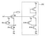
도 3a는 종래 기술에 따른 제1 변형 오픈 드레인 드라이버의 회로도이다. 도 3a를 참조하면 도 1에 도시된 소스 스위치 방식의 오픈 드레인 드라이버에 비하여 도 3a에 도시된 오픈 드레인 드라이버는 입력 신호(din)가 반복적인 '하이', '로우'로 인가될 때 기준전위(ref)에 생기는 전하를 공급 및 흡수하여 기준전위(ref)가 스위칭시에 변동이 없게 하여 일정한 전류가 공급되도록 하는 회로이다. 도 3a에 도시된 오픈 드레인 드라이버는 전류원(310), 전류공급부(320), 제1 풀다운 트랜지스터(M2), 및 제2 풀다운 트랜지스터(M6)를 포함한다. 전류원(310)은 출력단자 및 제1 노드(n1)사이에 연결되어 기준전위(ref)에 따라 제1 기준전류를 공급한다. 제1 풀다운 트랜지스터(M2)는 제1 노드(n1)와 접지전위(Vss)사이에 접속되어 입력 신호(din)에 따라 스위칭 동작을 한다. 따라서 전류원(310) 및 제1 풀다운 트랜지 스터(M2)는 도 1에 도시된 소스 스위치 방식의 오픈 드레인 드라이버에 해당하며 엔모스 트랜지스터(M1)를 이용하여 전류원(310)을 구현한 것이다. 전류공급부(320)는 다이오드 연결된 피모스 트랜지스터(M9) 및 엔모스 트랜지스터(M5)를 포함한다. 엔모스 트랜지스터(M5)는 전류원(310)을 구현하는 엔모스 트랜지스터(M1)와 대응되어 입력 신호(din)에 따른 스위칭 동작에도 불구하고 기준전위(ref)를 일정하게 유지하도록 한다. 제2 풀다운 트랜지스터(M6)는 제1 풀다운 트랜지스터(M2)에 대응하여 제1 풀다운 트랜지스터(M2)와 반대로 스위칭 동작을 하여 엔모스 트랜지스터(M1)와 엔모스 트랜지스터(M5)가 상호 보완적으로 동작하여 기준전위(ref)가 흔들리지 않도록 한다.3A is a circuit diagram of a first modified open drain driver according to the prior art. Referring to FIG. 3A, the open-drain driver shown in FIG. 3A has a reference potential when the input signal din is repeatedly applied to 'high' and 'low' as compared to the open-drain driver of the source switch method shown in FIG. 1. It is a circuit for supplying and absorbing charges generated in ref) so that a reference current ref does not change during switching so that a constant current is supplied. The open drain driver illustrated in FIG. 3A includes a
도 3b는 종래 기술에 따른 제2 변형 오픈 드레인 드라이버의 회로도이다. 도 3b에 도시된 오픈 드레인 드라이버는 도 3a에 도시된 오픈 드레인 드라이버에서 입력 신호(din)가 '로우'일 때 제1 노드(n1)의 전압이 상승하여 전류원에 해당하는 엔모스 트랜지스터(M1)의 Vgs가 Vth보다 낮아질 때까지 엔모스 트랜지스터(M1)가 온 상태여서 출력 단자에서 흐르는 전류의 하강 시간이 길어지게 되는 점을 보완하기 위한 회로이다. 따라서 도 3b에 도시된 오픈 드레인 드라이버는 별도의 풀업 피모스 트랜지스터(M4)를 두어 입력신호(din)가 '로우'일 때 제1 노드(n1)의 전위를 빨리 끌어올리도록 한 회로이다. 따라서 입력 신호(din)가 '로우'일 때 제1 노드(n1)의 전압이 전원전압(VDD)까지 끌어올려져서 엔모스 트랜지스터(M1)가 빨리 오프되게 된다. 도 3b에서도 대칭적인 회로(372)를 기준전위(ref)에 연결하여 입력신호(din)의 스위칭에 따른 기준전위(ref)의 영향을 최소화하고자 한 것을 알 수 있다.3B is a circuit diagram of a second modified open drain driver according to the prior art. In the open drain driver illustrated in FIG. 3B, when the input signal din is 'low' in the open drain driver illustrated in FIG. 3A, the voltage of the first node n1 is increased so that the NMOS transistor M1 corresponds to a current source. The NMOS transistor M1 is turned on until Vgs becomes lower than Vth, and thus the fall time of the current flowing through the output terminal becomes long. Accordingly, the open drain driver illustrated in FIG. 3B is a circuit in which a separate pull-up PMOS transistor M4 is provided to quickly raise the potential of the first node n1 when the input signal din is 'low'. Therefore, when the input signal din is 'low', the voltage of the first node n1 is pulled up to the power supply voltage VDD so that the NMOS transistor M1 is turned off quickly. In FIG. 3B, the
도 3c는 종래 기술에 따른 제3 변형 오픈 드레인 드라이버의 회로도이다. 도 3c의 오픈 드레인 드라이버는 도 3b에 도시된 그것과 유사하나 피모스 트랜지스터 대신에 엔모스 트랜지스터(M3)를 풀업 트랜지스터로 사용한 것을 알 수 있다. 따라서 제1 노드(n1)를 전원전압(VDD)까지 끌어올리는 것이 아니라 전원전압(VDD)에서 엔모스 트랜지스터(M3)의 문턱전압(Vth)을 뺀 전압만큼만 끌어올림으로서 입력신호(din)가 '하이'가 될 때 반응속도를 향상시키기 위한 회로이다. 이 경우에도 대칭적인 회로(373)를 기준전위(ref)에 연결하여 입력신호(din)의 스위칭에 따른 기준전위(ref)의 영향을 최소화하고자 한 것을 알 수 있다.3C is a circuit diagram of a third modified open drain driver according to the prior art. The open drain driver of FIG. 3C is similar to that shown in FIG. 3B but it can be seen that the NMOS transistor M3 is used as a pull-up transistor instead of the PMOS transistor. Therefore, instead of pulling up the first node n1 to the power supply voltage VDD, the input signal din is pulled up by only the voltage obtained by subtracting the threshold voltage Vth of the NMOS transistor M3 from the power supply voltage VDD. It is a circuit to improve the reaction speed when high. Also in this case, it can be seen that the
도 3d는 종래 기술에 따른 제4 변형 오픈 드레인 드라이버의 회로도이다. 도 3d는 연산 증폭기를 사용하여 제1 및 제2 노드(n1, n2)를 기준전위(ref)만큼만 끌어올려서 전류원에 해당하는 엔모스 트랜지스터들(M1, M5)이 빨리 꺼지도록 한다.3D is a circuit diagram of a fourth modified open drain driver according to the prior art. In FIG. 3D, the NMOS transistors M1 and M5 corresponding to the current source are turned off quickly by raising the first and second nodes n1 and n2 by only the reference potential ref using an operational amplifier.
이러한 변형회로들의 문제점은, 먼저 도 3a에 도시된 오픈 드레인 드라이버는 전류의 하강 시간이 길다는 문제점이 있고, 도 3d에 도시된 오픈 드레인 드라이버는 연산 증폭기를 구비하여야 하기 때문에 칩 면적이 커지고 소비전력이 커지며 반응속도가 느리다는 문제점이 있다. 또한, 도 3b 및 도 3c에 도시된 오픈 드레인 드라이버는 풀업 트랜지스터 및 풀다운 트랜지스터가 동시에 전류를 흘리는 경우가 있어서 문제가 된다. 이를 좀 더 자세히 살펴보면 도 3b에 도시된 오픈 드레인 드라이버는 풀업 트랜지스터(M4)가 피모스 트랜지스터이기 때문에 풀다운 트랜지스터(M2)보다 반응이 느리고 따라서 입력 신호(din)가 '로우'에서 '하이'로 갈 때 풀다운 트랜지스터(M2)가 온 된 이후에도 풀업 트랜지스터(M4)가 오프 되지 않는 타이밍이 있어 그 동안 큰 전류를 접지전위로 흘리게 된다. 도 3c에 도시된 오픈 드레인 드라이버는 풀업 트랜지스터(M3) 및 풀다운 트랜지스터(M4)가 모두 엔모스 트랜지스터이나 실제로 풀업 트랜지스터(M3) 및 풀다운 트랜지스터(M4)에는 반응시간의 차이가 있게 된다. 만약 풀업 트랜지스터(M3)의 반응속도가 풀다운 트랜지스터(M2)보다 느리다면 도 3b의 경우와 같은 문제점이 있을 것이다. 만약 풀업 트랜지스터(M3)의 반응속도가 풀다운 트랜지스터(M2)보다 빠르다면 입력 신호(din)가 '하이'에서 '로우'로 갈 때 풀다운 트랜지스터(M2)가 채 온 되지 않은 동안 풀업 트랜지스터(M1)가 오프 되는 타이밍이 있어 그 동안 큰 전류를 접지전위로 흘리게 된다. 따라서 전원전압(VDD)에서 접지전위로 쇼트 전류 경로(short current path)가 생겨 전류가 갑자기 접지전위로 흘러 기판 잡음을 야기하며 소비전력이 커지게 되는 문제점이 있다.The problem with these modified circuits is that the open drain driver shown in FIG. 3A has a long fall time of the current, and the open drain driver shown in FIG. 3D has to have an operational amplifier. Has a problem that the reaction rate is large. In addition, the open-drain driver shown in FIGS. 3B and 3C is a problem because the pull-up transistor and the pull-down transistor simultaneously flow current. In more detail, the open-drain driver shown in FIG. 3B has a slower response than the pull-down transistor M2 because the pull-up transistor M4 is a PMOS transistor, and thus the input signal din goes from 'low' to 'high'. At this time, even after the pull-down transistor M2 is turned on, there is a timing in which the pull-up transistor M4 is not turned off, so that a large current flows to the ground potential. In the open-drain driver shown in FIG. 3C, both the pull-up transistor M3 and the pull-down transistor M4 are NMOS transistors, but there is a difference in response time between the pull-up transistor M3 and the pull-down transistor M4. If the response speed of the pull-up transistor M3 is slower than that of the pull-down transistor M2, there will be the same problem as that of FIG. 3B. If the response speed of the pull-up transistor M3 is faster than that of the pull-down transistor M2, the pull-up transistor M1 is not turned on when the input signal din goes from 'high' to 'low'. There is a timing to turn off so that a large current flows to ground potential. Therefore, a short current path occurs from the power supply voltage VDD to the ground potential, and the current suddenly flows to the ground potential, causing substrate noise and increasing power consumption.
상기와 같은 문제점을 해결하기 위해서 본 발명의 목적은 풀다운 스위치부보다 온 되는 속도는 느리고 오프 되는 속도는 빠른 풀업 스위치부를 포함하는 오픈 드레인 드라이버를 제공하는데 있다. In order to solve the above problems, an object of the present invention is to provide an open-drain driver including a pull-up switch unit is slower than the pull-down switch unit, the speed is turned off faster.
본 발명의 또 다른 목적은 풀다운 스위칭 단계의 스위칭 동작보다 온 되는 속도는 느리고 오프 되는 속도는 빠르게 스위칭 동작을 하는 풀업 스위칭 단계를 포함하는 전류 구동방법을 제공하는데 있다. It is still another object of the present invention to provide a current driving method including a pull-up switching step in which a speed at which an on speed is slower and a speed at which an off speed is faster than a switching operation in a pull-down switching step.
상기 목적을 달성하기 위한 오픈 드레인 드라이버는, 제1 노드와 출력 단자 사이에 연결되어 기준 전류를 공급하는 전류원, 제1 노드와 제1 전원전압 사이에 연결되어 입력 신호에 따라 스위칭을 하는 풀다운 스위치부, 및 제2 전원전압과 제1 노드 사이에 연결되며 풀다운 스위치부와 반대로 스위칭을 함에 있어 풀다운 스위치부보다 온 되는 속도는 느리고 오프되는 속도는 빠른 풀업 스위치부를 포함한다.An open drain driver for achieving the above object includes a current source connected between a first node and an output terminal to supply a reference current, and a pull-down switch unit connected between the first node and a first power voltage to switch according to an input signal. And a pull-up switch connected between the second power supply voltage and the first node and having a slower on-off speed than a pull-down switch in switching, as opposed to a pull-down switch.
또한, 상기 본 발명의 다른 목적을 달성하기 위한 전류 구동방법은 기준전위에 따른 기준 전류를 출력단자에 공급하는 전류 공급단계, 입력 신호에 따라 공급된 전류를 출력단자에 흐르거나 흐르지 않도록 하는 풀다운 스위칭 단계, 및 풀다운 스위칭 단계의 온/오프와 반대로 스위칭되며, 풀다운 스위칭 단계의 스위칭 동작보다 온 되는 속도는 느리고, 오프 되는 속도는 빠르게 스위칭 동작을 하는, 상기 풀다운 스위칭 단계의 동작을 빠르게 하기 위한 풀업 스위칭 단계를 포함한다.In addition, the current drive method for achieving the other object of the present invention is a current supply step of supplying a reference current according to the reference potential to the output terminal, pull-down switching to not flow or flow the current supplied in accordance with the input signal to the output terminal A pull-up switching for speeding up the operation of the pull-down switching step, which is switched in reverse with the on / off phase of the step and the pull-down switching step, and the switching speed is slower than the switching operation of the pull-down switching step, and the switching speed is faster. Steps.
이하, 본 발명에 따른 바람직한 실시예를 첨부된 도면을 참조하여 상세하게 설명한다.Hereinafter, exemplary embodiments of the present invention will be described in detail with reference to the accompanying drawings.
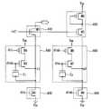
도 4는 본 발명의 일실시예에 따른 오픈 드레인 드라이버의 회로도이다. 도 4를 참조하면 본 발명의 일실시예에 따른 오픈 드레인 드라이버는 전류원(410), 전류공급부(420), 제1 풀다운 스위치부(430), 제1 풀업 스위치부(440), 제2 풀다운 스위치부(450), 및 제2 풀업 스위치부(460)를 포함한다. 전류원(410)은 도 3a 내지 도 3b에 도시된 바와 같이 엔모스 트랜지스터(M1)로 구현되며 기준전위(ref)를 입력받아 이에 해당하는 제1 기준전류를 제공한다. 제1 풀다운 스위치부(430)는 도 3a 내지 도 3d에 도시된 바와 같이 엔모스 트랜지스터(M2)로 구현되며 제1 노드(n1)와 접지전위(Vss)사이에 연결되어 입력신호(din)에 따라 스위칭을 한다.4 is a circuit diagram of an open drain driver according to an embodiment of the present invention. Referring to FIG. 4, an open drain driver according to an embodiment of the present invention may include a
도 4에 도시된 제1 풀업 스위치부(440)는 전원전압(VDD)과 제1 노드(n1) 사이에 연결되며, 제1 풀다운 스위치부(430)의 온/오프와 반대로 스위칭을 함에 있어 제1 풀다운 스위치부보다 온 되는 속도는 느리고, 오프 되는 속도는 빠른 것을 특징으로 한다. 즉, 제1 풀업 스위치부(440)는 제1 풀다운 스위치부(430)가 오프 될 때 온 되고, 제1 풀다운 스위치부(430)가 온 될 때 오프된다. 그런데 제1 풀업 스위치부(440)는 제 1 풀다운 스위치부(430)보다 온 되는 속도는 느리고 오프 되는 속도는 빠르므로 제1 풀다운 스위치부(430)가 온에서 오프로 될 때 제1 풀업 스위치부(440)는 제1 풀다운 스위치부(430)보다 느리게 오프에서 온으로 된다. 따라서 제1 풀다운 스위치부(430)가 미처 오프되지 못한 상황에서 제1 풀업 스위치부(440)가 온되는 상황이 발생하지 않아서 쇼트 전류가 발생하지 않는다. 또한, 제1 풀다운 스위치부(430)가 오프에서 온으로 될 때 제1 풀업 스위치부(440)는 제1 풀다운 스위치부(430)보드 빠르게 온에서 오프로 된다. 따라서 제1 풀업 스위치부(440)가 미처 오프되지 못한 상황에서 제1 풀다운 스위치부(430)가 온되는 상황이 발생하지 않아서 쇼트 전류가 발생하지 않는다.The first pull-up
도 4에 도시된 제1 풀업 스위치부(440)는 전원전압(VDD) 및 제1 노드(n1) 사이에 직렬로 연결된 피모스 트랜지스터(M4) 및 엔모스 트랜지스터(M3)로 구성된다. 피모스 트랜지스터(M4)의 게이트에는 입력 신호(din)가 인가되고, 엔모스 트랜지스터(M3)의 게이트에는 반전 입력 신호(dinb)가 인가된다. 따라서, 제1 풀업 스위치부(440)는 제1 풀다운 스위치부(430)와 반대로 스위칭 동작을 하게 된다. 특히, 입력 신호(din)가 '하이'에서 '로우'로 될 때 제1 풀업 스위치부(440)가 온 되어 제1 노드(n1)의 전위가 빠르게 전원전압(VDD)에서 엔모스 트랜지스터(M2)의 문턱전압(Vth)을 뺀 만큼의 전위까지 상승되도록 한다. 입력 신호(din)가 '로우'에서 '하이'로 될 때는 제1 풀업 스위치부(440)가 오프되어 전류를 흘리지 않는다. 피모스 트랜지스터(M4)는 일반적인 피모스 트랜지스터의 특성상 제1 풀다운 스위치부(430)의 엔모스 트랜지스터(M2)보다 동작속도가 느리다. 엔모스 트랜지스터(M3)는 공정시 외형비(W/L)가 엔모스 트랜지스터(M2)의 외형비보다 작은 값이 되도록 레이아웃(layout)하여 스위칭이 빠르도록 한다. 결과적으로, 제1 풀다운 스위치부(430)의 엔모스 트랜지스터(M2)보다 동작속도가 느린 피모스 트랜지스터(M4) 및 동작속도가 빠른 엔모스 트랜지스터(M3)가 직렬 연결되어 제1 풀업 스위치부(440)가 제1 풀다운 스위치부(430)보다 온 되는 속도는 느리고 오프 되는 속도는 빠르게 되는 것이다. 정리하면, 입력신호(din)가 '하이'에서 '로우'로 될 때 제1 풀업 스위치부(440)의 엔모스 트랜지스터(M3)는 빠르기 온 되나, 제1 풀업 스위치부(440)의 피모스 트랜지스터(M4)가 느리게 온 되어 결국 제1 풀업 스위치부(440)가 느리게 온 되게 된다. 다음에, 입력신호(din)가 '로우'에서 '하이'로 될 때 제1 풀업 스위치부(440)의 피모스 트랜지스터(M4)는 느리게 오프 되나, 제1 풀업 스위치부(440)의 엔모스 트랜지스터(M3)가 빠르게 오프 되어 결국 제1 풀업 스위치부(440)가 빠르게 오프 되게 된다.The first pull-
도 4에 도시된 전류공급부(420)는 도 3a 내지 도 3d에 도시된 바와 같이 다이오드 연결된 피모스 트랜지스터(M9) 및 엔모스 트랜지스터(M5)로 구현된다. 엔모스 트랜지스터(M5)는 전류원(410)을 구현하는 엔모스 트랜지스터(M1)와 대응되어 입력 신호(din) 및 반전 입력 신호(dinb)에 따른 제1 풀다운, 제1 풀업, 제2 풀다운, 및 제2 풀업 스위칭부(430, 440, 450, 460)의 스위칭 동작에도 불구하고 기준전위(ref)를 일정하게 유지하도록 한다. 제2 풀다운 스위치부(450)의 엔모스 트랜지스터(M6)는 제1 풀다운 스위치부(430)의 엔모스 트랜지스터(M2)에 대응하여 제1 풀다운 트랜지스터(M2)와 반대로 스위칭 동작을 하여 엔모스 트랜지스터(M1)와 엔모스 트랜지스터(M5)가 상호 보완적으로 동작하여 기준전위(ref)가 흔들리지 않도록 한다. 제2 풀업 스위치부(460)는 제1 풀업 스위치부(440)와 대응되도록 한 것이다. 도 4에 도시된 전류공급부(420)는 도 5에 도시된 것과 같이 드레인과 소스가 연결된 CMOS트랜지스터(M55)를 이용하여 구현하는 등 다양한 방법에 의하여 구현될 수 있음을 밝혀둔다. 이 때 CMOS트랜지스터(M55)는 엔모스 또는 피모스 트랜지스터 어느 것으로도 구현될 수 있고, CMOS트랜지스터의 게이트가 제2노드(n2)쪽으로 오고, 소스 및 드레인이 연결된 단자에 기준전위(ref)가 인가될 수도 있다.As shown in FIGS. 3A to 3D, the
도 6은 본 발명의 다른 실시예에 따른 오픈 드레인 드라이버의 회로도이다. 도 6을 참조하면 도 5에 도시된 오픈 드레인 드라이버에 비해 제1 풀업 스위치부(640)에 커패시터(C1)를 통한 반전 입력신호(dinb) 및 제1 노드(n1) 사이의 경로가 추가되어 있는 것을 알 수 있다. 또한, 제2 풀업 스위치부(660)에 커패 시터(C2)를 통한 입력신호(din) 및 제2 노드(n2) 사이의 경로가 추가되어 있다. 이와 같이 두 개의 커패시터(C1, C2)를 추가하면 입력 신호(din)가 '하이'에서 '로우'로 바뀔 때 제1 노드(n1)의 전위가 더욱 빠르게 상승함으로서 오픈 드레인 드라이버의 동작이 더욱 빨라지게 된다. 이와 같은 효과는 입력 신호(din)가 '로우'에서 '하이'로 바뀔 때 제2 노드(n2)에도 똑같이 발생한다. 도 6에서 두 개의 커패시터(C1, C2)는 소스와 드레인이 연결된 CMOS트랜지스터를 이용하여 구현하였으며, 엔모스나 피모스 트랜지스터 어느 것으로도 구현할 수 있고, 두 단자가 바뀌도록 구현할 수도 있다.6 is a circuit diagram of an open drain driver according to another exemplary embodiment of the present invention. Referring to FIG. 6, a path between the inverting input signal dinb and the first node n1 through the capacitor C1 is added to the first pull-
도 7은 종래 기술과 비교한 도 4에 도시된 오픈 드레인 드라이버의 시뮬레이션 파형도이다. 여기서 x축은 시간축이고, y축은 출력 단자에 흐르는 전류를 나타낸다. 도 7에서 파형에 S로 표시한 것은 도 3b, 도 3c에 도시된 종래기술 및 도 4에 도시된 본 발명에 따른 오픈 드레인 드라이버의 시뮬레이션 파형도이다. 도 7에서 파형에 A로 표시한 것은 도 3d에 도시된 종래기술에 따른 오픈 드레인 드라이버의 시뮬레이션 파형도이다. 도 7에서 파형에 C로 표시한 것은 도 3a에 도시된 종래기술에 따른 오픈 드레인 드라이버의 시뮬레이션 파형도이다. 도 7에서 파형에 O로 표시한 것은 도 1에 도시된 원래의 소스 스위치 방식의 오픈 드레인 드라이버의 시뮬레이션 파형도이다. 도 7을 참조하면 본 발명에 따른 오픈 드레인 드라이버가 전류 구동 타이밍상 도 3b 및 도 3d에 도시된 오픈 드레인 드라이버와 대등한 성능인 것을 알 수 있다.7 is a simulated waveform diagram of the open drain driver shown in FIG. 4 compared to the prior art. The x axis is the time axis and the y axis is the current flowing through the output terminal. In FIG. 7, the waveform S is a simulation waveform diagram of the open drain driver according to the related art shown in FIGS. 3B and 3C and the present invention shown in FIG. 4. Indicated by A on the waveform in FIG. 7 is a simulation waveform diagram of the open drain driver according to the related art shown in FIG. 3D. Indicated by C in the waveform in FIG. 7 is a simulation waveform diagram of the open drain driver according to the related art shown in FIG. 3A. 7 denoted by O in the waveform is a simulation waveform diagram of the original source switch type open-drain driver shown in FIG. 1. Referring to FIG. 7, it can be seen that the open drain driver according to the present invention has performance comparable to that of the open drain driver shown in FIGS. 3B and 3D in terms of current driving timing.
도 8은 종래기술 및 도 4에 도시된 오픈 드레인 드라이버의 출력 단자에 패 키지 모델을 접속시킨 경우의 시뮬레이션 파형도이다. 도 8에서 파형에 p로 표시한 것은 도 3b에 도시된 오픈 드레인 드라이버의 시뮬레이션 파형도이고, n으로 표시한 것은 도 3c에 도시된 오픈 드레인 드라이버의 시뮬레이션 파형도이며, s는 도 4에 도시된 본 발명에 따른 오픈 드레인 드라이버의 시뮬레이션 파형도이다. 도 8을 참조하면 오픈 드레인 드라이버의 출력단에 패키지 모델(package model)을 달아서 실제 상황에 가깝도록 한 후 시뮬레이션 하면 도 3b 및 도 3c에 도시된 오픈 드레인 드라이버보다 본 발명에 따른 오픈 드레인 드라이버가 잡음이 훨신 적은 것을 알 수 있다.8 is a simulation waveform diagram when the package model is connected to the output terminal of the prior art and the open drain driver shown in FIG. In FIG. 8, p is a simulation waveform diagram of the open drain driver shown in FIG. 3B, and n is a simulation waveform diagram of the open drain driver shown in FIG. 3C, and s is shown in FIG. 4. A simulation waveform diagram of an open drain driver according to the present invention. Referring to FIG. 8, when a package model is attached to the output terminal of the open drain driver so as to be close to the actual situation, the open drain driver according to the present invention is noisier than the open drain driver shown in FIGS. 3B and 3C. You can see much less.
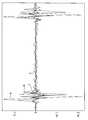
도 9는 도 8과 같은 경우에 접지전위에 흐르는 전류를 측정한 시뮬레이션 파형도이다. 도 9에서 파형에 p로 표시한 것은 도 3b에 도시된 오픈 드레인 드라이버의 시뮬레이션 파형도이고, n으로 표시한 것은 도 3c에 도시된 오픈 드레인 드라이버의 시뮬레이션 파형도이며, s는 도 4에 도시된 본 발명에 따른 오픈 드레인 드라이버의 시뮬레이션 파형도이고, o는 도 1에 도시된 원래 소스 스위치 방식의 오픈 드레인 드라이버의 파형도이다. 도 9를 참조하면 실제 패키지 모델을 출력단자에 달았을 경우에 도 3b 및 도 3c에 도시된 오픈 드레인 드라이버에 비하여 본 발명에 따른 오픈 드레인 드라이버가 기판 잡음을 현저히 줄일 수 있음을 알 수 있다.FIG. 9 is a simulation waveform diagram of measuring a current flowing in the ground potential in the case of FIG. 8. In FIG. 9, p is a simulation waveform diagram of the open drain driver shown in FIG. 3B, and n is a simulation waveform diagram of the open drain driver shown in FIG. 3C, and s is shown in FIG. 4. It is a simulation waveform diagram of the open drain driver according to the present invention, o is a waveform diagram of the original source switch type open drain driver shown in FIG. Referring to FIG. 9, when the actual package model is attached to the output terminal, it can be seen that the open drain driver according to the present invention can significantly reduce the substrate noise compared to the open drain driver illustrated in FIGS. 3B and 3C.
결국 도 7내지 도 9의 시뮬레이션 파형도를 종합하면 본 발명에 따른 오픈 드레인 드라이버가 종래기술에 비하여 상승시간, 하강시간 등의 동작속도가 빠르고, 출력전류에 잡음이 적으며, 쇼트 전류가 흐르는 전류를 방지하여 전력소모를 줄이고 기판잡음을 줄일 수 있음을 알 수 있다.7 to 9, the open drain driver according to the present invention has a faster operating speed such as a rise time and a fall time, less noise in the output current, and a short current flows as compared with the prior art. It can be seen that the power consumption can be reduced and the board noise can be reduced.
도 4 및 도 6에 도시된 오픈 드레인 드라이버에서 전류원과 제1 및 제2 풀다운 스위치부는 각각 엔모스 트랜지스터를 이용하여 구현하였으나 본 발명의 기술사상은 이러한 경우에 한하지 아니한다.In the open drain driver illustrated in FIGS. 4 and 6, the current source and the first and second pull-down switch units are implemented using NMOS transistors, respectively, but the technical concept of the present invention is not limited thereto.
설명의 편의를 위하여 본 발명의 일실시예에 따른 회로가 오픈 드레인 드라이버로 사용되는 경우를 중심으로 설명하였으나, 도 4 및 도 6에 도시된 회로는 전류 구동이 필요한 어떤 분야에서든지 적용될 수 있다. 예를 들어, 차지 펌프의 다운 스위치 및 다운 전류원을 도 4 또는 도 6에 도시된 회로를 이용하여 구현하는 경우에도 본 발명의 기술사상의 범위 내로 보아야 할 것이다.For convenience of description, the circuit according to an exemplary embodiment of the present invention is used as an open drain driver, but the circuit illustrated in FIGS. 4 and 6 may be applied to any field requiring current driving. For example, even when the down switch and the down current source of the charge pump are implemented using the circuit shown in FIG. 4 or 6, it should be considered within the scope of the technical idea of the present invention.
도 10은 본 발명의 전류 구동회로를 이용하여 구현한 차지 펌프의 회로도이다. 도 10을 참조하면 차지 펌프는 다운신호가 발생하면 출력단자로부터 다운전류를 흘려주는 다운전류 구동회로(800) 및 업신호가 발생하면 출력단자로 업전류를 흘려주는 업전류 구동회로(900)로 구성되어 있는 것을 알 수 있다. 다운전류 구동회로(800)는 도 6에 도시된 오픈 드레인 드라이버와 동일한 회로구성인 것을 알 수 있다. 다만, 기준전위대신에 제2바이어스전압(BIAS2)이 인가되고, 입력신호에 다운신호(dn)가 인가된다. 도면에 표시된 dnb는 반전된 다운신호임을 밝혀둔다. 다운전류 구동회로(800)는 다운 노드(nd)와 출력 단자 사이에 연결되어 제2바이어스전압(BIAS2)에 의해 다운전류를 공급하는 다운전류원(810), 다운 노드(nd)와 접지전위(Vss) 사이에 연결되어 다운 신호(dn)에 따라 스위칭을 하여 다운 신호가 활성화될 때만 출력단자에서 다운전류가 흐르도록 하는 다운전류 풀다운 스위치부(820), 전원전압(VDD)과 다운 노드(nd)사이에 연결되며, 다운전류 풀다 운 스위치부(820)와 반대로 스위칭을 함에 있어 다운전류 풀다운 스위치부(820)보다 온 되는 속도는 느리고 오프되는 속도는 빠른 다운전류 풀업 스위치부(830)를 포함한다. 업전류 구동회로(900)는 다운전류 구동회로와 대칭되는 구성으로 구현된다. 즉, 다운전류 구동회로(800)에서의 피모스 트랜지스터를 엔모스 트랜지스터로, 엔모스 트랜지스터를 피모스 트랜지스터로 바꾸어 놓은 구성이다. 업전류 구동회로(900)의 동작은 다운전류 구동회로(800)로부터 당해 기술분야에서 통상의 지식을 가진 자라면 용이하게 이해할 수 있는 것이다. 업전류 구동회로(900)는 업 노드(nu)와 출력 단자 사이에 연결되어 제1바이어스전압(BIAS1)에 의해 업전류를 공급하는 업전류원(910), 업 노드(nu)와 전원전압(VDD) 사이에 연결되어 반전된 업 신호(upb)에 따라 스위칭을 하여 업 신호(up)가 활성화될 때만 출력단자로 업전류가 흐르도록 하는 업전류 풀업 스위치부(920), 접지전위(Vss)와 업 노드(nu)사이에 연결되며, 업전류 풀업 스위치부(920)와 반대로 스위칭을 함에 있어 업전류 풀업 스위치부(920)보다 온 되는 속도는 느리고 오프되는 속도는 빠른 업전류 풀다운 스위치부(930)를 포함한다. 이와같이 본 발명에 따른 전류 구동회로를 차지 펌프에 적용하여 기판 잡음이 적은 차지 펌프를 구현할 수 있다.10 is a circuit diagram of a charge pump implemented using the current drive circuit of the present invention. Referring to FIG. 10, the charge pump includes a down
상기에서는 본 발명의 바람직한 실시예를 참조하여 설명하였지만, 해당 기술 분야의 숙련된 당업자는 하기의 특허 청구의 범위에 기재된 본 발명의 사상 및 영역으로부터 벗어나지 않는 범위 내에서 본 발명을 다양하게 수정 및 변경시킬 수 있음을 이해할 수 있을 것이다.Although described above with reference to a preferred embodiment of the present invention, those skilled in the art will be variously modified and changed within the scope of the invention without departing from the spirit and scope of the invention described in the claims below I can understand that you can.
상술한 바와 같이, 본 발명에 따른 오픈 드레인 드라이버 및 전류 구동방법은 풀다운 스위치부의 스위칭에 비하여 온 되는 속도는 느리고 오프 되는 속도는 빠르게 스위칭을 하는 풀업 스위치부를 구비하여 쇼트 전류가 생기는 것을 방지한다. 따라서 출력단자에 흐르는 전류에 발생하는 노이즈를 줄일 수 있고, 기판 잡음을 줄일 수 있다. 또한, 쇼트 전류의 발생을 방지하여 전력소모를 절감할 수 있다. 따라서 본 발명에 따른 오픈 드레인 드라이버를 이용하여 시스템을 구현하였을 경우에 전체 시스템이 안정적으로 동작할 수 있게 된다. As described above, the open-drain driver and the current driving method according to the present invention include a pull-up switch unit which switches on at a slower rate and a faster rate at which the off-rate is switched than the switching of the pull-down switch unit, thereby preventing short current. Therefore, the noise generated in the current flowing through the output terminal can be reduced, and the substrate noise can be reduced. In addition, power consumption can be reduced by preventing the generation of short current. Therefore, when the system is implemented using the open drain driver according to the present invention, the entire system can operate stably.
Claims (26)
Translated fromKoreanPriority Applications (5)
| Application Number | Priority Date | Filing Date | Title |
|---|---|---|---|
| KR1020040056676AKR100551474B1 (en) | 2004-07-21 | 2004-07-21 | Open Drain Driver and its Current Driving Method for Minimizing Substrate Noise |
| JP2005208860AJP4767608B2 (en) | 2004-07-21 | 2005-07-19 | Current drive circuit and charge pump using current drive circuit |
| TW094124467ATWI342671B (en) | 2004-07-21 | 2005-07-20 | Current driver circuits for reducing substrate noise and methods of operating the same |
| US11/186,115US7248077B2 (en) | 2004-07-21 | 2005-07-21 | Current driver circuits for reducing substrate noise and methods of operating the same |
| CN2005100980886ACN1728032B (en) | 2004-07-21 | 2005-07-21 | Current driver circuits for reducing substrate noise and methods of operating the same |
Applications Claiming Priority (1)
| Application Number | Priority Date | Filing Date | Title |
|---|---|---|---|
| KR1020040056676AKR100551474B1 (en) | 2004-07-21 | 2004-07-21 | Open Drain Driver and its Current Driving Method for Minimizing Substrate Noise |
Publications (2)
| Publication Number | Publication Date |
|---|---|
| KR20060009179A KR20060009179A (en) | 2006-01-31 |
| KR100551474B1true KR100551474B1 (en) | 2006-02-14 |
Family
ID=35656466
Family Applications (1)
| Application Number | Title | Priority Date | Filing Date |
|---|---|---|---|
| KR1020040056676AExpired - Fee RelatedKR100551474B1 (en) | 2004-07-21 | 2004-07-21 | Open Drain Driver and its Current Driving Method for Minimizing Substrate Noise |
Country Status (5)
| Country | Link |
|---|---|
| US (1) | US7248077B2 (en) |
| JP (1) | JP4767608B2 (en) |
| KR (1) | KR100551474B1 (en) |
| CN (1) | CN1728032B (en) |
| TW (1) | TWI342671B (en) |
Families Citing this family (6)
| Publication number | Priority date | Publication date | Assignee | Title |
|---|---|---|---|---|
| CA2669129C (en)* | 2006-11-10 | 2014-09-16 | Illuminoss Medical, Inc. | Systems and methods for internal bone fixation |
| US8415979B2 (en)* | 2010-11-04 | 2013-04-09 | Mediatek Inc. | Differential driver with calibration circuit and related calibration method |
| JP5727968B2 (en)* | 2012-05-29 | 2015-06-03 | 旭化成エレクトロニクス株式会社 | Current control circuit and PLL circuit using the same |
| CN103490618A (en)* | 2013-08-29 | 2014-01-01 | 苏州苏尔达信息科技有限公司 | Low-leakage high-speed phase-locked loop charge pump circuit |
| US9041439B2 (en)* | 2013-08-30 | 2015-05-26 | Taiwan Semiconductor Manufacturing Company, Ltd. | Transmitter having voltage driver and current driver |
| US10756720B2 (en)* | 2016-10-17 | 2020-08-25 | Infineon Technologies Ag | Driver circuit for electronic switch |
Citations (5)
| Publication number | Priority date | Publication date | Assignee | Title |
|---|---|---|---|---|
| JPH05136684A (en)* | 1991-03-07 | 1993-06-01 | Advanced Micro Devices Inc | Cmos output buffer circuit |
| JPH0629829A (en)* | 1991-06-05 | 1994-02-04 | Internatl Business Mach Corp <Ibm> | Improved bicmos exciter provided with low output level |
| KR20020087269A (en)* | 2001-05-15 | 2002-11-22 | 주식회사 하이닉스반도체 | Driver for buffering data output of semiconductor device |
| US6529050B1 (en) | 2001-08-20 | 2003-03-04 | National Semiconductor Corporation | High-speed clock buffer that has a substantially reduced crowbar current |
| JP2004120750A (en) | 2002-09-25 | 2004-04-15 | Samsung Electronics Co Ltd | I / O circuit of semiconductor device |
Family Cites Families (13)
| Publication number | Priority date | Publication date | Assignee | Title |
|---|---|---|---|---|
| JP3093410B2 (en) | 1992-01-31 | 2000-10-03 | 日本電気株式会社 | Open drain type output circuit |
| US5410189A (en)* | 1993-09-27 | 1995-04-25 | Xilinx, Inc. | Input buffer having an accelerated signal transition |
| US5497113A (en)* | 1994-05-16 | 1996-03-05 | Quantum Corporation | Variable-slope driver for pullup-terminated transmission lines |
| JPH1098380A (en)* | 1996-09-24 | 1998-04-14 | Mitsubishi Electric Corp | PLL circuit |
| US5825640A (en)* | 1997-06-30 | 1998-10-20 | Motorola, Inc. | Charge pump circuit and method |
| US6597199B1 (en)* | 1998-12-02 | 2003-07-22 | Winbond Electronics Corporation | Method and circuit for logic output buffer |
| JP3250540B2 (en)* | 1999-03-15 | 2002-01-28 | 日本電気株式会社 | PLL circuit |
| JP2001177400A (en)* | 1999-12-16 | 2001-06-29 | Sony Corp | Charge-pump circuit |
| KR100374631B1 (en)* | 2000-06-09 | 2003-03-04 | 삼성전자주식회사 | Charge pump circuit |
| KR100382718B1 (en) | 2000-08-21 | 2003-05-09 | 삼성전자주식회사 | Output driver circuit device comprising output current compensation circuit |
| US6472906B2 (en) | 2000-12-27 | 2002-10-29 | Sony Corporation | Open drain driver having enhanced immunity to I/O ground noise |
| KR100416589B1 (en)* | 2001-01-06 | 2004-02-05 | 삼성전자주식회사 | Charge pump circuit for improving switching characteristics and reducing leakage current and phase locked loop having the same |
| JP4059077B2 (en)* | 2002-12-26 | 2008-03-12 | ソニー株式会社 | Charge pump and PLL circuit using the same |
- 2004
- 2004-07-21KRKR1020040056676Apatent/KR100551474B1/ennot_activeExpired - Fee Related
- 2005
- 2005-07-19JPJP2005208860Apatent/JP4767608B2/ennot_activeExpired - Fee Related
- 2005-07-20TWTW094124467Apatent/TWI342671B/ennot_activeIP Right Cessation
- 2005-07-21USUS11/186,115patent/US7248077B2/ennot_activeExpired - Fee Related
- 2005-07-21CNCN2005100980886Apatent/CN1728032B/ennot_activeExpired - Fee Related
Patent Citations (5)
| Publication number | Priority date | Publication date | Assignee | Title |
|---|---|---|---|---|
| JPH05136684A (en)* | 1991-03-07 | 1993-06-01 | Advanced Micro Devices Inc | Cmos output buffer circuit |
| JPH0629829A (en)* | 1991-06-05 | 1994-02-04 | Internatl Business Mach Corp <Ibm> | Improved bicmos exciter provided with low output level |
| KR20020087269A (en)* | 2001-05-15 | 2002-11-22 | 주식회사 하이닉스반도체 | Driver for buffering data output of semiconductor device |
| US6529050B1 (en) | 2001-08-20 | 2003-03-04 | National Semiconductor Corporation | High-speed clock buffer that has a substantially reduced crowbar current |
| JP2004120750A (en) | 2002-09-25 | 2004-04-15 | Samsung Electronics Co Ltd | I / O circuit of semiconductor device |
Also Published As
| Publication number | Publication date |
|---|---|
| CN1728032B (en) | 2013-06-05 |
| TWI342671B (en) | 2011-05-21 |
| US20060017464A1 (en) | 2006-01-26 |
| JP2006033864A (en) | 2006-02-02 |
| TW200612663A (en) | 2006-04-16 |
| CN1728032A (en) | 2006-02-01 |
| JP4767608B2 (en) | 2011-09-07 |
| KR20060009179A (en) | 2006-01-31 |
| US7248077B2 (en) | 2007-07-24 |
Similar Documents
| Publication | Publication Date | Title |
|---|---|---|
| EP0661811B1 (en) | Level shifter circuit | |
| JP3481121B2 (en) | Level shift circuit | |
| US7843235B2 (en) | Output slew rate control in low voltage differential signal (LVDS) driver | |
| US20240372550A1 (en) | Level shifter circuit and method of operating the same | |
| KR20010049227A (en) | Level adjustment circuit and data output circuit thereof | |
| US20070024328A1 (en) | Output driver with maintained slew rate | |
| JP2007274082A (en) | Cml circuit and clock distribution circuit using same | |
| KR19990044240A (en) | Output buffer with shared intermediate node | |
| US6686779B2 (en) | Driver circuit for differentially outputting data from internal circuitry of an LSI to outside the LSI | |
| JP3354590B2 (en) | DAC current source structures, inverter structures and methods for providing these structures | |
| JP2006135560A (en) | Level shift circuit and semiconductor integrated circuit device including the same | |
| KR100551474B1 (en) | Open Drain Driver and its Current Driving Method for Minimizing Substrate Noise | |
| US20090243667A1 (en) | Output driving device | |
| JP2004153524A (en) | Level shift circuit | |
| US7133487B2 (en) | Level shifter | |
| KR102692216B1 (en) | Semiconductor device for controlling voltage of an input node of a circuit at low power mode | |
| JP2008022278A (en) | Level conversion bus switch | |
| US7183809B2 (en) | Current mode transmitter capable of canceling channel charge error | |
| KR102695245B1 (en) | Delay cell for voltage-controlled oscillator | |
| JP5689778B2 (en) | Input circuit | |
| JP2004007831A (en) | Level shift circuit | |
| US9934845B2 (en) | Latch with built-in level shifter | |
| JP3823853B2 (en) | Driving circuit and display device using the same | |
| KR100365425B1 (en) | High-Speed low static current reference circuit | |
| JP2025143979A (en) | Output control circuit and voltage output circuit |
Legal Events
| Date | Code | Title | Description |
|---|---|---|---|
| A201 | Request for examination | ||
| PA0109 | Patent application | St.27 status event code:A-0-1-A10-A12-nap-PA0109 | |
| PA0201 | Request for examination | St.27 status event code:A-1-2-D10-D11-exm-PA0201 | |
| PN2301 | Change of applicant | St.27 status event code:A-3-3-R10-R13-asn-PN2301 St.27 status event code:A-3-3-R10-R11-asn-PN2301 | |
| PN2301 | Change of applicant | St.27 status event code:A-3-3-R10-R13-asn-PN2301 St.27 status event code:A-3-3-R10-R11-asn-PN2301 | |
| D13-X000 | Search requested | St.27 status event code:A-1-2-D10-D13-srh-X000 | |
| D14-X000 | Search report completed | St.27 status event code:A-1-2-D10-D14-srh-X000 | |
| E701 | Decision to grant or registration of patent right | ||
| PE0701 | Decision of registration | St.27 status event code:A-1-2-D10-D22-exm-PE0701 | |
| PG1501 | Laying open of application | St.27 status event code:A-1-1-Q10-Q12-nap-PG1501 | |
| GRNT | Written decision to grant | ||
| PR0701 | Registration of establishment | St.27 status event code:A-2-4-F10-F11-exm-PR0701 | |
| PR1002 | Payment of registration fee | St.27 status event code:A-2-2-U10-U11-oth-PR1002 Fee payment year number:1 | |
| PG1601 | Publication of registration | St.27 status event code:A-4-4-Q10-Q13-nap-PG1601 | |
| PR1001 | Payment of annual fee | St.27 status event code:A-4-4-U10-U11-oth-PR1001 Fee payment year number:4 | |
| PR1001 | Payment of annual fee | St.27 status event code:A-4-4-U10-U11-oth-PR1001 Fee payment year number:5 | |
| PR1001 | Payment of annual fee | St.27 status event code:A-4-4-U10-U11-oth-PR1001 Fee payment year number:6 | |
| PR1001 | Payment of annual fee | St.27 status event code:A-4-4-U10-U11-oth-PR1001 Fee payment year number:7 | |
| R18-X000 | Changes to party contact information recorded | St.27 status event code:A-5-5-R10-R18-oth-X000 | |
| FPAY | Annual fee payment | Payment date:20130131 Year of fee payment:8 | |
| PR1001 | Payment of annual fee | St.27 status event code:A-4-4-U10-U11-oth-PR1001 Fee payment year number:8 | |
| FPAY | Annual fee payment | Payment date:20140129 Year of fee payment:9 | |
| PR1001 | Payment of annual fee | St.27 status event code:A-4-4-U10-U11-oth-PR1001 Fee payment year number:9 | |
| LAPS | Lapse due to unpaid annual fee | ||
| PC1903 | Unpaid annual fee | St.27 status event code:A-4-4-U10-U13-oth-PC1903 Not in force date:20150207 Payment event data comment text:Termination Category : DEFAULT_OF_REGISTRATION_FEE | |
| PC1903 | Unpaid annual fee | St.27 status event code:N-4-6-H10-H13-oth-PC1903 Ip right cessation event data comment text:Termination Category : DEFAULT_OF_REGISTRATION_FEE Not in force date:20150207 |