KR100551121B1 - Electro luminescence display - Google Patents
Electro luminescence displayDownload PDFInfo
- Publication number
- KR100551121B1 KR100551121B1KR1020030073310AKR20030073310AKR100551121B1KR 100551121 B1KR100551121 B1KR 100551121B1KR 1020030073310 AKR1020030073310 AKR 1020030073310AKR 20030073310 AKR20030073310 AKR 20030073310AKR 100551121 B1KR100551121 B1KR 100551121B1
- Authority
- KR
- South Korea
- Prior art keywords
- light emitting
- emitting layer
- transparent substrate
- packaging plate
- organic light
- Prior art date
- Legal status (The legal status is an assumption and is not a legal conclusion. Google has not performed a legal analysis and makes no representation as to the accuracy of the status listed.)
- Expired - Fee Related
Links
Images


Classifications
- H—ELECTRICITY
- H05—ELECTRIC TECHNIQUES NOT OTHERWISE PROVIDED FOR
- H05B—ELECTRIC HEATING; ELECTRIC LIGHT SOURCES NOT OTHERWISE PROVIDED FOR; CIRCUIT ARRANGEMENTS FOR ELECTRIC LIGHT SOURCES, IN GENERAL
- H05B33/00—Electroluminescent light sources
- H05B33/02—Details
- H05B33/04—Sealing arrangements, e.g. against humidity
- H—ELECTRICITY
- H10—SEMICONDUCTOR DEVICES; ELECTRIC SOLID-STATE DEVICES NOT OTHERWISE PROVIDED FOR
- H10K—ORGANIC ELECTRIC SOLID-STATE DEVICES
- H10K59/00—Integrated devices, or assemblies of multiple devices, comprising at least one organic light-emitting element covered by group H10K50/00
- H10K59/80—Constructional details
- H10K59/87—Passivation; Containers; Encapsulations
- H10K59/871—Self-supporting sealing arrangements
- H10K59/8722—Peripheral sealing arrangements, e.g. adhesives, sealants
- H—ELECTRICITY
- H10—SEMICONDUCTOR DEVICES; ELECTRIC SOLID-STATE DEVICES NOT OTHERWISE PROVIDED FOR
- H10K—ORGANIC ELECTRIC SOLID-STATE DEVICES
- H10K50/00—Organic light-emitting devices
- H10K50/80—Constructional details
- H10K50/84—Passivation; Containers; Encapsulations
- H—ELECTRICITY
- H10—SEMICONDUCTOR DEVICES; ELECTRIC SOLID-STATE DEVICES NOT OTHERWISE PROVIDED FOR
- H10K—ORGANIC ELECTRIC SOLID-STATE DEVICES
- H10K50/00—Organic light-emitting devices
- H10K50/80—Constructional details
- H10K50/84—Passivation; Containers; Encapsulations
- H10K50/842—Containers
- H10K50/8426—Peripheral sealing arrangements, e.g. adhesives, sealants
- H—ELECTRICITY
- H10—SEMICONDUCTOR DEVICES; ELECTRIC SOLID-STATE DEVICES NOT OTHERWISE PROVIDED FOR
- H10K—ORGANIC ELECTRIC SOLID-STATE DEVICES
- H10K59/00—Integrated devices, or assemblies of multiple devices, comprising at least one organic light-emitting element covered by group H10K50/00
- H10K59/80—Constructional details
- H10K59/87—Passivation; Containers; Encapsulations
- H10K59/874—Passivation; Containers; Encapsulations including getter material or desiccant
Landscapes
- Physics & Mathematics (AREA)
- Optics & Photonics (AREA)
- Electroluminescent Light Sources (AREA)
Abstract
Translated fromKoreanDescription
Translated fromKorean도 1은 일반적인 일렉트로 루미네센스 표시장치를 나타내는 단면도.1 is a cross-sectional view showing a general electro luminescence display device.
도 2는 도 1에 도시된 투명기판과 패키징 판을 합착하기 위한 합착공정을 나타내는 단면도.2 is a cross-sectional view showing a bonding process for bonding the transparent substrate and the packaging plate shown in FIG.
도 3은 도 2에 도시된 A부분을 확대하여 나타내는 단면도.3 is an enlarged cross-sectional view illustrating a portion A shown in FIG. 2.
도 4는 패키징 판에 의해 반사되는 자외선에 의한 유기 발광층의 열화로 인한 휘도차이를 나타내는 도면.4 is a diagram showing a difference in luminance due to deterioration of an organic light emitting layer by ultraviolet rays reflected by a packaging plate.
도 5는 본 발명의 제 1 실시 예에 따른 일렉트로 루미네센스 표시장치를 나타내는 단면도.5 is a cross-sectional view illustrating an electroluminescence display device according to a first embodiment of the present invention.
도 6은 도 5에 도시된 B부분을 확대하여 나타내는 단면도.6 is an enlarged cross-sectional view of a portion B shown in FIG. 5.
도 7은 본 발명의 제 2 실시 예에 따른 일렉트로 루미네센스 표시장치를 나타내는 단면도.FIG. 7 is a cross-sectional view illustrating an electro luminescence display device according to a second exemplary embodiment of the present invention. FIG.
도 8은 도 7에 도시된 C부분을 확대하여 나타내는 단면도.FIG. 8 is an enlarged cross-sectional view of a portion C shown in FIG. 7. FIG.
도 9는 본 발명의 제 3 실시 예에 따른 일렉트로 루미네센스 표시장치를 나타내는 단면도.9 is a cross-sectional view illustrating an electroluminescence display device according to a third exemplary embodiment of the present invention.
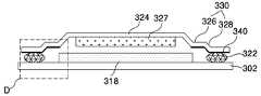
도 10은 도 9에 도시된 D부분을 확대하여 나타내는 단면도.FIG. 10 is an enlarged cross-sectional view illustrating a portion D shown in FIG. 9. FIG.
< 도면의 주요 부분에 대한 부호의 설명 ><Description of Symbols for Main Parts of Drawings>
2, 102, 202, 302 : 투명기판18, 118, 218, 318 : 유기 발광층2, 102, 202, 302:
22, 122, 222, 322 : 실링제24, 124, 224, 324 : 패키징 판22, 122, 222, 322:
26, 126, 226, 326 : 경사면27, 127, 227, 327 : 흡습막26, 126, 226, 326:
28, 128, 228, 328 : 수평면30, 130, 230, 330 : 계단형 단턱면28, 128, 228, 328:
50 : 흡착장치52 : 패드50: adsorption device 52: pad
60 : UV 조사장치62, 162, 262, 362 : 자외선60:
64 : 마스크70, 170, 270, 370 : 간접광64:
140, 240 : 광차단용 돌출부340 : 자외선 흡수층140, 240: Light blocking protrusion 340: UV absorbing layer
본 발명은 일렉트로 루미네센스 표시장치에 관한 것으로, 특히 실링 공정시 자외선에 의한 유기 발광층의 열화를 방지할 수 있는 일렉트로 루미네센스 표시장치에 관한 것이다.BACKGROUND OF THE INVENTION 1. Field of the Invention The present invention relates to an electroluminescent display device, and more particularly, to an electroluminescent display device capable of preventing deterioration of an organic light emitting layer due to ultraviolet rays during a sealing process.
음극선관(Cathode Ray Tube)의 단점인 무게와 부피를 줄일 수 있는 각종 평판 표시 장치들이 대두되고 있다. 이러한 평판 표시 장치로는 액정 표시 장치(Liquid Crystal Display), 전계 방출 표시 장치(Field Emission Display), 플라즈마 표시 패널(Plasma Display Panel) 및 일렉트로-루미네센스(Electro- Luminescence : 이하, "EL"이라 함) 표시 장치 등이 있다.Various flat panel display devices that can reduce weight and volume, which are disadvantages of cathode ray tubes, are emerging. Such flat panel displays include a liquid crystal display, a field emission display, a plasma display panel, and an electro-luminescence (hereinafter referred to as "EL"). Display device).
이들 중 EL 표시 장치는 전자와 정공의 재결합으로 형광체를 발광시키는 자발광 소자로, 그 형광체로 무기 화합물을 사용하는 무기 EL과 유기 화합물을 사용하는 유기 EL로 대별된다. 이러한 EL 표시 장치는 저전압 구동, 자기발광, 박막형, 넓은 시야각, 빠른 응답속도, 높은 콘트라스트 등의 많은 장점을 가지고 있어 차세대 표시 장치로 기대되고 있다.Among them, an EL display device is a self-luminous element that emits a phosphor by recombination of electrons and holes, and is classified roughly into an inorganic EL using an inorganic compound and an organic EL using an organic compound as the phosphor. Such EL display devices have many advantages such as low voltage driving, self-luminous, thin film type, wide viewing angle, fast response speed, and high contrast, and are expected to be the next generation display devices.
유기 EL 소자는 통상 음극과 양극 사이에 적층된 전자 주입층, 전자 수송층, 발광층, 정공 수송층, 정공 주입층으로 구성된다. 이러한 유기 EL 소자에서는 양극과 음극 사이에 소정의 전압을 인가하는 경우 음극으로부터 발생된 전자가 전자 주입층 및 전자 수송층을 통해 발광층 쪽으로 이동하고, 양극으로부터 발생된 정공이 정공 주입층 및 정공 수송층을 통해 발광층 쪽으로 이동한다. 이에 따라, 발광층에서는 전자 수송층과 정공 수송층으로부터 공급되어진 전자와 정공이 재결합함에 의해 빛을 방출하게 된다.The organic EL element is usually composed of an electron injection layer, an electron transport layer, a light emitting layer, a hole transport layer, and a hole injection layer stacked between a cathode and an anode. In such an organic EL device, when a predetermined voltage is applied between the anode and the cathode, electrons generated from the cathode move to the light emitting layer through the electron injection layer and the electron transport layer, and holes generated from the anode pass through the hole injection layer and the hole transport layer. Move toward the light emitting layer. Accordingly, the light emitting layer emits light by recombination of electrons and holes supplied from the electron transporting layer and the hole transporting layer.
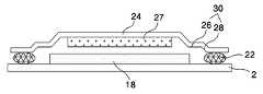
도 1을 참조하면, 종래의 EL 표시장치는 투명기판(2)과, 투명기판(2) 상에 형성된 유기 발광층(18)과, 투명기판(2) 상에 유기 발광층(18)을 밀봉하는 패키징 판(24)과, 패키징 판(24)과 투명기판(2)을 합착시키기 위한 실링제(22)를 구비한다.Referring to Fig. 1, a conventional EL display device is a package for sealing an organic
유기 발광층(18)은 도시하지 않은 음극과 양극 사이에 적층된 전자 주입층, 전자 수송층, 발광층, 정공 수송층, 정공 주입층을 구비한다. 이러한, 유기 발광층(18)은 투명전극인 양극과 금속전극인 음극 사이에 전압을 인가하면, 음극으로부 터 발생된 전자가 전자 주입층 및 전자 수송층을 통해 발광층 쪽으로 이동하고, 양극으로부터 발생된 정공이 정공 주입층 및 정공 수송층을 통해 발광층 쪽으로 이동한다. 이에 따라, 발광층에서는 전자 수송층과 정공 수송층으로부터 공급되어진 전자와 정공이 충돌하여 재결합함에 의해 빛이 발생하게 되고, 이 빛은 투명전극인 양극을 통해 외부로 방출되어 화상이 표시되게 한다.The organic
패키징 판(24)은 대기 중의 수분 및 산소를 흡수하여 대기 중의 수분 및 산소로부터 유기 발광층(18)을 보호하기 위한 흡습막(27)이 부착된다. 이를 위해, 패키징 판(24)은 경사면(26)과 수평면(28)을 가지는 계단형 단턱부(30)를 구비한다. 이 계단형 단턱부(30)에 의해 패키징 판(24)의 중앙부에는 흡습막(27)이 부착되는 내부공간이 마련된다.The
실링제(22)는 패키징 판(24)의 최외곽 단턱면(28)과 투명기판(2) 사이에 도포된 후, 조사되는 자외선에 의해 경화됨으로써 패키징 판(24)과 투명기판(2)을 합착시키게 된다. 이로 인하여, 패키징 판(24)은 진공 상태에서 실링제(22)에 의해 투명기판(2)과 합착되어 유기 발광층(18)을 밀봉하게 된다.The
이러한, 종래의 일렉트로 루미네센스 표시장치는 도 2에 도시된 바와 같은 합착장치에 의해 투명기판(2)과 패키징 판(24)을 합착시키게 된다.In such a conventional electroluminescent display device, the
구체적으로, 합착장치는 다수의 유기 발광층(18)이 형성되고 도시하지 않은 고정수단에 의해 고정된 대형 투명기판(2)과, 다수의 유기 발광층(18)과 합착되는 다수의 패키징 판(24)이 흡착된 다수의 흡착장치(50)와, 투명기판(2) 또는 패키징 판(24)의 가장자리에 도포된 실링제(24)와, 실링제(24)에 자외선(62)을 조사하기 위한 UV 조사장치(60)와, 유기 발광층(18) 각각에 자외선(62)이 조사되지 않도록 실링제(24)를 제외한 다른 영역을 마스킹하는 마스크(64)를 구비한다.Specifically, the bonding apparatus includes a large
흡착장치(50)는 패드(52)를 이용하여 외부로부터 공급되는 패키징 판(24)을 흡착하게 된다.The
이러한, 합착장치는 흡착장치(50)의 패드(52) 상에 패키징 판(24)이 흡착되고, 고정수단에 의해 투명기판(2)이 고정되며 패키징 판(24)과 투명기판(2) 상에 형성된 유기 발광층(18)을 얼라인시키게 된다.Such a bonding apparatus has a
그런 다음, UV 조사장치(60)로부터 자외선을 투명기판(2)과 패키징 판(24) 사이에 도포된 실링제(22)에 자외선(62)을 소정시간 동안 조사하게 된다. 이 때, 마스크(64)는 UV 조사장치(60)로부터 조사되는 자외선(62)이 투명기판(2)과 패키징 판(24) 사이에 도포된 실링제(22)에만 조사되고 나머지는 차단시키게 된다.Then, the ultraviolet ray is irradiated from the
이에 따라, 실링제(22)는 마스크(64)를 경유하여 조사되는 자외선(62)에 의해 경화되어 투명기판(2)과 패키징 판(24)을 합착시키게 된다.Accordingly, the
이와 같이, 실링제(22)에 자외선(64)을 조사하여 투명기판(2)과 패키징 판(24)을 합착시킬 경우에 마스크(64)를 경유하여 실링제(22)에 조사되는 자외선(64)은 도 3에 도시된 바와 같이 패키징 판(24)에 형성된 계단형 단턱부(30)의 경사면(26)에 의해 자외선(64)의 산란에 의한 간접광(70)이 발생하게 된다. 즉, 자외선(64)은 실링제(22)에 조사되어 실링제(22)를 경화시킴과 아울러 패키징 판(24)에 형성된 계단형 단턱부(30)의 경사면(26)에 의해 산란되어 간접광(70)을 발생하게 된다. 이러한, 간접광(70)은 패키징 판(24)에 형성된 계단형 단턱부(30) 의 경사면(26) 및 단턱면(28)과 투명기판(2) 사이에서 반사 및 재반사를 반복하여 유기 발광층(18) 및 EL 표시소자의 주변부에 조사된다. 이에 따라, 간접광(70)은 유기 발광층(18)에 조사되어 유기 발광층(18)을 열화시킴과 아울러 EL 표시소자의 주변부에 조사되어 EL 표시소자의 주변회로의 트랜지스터를 포함하는 구동소자들의 특성을 변화시키게 된다.As described above, when the
따라서, 종래의 EL 표시장치는 투명기판(2)과 패키징 판(24)의 합착공정시 실링제(22)에 조사된 자외선(64)의 산란에 의한 간접광(70)에 의해 유기 발광층(18)의 가장자리가 열화됨과 아울러 주변회로의 구동소자들의 특성이 변함으로써 도 4에 도시된 바와 같이 EL 표시장치의 중앙부(80)와 그 외의 영역(82) 간의 휘도 차이가 발생하게 된다.Therefore, in the conventional EL display device, the organic
따라서, 본 발명의 목적은 실링 공정시 자외선에 의한 유기 발광층의 열화를 방지할 수 있는 일렉트로 루미네센스 표시장치를 제공하는데 있다.
Accordingly, an object of the present invention is to provide an electro luminescence display device that can prevent degradation of the organic light emitting layer due to ultraviolet rays during the sealing process.
상기 목적을 달성하기 위하여, 본 발명의 실시 예에 따른 일렉트로 루미네센스 표시장치는 투명기판과, 상기 투명기판 상에 형성되는 유기 발광층과, 실링제의 의해 상기 투명기판과 합착되어 상기 유기 발광층을 감싸는 패키징 판과, 상기 투명기판과 상기 패키징 판의 합착시 상기 실링제에 조사되는 자외선이 상기 패키징 판에 의해 반사되어 상기 유기 발광층에 조사되는 것을 차단하는 광차단 부재를 구비하는 것을 특징으로 한다.In order to achieve the above object, an electro luminescence display device according to an embodiment of the present invention is bonded to the transparent substrate by a transparent substrate, an organic light emitting layer formed on the transparent substrate, and a sealing agent to form the organic light emitting layer. And a light blocking member that surrounds the packaging plate and the ultraviolet ray irradiated to the sealing agent when the transparent substrate and the packaging plate are bonded to each other, thereby preventing the organic light emitting layer from being reflected by the packaging plate.
상기 일렉트로 루미네센스 표시장치에서 상기 광차단 부재는 상기 패키징 판으로부터 상기 투명기판 쪽으로 돌출되는 광차단용 돌출부인 것을 특징으로 한다.In the electro luminescence display, the light blocking member is a light blocking protrusion protruding from the packaging plate toward the transparent substrate.
상기 일렉트로 루미네센스 표시장치에서 상기 광차단용 돌출부는 상기 실링제와 상기 유기 발광층 사이에 위치하는 것을 특징으로 한다.In the electro luminescence display, the light blocking protrusion may be positioned between the sealing agent and the organic light emitting layer.
상기 일렉트로 루미네센스 표시장치에서 상기 광차단용 돌출부는 상기 유기 발광층에 최대한 근접되도록 상기 패키징 판에서 돌출되는 것을 특징으로 한다.The light blocking protrusion of the electroluminescent display device may protrude from the packaging plate to be as close as possible to the organic light emitting layer.
상기 일렉트로 루미네센스 표시장치에서 상기 광차단용 돌출부는 사각형 및 삼각형 중 어느 한 형태의 단면을 가지도록 형성되는 것을 특징으로 한다.In the electro luminescence display, the light blocking protrusion may be formed to have a cross section of any one of a rectangle and a triangle.
상기 일렉트로 루미네센스 표시장치에서 상기 광차단 부재는 상기 투명기판에서 상기 패키징 판 쪽으로 돌출되는 다수의 광차단용 돌출부인 것을 특징으로 한다.In the electro luminescence display, the light blocking member is a plurality of light blocking protrusions protruding from the transparent substrate toward the packaging plate.
상기 일렉트로 루미네센스 표시장치에서 상기 다수의 광차단용 돌출부는 상기 투명기판의 끝단과 상기 유기 발광층 사이에 형성되는 것을 특징으로 한다.In the electro luminescence display, the plurality of light blocking protrusions may be formed between an end of the transparent substrate and the organic light emitting layer.
상기 일렉트로 루미네센스 표시장치에서 상기 다수의 광차단용 돌출부 각각은 사각형 및 삼각형 중 어느 한 형태의 단면을 가지도록 형성되는 것을 특징으로 한다.In the electro luminescence display, each of the plurality of light blocking protrusions may be formed to have a cross section of any one of a rectangle and a triangle.
상기 일렉트로 루미네센스 표시장치에서 상기 광차단 부재는 상기 투명기판과 대향하도록 상기 패키징 판에 형성되어 상기 자외선을 흡수하는 자외선 흡수층 인 것을 특징으로 한다.In the electro luminescence display, the light blocking member is an ultraviolet absorbing layer formed on the packaging plate to face the transparent substrate and absorbing the ultraviolet rays.
상기 일렉트로 루미네센스 표시장치에서 상기 자외선 흡수층은 상기 유기 발광층의 가장자리와 상기 투명기판의 끝단 사이와 대향함과 아울러 상기 유기 발광층의 가장자리와 중첩되는 되도록 상기 패키징 판의 가장자리에 형성되는 것을 특징으로 한다.In the electro luminescence display, the ultraviolet light absorbing layer is formed on the edge of the packaging plate so as to face between the edge of the organic light emitting layer and the end of the transparent substrate and overlap the edge of the organic light emitting layer. .
상기 목적 외에 본 발명의 다른 목적 및 특징들은 첨부도면을 참조한 실시 예에 대한 설명을 통하여 명백하게 드러나게 될 것이다.Other objects and features of the present invention in addition to the above object will be apparent from the description of the embodiments with reference to the accompanying drawings.
이하, 도 5 내지 도 10을 참조하여 본 발명의 바람직한 실시 예에 대하여 설명하기로 한다.Hereinafter, exemplary embodiments of the present invention will be described with reference to FIGS. 5 to 10.
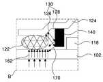
도 5를 참조하면, 본 발명의 제 1 실시 예에 따른 일렉트로 루미네센스 표시장치는 투명기판(102)과, 투명기판(102) 상에 형성된 유기 발광층(118)과, 투명기판(102) 상에 유기 발광층(118)을 밀봉하는 패키징 판(124)과, 패키징 판(124)과 투명기판(102)을 합착시키기 위한 실링제(122)와, 패키징 판(124)에 형성되어 패키징 판(124)과 투명기판(102) 합착시 실링제(122)에 조사되는 자외선이 유기 발광층(118)으로 조사되는 것을 방지하는 적어도 하나의 광차단용 돌출부(140)를 구비한다.Referring to FIG. 5, an electroluminescent display device according to a first exemplary embodiment of the present invention includes a
유기 발광층(118)은 도시하지 않은 음극과 양극 사이에 적층된 전자 주입층, 전자 수송층, 발광층, 정공 수송층, 정공 주입층을 구비한다. 이러한, 유기 발광층(118)은 투명전극인 양극과 금속전극인 음극 사이에 전압을 인가하면, 음극으로부터 발생된 전자가 전자 주입층 및 전자 수송층을 통해 발광층 쪽으로 이동하고, 양극으로부터 발생된 정공이 정공 주입층 및 정공 수송층을 통해 발광층 쪽으로 이동한다. 이에 따라, 발광층에서는 전자 수송층과 정공 수송층으로부터 공급되어진 전자와 정공이 충돌하여 재결합함에 의해 빛이 발생하게 되고, 이 빛은 투명전극인 양극을 통해 외부로 방출되어 화상이 표시되게 한다.The organic
패키징 판(124)은 실링제(122)에 의해 투명기판(102)과 합착되어 유기 발광층(118)을 감싸게 된다. 이러한, 패키징 판(124)은 대기 중의 수분 및 산소를 흡수하여 대기 중의 수분 및 산소로부터 유기 발광층(118)을 보호하기 위한 흡습막(127)이 부착된다. 이를 위해, 패키징 판(124)은 경사면(126)과 수평면(128)을 가지는 계단형 단턱부(130)를 구비한다. 이 계단형 단턱부(130)에 의해 패키징 판(124)의 중앙부에는 흡습막(127)이 부착되는 내부공간이 마련된다.The
실링제(122)는 패키징 판(124)의 최외곽 단턱면(128)과 투명기판(102) 사이에 도포된 후, 외부로부터 조사되는 자외선에 의해 경화됨으로써 패키징 판(124)과 투명기판(102)을 합착시키게 된다. 이로 인하여, 패키징 판(124)은 진공 상태에서 실링제(122)에 의해 투명기판(102)과 합착되어 유기 발광층(118)을 밀봉하게 된다.The sealing
적어도 하나의 광차단용 돌출부(140)는 실링제(122)와 유기 발광층(118) 사이에 대응되는 패키징 판(124) 상에서 사각형 및 삼각형 중 어느 한 형태의 단면을 가지도록 투명기판(102) 쪽으로 돌출된다. 이 때, 광차단용 돌출부(140)는 유기 발광층(118)에 최대한 근접됨과 아울러 투명기판(102)과 소정 갭을 가지도록 근접되도록 돌출된다. 이러한, 광차단용 돌출부(140)는 패키징 판(124)의 경사면(126)에 의해 투명기판(102)과 패키징 판(124)의 합착 공정시 실링제(122)에 조사되는 자외선이 산란되어 유기 발광층(118)의 열화 및 EL 표시소자의 주변부의 구동소자들에 조사되는 것을 차단하게 된다.The at least one
구체적으로, 본 발명의 제 1 실시 예에 따른 일렉트로 루미네센스 표시장치는 우선 유기 발광층(118)이 형성된 투명기판(102)과 유기 발광층(118)을 대기 중의 산소 및 수분으로부터 보호하는 패키징 판(124) 중 어느 하나의 가장자리에 도포된 실링제(122)에 자외선을 조사하여 실링제(122)를 경화시킴으로써 투명기판(102)과 패키징 판(124)을 합착시키게 된다. 이 때, 광차단용 돌출부(140)는 도 6에 도시된 바와 같이 실링제(122)에 조사되는 자외선(162)이 패키징 판(124)의 경사면(126)에 의해 산란되어 발생되는 간접광(170)이 유기 발광층(118) 및 EL 표시소자의 주변부의 구동소자들에 조사되는 것을 실링제(122) 쪽으로 반사시켜 차단하게 된다. 따라서, 본 발명의 제 1 실시 예에 따른 일렉트로 루미네센스 표시장치는 실링제(122)의 경화시 패키징 판(124)에 의해 발생되는 간접광(170)으로 인한 유기 발광층(118)의 열화 및 EL 표시소자의 주변부의 구동소자들의 특성변화를 방지하게 된다.Specifically, the electroluminescent display device according to the first exemplary embodiment of the present invention is a packaging plate for protecting the
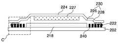
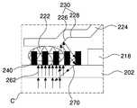
도 7을 참조하면, 본 발명의 제 2 실시 예에 따른 일렉트로 루미네센스 표시장치는 투명기판(202)과, 투명기판(202) 상에 형성된 유기 발광층(218)과, 투명기판(202) 상에 유기 발광층(218)을 밀봉하는 패키징 판(224)과, 패키징 판(224)과 투명기판(202)을 합착시키기 위한 실링제(222)와, 투명기판(202)으로부터 패키징 판(224) 쪽으로 돌출되어 패키징 판(224)과 투명기판(202) 합착시 실링제(222)에 조사되는 자외선의 산란에 의한 간접광이 유기 발광층(218)으로 조사되는 것을 방 지하기 위한 다수의 광차단용 돌출부(240)를 구비한다.Referring to FIG. 7, an electro luminescence display device according to a second exemplary embodiment of the present invention includes a
유기 발광층(218)은 도시하지 않은 음극과 양극 사이에 적층된 전자 주입층, 전자 수송층, 발광층, 정공 수송층, 정공 주입층을 구비한다. 이러한, 유기 발광층(218)은 투명전극인 양극과 금속전극인 음극 사이에 전압을 인가하면, 음극으로부터 발생된 전자가 전자 주입층 및 전자 수송층을 통해 발광층 쪽으로 이동하고, 양극으로부터 발생된 정공이 정공 주입층 및 정공 수송층을 통해 발광층 쪽으로 이동한다. 이에 따라, 발광층에서는 전자 수송층과 정공 수송층으로부터 공급되어진 전자와 정공이 충돌하여 재결합함에 의해 빛이 발생하게 되고, 이 빛은 투명전극인 양극을 통해 외부로 방출되어 화상이 표시되게 한다.The organic
패키징 판(224)은 실링제(222)에 의해 투명기판(202)과 합착되어 유기 발광층(218)을 감싸게 된다. 이러한, 패키징 판(224)은 대기 중의 수분 및 산소를 흡수하여 대기 중의 수분 및 산소로부터 유기 발광층(218)을 보호하기 위한 흡습막(227)이 부착된다. 이를 위해, 패키징 판(224)은 경사면(226)과 수평면(228)을 가지는 계단형 단턱부(230)를 구비한다. 이 계단형 단턱부(230)에 의해 패키징 판(224)의 중앙부에는 흡습막(227)이 부착되는 내부공간이 마련된다.The
실링제(222)는 패키징 판(224)의 최외곽 단턱면(228)과 투명기판(202) 사이에 도포된 후, 외부로부터 조사되는 자외선에 의해 경화됨으로써 패키징 판(224)과 투명기판(202)을 합착시키게 된다. 이로 인하여, 패키징 판(224)은 진공 상태에서 실링제(222)에 의해 투명기판(202)과 합착되어 유기 발광층(218)을 밀봉하게 된다.The sealing
다수의 광차단용 돌출부(240)는 투명기판(202)의 가장자리 상에서 사각형 및 삼각형 중 어느 한 형태의 단면을 가지도록 투명기판(102) 쪽으로 돌출된다. 즉, 다수의 광차단용 돌출부(240)는 투명기판(202)의 끝단과 유기 발광층(218) 사이에 형성되고, 다수의 광차단용 돌출부(240)의 일부 상에는 실링제(222)가 도포된다. 이러한, 다수의 광차단용 돌출부(240)는 패키징 판(224)의 경사면(226)에 의해 투명기판(202)과 패키징 판(224)의 합착 공정시 실링제(222)에 조사되는 자외선이 산란되어 유기 발광층(218)의 열화 및 EL 표시소자의 주변부의 구동소자들에 조사되는 것을 차단하게 된다.The plurality of light blocking
구체적으로, 본 발명의 제 2 실시 예에 따른 일렉트로 루미네센스 표시장치는 우선 유기 발광층(218)이 형성된 투명기판(202)과 유기 발광층(218)을 대기 중의 산소 및 수분으로부터 보호하는 패키징 판(224) 중 어느 하나의 가장자리에 도포된 실링제(222)에 자외선을 조사하여 실링제(222)를 경화시킴으로써 투명기판(202)과 패키징 판(224)을 합착시키게 된다. 이 때, 다수의 광차단용 돌출부(240)는 도 8에 도시된 바와 같이 실링제(222)에 조사되는 자외선(262)이 패키징 판(224)의 경사면(226)에 의해 산란되어 발생되는 간접광(270)이 유기 발광층(218) 및 EL 표시소자의 주변부의 구동소자들에 조사되는 것을 실링제(222) 쪽으로 반사시켜 차단하게 된다. 이를 위해, 다수의 광차단용 돌출부(240)는 간접광(270)이 패키징 판(224)에 의해 유기 발광층(218)으로 진행하는 것을 차단하기 위하여 최대한 패키징 판(224)에 근접되도록 투명기판(202) 상에 돌출된다.Specifically, the electroluminescent display device according to the second exemplary embodiment of the present invention is a packaging plate for protecting the
따라서, 본 발명의 제 2 실시 예에 따른 일렉트로 루미네센스 표시장치는 실링제(222)의 경화시 패키징 판(224)에 의해 발생되는 간접광(270)으로 인한 유기 발광층(218)의 열화 및 EL 표시소자의 주변부의 구동소자들의 특성변화를 방지하게 된다. Accordingly, the electroluminescent display device according to the second embodiment of the present invention may deteriorate the organic
도 9를 참조하면, 본 발명의 제 3 실시 예에 따른 일렉트로 루미네센스 표시장치는 투명기판(302)과, 투명기판(302) 상에 형성된 유기 발광층(318)과, 투명기판(302) 상에 유기 발광층(318)을 밀봉하는 패키징 판(324)과, 패키징 판(324)과 투명기판(302)을 합착시키기 위한 실링제(322)와, 패키징 판(324)에 형성되어 패키징 판(324)과 투명기판(302) 합착시 실링제(322)에 조사되는 자외선이 유기 발광층(318)으로 조사되는 것을 방지하는 자외선 흡수층(340)을 구비한다.Referring to FIG. 9, an electroluminescent display device according to a third exemplary embodiment of the present invention includes a
유기 발광층(318)은 도시하지 않은 음극과 양극 사이에 적층된 전자 주입층, 전자 수송층, 발광층, 정공 수송층, 정공 주입층을 구비한다. 이러한, 유기 발광층(318)은 투명전극인 양극과 금속전극인 음극 사이에 전압을 인가하면, 음극으로부터 발생된 전자가 전자 주입층 및 전자 수송층을 통해 발광층 쪽으로 이동하고, 양극으로부터 발생된 정공이 정공 주입층 및 정공 수송층을 통해 발광층 쪽으로 이동한다. 이에 따라, 발광층에서는 전자 수송층과 정공 수송층으로부터 공급되어진 전자와 정공이 충돌하여 재결합함에 의해 빛이 발생하게 되고, 이 빛은 투명전극인 양극을 통해 외부로 방출되어 화상이 표시되게 한다.The organic
패키징 판(324)은 실링제(322)에 의해 투명기판(302)과 합착되어 유기 발광층(318)을 감싸게 된다. 이러한, 패키징 판(324)은 대기 중의 수분 및 산소를 흡수하여 대기 중의 수분 및 산소로부터 유기 발광층(318)을 보호하기 위한 흡습막(327)이 부착된다. 이를 위해, 패키징 판(324)은 경사면(326)과 수평면(328)을 가지는 계단형 단턱부(330)를 구비한다. 이 계단형 단턱부(330)에 의해 패키징 판(324)의 중앙부에는 흡습막(327)이 부착되는 내부공간이 마련된다.The
실링제(322)는 패키징 판(324)의 최외곽 단턱면(328)과 투명기판(302) 사이에 도포된 후, 외부로부터 조사되는 자외선에 의해 경화됨으로써 패키징 판(324)과 투명기판(302)을 합착시키게 된다. 이로 인하여, 패키징 판(324)은 진공 상태에서 실링제(322)에 의해 투명기판(302)과 합착되어 유기 발광층(318)을 밀봉하게 된다.The sealing
자외선 흡수층(340)은 투명기판(202)의 가장자리에 대응되는 패키징 판(324)의 가장자리의 수평면(328) 및 경사면(326)에 형성된다. 즉, 자외선 흡수층(340)은 투명기판(302)의 끝단과 유기 발광층(318)의 끝단 사이에 대향되도록 패키징 판(324)의 배면에 형성된다. 이 때, 자외선 흡수층(340)은 유기 발광층(318)의 가장자리 영역과 중첩되도록 형성된다. 이러한, 자외선 흡수층(340)은 패키징 판(324)의 경사면(326)에 의해 투명기판(302)과 패키징 판(324)의 합착 공정시 실링제(322)에 조사되는 자외선이 산란되어 유기 발광층(318)의 열화 및 EL 표시소자의 주변부의 구동소자들에 조사되는 것을 차단하게 된다.The
구체적으로, 본 발명의 제 3 실시 예에 따른 일렉트로 루미네센스 표시장치는 우선 유기 발광층(318)이 형성된 투명기판(302)과 유기 발광층(318)을 대기 중의 산소 및 수분으로부터 보호하는 패키징 판(324) 중 어느 하나의 가장자리에 도포된 실링제(322)에 자외선을 조사하여 실링제(322)를 경화시킴으로써 투명기판(302)과 패키징 판(324)을 합착시키게 된다. 이 때, 자외선 흡수층(340)은 도 10에 도시된 바와 같이 실링제(322)에 조사되는 자외선(362)이 패키징 판(324)의 경사면(326) 및 수평면(328)에 의해 유기 발광층(318) 쪽으로 반사되는 자외선(362)을 흡수하게 된다. 즉, 자외선 흡수층(340)은 조사되는 자외선(362)의 반사효율을 감소시켜 패키징 판(324)의 경사면(326) 및 수평면(328)에 의해 산란되어 발생되는 간접광(370)이 유기 발광층(318) 쪽으로 반사되는 것을 차단하게 된다. 따라서, 본 발명의 제 3 실시 예에 따른 일렉트로 루미네센스 표시장치는 실링제(322)의 경화시 패키징 판(324)에 의해 발생되는 간접광(370)으로 인한 유기 발광층(318)의 열화 및 EL 표시소자의 주변부의 구동소자들의 특성변화를 방지하게 된다.Specifically, the electroluminescent display device according to the third exemplary embodiment of the present invention is a packaging plate for protecting the organic
상술한 바와 같이, 본 발명의 실시 예에 따른 일렉트로 루미네센스 표시장치는 패키징 판의 가장자리에서 투명기판 쪽으로 돌출되는 광차단용 돌출부를 구비한다. 이에 따라, 본 발명은 광차단용 돌출부를 이용하여 투명기판과 패키징 판의 합착시 실링제에 조사되는 자외선이 패키징 판에 의해 반사되어 유기 발광층으로 조사되는 자외선을 차단함으로써 유기 발광층의 열화 및 EL 표시소자의 주변부의 구동소자들의 특성변화를 방지하게 된다.As described above, the electro luminescence display device according to the embodiment of the present invention includes a light blocking protrusion protruding from the edge of the packaging plate toward the transparent substrate. Accordingly, the present invention is to deteriorate the organic light emitting layer and EL display by blocking the ultraviolet light is irradiated to the organic light emitting layer is reflected by the packaging plate when the transparent substrate and the packaging plate is bonded by using the light blocking protrusion portion It is possible to prevent the characteristic change of the driving elements in the peripheral portion of the device.
또한, 본 발명의 다른 실시 예에 다른 일렉트로 루미네센스 표시장치는 투명기판의 가장자리에서 패키징 판 쪽으로 돌출되는 다수의 광차단용 돌출부를 구비한다. 이에 따라, 본 발명은 다수의 광차단용 돌출부를 이용하여 투명기판과 패키징 판의 합착시 실링제에 조사되는 자외선이 패키징 판에 의해 반사되어 유기 발광층 으로 조사되는 자외선을 차단함으로써 유기 발광층의 열화 및 EL 표시소자의 주변부의 구동소자들의 특성변화를 방지하게 된다.In addition, an electroluminescent display device according to another embodiment of the present invention includes a plurality of light blocking protrusions protruding from the edge of the transparent substrate toward the packaging plate. Accordingly, the present invention deteriorates the organic light emitting layer by blocking ultraviolet rays irradiated to the organic light emitting layer by reflecting the ultraviolet rays irradiated to the sealing plate when the transparent substrate and the packaging plate are bonded by using a plurality of light blocking protrusions. The characteristic change of the driving elements in the periphery of the EL display element is prevented.
또한, 본 발명의 또 다른 실시 예에 따른 일렉트로 루미네센스 표시장치는 패키징 판의 가장자리에 형성되는 자외선 흡수층을 구비한다. 이에 따라, 본 발명은 자외선 흡수층을 이용하여 투명기판과 패키징 판의 합착시 실링제에 조사되는 자외선이 패키징 판에 의해 반사되어 유기 발광층으로 조사되는 자외선을 흡수함으로써 유기 발광층의 열화 및 EL 표시소자의 주변부의 구동소자들의 특성변화를 방지하게 된다.In addition, the electro luminescence display according to another embodiment of the present invention includes an ultraviolet absorbing layer formed on the edge of the packaging plate. Accordingly, the present invention absorbs ultraviolet rays irradiated to the organic light emitting layer by reflecting the ultraviolet rays irradiated to the sealing plate when the transparent substrate and the packaging plate are bonded by the ultraviolet absorbing layer to deteriorate the organic light emitting layer and the EL display device. It is possible to prevent the characteristic change of the driving elements in the peripheral portion.
이상 설명한 내용을 통해 당업자라면 본 발명의 기술사상을 일탈하지 아니하는 범위에서 다양한 변경 및 수정이 가능함을 알 수 있을 것이다. 따라서, 본 발명의 기술적 범위는 명세서의 상세한 설명에 기재된 내용으로 한정되는 것이 아니라 특허 청구의 범위에 의해 정하여 져야만 할 것이다.Those skilled in the art will appreciate that various changes and modifications can be made without departing from the technical spirit of the present invention. Therefore, the technical scope of the present invention should not be limited to the contents described in the detailed description of the specification but should be defined by the claims.
Claims (10)
Translated fromKoreanPriority Applications (3)
| Application Number | Priority Date | Filing Date | Title |
|---|---|---|---|
| KR1020030073310AKR100551121B1 (en) | 2003-10-21 | 2003-10-21 | Electro luminescence display |
| US10/968,186US7189990B2 (en) | 2003-10-21 | 2004-10-20 | Electro luminescence display device |
| EP04024957AEP1526589A3 (en) | 2003-10-21 | 2004-10-20 | Electro luminescence display device |
Applications Claiming Priority (1)
| Application Number | Priority Date | Filing Date | Title |
|---|---|---|---|
| KR1020030073310AKR100551121B1 (en) | 2003-10-21 | 2003-10-21 | Electro luminescence display |
Publications (2)
| Publication Number | Publication Date |
|---|---|
| KR20050038101A KR20050038101A (en) | 2005-04-27 |
| KR100551121B1true KR100551121B1 (en) | 2006-02-13 |
Family
ID=34386784
Family Applications (1)
| Application Number | Title | Priority Date | Filing Date |
|---|---|---|---|
| KR1020030073310AExpired - Fee RelatedKR100551121B1 (en) | 2003-10-21 | 2003-10-21 | Electro luminescence display |
Country Status (3)
| Country | Link |
|---|---|
| US (1) | US7189990B2 (en) |
| EP (1) | EP1526589A3 (en) |
| KR (1) | KR100551121B1 (en) |
Cited By (1)
| Publication number | Priority date | Publication date | Assignee | Title |
|---|---|---|---|---|
| KR20160107395A (en)* | 2015-03-03 | 2016-09-19 | 삼성디스플레이 주식회사 | Display device |
Families Citing this family (11)
| Publication number | Priority date | Publication date | Assignee | Title |
|---|---|---|---|---|
| US8405193B2 (en)* | 2004-04-02 | 2013-03-26 | General Electric Company | Organic electronic packages having hermetically sealed edges and methods of manufacturing such packages |
| KR100892413B1 (en)* | 2007-10-12 | 2009-04-10 | 전자부품연구원 | Organic light emitting diode lighting device and manufacturing method thereof |
| KR101023129B1 (en)* | 2008-07-25 | 2011-03-18 | 삼성모바일디스플레이주식회사 | Organic light emitting display and manufacturing method thereof |
| KR101146985B1 (en) | 2010-03-11 | 2012-05-23 | 삼성모바일디스플레이주식회사 | Display device and method of manufacturing the same |
| TWI574442B (en)* | 2014-04-10 | 2017-03-11 | 友達光電股份有限公司 | Display panel |
| CN105470410B (en)* | 2016-02-24 | 2018-05-29 | 上海天马有机发光显示技术有限公司 | A kind of display panel and its method for packing |
| CN106935731B (en)* | 2017-05-15 | 2020-03-06 | 京东方科技集团股份有限公司 | Organic electroluminescent display device and display device |
| KR102430794B1 (en)* | 2017-11-30 | 2022-08-08 | 엘지디스플레이 주식회사 | Display apparatus |
| CN109950414A (en)* | 2019-01-31 | 2019-06-28 | 昆山国显光电有限公司 | A kind of display panel and display equipment |
| CN110571347B (en)* | 2019-08-09 | 2021-04-02 | 武汉华星光电半导体显示技术有限公司 | Display panel and preparation method thereof |
| CN114709348A (en)* | 2022-03-31 | 2022-07-05 | 武汉天马微电子有限公司 | Display modules and display devices |
Family Cites Families (14)
| Publication number | Priority date | Publication date | Assignee | Title |
|---|---|---|---|---|
| US3997892A (en)* | 1973-07-27 | 1976-12-14 | Trw Inc. | Digital to analog converter with improved companding |
| US5482896A (en)* | 1993-11-18 | 1996-01-09 | Eastman Kodak Company | Light emitting device comprising an organic LED array on an ultra thin substrate and process for forming same |
| DE69739955D1 (en) | 1996-02-26 | 2010-09-16 | Idemitsu Kosan Co | Organic electroluminescent device and process for its preparation |
| EP0899987A1 (en)* | 1997-08-29 | 1999-03-03 | TDK Corporation | Organic electroluminescent device |
| JP2000150145A (en) | 1998-11-02 | 2000-05-30 | Toyota Motor Corp | EL element sealing method |
| US6383664B2 (en)* | 1999-05-11 | 2002-05-07 | The Dow Chemical Company | Electroluminescent or photocell device having protective packaging |
| US6225931B1 (en)* | 1999-08-30 | 2001-05-01 | Industrial Technology Research Institute | D/A converter with a gamma correction circuit |
| JP2001126868A (en) | 1999-10-28 | 2001-05-11 | Idemitsu Kosan Co Ltd | Method for manufacturing organic electroluminescence device |
| WO2001045140A2 (en)* | 1999-12-17 | 2001-06-21 | Osram Opto Semiconductors Gmbh | Encapsulation for organic led device |
| JP2002156938A (en)* | 2000-11-21 | 2002-05-31 | Canon Inc | Image display device and its driving method |
| US6537688B2 (en)* | 2000-12-01 | 2003-03-25 | Universal Display Corporation | Adhesive sealed organic optoelectronic structures |
| JP2003086355A (en)* | 2001-09-05 | 2003-03-20 | Kiko Kenji Kagi Kofun Yugenkoshi | Sealing structure of organic EL element, sealing method and sealing device |
| JP3884351B2 (en) | 2002-08-26 | 2007-02-21 | 株式会社 日立ディスプレイズ | Image display device and manufacturing method thereof |
| US6982470B2 (en)* | 2002-11-27 | 2006-01-03 | Seiko Epson Corporation | Semiconductor device, method of manufacturing the same, cover for semiconductor device, and electronic equipment |
- 2003
- 2003-10-21KRKR1020030073310Apatent/KR100551121B1/ennot_activeExpired - Fee Related
- 2004
- 2004-10-20USUS10/968,186patent/US7189990B2/ennot_activeExpired - Lifetime
- 2004-10-20EPEP04024957Apatent/EP1526589A3/ennot_activeWithdrawn
Cited By (2)
| Publication number | Priority date | Publication date | Assignee | Title |
|---|---|---|---|---|
| KR20160107395A (en)* | 2015-03-03 | 2016-09-19 | 삼성디스플레이 주식회사 | Display device |
| KR102404720B1 (en) | 2015-03-03 | 2022-06-02 | 삼성디스플레이 주식회사 | Display device |
Also Published As
| Publication number | Publication date |
|---|---|
| US7189990B2 (en) | 2007-03-13 |
| EP1526589A2 (en) | 2005-04-27 |
| US20050116221A1 (en) | 2005-06-02 |
| KR20050038101A (en) | 2005-04-27 |
| EP1526589A3 (en) | 2006-07-26 |
Similar Documents
| Publication | Publication Date | Title |
|---|---|---|
| KR100819864B1 (en) | Organic electroluminescent device | |
| JP4550026B2 (en) | Organic electroluminescent display device and manufacturing method thereof | |
| US6833668B1 (en) | Electroluminescence display device having a desiccant | |
| JP4579205B2 (en) | Organic electroluminescent display device and manufacturing method thereof | |
| KR100551121B1 (en) | Electro luminescence display | |
| CN1233202C (en) | Organic electroluminescent display unit and its packing method | |
| US20080203909A1 (en) | Organic electroluminescence display device | |
| KR100669779B1 (en) | Seal material pattern for flat panel display Flat panel display device having the same | |
| JP2011146323A (en) | Organic el light emitting device | |
| KR102055281B1 (en) | Display apparatus | |
| KR102114154B1 (en) | Display apparatus | |
| KR101941455B1 (en) | Organic light emitting diode display device and method of manufacturing the same | |
| KR100705315B1 (en) | Mask device and method and apparatus for manufacturing organic light emitting device using same | |
| JP2003208976A (en) | Electroluminescence device, method for manufacturing the same, and electronic device | |
| KR100592392B1 (en) | Organic electroluminescent display device and manufacturing method thereof | |
| JP4942223B2 (en) | Organic EL device | |
| KR20110045820A (en) | Organic light emitting display device and manufacturing method | |
| KR100778413B1 (en) | Passive organic light emitting display device and manufacturing method thereof | |
| KR100627298B1 (en) | Encap glass bonding apparatus and bonding method of organic light emitting display | |
| KR100717325B1 (en) | Apparatus for manufacturing flat panel display device | |
| KR101001994B1 (en) | Organic electroluminescent device and manufacturing method thereof | |
| KR20050077923A (en) | Electro-luminescence display device | |
| KR100638040B1 (en) | Cap for Organic Electroluminescent Device | |
| KR100705340B1 (en) | Electro luminescence display | |
| KR100592389B1 (en) | Mask device and apparatus and method for manufacturing organic light emitting device using same |
Legal Events
| Date | Code | Title | Description |
|---|---|---|---|
| A201 | Request for examination | ||
| PA0109 | Patent application | St.27 status event code:A-0-1-A10-A12-nap-PA0109 | |
| PA0201 | Request for examination | St.27 status event code:A-1-2-D10-D11-exm-PA0201 | |
| PG1501 | Laying open of application | St.27 status event code:A-1-1-Q10-Q12-nap-PG1501 | |
| D13-X000 | Search requested | St.27 status event code:A-1-2-D10-D13-srh-X000 | |
| D14-X000 | Search report completed | St.27 status event code:A-1-2-D10-D14-srh-X000 | |
| E902 | Notification of reason for refusal | ||
| PE0902 | Notice of grounds for rejection | St.27 status event code:A-1-2-D10-D21-exm-PE0902 | |
| E13-X000 | Pre-grant limitation requested | St.27 status event code:A-2-3-E10-E13-lim-X000 | |
| P11-X000 | Amendment of application requested | St.27 status event code:A-2-2-P10-P11-nap-X000 | |
| P13-X000 | Application amended | St.27 status event code:A-2-2-P10-P13-nap-X000 | |
| E701 | Decision to grant or registration of patent right | ||
| PE0701 | Decision of registration | St.27 status event code:A-1-2-D10-D22-exm-PE0701 | |
| GRNT | Written decision to grant | ||
| PR0701 | Registration of establishment | St.27 status event code:A-2-4-F10-F11-exm-PR0701 | |
| PR1002 | Payment of registration fee | St.27 status event code:A-2-2-U10-U11-oth-PR1002 Fee payment year number:1 | |
| PG1601 | Publication of registration | St.27 status event code:A-4-4-Q10-Q13-nap-PG1601 | |
| PN2301 | Change of applicant | St.27 status event code:A-5-5-R10-R13-asn-PN2301 St.27 status event code:A-5-5-R10-R11-asn-PN2301 | |
| PR1001 | Payment of annual fee | St.27 status event code:A-4-4-U10-U11-oth-PR1001 Fee payment year number:4 | |
| R18-X000 | Changes to party contact information recorded | St.27 status event code:A-5-5-R10-R18-oth-X000 | |
| R18-X000 | Changes to party contact information recorded | St.27 status event code:A-5-5-R10-R18-oth-X000 | |
| PR1001 | Payment of annual fee | St.27 status event code:A-4-4-U10-U11-oth-PR1001 Fee payment year number:5 | |
| PR1001 | Payment of annual fee | St.27 status event code:A-4-4-U10-U11-oth-PR1001 Fee payment year number:6 | |
| PR1001 | Payment of annual fee | St.27 status event code:A-4-4-U10-U11-oth-PR1001 Fee payment year number:7 | |
| FPAY | Annual fee payment | Payment date:20130128 Year of fee payment:8 | |
| PR1001 | Payment of annual fee | St.27 status event code:A-4-4-U10-U11-oth-PR1001 Fee payment year number:8 | |
| FPAY | Annual fee payment | Payment date:20140124 Year of fee payment:9 | |
| PR1001 | Payment of annual fee | St.27 status event code:A-4-4-U10-U11-oth-PR1001 Fee payment year number:9 | |
| LAPS | Lapse due to unpaid annual fee | ||
| PC1903 | Unpaid annual fee | St.27 status event code:A-4-4-U10-U13-oth-PC1903 Not in force date:20150204 Payment event data comment text:Termination Category : DEFAULT_OF_REGISTRATION_FEE | |
| PN2301 | Change of applicant | St.27 status event code:A-5-5-R10-R13-asn-PN2301 St.27 status event code:A-5-5-R10-R11-asn-PN2301 | |
| PC1903 | Unpaid annual fee | St.27 status event code:N-4-6-H10-H13-oth-PC1903 Ip right cessation event data comment text:Termination Category : DEFAULT_OF_REGISTRATION_FEE Not in force date:20150204 | |
| PN2301 | Change of applicant | St.27 status event code:A-5-5-R10-R13-asn-PN2301 St.27 status event code:A-5-5-R10-R11-asn-PN2301 |