KR100549273B1 - Substrate Holder of Semiconductor Manufacturing Equipment - Google Patents
Substrate Holder of Semiconductor Manufacturing EquipmentDownload PDFInfo
- Publication number
- KR100549273B1 KR100549273B1KR1020040003072AKR20040003072AKR100549273B1KR 100549273 B1KR100549273 B1KR 100549273B1KR 1020040003072 AKR1020040003072 AKR 1020040003072AKR 20040003072 AKR20040003072 AKR 20040003072AKR 100549273 B1KR100549273 B1KR 100549273B1
- Authority
- KR
- South Korea
- Prior art keywords
- substrate
- holder
- boat
- semiconductor
- holder body
- Prior art date
- Legal status (The legal status is an assumption and is not a legal conclusion. Google has not performed a legal analysis and makes no representation as to the accuracy of the status listed.)
- Expired - Fee Related
Links
Images


Classifications
- H—ELECTRICITY
- H01—ELECTRIC ELEMENTS
- H01L—SEMICONDUCTOR DEVICES NOT COVERED BY CLASS H10
- H01L21/00—Processes or apparatus adapted for the manufacture or treatment of semiconductor or solid state devices or of parts thereof
- H01L21/67—Apparatus specially adapted for handling semiconductor or electric solid state devices during manufacture or treatment thereof; Apparatus specially adapted for handling wafers during manufacture or treatment of semiconductor or electric solid state devices or components ; Apparatus not specifically provided for elsewhere
- H01L21/68—Apparatus specially adapted for handling semiconductor or electric solid state devices during manufacture or treatment thereof; Apparatus specially adapted for handling wafers during manufacture or treatment of semiconductor or electric solid state devices or components ; Apparatus not specifically provided for elsewhere for positioning, orientation or alignment
- H—ELECTRICITY
- H01—ELECTRIC ELEMENTS
- H01L—SEMICONDUCTOR DEVICES NOT COVERED BY CLASS H10
- H01L21/00—Processes or apparatus adapted for the manufacture or treatment of semiconductor or solid state devices or of parts thereof
- H01L21/67—Apparatus specially adapted for handling semiconductor or electric solid state devices during manufacture or treatment thereof; Apparatus specially adapted for handling wafers during manufacture or treatment of semiconductor or electric solid state devices or components ; Apparatus not specifically provided for elsewhere
- H01L21/673—Apparatus specially adapted for handling semiconductor or electric solid state devices during manufacture or treatment thereof; Apparatus specially adapted for handling wafers during manufacture or treatment of semiconductor or electric solid state devices or components ; Apparatus not specifically provided for elsewhere using specially adapted carriers or holders; Fixing the workpieces on such carriers or holders
- H01L21/67303—Vertical boat type carrier whereby the substrates are horizontally supported, e.g. comprising rod-shaped elements
- H01L21/67309—Vertical boat type carrier whereby the substrates are horizontally supported, e.g. comprising rod-shaped elements characterized by the substrate support
- H—ELECTRICITY
- H01—ELECTRIC ELEMENTS
- H01L—SEMICONDUCTOR DEVICES NOT COVERED BY CLASS H10
- H01L21/00—Processes or apparatus adapted for the manufacture or treatment of semiconductor or solid state devices or of parts thereof
- H01L21/67—Apparatus specially adapted for handling semiconductor or electric solid state devices during manufacture or treatment thereof; Apparatus specially adapted for handling wafers during manufacture or treatment of semiconductor or electric solid state devices or components ; Apparatus not specifically provided for elsewhere
- H01L21/673—Apparatus specially adapted for handling semiconductor or electric solid state devices during manufacture or treatment thereof; Apparatus specially adapted for handling wafers during manufacture or treatment of semiconductor or electric solid state devices or components ; Apparatus not specifically provided for elsewhere using specially adapted carriers or holders; Fixing the workpieces on such carriers or holders
- H01L21/67346—Apparatus specially adapted for handling semiconductor or electric solid state devices during manufacture or treatment thereof; Apparatus specially adapted for handling wafers during manufacture or treatment of semiconductor or electric solid state devices or components ; Apparatus not specifically provided for elsewhere using specially adapted carriers or holders; Fixing the workpieces on such carriers or holders characterized by being specially adapted for supporting a single substrate or by comprising a stack of such individual supports
- Y—GENERAL TAGGING OF NEW TECHNOLOGICAL DEVELOPMENTS; GENERAL TAGGING OF CROSS-SECTIONAL TECHNOLOGIES SPANNING OVER SEVERAL SECTIONS OF THE IPC; TECHNICAL SUBJECTS COVERED BY FORMER USPC CROSS-REFERENCE ART COLLECTIONS [XRACs] AND DIGESTS
- Y10—TECHNICAL SUBJECTS COVERED BY FORMER USPC
- Y10S—TECHNICAL SUBJECTS COVERED BY FORMER USPC CROSS-REFERENCE ART COLLECTIONS [XRACs] AND DIGESTS
- Y10S414/00—Material or article handling
- Y10S414/135—Associated with semiconductor wafer handling
- Y10S414/139—Associated with semiconductor wafer handling including wafer charging or discharging means for vacuum chamber
Landscapes
- Engineering & Computer Science (AREA)
- Physics & Mathematics (AREA)
- Condensed Matter Physics & Semiconductors (AREA)
- General Physics & Mathematics (AREA)
- Manufacturing & Machinery (AREA)
- Computer Hardware Design (AREA)
- Microelectronics & Electronic Packaging (AREA)
- Power Engineering (AREA)
- Container, Conveyance, Adherence, Positioning, Of Wafer (AREA)
- Chemical Vapour Deposition (AREA)
Abstract
Translated fromKoreanDescription
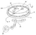
Translated fromKorean도 1a 는 듀얼보트와 기판홀더가 마련되어 백사이드 증착을 방지시키는 반도체 제조장치를 나타낸 개념도,1A is a conceptual diagram illustrating a semiconductor manufacturing apparatus having a dual boat and a substrate holder to prevent backside deposition;
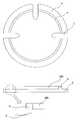
도 1b 는 반도체 제조장치에 적용되는 종래 기판홀더를 나타낸 개념도,1B is a conceptual diagram illustrating a conventional substrate holder applied to a semiconductor manufacturing apparatus;
도 2a 는 본 발명에 따른 반도체 제조장치 기판홀더의 제1실시예를 나타낸 사시설명도,2A is a facility name diagram showing a first embodiment of a semiconductor device substrate holder according to the present invention;
도 2b 는 제1실시예의 단면설명도로서, 도 2a 의 A-A 선 단면설명도,FIG. 2B is a cross-sectional explanatory diagram of the first embodiment, A-A cross-sectional explanatory diagram of FIG. 2A;
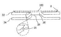
도 3a 는 본 발명에 따른 반도체 제조장치 기판홀더의 제2실시예를 나타낸 사시설명도,FIG. 3A is a private facility diagram showing a second embodiment of a semiconductor device substrate holder according to the present invention; FIG.
도 3b 는 제2실시예의 단면설명도로서, 도 3a 의 B-B 선 단면설명도,3B is a cross-sectional explanatory diagram of the second embodiment, taken along line B-B in FIG. 3A;
도 3c 는 제2실시예의 가스유입 차단면의 다른예를 나타낸 단면설명도,3C is an explanatory cross-sectional view showing another example of the gas inlet blocking surface of the second embodiment;
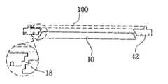
도 4a 는 본 발명에 따른 반도체 제조장치 기판홀더의 제3실시예를 나타낸 사시설명도,4A is a private facility diagram showing a third embodiment of a semiconductor device substrate holder according to the present invention;
도 4b 는 제3실시예의 단면설명도로서, 도 4a 의 C-C 선 단면설명도,4B is a cross-sectional explanatory diagram of the third embodiment, which is taken along line C-C in FIG. 4A;
도 4c 는 제3실시예의 가스 유입차단면의 다른예를 나타낸 단면설명도이다.4C is an explanatory cross-sectional view showing another example of the gas inlet blocking surface of the third embodiment.
- 도면의 주요부분에 대한 부호의 설명 --Explanation of symbols for the main parts of the drawings-
100 - 반도체 기판,3 - 제1기판 로딩용보트,100-semiconductor substrate, 3-first substrate loading boat,
4 - 제2기판 로딩용보트,8 - 기판 측부 가드부,4-2nd substrate loading boat, 8-board side guard,
9 - 듀얼보트,10 - 홀더본체,9-dual boat, 10-holder body,
12 - 기판승강구,14 - 가스유입 차단면,12-substrate hatch, 14-gas inlet barrier,
16 - 테이퍼면,18 - 절곡계단면,16-tapered surface, 18-bending section,
20 - 지지봉,22 - 관통홀,20-support rod, 22-through hole,
24 - 승강로드,26,28 - 기판지지부,24-lifting rod, 26,28-substrate support,
30 - 삽착홈,32 - 상부 홀더본체,30-insert groove, 32-upper holder body,
34 - 하부 홀더본체,36 - 절개부,34-lower holder body, 36-incision,
38 - 돌출턱부,40,48 - 열개부,38-protruding jaw, 40,48-dehiscence,
42 - 기판승강지지대,44 - 결합홀,42-substrate lifting support, 44-coupling hole,
46 - 결합핀,46-coupling pin,
본 발명은 반도체 제조장치의 기판홀더에 관한 것으로, 구체적으로는 듀얼보트가 사용되어 기판홀더를 통해 백사이드 증착을 방지시킨 반도체 제조장치에 있어서 공정시 반도체 기판이 공정반응에 노출되는 것을 원천적으로 방지시킴으로써, 반도체 제조 수율과 생산성을 더욱 향상시킨 반도체 제조장치의 기판홀더에 관한 것이다.BACKGROUND OF THE
일반적으로 반도체 기판을 공정처리하는 반도체 제조장치는 공정 처리능력을 향상시키기 위해서 내부에 반도체 기판을 다량으로 로딩하기 위한 기판 로딩용 보트를 포함하는 배치식과 공정시간을 극도로 감소시키기 위해 한 장씩 공정을 진행하는 매엽식이 있다.In general, a semiconductor manufacturing apparatus for processing a semiconductor substrate is a batch type including a substrate loading boat for loading a large amount of the semiconductor substrate therein to improve the process processing capability and one by one to reduce the process time extremely There is an ongoing single leaf type.
그러나, 종래의 배치식 반도체 제조장치는 공정을 진행할 때 슬롯이 반도체 기판의 가장자리 부분을 국부적으로 거치하고 있기 때문에, 예를 들어 막형성을 하는 공정 중에 반도체 기판의 양면 및 반도체 기판의 하부를 지지하는 로딩용 보트 및 슬롯들 등에도 모두 반도체 공정용 막이 형성된다.However, in the conventional batch type semiconductor manufacturing apparatus, since the slots are locally mounted at the edges of the semiconductor substrate during the process, for example, both sides of the semiconductor substrate and the lower part of the semiconductor substrate are supported during the film forming process. The film for the semiconductor process is also formed in the loading boats and the slots.
따라서, 반도체 제조용 막 공정이 완료된 후 기판을 언로딩시킬때, 기판과 슬롯에 일체로 연결된 막이 파쇄되며, 파쇄시 파티클이 발생되고 기판의 백사이드에는 비교적 많은 파티클이 발생된다.Therefore, when the substrate is unloaded after the semiconductor fabrication process is completed, the film integrally connected to the substrate and the slot is crushed, particles are generated during the crushing, and relatively many particles are generated at the backside of the substrate.
또한, 여러가지 막이 뒷면에 중첩되어 입혀지기 때문에, 기계적 스트레스가 점점 더해져 반도체 기판이 휘는 현상이 발생됨과 더불어, 반도체 기판 백사이드의 막 균일성은 상면의 막 균일성에 비해 현저히 감소하기 때문에 후속공정, 특히 사진공정(Photolithography)에 많은 공정 문제를 발생시킨다.In addition, since various films are overlapped and coated on the back surface, mechanical stress increases and the semiconductor substrate is warped, and the film uniformity of the semiconductor substrate backside is significantly reduced compared to the film uniformity of the upper surface. Photolithography causes many process problems.
이에 본 출원인은 반도체 제조용 막형성 공정 중 반도체 기판의 후면(백사이드)에 막의 생성을 근본적으로 차단시켜, 수율을 향상시키고 전체 반도체 제조공정의 생산성을 대폭 향상 시키는 반도체 제조장치(출원번호 10-2003-0091246)를 출원한바 있다.Therefore, the present applicant essentially blocks the formation of a film on the backside (backside) of the semiconductor substrate during the film forming process for semiconductor manufacturing, thereby improving the yield and significantly improving the productivity of the entire semiconductor manufacturing process (Application No. 10-2003- 0091246).
이것은 예시도면 도 1a 와 같이, 반도체 기판에 막형성 공정을 진행할 수 있 도록 밀폐된 공간을 제공하는 반응튜브(1)와: 반응튜브 내의 공정 공간 내에 장착되어 적어도 하나의 반도체 기판(100)을 로딩할 수 있으며 반도체 기판(100)의 백사이드가 증착되지 않도록 지지하는 기판홀더(2)를 지지하는 제1기판 로딩용 보트(3)와 이 제1기판 로딩용 보트(3)의 내측 또는 외측으로 인접하여 제1기판 로딩용 보트(3)에 대해서 상하로 미세하게 움직일 수 있도록 구성되며 반도체 기판의 가장자리 부분을 독립적으로 지지하는 기판지지대를 포함하는 제2기판 로딩용 보트(4)로 구성된 기판 로딩용 듀얼보트(9)와: 이 기판 로딩용 듀얼보트(9)의 하부에 설치되어 제1기판 로딩용 보트(3) 및 제2기판 로딩용 보트(4)의 하부를 각각 독립적으로 지지하면서 제1기판 로딩용 보트와 제2기판 로딩용 보트 중 적어도 어느 하나를 상하로 승강시켜 반도체 기판의 지지 상태를 상대적으로 조절할 수 있는 간격조절장치(5.구동장치)와: 반응챔버 내에 공정에 필요한 적어도 하나의 공정가스를 공급하는 가스공급장치가 포함되어 이루어진 것이다.This is a
여기서, 기판홀더(2)는 예시도면 도 1b 와 같이 실질적으로 원형판상인 홀더본체(6)와: 기판지지부 부분이 중첩되는 부분을 소정의 도형으로 절개하여 형성된 열개부(7)와: 홀더본체(6)의 판면 상에 형성되어 반도체 기판(100)의 측부 가장자리 부분을 거의 밀착하여 공정가스가 통하지 못하도록 형성된 기판 측부가드부(8)를 포함하며, 기판 측부가드부(8)는 반도체 기판(100)의 가장자리 끝부분을 따라서 홀더본체(6)의 판면으로부터 반도체 기판(100)의 두께 높이만큼 돌출 형성되는 일종의 링형으로 형성된 것이다.Here, the
이러한 기판홀더(2)와 이 기판홀더(2)가 적용되는 듀얼보트(9)를 갖는 반도 체 제조장치를 통해 반도체 기판(100)의 후면에는 반도체 막이 형성되지 않으므로, 반도체 기판의 후면에 증착되는 만도체 막으로 인하여 후속공정에서 발생되는 공정불량을 근본적으로 차단할 수 있는 것이다.Since the semiconductor film is not formed on the rear surface of the
그런데, 상기 기판홀더(2)를 통하여도 반도체 기판이 미세하게 노출되는 부위가 존재하며, 이것은 바로 제2기판로딩용보트(4)의 기판지지부를 승강시키기 위하여 형성된 천공부위인 열개부(7)이다.By the way, there is a portion where the semiconductor substrate is finely exposed through the
즉, 공정완료 후 반도체 기판(100)을 듀얼보트(9)에 언로딩/로딩하기 위하여 반도체 기판(100)은 기판홀더(2)로부터 이격되어야 하고, 공정진행중에도 기판홀더로부터 이격시킬 필요가 있는 관계로, 기판홀더와의 간섭을 회피하여 제2기판로딩용보트가 조합되어 있으며, 제2기판로딩보트의 동작을 위해 열개부(7)가 형성되어 있다.That is, in order to unload / load the
이 열개부(7)에 의해 반도체 기판(100)의 미세구역이 공정에 노출되어 있으며, 공정진행 중 이 미세구역에 공정막이 형성될 우려를 전혀 배제할 수는 없는 것이다.The
이에 본 발명은 듀얼보트가 사용되어 기판홀더를 통해 백사이드 증착을 방지시킨 반도체 제조장치에 있어서 공정시 반도체 기판이 공정반응에 노출되는 것을 원천적으로 방지시킴으로써, 반도체 제조 수율과 생산성을 더욱 향상시킨 반도체 제조장치의 기판홀더를 제공함에 그 목적이 있는 것이다.Accordingly, in the present invention, in the semiconductor manufacturing apparatus in which the dual boat is used to prevent backside deposition through the substrate holder, the semiconductor substrate is prevented from being exposed to the process reaction during the process, thereby further improving semiconductor manufacturing yield and productivity. It is an object to provide a substrate holder of the device.
이를 위한 본 발명은 반도체 기판에 공정을 진행할 수 있도록 밀폐된 공간을 제공하는 반응튜브가 마련되고, 이 반응튜브가 제공하는 공정공간 내에 장착되어 적어도 하나의 반도체 기판이 로딩되며 상호 상하로 이동되는 제1기판 로딩용 보트와 제2기판 로딩용 보트에 의해 간격이 제공되는 듀얼보트가 마련됨과 더불어, 이 듀얼보트에 반도체 기판이 안착되는 기판홀더가 안착되어져 공정진행 중 반도체 기판의 후면이 은폐되는 반도체 제조장치의 기판홀더에 있어서:The present invention for this purpose is provided with a reaction tube for providing a closed space to proceed the process on the semiconductor substrate, is mounted in the process space provided by the reaction tube at least one semiconductor substrate is loaded and moved up and down with each other A dual boat is provided with a gap provided by a first board loading boat and a second board loading boat, and a substrate holder on which the semiconductor substrate is seated is seated on the dual boat, thereby concealing the rear surface of the semiconductor substrate during the process. In the substrate holder of the manufacturing apparatus:
상기 기판홀더는 밀폐된 공정공간을 제공하는 반응튜브 내에서 공정진행 중 반도체 기판의 후면이 은폐되도록 홀더본체가 마련되고, 반도체 기판의 로딩/언로딩 시에는 홀더본체로부터 반도체 기판이 듀얼보트를 통해 저부가 지지되어 승강되게 상기 홀더본체에는 그 일부가 홀더본체에서 분리 결합되는 기판승강구가 형성됨과 더불어, 이 홀더본체와 기판승강구의 분리 경계부에는 여기로부터의 반응가스 유입이 방해되게 가스유입 차단면이 형성되어 맞물리게 분리결합되는 것을 특징으로 하는 반도체 제조장치의 기판홀더이다.The substrate holder is provided with a holder body so that the rear surface of the semiconductor substrate is concealed during the process in the reaction tube that provides a closed process space, the semiconductor substrate from the holder body through the dual boat during loading / unloading of the semiconductor substrate The holder body is formed so that the bottom part is supported and lifted, and the substrate lifting hole is formed to be separated from the holder body. It is a substrate holder of the semiconductor manufacturing apparatus, characterized in that the engagement is separated.
상기 가스유입 차단면은 서로 대향되는 테이퍼면이나, 연속되어 절곡된 절곡계단면 또는 이들이 조합되어 홀더본체와 기판승강구가 결합된 공정진행 중 경계면으로부터의 반응가스 유입을 차단한다.The gas inlet blocking surface is a tapered surface facing each other, a continuously bent section surface or a combination thereof to block the inlet of the reaction gas from the interface during the process of combining the holder body and the substrate lifting hole.
상기 기판승강구에 의해 본 발명의 홀더본체는 다수의 실시예로 구분되며, 제1의 실시예로서 기판승강구는 홀더본체의 측부가드부 내측에 반도체 기판을 적어도 3점 지지하는 지지봉으로 마련되고 홀더본체에는 상기 지지봉이 삽탈되는 관통홀이 형성되며, 이 지지봉의 저부에는 듀얼보트의 제2기판로딩용보트에 의해 작동 되는 승강로드가 배치된 것을 특징으로 한다.The holder body of the present invention is divided into a plurality of embodiments by the substrate hatch, and as a first embodiment, the substrate hatch is provided with a supporting rod for supporting at least three points of the semiconductor substrate inside the side guard portion of the holder body, and the holder body. There is formed a through hole through which the supporting rod is inserted and removed, characterized in that the bottom of the supporting rod is provided with a lifting rod which is operated by the second board loading boat of the dual boat.
여기서, 승강로드는 그 저부에 삽착홈이 형성되고 이 삽착홈에 제2기판 로딩용보트의 기판지지부의 단부가 삽착되어 결합되는 것을 특징으로 한다.Here, the lifting rod is characterized in that the insertion groove is formed at the bottom thereof, the end portion of the substrate support of the second substrate loading boat is inserted into the insertion groove is coupled.
또한, 변형례로는 제2기판로딩용보트에 대체되어 별도의 로봇아암이 배치되고 이 로봇아암에 승강로드가 포함되어 지지봉을 승강시키는 것을 특징으로 한다.In addition, as a modification, a separate robot arm is disposed in place of the second substrate loading boat, and a lifting rod is included in the robot arm to lift the supporting rod.
한편, 제2의 실시예로서 기판승강구는 홀더본체가 상하로 2분할되고 제2기판로딩용 보트에 의해 작동되는 상부 홀더본체는 최소한 반도체 기판을 승강시키면서 반도체 기판의 로딩/언로딩을 위한 로봇아암의 삽입면적을 제공하는 구역으로 절개부가 형성되고, 제1기판 로딩용 보트에 장착되는 하부홀더본체에는 상기 상기 절개부에 맞물리는 돌출턱부가 형성됨과 더불어 그 외주부에는 상기 제2기판 로딩용 보트를 통해 상기 상부홀더본체의 승강이 수행되게 열개부가 형성된 것을 특징으로 한다.On the other hand, in the second embodiment, the substrate lifting hole includes a robot arm for loading / unloading the semiconductor substrate while the holder body is divided into two vertically and the upper holder body operated by the second substrate loading boat at least while lifting the semiconductor substrate. An incision is formed into an area providing an insertion area of the lower holder body, which is attached to the first substrate loading boat, and has a protruding jaw portion engaged with the incision, and an outer peripheral portion of the boat for loading the second substrate. It is characterized in that the opening portion is formed so that the lifting of the upper holder body through.
다음으로, 제3의 실시예로서 기판승강구는 듀얼보트가 결합되는 홀더본체 부위가 분리되어 제2기판 로딩용보트와 결합되는 기판승강지지대가 형성되며, 이 기판승강지지대는 홀더본체에서 분리되어 적어도 반도체 기판의 외주부를 거치하게 기판 측부 가드부 내측으로 연장되어 형성되는 한편, 제1기판 로딩용보트는 상기 기판승강지지대의 분리가 제공하는 열개부에 이웃하여 홀더본체를 거치시키는 것을 특징으로 한다.Next, as a third embodiment, the substrate lifting hole is separated from the holder body portion to which the dual boat is coupled to form a substrate lifting support coupled with the second substrate loading boat, and the substrate lifting support is separated from the holder body. While extending to the inside of the substrate side guard portion so as to mount the outer peripheral portion of the semiconductor substrate, the first substrate loading boat is characterized in that the holder body is mounted adjacent to the opening provided by the separation of the substrate lifting support.
여기서, 기판승강구본체는 그 저부와 제2기판 로딩용보트의 지지부 중 어느 하나에 결합홀이 형성되고 다른 하나에 이 결합홀과 삽착되는 결합핀이 형성되어 기판승강구본체와 제2기판 로딩용보트가 결합되는 것을 특징으로 한다.Here, the substrate lifting body has a coupling hole is formed in any one of the bottom portion and the support portion of the second substrate loading boat, the coupling pin is inserted into the coupling hole and inserted into the other board, the substrate lifting body and the second substrate loading boat It is characterized in that the combined.
이하, 이 발명이 속하는 기술분야에서 통상의 지식을 갖는 자가 이 발명을 용이하게 실시할 수 있을 정도로 상세히 설명하기 위하여, 이 발명의 가장 바람직한 실시예를 첨부된 도면을 참조로 하여 상세히 설명하기로 한다. 이 발명의 목적, 작용효과를 포함하여 기타 다른 목적들, 특징점들, 그리고 동작상의 이점들이 바람직한 실시예의 설명에 의해 보다 명확해질 것이다.DETAILED DESCRIPTION Hereinafter, the most preferred embodiments of the present invention will be described in detail with reference to the accompanying drawings so that those skilled in the art can easily implement the present invention. . Other objects, features, and operational advantages, including the purpose, working effects, and the like of the present invention will become more apparent from the description of the preferred embodiment.
참고로 여기에서 개시되는 실시예는 여러가지 실시가능한 예 중에서 당업자의 이해를 돕기 위하여 가장 바람직한 예를 선정하여 제시한 것일뿐, 이 발명의 기술적 사상이 반드시 이 실시예에 의해서 한정되거나 제한되는 것은 아니고, 본 발명의 기술적 사상을 벗어나지 않는 범위내에서 다양한 변화와 변경이 가능함은 물론, 균등한 타의 실시예가 가능함을 밝혀 둔다.For reference, the embodiments disclosed herein are only presented by selecting the most preferred examples to help those skilled in the art from the various possible examples, the technical spirit of the present invention is not necessarily limited or limited by this embodiment, Various changes and modifications are possible within the scope without departing from the technical spirit of the present invention, as well as other equivalent embodiments will be found.
먼저, 본 발명의 기판홀더는 도시된 링형의 기판홀더에 국한되지 않음을 밝혀둔다.First, it should be noted that the substrate holder of the present invention is not limited to the ring-shaped substrate holder shown.
특히, 기판 측부 가드부는 본 발명을 설명을 위하여 링형으로 이루어진 하나의 예를 나타내었을 뿐이고, 본 발명은 기판홀더 본체에 관련된 것으로 다른 측부가드를 나타낸 테이퍼형이나 포켓타입의 기판홀더에도 본 발명이 적용되어짐은 당연하다.Particularly, the substrate side guard portion merely shows one example made of a ring shape for explaining the present invention, and the present invention relates to a substrate holder main body, and the present invention also applies to a tapered or pocket type substrate holder showing another side guard. It is natural.
예시도면 도 2 내지 도 4 는 본 발명에 따른 반도체 기판홀더의 각 실시예를 나타낸 사시설명도와 그 작동상태를 나타낸 개념도로서, 본 발명은 반도체 기판에 공정을 진행할 수 있도록 밀폐된 공간을 제공하는 반응튜브가 마련되고, 이 반응튜 브가 제공하는 공정공간 내에 장착되어 적어도 하나의 반도체 기판(100)이 로딩되며 상호 상하로 이동되는 제1기판 로딩용보트(3)와 제2기판 로딩용보트(4)에 의해 간격이 제공되는 듀얼보트가 마련됨과 더불어, 이 듀얼보트에 반도체 기판이 안착되는 기판홀더(2)가 안착되어져 공정진행 중 반도체 기판의 후면이 은폐되는 반도체 제조장치의 기판홀더에 있어서:2 to 4 is a conceptual diagram showing the company name and the operating state of each embodiment of the semiconductor substrate holder according to the present invention, the present invention is a reaction for providing a closed space to proceed the process to the semiconductor substrate A first
상기 기판홀더는 밀폐된 공정공간을 제공하는 반응튜브 내에서 공정진행 중 반도체 기판의 후면이 은폐되도록 홀더본체(10)가 마련되고, 반도체 기판(100)의 로딩/언로딩 시에는 홀더본체(10)로부터 반도체 기판이 듀얼보트(9)를 통해 저부가 지지되어 승강되게 상기 홀더본체(10)에는 그 일부가 홀더본체(10)에서 분리 결합되는 기판승강구(12)가 형성됨과 더불어, 이 홀더본체(10)와 기판승강구(12)의 분리 경계부에는 여기로부터의 반응가스 유입이 방해되게 가스유입 차단면(14)이 형성되어 맞물리게 분리결합되는 것을 특징으로 하는 반도체 제조장치의 기판홀더이다.The substrate holder is provided with a
이러한 본 발명의 각 실시예에 있어서, 공통적으로 상기 가스유입 차단면(14)은 홀더본체(10)와 기판승강구(12)가 결합된 공정진행 중 경계면으로부터의 반응가스 유입을 차단하게 기판승강구와 홀더본체가 서로 대향되는 테이퍼면(16)으로 맞물리게 분리결합되는 것을 특징으로 한다.In each of the embodiments of the present invention, the gas
또한, 상기 가스유입 차단면(14)은 홀더본체(10)와 기판승강구(12)가 결합된 공정진행 중 경계면으로부터의 반응가스 유입을 차단하게 기판승강구와 홀더본체가 연속되어 절곡된 절곡계단면(18)으로 맞물리게 분리결합되는 것을 특징으로 한다.In addition, the gas
이러한 본 발명은 상기 기판승강구에 의해 각 실시예로 구분되며, 이 중 예시도면 도 2 는 본 발명에 따른 반도체 제조장치 기판홀더의 제1의 실시예를 나타낸 도면이다.The present invention is divided into each embodiment by the substrate lifting hole, an exemplary view of which Figure 2 is a view showing a first embodiment of a substrate holder of the semiconductor manufacturing apparatus according to the present invention.
즉 제1실시예로서 기판홀더의 기판승강구(12)는 홀더본체(10)의 기판 측부 가드부(8) 내측에 반도체 기판(100)을 적어도 3점 지지하는 지지봉(20)으로 마련되고 홀더본체(10)에는 상기 지지봉이 삽탈되는 관통홀(22)이 형성되며, 이 지지봉(20)의 저부에는 제2기판로딩용보트(4)에 의해 작동되는 승강로드(24)가 배치된 것이다.That is, as the first embodiment, the
이것은 캡타입의 기판승강구를 나타내며, 분리된 캡인 지지봉(20)이 기판홀더본체(10)로부터 승강되어져 반도체 기판을 지지하게 된다.This represents a cap-type substrate lifting hole, and the supporting
여기서 캡타입은 상기 지지봉(20)과 관통홀(22)에 가스유입 차단면(14)으로서 테이퍼면이나 절곡계단면이 형성되어 그 단면형상의 변형이 있기 때문이다.The cap type is because the taper surface or the bending section surface is formed as the gas
이러한 캡타입의 기판승강구는 홀더본체(10)의 기판 측부 가드부(8) 내측에 마련되므로, 기판 측부 가드부(8)와 연동되어 공정진행시 반도체 기판(100)의 후면이 공정에 노출되는 것을 원천적으로 방지시키게 된다.Since the cap-type substrate lifting hole is provided inside the substrate
즉, 공정진행을 위해 홀더본체(10)에 반도체 기판(100)이 안착되면, 측부는 기판 측부 가드부(8)에 의해 은폐되고, 그 저부는 홀더본체(10)에 의해 은폐됨과 더불어, 가스유입 차단면(14)은 지지봉(20)과 기판홀더 본체의 결합 경계면으로부터 가스가 유입되는 것을 방지시키고 있는 것이다.That is, when the
이때, 홀더본체(10)는 제1기판 로딩용보트(3)의 기판지지부(26)에 거치되어 있고, 상기 지지봉(20)의 저부에는 승강로드(24)가 배치되며, 승강로드(24)는 제2기판 로딩용보트(4)의 기판지지부(28)에 결합되어 있다.At this time, the
여기서, 승강로드(24)는 원형일 수도 있으며 그 저부에 삽착홈(30)이 형성되고 이 삽착홈(30)에 제2기판 로딩용보트(4)의 기판지지부(28)의 단부가 삽착되어 결합되는 것을 특징으로 한다.Here, the lifting
이러한 제1실시예에 따라, 공정진행 중에는 반도체 기판(100)의 상면만이 노출되어 공정이 진행되므로, 반도체 기판(100) 후면의 증착이 원천적으로 방지되는 것이다.According to the first embodiment, since only the top surface of the
다음으로, 반도체 기판(100) 언로딩/로딩시에 로봇암의 작동을 위해서는 홀더본체(10)로부터 반도체 기판(100)이 이격되어야 하며, 이때 제2기판 로딩용보트(4)가 상승되면서 기판지지부(28)가 승강로드(24)를 상승시키고, 이에 의해 지지봉(20)은 반도체 기판(100)을 상승시키게 되는 것이다.Next, in order to operate the robot arm during the unloading / loading of the
이러한 본 발명에서는 듀얼보트에 있어서, 제1기판 로딩용 보트 및 제2기판 로딩용보트의 슬릿이나 기판지지부의 설계자유도를 갖게된다.In the present invention, in the dual boat, the first substrate loading boat and the second substrate loading boat have slit or substrate support part design freedom.
이것은 특히 제2기판로딩용보트의 기판지지부가 직접 반도체기판과 접촉되지 아니하고, 미세접촉면적이 고려된 종래 열개부 확보가 필요치 않기 때문이다.This is because the substrate supporting portion of the second substrate loading boat is not directly in contact with the semiconductor substrate, and it is not necessary to secure the conventional ten parts considering the microcontact area.
이러한 이유로, 본 발명에서 특히 제1기판로딩용보트와 제2기판로딩용보트의 기판지지부의 어느 정도 변경이 허락되며, 그 자유도에 의해 상세설명은 생략한다.For this reason, in the present invention, a change of the substrate support portion of the first substrate loading boat and the second substrate loading boat is allowed to some extent, and the detailed description thereof is omitted by the degree of freedom.
다만, 제1의 실시예에서는 간격 배치상 제2기판로딩용보트가 로봇아암으로 대체될 수 있다.However, in the first embodiment, the second substrate loading boat may be replaced by the robot arm in the interval arrangement.
이것은 제1의 실시예에서 지지봉을 밀어내기 위하여 하부에 반도체기판의 언로딩시 로봇암이 작동될 공간을 제공하는 필요길이를 갖는 승강로드가 필요하고 승강로드의 두께와 기판홀더 저부에서의 소정의 이격길이와 더불어, 반응가스의 유동을 위한 필요 공간부를 감안하고, 로딩/언로딩시 로봇아암의 필요작업공간부를 감안할 때, 배치형 반도체 제조장치에서 반도체 기판의 배열간격이 멀어질 우려가 있기 때문이다.In the first embodiment, this requires a lifting rod having a required length that provides space for the robot arm to be operated when unloading the semiconductor substrate in order to push out the supporting rod, and the thickness of the lifting rod and the predetermined thickness at the bottom of the substrate holder. In addition to the separation length, considering the required space for the flow of the reaction gas, and considering the required working space of the robot arm during loading and unloading, there is a possibility that the arrangement interval of the semiconductor substrate in the batch type semiconductor manufacturing apparatus may be far apart. to be.
따라서, 본 발명의 제1실시예에서 승강작동구는 제2기판로딩용 보트에 대체되어 별도의 로봇아암(미도시)이 배치되고 이 로봇아암에 승강로드가 포함되어 지지봉을 승강시키는 것을 특징으로 한다.Therefore, in the first embodiment of the present invention, the lifting operation tool is replaced with a boat for loading the second substrate, and a separate robot arm (not shown) is disposed, and the lifting arm is included in the robot arm to lift the supporting rod. .
다음으로, 예시도면 도 3 은 본 발명에 따른 반도체 제조장치 기판홀더의 제2의 실시예를 나타낸 사시설명도와 단면설명도로서, 제2의 실시예로서 기판홀더의 기판승강구(12)는 홀더본체(10)가 상하로 2분할되어 제2기판 로딩용보트(4)에 의해 작동되는 상부 홀더본체(32)는 최소한 반도체 기판(10)을 승강시키면서 반도체 기판(100)의 로딩/언로딩을 위한 로봇아암의 삽입면적을 제공하는 구역으로 절개부(36)가 형성되고, 제1기판 로딩용보트(3)에 장착되는 하부 홀더본체(34)에는 상기 상기 절개부(36)에 맞물려 이 절개부에 연장되어 기판홀더형상을 이루도록 돌출턱부(38)가 형성됨과 더불어 그 외주부에는 상기 제2기판 로딩용보트(4)의 기판지지부(28)를 통해 상기 상부 홀더본체(32)의 승강이 수행되게 열개부(40)가 형성된 것을 특징으로 한다.Next, FIG. 3 is a perspective view and a cross-sectional explanatory view showing a second embodiment of the semiconductor manufacturing apparatus substrate holder according to the present invention. As a second embodiment, the
이것은 제1실시예와는 달리 제1실시예의 승강로드를 분할된 하부 홀더본체(34)가 담당하게 되며, 하부 홀더본체(34)와 상부 홀더본체(32)는 공정진행시 서로 밀접되므로, 기판홀더의 배치간격을 좀 더 감소시키게 된다.Unlike the first embodiment, the lower holder
이를 위한 상부 홀더본체(32)에는 반도체 기판(100)이 안착되어 이를 승강시키는 면적과 더불어, 로봇아암의 작동공간을 제공하는 절개부(36)가 형성되며, 하부 홀더본체(34)에는 이 절개부(36)를 연장하여 기판홀더형상을 이루는 돌출턱부(38)가 형성되어 있다.The
그리고, 하부 홀더본체(34)에는 기판 측부 가드부(8) 외측으로 열개부(40)가 형성되어, 하부 홀더본체(34)는 제1기판 로딩용보트(3)의 기판지지부(26)에 거치되고, 열개부(40)를 통해 상부 홀더본체(32)가 제2기판 로딩용보트(4)의 기판지지부(28)에 거치된다.In addition, the
따라서, 공정진행 중에는 상부 홀더본체(32)와 상부 홀더본체의 절개부를 감당하는 하부 홀더본체의 돌출턱부(38)에 의해 반도체 기판(100)의 상면만이 공정에 노출된다.Therefore, during the process, only the upper surface of the
뒤이어 반도체 기판의 언로딩/로딩시에는 제2기판 로딩용보트(4)가 승강되고, 이것의 기판지지부(28)는 열개부(40)를 통해 승강되며, 이에 의해 상부 홀더본체(32)가 승강되어 절개부(36)가 공개된다.Subsequently, during the unloading / loading of the semiconductor substrate, the second
이 절개부(36)를 통해 로봇아암이 반도체 기판(100)의 언로딩/로딩을 수행하게 된다.Through the
한편, 예시도면 도 3c 는 가스유입 차단면의 다른 적용예를 나타낸 단면설명도로서, 전술된 바와 같이 가스유입 차단면(14)은 분리된 두부재 사이의 경계틈으 로부터 반응가스가 유입되는 것을 방지시키기 위하여 형성된 것으로, 도 3b의 테이퍼면(16)으로 형성되거나, 절곡된 절곡계단면(18)으로 형성되면 충분하며, 이 두가지 형태가 조합되어도 무방하다.On the other hand, Figure 3c is a cross-sectional explanatory view showing another application example of the gas inlet blocking surface, as described above the gas
다음으로, 예시도면 도 4 는 본 발명의 반도체 제조장치 기판홀더의 제3실시예를 나타낸 사시설명도와 단면설명도로서, 제3의 실시예로서 기판승강구(12)는 듀얼보트(9)가 결합되는 홀더본체(10) 부위가 분리되어 제2기판 로딩용보트(4)의 기판지지부(28)와 결합되는 기판승강지지대(42)가 형성되며, 이 기판승강지지대(42)는 홀더본체(10)에서 분리되어 적어도 반도체 기판(100)의 외주부를 거치하게 기판 측부 가드부(8) 내측으로 연장되어 형성되는 한편, 제1기판 로딩용보트(3)는 상기 기판승강지지대(42)의 측부에 이웃하여 홀더본체(10)를 거치시키는 것을 특징으로 한다.Next, Figure 4 is a facility name and a cross-sectional explanatory view showing a third embodiment of the semiconductor manufacturing apparatus substrate holder of the present invention, the
여기서, 기판승강지지대(42)는 그 저부와 제2기판 로딩용보트(4)의 기판지지부(28) 중 어느 하나에 결합홀(44)이 형성되고 다른 하나에 이 결합홀(44)과 삽착되는 결합핀(46)이 형성되어 기판승강지지대와 제2기판 로딩용보트가 결합되는 것을 특징으로 한다.Here, the
이것은 제2실시예와는 달리 제2실시예의 상하로 분할되어 형성된 하부 기판홀더본체를 수평으로 분할된 기판승강지지대(42)가 담당하게 되며, 홀더본체(10)와 기판승강지지대(42)는 수평으로 배치되므로, 하나의 기판홀더 두께만이 소요되므로 기판홀더의 배치간격을 더욱 감소시키게 된다.Unlike the second embodiment, the lower and lower substrate holder body formed by dividing the upper and lower parts of the second embodiment is in charge of the
이를 위한 기판승강지지대(42)는 마치 홀더본체(10)에 열개부(48)가 충진되 어져 분리된 형상이며, 기판승강지지대(42)의 일부는 기판 측부 가드부(8) 내측으로 연장되어 반도체기판의 외주저부와 접촉되도록 마련되어 있다.
그리고, 이 기판승강지지대(42)가 제2기판 로딩용보트(4)의 기판지지부(28)와 결합되며, 제1기판 로딩용보트(3)의 기판지지부(26)는 이기판승강지지대(42)가 제공하는 열개부(48)와 이웃하여 홀더본체(10) 저부를 거치하도록 마련되어 있다.Then, the
따라서, 공정진행 중에는 기판승강지지대(42)와 홀더본체(10)가 결합되어 반도체 기판(100)의 상면만이 공정에 노출된다.Therefore, during the process, the
뒤이어, 반도체 기판(100)의 언로딩/로딩시에는 제2기판 로딩용보트(4)의 기판지지부(28)가 상승되고, 이에 결합된 기판승강지지대(42)가 상승되면서 반도체 기판(100)이 상승되고, 로봇아암이 작업을 수행하게 되는 것이다.Subsequently, during unloading / loading of the
한편, 기판승강지지대(42)와 홀더본체(10)는 상협하광의 가스유입 차단면(14)을 갖으며, 예시도면 도 4c 는 가스유입 차단면의 다른 예로서 상술된 바와 같이 절곡계단면(18)을 갖는 가스유입 차단면을 나타내고 있다.On the other hand, the
이러한 본 발명의 각 실시예를 통하여 배치식 반도체 제조장치에 있어서, 다량의 반도체 기판이 로딩되면서도 반도체 기판의 상면만을 공정에 노출시켜 반도체 기판의 백사이드(후면)의 막형성을 원천적으로 방지시키게 되는 것이다.In the batch type semiconductor manufacturing apparatus through each embodiment of the present invention, even when a large amount of the semiconductor substrate is loaded, only the top surface of the semiconductor substrate is exposed to the process to prevent the film formation of the backside (back side) of the semiconductor substrate at the source. .
상기 각 실시예는 각각 독특한 장점이 부각된 것으로, 예를 들어 제1실시예와 제3실시예를 비교해 보면 제1실시예는 지지봉이 기판 측부가드부 내측에 배치되어 반도체 기판의 노출이 원천적으로 방지되는 대신 승강로드에 의해 반도체 기판의 배치간격이 증가되며, 제3실시예에서는 기존의 반도체 기판 배치간격을 충분히 유지시키면서도 기존라인의 최소한 변경으로 적용이 가능한 대신 기판승강지지대의 형성에 따라 기판측부가드부에 절개선이 발생되며 절개선의 정밀한 틈 조절이 필요할 것이다.Each of the above-mentioned embodiments has a unique advantage. For example, in comparison with the first and third embodiments, the first embodiment has a support rod disposed inside the side-side portion of the substrate, thereby exposing the semiconductor substrate. Instead of being prevented, the lifting interval of the semiconductor substrate is increased by the lifting rod, and in the third embodiment, it is possible to apply a minimum change of the existing line while sufficiently maintaining the existing semiconductor substrate arrangement interval, but instead, the substrate side part is formed according to the formation of the substrate lifting support. An incision will be created in the guard and will require precise clearance control.
상술된 바와 같이 본 발명에 따르면, 가스유입 차단면이 포함되고 기판홀더의 일부분이 분리되어 기판승강구가 형성됨으로써, 종래 열개부에 의한 반도체 기판의 공정노출이 원천적으로 방지되므로, 반도체의 제조수율과 생산성이 더욱 향상되는 효과가 있다.As described above, according to the present invention, since the gas inlet blocking surface is included and a part of the substrate holder is separated to form the substrate hatch, the process exposure of the semiconductor substrate is prevented by the dehisable portion of the prior art. Productivity is further improved.
Claims (9)
Translated fromKoreanPriority Applications (4)
| Application Number | Priority Date | Filing Date | Title |
|---|---|---|---|
| KR1020040003072AKR100549273B1 (en) | 2004-01-15 | 2004-01-15 | Substrate Holder of Semiconductor Manufacturing Equipment |
| US10/839,711US7207763B2 (en) | 2004-01-15 | 2004-05-06 | Semiconductor manufacturing system and wafer holder for semiconductor manufacturing system |
| DE102004022933ADE102004022933A1 (en) | 2004-01-15 | 2004-05-10 | Wafer holder for semiconductor manufacturing system, has holder body with lifter disengaged from and coupled to body so that lower portion of wafer is supported by dual boat and to lift wafer from wafer body when wafer is loaded or unloaded |
| JP2004145449AJP3988948B2 (en) | 2004-01-15 | 2004-05-14 | Semiconductor manufacturing equipment |
Applications Claiming Priority (1)
| Application Number | Priority Date | Filing Date | Title |
|---|---|---|---|
| KR1020040003072AKR100549273B1 (en) | 2004-01-15 | 2004-01-15 | Substrate Holder of Semiconductor Manufacturing Equipment |
Publications (2)
| Publication Number | Publication Date |
|---|---|
| KR20050075140A KR20050075140A (en) | 2005-07-20 |
| KR100549273B1true KR100549273B1 (en) | 2006-02-03 |
Family
ID=34747831
Family Applications (1)
| Application Number | Title | Priority Date | Filing Date |
|---|---|---|---|
| KR1020040003072AExpired - Fee RelatedKR100549273B1 (en) | 2004-01-15 | 2004-01-15 | Substrate Holder of Semiconductor Manufacturing Equipment |
Country Status (4)
| Country | Link |
|---|---|
| US (1) | US7207763B2 (en) |
| JP (1) | JP3988948B2 (en) |
| KR (1) | KR100549273B1 (en) |
| DE (1) | DE102004022933A1 (en) |
Families Citing this family (409)
| Publication number | Priority date | Publication date | Assignee | Title |
|---|---|---|---|---|
| US20060113806A1 (en)* | 2004-11-29 | 2006-06-01 | Asm Japan K.K. | Wafer transfer mechanism |
| US8012888B2 (en)* | 2006-02-23 | 2011-09-06 | Hitachi Kokusai Electric Inc. | Substrate processing apparatus and semiconductor device manufacturing method |
| JP4313401B2 (en)* | 2007-04-24 | 2009-08-12 | 東京エレクトロン株式会社 | Vertical heat treatment apparatus and substrate transfer method |
| JP4922870B2 (en)* | 2007-08-31 | 2012-04-25 | 株式会社アルバック | Board lift device |
| JP5548841B2 (en)* | 2008-01-16 | 2014-07-16 | チャーム エンジニアリング シーオー エルティーディー | Substrate processing equipment |
| USD600221S1 (en)* | 2008-03-28 | 2009-09-15 | Tokyo Electron Limited | Wafer boat |
| TWD133942S1 (en)* | 2008-03-28 | 2010-03-21 | 東京威力科創股份有限公司 | Crystal Boat |
| US10378106B2 (en) | 2008-11-14 | 2019-08-13 | Asm Ip Holding B.V. | Method of forming insulation film by modified PEALD |
| US9394608B2 (en) | 2009-04-06 | 2016-07-19 | Asm America, Inc. | Semiconductor processing reactor and components thereof |
| US8802201B2 (en) | 2009-08-14 | 2014-08-12 | Asm America, Inc. | Systems and methods for thin-film deposition of metal oxides using excited nitrogen-oxygen species |
| TW201133700A (en)* | 2009-12-18 | 2011-10-01 | Nikon Corp | Pair of substrate holders, method for manufacturing device, separation device, method for separating substrates, substrate holder, and device for positioning substrate |
| EP2360720A1 (en)* | 2010-02-23 | 2011-08-24 | Saint-Gobain Glass France | Device for positioning at least two objects, assemblies in particular multi-layer body assemblies, assembly for processing, in particular selenization, of objects, method for positioning at least two objects |
| US9312155B2 (en) | 2011-06-06 | 2016-04-12 | Asm Japan K.K. | High-throughput semiconductor-processing apparatus equipped with multiple dual-chamber modules |
| US9793148B2 (en) | 2011-06-22 | 2017-10-17 | Asm Japan K.K. | Method for positioning wafers in multiple wafer transport |
| US10364496B2 (en) | 2011-06-27 | 2019-07-30 | Asm Ip Holding B.V. | Dual section module having shared and unshared mass flow controllers |
| US10854498B2 (en) | 2011-07-15 | 2020-12-01 | Asm Ip Holding B.V. | Wafer-supporting device and method for producing same |
| US20130023129A1 (en) | 2011-07-20 | 2013-01-24 | Asm America, Inc. | Pressure transmitter for a semiconductor processing environment |
| US9017481B1 (en) | 2011-10-28 | 2015-04-28 | Asm America, Inc. | Process feed management for semiconductor substrate processing |
| US8946830B2 (en) | 2012-04-04 | 2015-02-03 | Asm Ip Holdings B.V. | Metal oxide protective layer for a semiconductor device |
| US9558931B2 (en) | 2012-07-27 | 2017-01-31 | Asm Ip Holding B.V. | System and method for gas-phase sulfur passivation of a semiconductor surface |
| US9659799B2 (en) | 2012-08-28 | 2017-05-23 | Asm Ip Holding B.V. | Systems and methods for dynamic semiconductor process scheduling |
| KR101889738B1 (en) | 2012-09-07 | 2018-09-20 | 세메스 주식회사 | Apparatus and Method for processing a substrate |
| US9021985B2 (en) | 2012-09-12 | 2015-05-05 | Asm Ip Holdings B.V. | Process gas management for an inductively-coupled plasma deposition reactor |
| US9324811B2 (en) | 2012-09-26 | 2016-04-26 | Asm Ip Holding B.V. | Structures and devices including a tensile-stressed silicon arsenic layer and methods of forming same |
| US10714315B2 (en) | 2012-10-12 | 2020-07-14 | Asm Ip Holdings B.V. | Semiconductor reaction chamber showerhead |
| US9640416B2 (en) | 2012-12-26 | 2017-05-02 | Asm Ip Holding B.V. | Single-and dual-chamber module-attachable wafer-handling chamber |
| KR102097109B1 (en)* | 2013-01-21 | 2020-04-10 | 에이에스엠 아이피 홀딩 비.브이. | Deposition apparatus |
| US20160376700A1 (en) | 2013-02-01 | 2016-12-29 | Asm Ip Holding B.V. | System for treatment of deposition reactor |
| US9484191B2 (en) | 2013-03-08 | 2016-11-01 | Asm Ip Holding B.V. | Pulsed remote plasma method and system |
| US9589770B2 (en) | 2013-03-08 | 2017-03-07 | Asm Ip Holding B.V. | Method and systems for in-situ formation of intermediate reactive species |
| KR101390474B1 (en)* | 2013-04-08 | 2014-05-07 | 주식회사 유진테크 | Apparatus for processing substrate |
| US8993054B2 (en) | 2013-07-12 | 2015-03-31 | Asm Ip Holding B.V. | Method and system to reduce outgassing in a reaction chamber |
| US9018111B2 (en) | 2013-07-22 | 2015-04-28 | Asm Ip Holding B.V. | Semiconductor reaction chamber with plasma capabilities |
| CN104347460B (en)* | 2013-08-01 | 2017-03-15 | 中微半导体设备(上海)有限公司 | Wafer transmits chamber |
| US9793115B2 (en) | 2013-08-14 | 2017-10-17 | Asm Ip Holding B.V. | Structures and devices including germanium-tin films and methods of forming same |
| US9240412B2 (en) | 2013-09-27 | 2016-01-19 | Asm Ip Holding B.V. | Semiconductor structure and device and methods of forming same using selective epitaxial process |
| US9556516B2 (en) | 2013-10-09 | 2017-01-31 | ASM IP Holding B.V | Method for forming Ti-containing film by PEALD using TDMAT or TDEAT |
| US10179947B2 (en) | 2013-11-26 | 2019-01-15 | Asm Ip Holding B.V. | Method for forming conformal nitrided, oxidized, or carbonized dielectric film by atomic layer deposition |
| US9370863B2 (en)* | 2014-02-04 | 2016-06-21 | Asm Ip Holding B.V. | Anti-slip end-effector for transporting workpiece |
| US10683571B2 (en) | 2014-02-25 | 2020-06-16 | Asm Ip Holding B.V. | Gas supply manifold and method of supplying gases to chamber using same |
| US10167557B2 (en) | 2014-03-18 | 2019-01-01 | Asm Ip Holding B.V. | Gas distribution system, reactor including the system, and methods of using the same |
| US9447498B2 (en) | 2014-03-18 | 2016-09-20 | Asm Ip Holding B.V. | Method for performing uniform processing in gas system-sharing multiple reaction chambers |
| US11015245B2 (en) | 2014-03-19 | 2021-05-25 | Asm Ip Holding B.V. | Gas-phase reactor and system having exhaust plenum and components thereof |
| KR102141855B1 (en)* | 2014-03-31 | 2020-08-07 | 주식회사 선익시스템 | Mask align apparatus |
| US9404587B2 (en) | 2014-04-24 | 2016-08-02 | ASM IP Holding B.V | Lockout tagout for semiconductor vacuum valve |
| TWI653701B (en)* | 2014-06-09 | 2019-03-11 | 日商荏原製作所股份有限公司 | Substrate attaching and detaching portion for substrate holder, wet substrate processing device including the substrate attaching and detaching portion, substrate processing device, and substrate transfer method |
| US10858737B2 (en) | 2014-07-28 | 2020-12-08 | Asm Ip Holding B.V. | Showerhead assembly and components thereof |
| US9543180B2 (en) | 2014-08-01 | 2017-01-10 | Asm Ip Holding B.V. | Apparatus and method for transporting wafers between wafer carrier and process tool under vacuum |
| US9890456B2 (en) | 2014-08-21 | 2018-02-13 | Asm Ip Holding B.V. | Method and system for in situ formation of gas-phase compounds |
| US10941490B2 (en) | 2014-10-07 | 2021-03-09 | Asm Ip Holding B.V. | Multiple temperature range susceptor, assembly, reactor and system including the susceptor, and methods of using the same |
| US9657845B2 (en) | 2014-10-07 | 2017-05-23 | Asm Ip Holding B.V. | Variable conductance gas distribution apparatus and method |
| KR102300403B1 (en) | 2014-11-19 | 2021-09-09 | 에이에스엠 아이피 홀딩 비.브이. | Method of depositing thin film |
| KR102263121B1 (en) | 2014-12-22 | 2021-06-09 | 에이에스엠 아이피 홀딩 비.브이. | Semiconductor device and manufacuring method thereof |
| WO2016111747A1 (en) | 2015-01-09 | 2016-07-14 | Applied Materials, Inc. | Substrate transfer mechanisms |
| US9478415B2 (en) | 2015-02-13 | 2016-10-25 | Asm Ip Holding B.V. | Method for forming film having low resistance and shallow junction depth |
| US10529542B2 (en) | 2015-03-11 | 2020-01-07 | Asm Ip Holdings B.V. | Cross-flow reactor and method |
| US10276355B2 (en) | 2015-03-12 | 2019-04-30 | Asm Ip Holding B.V. | Multi-zone reactor, system including the reactor, and method of using the same |
| US10458018B2 (en) | 2015-06-26 | 2019-10-29 | Asm Ip Holding B.V. | Structures including metal carbide material, devices including the structures, and methods of forming same |
| US10600673B2 (en) | 2015-07-07 | 2020-03-24 | Asm Ip Holding B.V. | Magnetic susceptor to baseplate seal |
| US9899291B2 (en) | 2015-07-13 | 2018-02-20 | Asm Ip Holding B.V. | Method for protecting layer by forming hydrocarbon-based extremely thin film |
| US10043661B2 (en) | 2015-07-13 | 2018-08-07 | Asm Ip Holding B.V. | Method for protecting layer by forming hydrocarbon-based extremely thin film |
| US10083836B2 (en) | 2015-07-24 | 2018-09-25 | Asm Ip Holding B.V. | Formation of boron-doped titanium metal films with high work function |
| US10087525B2 (en) | 2015-08-04 | 2018-10-02 | Asm Ip Holding B.V. | Variable gap hard stop design |
| US9647114B2 (en) | 2015-08-14 | 2017-05-09 | Asm Ip Holding B.V. | Methods of forming highly p-type doped germanium tin films and structures and devices including the films |
| US9711345B2 (en) | 2015-08-25 | 2017-07-18 | Asm Ip Holding B.V. | Method for forming aluminum nitride-based film by PEALD |
| US9960072B2 (en) | 2015-09-29 | 2018-05-01 | Asm Ip Holding B.V. | Variable adjustment for precise matching of multiple chamber cavity housings |
| US9909214B2 (en) | 2015-10-15 | 2018-03-06 | Asm Ip Holding B.V. | Method for depositing dielectric film in trenches by PEALD |
| CN106710442B (en)* | 2015-10-21 | 2021-01-22 | 京东方科技集团股份有限公司 | Backlight source separation equipment |
| US10211308B2 (en) | 2015-10-21 | 2019-02-19 | Asm Ip Holding B.V. | NbMC layers |
| US10322384B2 (en) | 2015-11-09 | 2019-06-18 | Asm Ip Holding B.V. | Counter flow mixer for process chamber |
| US9455138B1 (en) | 2015-11-10 | 2016-09-27 | Asm Ip Holding B.V. | Method for forming dielectric film in trenches by PEALD using H-containing gas |
| KR101685096B1 (en)* | 2015-11-17 | 2016-12-12 | 주식회사 유진테크 | Apparatus for processing substrate and method for processing substrate using the same |
| US9905420B2 (en) | 2015-12-01 | 2018-02-27 | Asm Ip Holding B.V. | Methods of forming silicon germanium tin films and structures and devices including the films |
| US9607837B1 (en) | 2015-12-21 | 2017-03-28 | Asm Ip Holding B.V. | Method for forming silicon oxide cap layer for solid state diffusion process |
| JP6539929B2 (en)* | 2015-12-21 | 2019-07-10 | 昭和電工株式会社 | Wafer supporting mechanism, chemical vapor deposition apparatus and method of manufacturing epitaxial wafer |
| US9735024B2 (en) | 2015-12-28 | 2017-08-15 | Asm Ip Holding B.V. | Method of atomic layer etching using functional group-containing fluorocarbon |
| US9627221B1 (en) | 2015-12-28 | 2017-04-18 | Asm Ip Holding B.V. | Continuous process incorporating atomic layer etching |
| US11139308B2 (en) | 2015-12-29 | 2021-10-05 | Asm Ip Holding B.V. | Atomic layer deposition of III-V compounds to form V-NAND devices |
| US10529554B2 (en) | 2016-02-19 | 2020-01-07 | Asm Ip Holding B.V. | Method for forming silicon nitride film selectively on sidewalls or flat surfaces of trenches |
| US9754779B1 (en) | 2016-02-19 | 2017-09-05 | Asm Ip Holding B.V. | Method for forming silicon nitride film selectively on sidewalls or flat surfaces of trenches |
| US10468251B2 (en) | 2016-02-19 | 2019-11-05 | Asm Ip Holding B.V. | Method for forming spacers using silicon nitride film for spacer-defined multiple patterning |
| US10501866B2 (en) | 2016-03-09 | 2019-12-10 | Asm Ip Holding B.V. | Gas distribution apparatus for improved film uniformity in an epitaxial system |
| US10343920B2 (en) | 2016-03-18 | 2019-07-09 | Asm Ip Holding B.V. | Aligned carbon nanotubes |
| US9892913B2 (en) | 2016-03-24 | 2018-02-13 | Asm Ip Holding B.V. | Radial and thickness control via biased multi-port injection settings |
| US10865475B2 (en) | 2016-04-21 | 2020-12-15 | Asm Ip Holding B.V. | Deposition of metal borides and silicides |
| US10087522B2 (en) | 2016-04-21 | 2018-10-02 | Asm Ip Holding B.V. | Deposition of metal borides |
| US10190213B2 (en) | 2016-04-21 | 2019-01-29 | Asm Ip Holding B.V. | Deposition of metal borides |
| US10032628B2 (en) | 2016-05-02 | 2018-07-24 | Asm Ip Holding B.V. | Source/drain performance through conformal solid state doping |
| US10367080B2 (en) | 2016-05-02 | 2019-07-30 | Asm Ip Holding B.V. | Method of forming a germanium oxynitride film |
| KR102592471B1 (en) | 2016-05-17 | 2023-10-20 | 에이에스엠 아이피 홀딩 비.브이. | Method of forming metal interconnection and method of fabricating semiconductor device using the same |
| US11453943B2 (en) | 2016-05-25 | 2022-09-27 | Asm Ip Holding B.V. | Method for forming carbon-containing silicon/metal oxide or nitride film by ALD using silicon precursor and hydrocarbon precursor |
| US10388509B2 (en) | 2016-06-28 | 2019-08-20 | Asm Ip Holding B.V. | Formation of epitaxial layers via dislocation filtering |
| US10612137B2 (en) | 2016-07-08 | 2020-04-07 | Asm Ip Holdings B.V. | Organic reactants for atomic layer deposition |
| US9859151B1 (en) | 2016-07-08 | 2018-01-02 | Asm Ip Holding B.V. | Selective film deposition method to form air gaps |
| US9793135B1 (en) | 2016-07-14 | 2017-10-17 | ASM IP Holding B.V | Method of cyclic dry etching using etchant film |
| US10714385B2 (en) | 2016-07-19 | 2020-07-14 | Asm Ip Holding B.V. | Selective deposition of tungsten |
| KR102354490B1 (en) | 2016-07-27 | 2022-01-21 | 에이에스엠 아이피 홀딩 비.브이. | Method of processing a substrate |
| US9812320B1 (en) | 2016-07-28 | 2017-11-07 | Asm Ip Holding B.V. | Method and apparatus for filling a gap |
| US10177025B2 (en) | 2016-07-28 | 2019-01-08 | Asm Ip Holding B.V. | Method and apparatus for filling a gap |
| KR102532607B1 (en) | 2016-07-28 | 2023-05-15 | 에이에스엠 아이피 홀딩 비.브이. | Substrate processing apparatus and method of operating the same |
| US10395919B2 (en) | 2016-07-28 | 2019-08-27 | Asm Ip Holding B.V. | Method and apparatus for filling a gap |
| US9887082B1 (en) | 2016-07-28 | 2018-02-06 | Asm Ip Holding B.V. | Method and apparatus for filling a gap |
| US10090316B2 (en) | 2016-09-01 | 2018-10-02 | Asm Ip Holding B.V. | 3D stacked multilayer semiconductor memory using doped select transistor channel |
| US10410943B2 (en) | 2016-10-13 | 2019-09-10 | Asm Ip Holding B.V. | Method for passivating a surface of a semiconductor and related systems |
| US10643826B2 (en) | 2016-10-26 | 2020-05-05 | Asm Ip Holdings B.V. | Methods for thermally calibrating reaction chambers |
| US11532757B2 (en) | 2016-10-27 | 2022-12-20 | Asm Ip Holding B.V. | Deposition of charge trapping layers |
| US10435790B2 (en) | 2016-11-01 | 2019-10-08 | Asm Ip Holding B.V. | Method of subatmospheric plasma-enhanced ALD using capacitively coupled electrodes with narrow gap |
| US10714350B2 (en) | 2016-11-01 | 2020-07-14 | ASM IP Holdings, B.V. | Methods for forming a transition metal niobium nitride film on a substrate by atomic layer deposition and related semiconductor device structures |
| US10643904B2 (en) | 2016-11-01 | 2020-05-05 | Asm Ip Holdings B.V. | Methods for forming a semiconductor device and related semiconductor device structures |
| US10229833B2 (en) | 2016-11-01 | 2019-03-12 | Asm Ip Holding B.V. | Methods for forming a transition metal nitride film on a substrate by atomic layer deposition and related semiconductor device structures |
| US10134757B2 (en) | 2016-11-07 | 2018-11-20 | Asm Ip Holding B.V. | Method of processing a substrate and a device manufactured by using the method |
| KR102546317B1 (en) | 2016-11-15 | 2023-06-21 | 에이에스엠 아이피 홀딩 비.브이. | Gas supply unit and substrate processing apparatus including the same |
| US10340135B2 (en) | 2016-11-28 | 2019-07-02 | Asm Ip Holding B.V. | Method of topologically restricted plasma-enhanced cyclic deposition of silicon or metal nitride |
| KR102762543B1 (en) | 2016-12-14 | 2025-02-05 | 에이에스엠 아이피 홀딩 비.브이. | Substrate processing apparatus |
| US9916980B1 (en) | 2016-12-15 | 2018-03-13 | Asm Ip Holding B.V. | Method of forming a structure on a substrate |
| US11447861B2 (en) | 2016-12-15 | 2022-09-20 | Asm Ip Holding B.V. | Sequential infiltration synthesis apparatus and a method of forming a patterned structure |
| US11581186B2 (en) | 2016-12-15 | 2023-02-14 | Asm Ip Holding B.V. | Sequential infiltration synthesis apparatus |
| KR102700194B1 (en) | 2016-12-19 | 2024-08-28 | 에이에스엠 아이피 홀딩 비.브이. | Substrate processing apparatus |
| US10269558B2 (en) | 2016-12-22 | 2019-04-23 | Asm Ip Holding B.V. | Method of forming a structure on a substrate |
| US10867788B2 (en) | 2016-12-28 | 2020-12-15 | Asm Ip Holding B.V. | Method of forming a structure on a substrate |
| US11390950B2 (en) | 2017-01-10 | 2022-07-19 | Asm Ip Holding B.V. | Reactor system and method to reduce residue buildup during a film deposition process |
| US10655221B2 (en) | 2017-02-09 | 2020-05-19 | Asm Ip Holding B.V. | Method for depositing oxide film by thermal ALD and PEALD |
| US10468261B2 (en) | 2017-02-15 | 2019-11-05 | Asm Ip Holding B.V. | Methods for forming a metallic film on a substrate by cyclical deposition and related semiconductor device structures |
| US10283353B2 (en) | 2017-03-29 | 2019-05-07 | Asm Ip Holding B.V. | Method of reforming insulating film deposited on substrate with recess pattern |
| US10529563B2 (en) | 2017-03-29 | 2020-01-07 | Asm Ip Holdings B.V. | Method for forming doped metal oxide films on a substrate by cyclical deposition and related semiconductor device structures |
| US10103040B1 (en) | 2017-03-31 | 2018-10-16 | Asm Ip Holding B.V. | Apparatus and method for manufacturing a semiconductor device |
| USD830981S1 (en) | 2017-04-07 | 2018-10-16 | Asm Ip Holding B.V. | Susceptor for semiconductor substrate processing apparatus |
| KR102457289B1 (en) | 2017-04-25 | 2022-10-21 | 에이에스엠 아이피 홀딩 비.브이. | Method for depositing a thin film and manufacturing a semiconductor device |
| US10892156B2 (en) | 2017-05-08 | 2021-01-12 | Asm Ip Holding B.V. | Methods for forming a silicon nitride film on a substrate and related semiconductor device structures |
| US10770286B2 (en) | 2017-05-08 | 2020-09-08 | Asm Ip Holdings B.V. | Methods for selectively forming a silicon nitride film on a substrate and related semiconductor device structures |
| US10446393B2 (en) | 2017-05-08 | 2019-10-15 | Asm Ip Holding B.V. | Methods for forming silicon-containing epitaxial layers and related semiconductor device structures |
| US10504742B2 (en) | 2017-05-31 | 2019-12-10 | Asm Ip Holding B.V. | Method of atomic layer etching using hydrogen plasma |
| US10886123B2 (en) | 2017-06-02 | 2021-01-05 | Asm Ip Holding B.V. | Methods for forming low temperature semiconductor layers and related semiconductor device structures |
| US12040200B2 (en) | 2017-06-20 | 2024-07-16 | Asm Ip Holding B.V. | Semiconductor processing apparatus and methods for calibrating a semiconductor processing apparatus |
| US11306395B2 (en) | 2017-06-28 | 2022-04-19 | Asm Ip Holding B.V. | Methods for depositing a transition metal nitride film on a substrate by atomic layer deposition and related deposition apparatus |
| US10685834B2 (en) | 2017-07-05 | 2020-06-16 | Asm Ip Holdings B.V. | Methods for forming a silicon germanium tin layer and related semiconductor device structures |
| KR20190009245A (en) | 2017-07-18 | 2019-01-28 | 에이에스엠 아이피 홀딩 비.브이. | Methods for forming a semiconductor device structure and related semiconductor device structures |
| US10541333B2 (en) | 2017-07-19 | 2020-01-21 | Asm Ip Holding B.V. | Method for depositing a group IV semiconductor and related semiconductor device structures |
| US11374112B2 (en) | 2017-07-19 | 2022-06-28 | Asm Ip Holding B.V. | Method for depositing a group IV semiconductor and related semiconductor device structures |
| US11018002B2 (en) | 2017-07-19 | 2021-05-25 | Asm Ip Holding B.V. | Method for selectively depositing a Group IV semiconductor and related semiconductor device structures |
| US10312055B2 (en) | 2017-07-26 | 2019-06-04 | Asm Ip Holding B.V. | Method of depositing film by PEALD using negative bias |
| US10590535B2 (en) | 2017-07-26 | 2020-03-17 | Asm Ip Holdings B.V. | Chemical treatment, deposition and/or infiltration apparatus and method for using the same |
| US10605530B2 (en) | 2017-07-26 | 2020-03-31 | Asm Ip Holding B.V. | Assembly of a liner and a flange for a vertical furnace as well as the liner and the vertical furnace |
| TWI815813B (en) | 2017-08-04 | 2023-09-21 | 荷蘭商Asm智慧財產控股公司 | Showerhead assembly for distributing a gas within a reaction chamber |
| US10770336B2 (en) | 2017-08-08 | 2020-09-08 | Asm Ip Holding B.V. | Substrate lift mechanism and reactor including same |
| US10692741B2 (en) | 2017-08-08 | 2020-06-23 | Asm Ip Holdings B.V. | Radiation shield |
| US11139191B2 (en) | 2017-08-09 | 2021-10-05 | Asm Ip Holding B.V. | Storage apparatus for storing cassettes for substrates and processing apparatus equipped therewith |
| US11769682B2 (en) | 2017-08-09 | 2023-09-26 | Asm Ip Holding B.V. | Storage apparatus for storing cassettes for substrates and processing apparatus equipped therewith |
| US10249524B2 (en) | 2017-08-09 | 2019-04-02 | Asm Ip Holding B.V. | Cassette holder assembly for a substrate cassette and holding member for use in such assembly |
| US10236177B1 (en) | 2017-08-22 | 2019-03-19 | ASM IP Holding B.V.. | Methods for depositing a doped germanium tin semiconductor and related semiconductor device structures |
| USD900036S1 (en) | 2017-08-24 | 2020-10-27 | Asm Ip Holding B.V. | Heater electrical connector and adapter |
| US11830730B2 (en) | 2017-08-29 | 2023-11-28 | Asm Ip Holding B.V. | Layer forming method and apparatus |
| KR102491945B1 (en) | 2017-08-30 | 2023-01-26 | 에이에스엠 아이피 홀딩 비.브이. | Substrate processing apparatus |
| US11295980B2 (en) | 2017-08-30 | 2022-04-05 | Asm Ip Holding B.V. | Methods for depositing a molybdenum metal film over a dielectric surface of a substrate by a cyclical deposition process and related semiconductor device structures |
| US11056344B2 (en) | 2017-08-30 | 2021-07-06 | Asm Ip Holding B.V. | Layer forming method |
| KR102401446B1 (en) | 2017-08-31 | 2022-05-24 | 에이에스엠 아이피 홀딩 비.브이. | Substrate processing apparatus |
| US10607895B2 (en) | 2017-09-18 | 2020-03-31 | Asm Ip Holdings B.V. | Method for forming a semiconductor device structure comprising a gate fill metal |
| KR102630301B1 (en) | 2017-09-21 | 2024-01-29 | 에이에스엠 아이피 홀딩 비.브이. | Method of sequential infiltration synthesis treatment of infiltrateable material and structures and devices formed using same |
| US10844484B2 (en) | 2017-09-22 | 2020-11-24 | Asm Ip Holding B.V. | Apparatus for dispensing a vapor phase reactant to a reaction chamber and related methods |
| US10658205B2 (en) | 2017-09-28 | 2020-05-19 | Asm Ip Holdings B.V. | Chemical dispensing apparatus and methods for dispensing a chemical to a reaction chamber |
| US10403504B2 (en) | 2017-10-05 | 2019-09-03 | Asm Ip Holding B.V. | Method for selectively depositing a metallic film on a substrate |
| US10319588B2 (en) | 2017-10-10 | 2019-06-11 | Asm Ip Holding B.V. | Method for depositing a metal chalcogenide on a substrate by cyclical deposition |
| US10923344B2 (en) | 2017-10-30 | 2021-02-16 | Asm Ip Holding B.V. | Methods for forming a semiconductor structure and related semiconductor structures |
| US10910262B2 (en) | 2017-11-16 | 2021-02-02 | Asm Ip Holding B.V. | Method of selectively depositing a capping layer structure on a semiconductor device structure |
| KR102443047B1 (en) | 2017-11-16 | 2022-09-14 | 에이에스엠 아이피 홀딩 비.브이. | Method of processing a substrate and a device manufactured by the same |
| US11022879B2 (en) | 2017-11-24 | 2021-06-01 | Asm Ip Holding B.V. | Method of forming an enhanced unexposed photoresist layer |
| WO2019103613A1 (en) | 2017-11-27 | 2019-05-31 | Asm Ip Holding B.V. | A storage device for storing wafer cassettes for use with a batch furnace |
| CN111344522B (en) | 2017-11-27 | 2022-04-12 | 阿斯莫Ip控股公司 | Including clean mini-environment device |
| US10290508B1 (en) | 2017-12-05 | 2019-05-14 | Asm Ip Holding B.V. | Method for forming vertical spacers for spacer-defined patterning |
| US10872771B2 (en) | 2018-01-16 | 2020-12-22 | Asm Ip Holding B. V. | Method for depositing a material film on a substrate within a reaction chamber by a cyclical deposition process and related device structures |
| TWI799494B (en) | 2018-01-19 | 2023-04-21 | 荷蘭商Asm 智慧財產控股公司 | Deposition method |
| KR102695659B1 (en) | 2018-01-19 | 2024-08-14 | 에이에스엠 아이피 홀딩 비.브이. | Method for depositing a gap filling layer by plasma assisted deposition |
| USD903477S1 (en) | 2018-01-24 | 2020-12-01 | Asm Ip Holdings B.V. | Metal clamp |
| US11018047B2 (en) | 2018-01-25 | 2021-05-25 | Asm Ip Holding B.V. | Hybrid lift pin |
| US10535516B2 (en) | 2018-02-01 | 2020-01-14 | Asm Ip Holdings B.V. | Method for depositing a semiconductor structure on a surface of a substrate and related semiconductor structures |
| USD880437S1 (en) | 2018-02-01 | 2020-04-07 | Asm Ip Holding B.V. | Gas supply plate for semiconductor manufacturing apparatus |
| US11081345B2 (en) | 2018-02-06 | 2021-08-03 | Asm Ip Holding B.V. | Method of post-deposition treatment for silicon oxide film |
| WO2019158960A1 (en) | 2018-02-14 | 2019-08-22 | Asm Ip Holding B.V. | A method for depositing a ruthenium-containing film on a substrate by a cyclical deposition process |
| US10896820B2 (en) | 2018-02-14 | 2021-01-19 | Asm Ip Holding B.V. | Method for depositing a ruthenium-containing film on a substrate by a cyclical deposition process |
| US10731249B2 (en) | 2018-02-15 | 2020-08-04 | Asm Ip Holding B.V. | Method of forming a transition metal containing film on a substrate by a cyclical deposition process, a method for supplying a transition metal halide compound to a reaction chamber, and related vapor deposition apparatus |
| US10658181B2 (en) | 2018-02-20 | 2020-05-19 | Asm Ip Holding B.V. | Method of spacer-defined direct patterning in semiconductor fabrication |
| KR102636427B1 (en) | 2018-02-20 | 2024-02-13 | 에이에스엠 아이피 홀딩 비.브이. | Substrate processing method and apparatus |
| US10975470B2 (en) | 2018-02-23 | 2021-04-13 | Asm Ip Holding B.V. | Apparatus for detecting or monitoring for a chemical precursor in a high temperature environment |
| US11473195B2 (en) | 2018-03-01 | 2022-10-18 | Asm Ip Holding B.V. | Semiconductor processing apparatus and a method for processing a substrate |
| US11629406B2 (en) | 2018-03-09 | 2023-04-18 | Asm Ip Holding B.V. | Semiconductor processing apparatus comprising one or more pyrometers for measuring a temperature of a substrate during transfer of the substrate |
| US11114283B2 (en) | 2018-03-16 | 2021-09-07 | Asm Ip Holding B.V. | Reactor, system including the reactor, and methods of manufacturing and using same |
| KR102646467B1 (en) | 2018-03-27 | 2024-03-11 | 에이에스엠 아이피 홀딩 비.브이. | Method of forming an electrode on a substrate and a semiconductor device structure including an electrode |
| US10510536B2 (en) | 2018-03-29 | 2019-12-17 | Asm Ip Holding B.V. | Method of depositing a co-doped polysilicon film on a surface of a substrate within a reaction chamber |
| US11230766B2 (en) | 2018-03-29 | 2022-01-25 | Asm Ip Holding B.V. | Substrate processing apparatus and method |
| US11088002B2 (en) | 2018-03-29 | 2021-08-10 | Asm Ip Holding B.V. | Substrate rack and a substrate processing system and method |
| KR102501472B1 (en) | 2018-03-30 | 2023-02-20 | 에이에스엠 아이피 홀딩 비.브이. | Substrate processing method |
| KR102600229B1 (en) | 2018-04-09 | 2023-11-10 | 에이에스엠 아이피 홀딩 비.브이. | Substrate supporting device, substrate processing apparatus including the same and substrate processing method |
| US11361981B2 (en)* | 2018-05-02 | 2022-06-14 | Applied Materials, Inc. | Batch substrate support with warped substrate capability |
| TWI811348B (en) | 2018-05-08 | 2023-08-11 | 荷蘭商Asm 智慧財產控股公司 | Methods for depositing an oxide film on a substrate by a cyclical deposition process and related device structures |
| US12025484B2 (en) | 2018-05-08 | 2024-07-02 | Asm Ip Holding B.V. | Thin film forming method |
| US12272527B2 (en) | 2018-05-09 | 2025-04-08 | Asm Ip Holding B.V. | Apparatus for use with hydrogen radicals and method of using same |
| KR20190129718A (en) | 2018-05-11 | 2019-11-20 | 에이에스엠 아이피 홀딩 비.브이. | Methods for forming a doped metal carbide film on a substrate and related semiconductor device structures |
| KR102596988B1 (en) | 2018-05-28 | 2023-10-31 | 에이에스엠 아이피 홀딩 비.브이. | Method of processing a substrate and a device manufactured by the same |
| US11718913B2 (en) | 2018-06-04 | 2023-08-08 | Asm Ip Holding B.V. | Gas distribution system and reactor system including same |
| TWI840362B (en) | 2018-06-04 | 2024-05-01 | 荷蘭商Asm Ip私人控股有限公司 | Wafer handling chamber with moisture reduction |
| US11286562B2 (en) | 2018-06-08 | 2022-03-29 | Asm Ip Holding B.V. | Gas-phase chemical reactor and method of using same |
| US10797133B2 (en) | 2018-06-21 | 2020-10-06 | Asm Ip Holding B.V. | Method for depositing a phosphorus doped silicon arsenide film and related semiconductor device structures |
| KR102568797B1 (en) | 2018-06-21 | 2023-08-21 | 에이에스엠 아이피 홀딩 비.브이. | Substrate processing system |
| KR102854019B1 (en) | 2018-06-27 | 2025-09-02 | 에이에스엠 아이피 홀딩 비.브이. | Periodic deposition method for forming a metal-containing material and films and structures comprising the metal-containing material |
| TWI873894B (en) | 2018-06-27 | 2025-02-21 | 荷蘭商Asm Ip私人控股有限公司 | Cyclic deposition methods for forming metal-containing material and films and structures including the metal-containing material |
| US10612136B2 (en) | 2018-06-29 | 2020-04-07 | ASM IP Holding, B.V. | Temperature-controlled flange and reactor system including same |
| KR102686758B1 (en) | 2018-06-29 | 2024-07-18 | 에이에스엠 아이피 홀딩 비.브이. | Method for depositing a thin film and manufacturing a semiconductor device |
| US10755922B2 (en) | 2018-07-03 | 2020-08-25 | Asm Ip Holding B.V. | Method for depositing silicon-free carbon-containing film as gap-fill layer by pulse plasma-assisted deposition |
| US10388513B1 (en) | 2018-07-03 | 2019-08-20 | Asm Ip Holding B.V. | Method for depositing silicon-free carbon-containing film as gap-fill layer by pulse plasma-assisted deposition |
| US10767789B2 (en) | 2018-07-16 | 2020-09-08 | Asm Ip Holding B.V. | Diaphragm valves, valve components, and methods for forming valve components |
| US10483099B1 (en) | 2018-07-26 | 2019-11-19 | Asm Ip Holding B.V. | Method for forming thermally stable organosilicon polymer film |
| US11053591B2 (en) | 2018-08-06 | 2021-07-06 | Asm Ip Holding B.V. | Multi-port gas injection system and reactor system including same |
| US10883175B2 (en) | 2018-08-09 | 2021-01-05 | Asm Ip Holding B.V. | Vertical furnace for processing substrates and a liner for use therein |
| US10829852B2 (en) | 2018-08-16 | 2020-11-10 | Asm Ip Holding B.V. | Gas distribution device for a wafer processing apparatus |
| US11430674B2 (en) | 2018-08-22 | 2022-08-30 | Asm Ip Holding B.V. | Sensor array, apparatus for dispensing a vapor phase reactant to a reaction chamber and related methods |
| KR102707956B1 (en) | 2018-09-11 | 2024-09-19 | 에이에스엠 아이피 홀딩 비.브이. | Method for deposition of a thin film |
| US11024523B2 (en) | 2018-09-11 | 2021-06-01 | Asm Ip Holding B.V. | Substrate processing apparatus and method |
| US11049751B2 (en) | 2018-09-14 | 2021-06-29 | Asm Ip Holding B.V. | Cassette supply system to store and handle cassettes and processing apparatus equipped therewith |
| CN110970344B (en) | 2018-10-01 | 2024-10-25 | Asmip控股有限公司 | Substrate holding apparatus, system comprising the same and method of using the same |
| US11232963B2 (en) | 2018-10-03 | 2022-01-25 | Asm Ip Holding B.V. | Substrate processing apparatus and method |
| KR102592699B1 (en) | 2018-10-08 | 2023-10-23 | 에이에스엠 아이피 홀딩 비.브이. | Substrate support unit and apparatuses for depositing thin film and processing the substrate including the same |
| US10847365B2 (en) | 2018-10-11 | 2020-11-24 | Asm Ip Holding B.V. | Method of forming conformal silicon carbide film by cyclic CVD |
| US10811256B2 (en) | 2018-10-16 | 2020-10-20 | Asm Ip Holding B.V. | Method for etching a carbon-containing feature |
| KR102546322B1 (en) | 2018-10-19 | 2023-06-21 | 에이에스엠 아이피 홀딩 비.브이. | Substrate processing apparatus and substrate processing method |
| KR102605121B1 (en) | 2018-10-19 | 2023-11-23 | 에이에스엠 아이피 홀딩 비.브이. | Substrate processing apparatus and substrate processing method |
| USD948463S1 (en) | 2018-10-24 | 2022-04-12 | Asm Ip Holding B.V. | Susceptor for semiconductor substrate supporting apparatus |
| US10381219B1 (en) | 2018-10-25 | 2019-08-13 | Asm Ip Holding B.V. | Methods for forming a silicon nitride film |
| US12378665B2 (en) | 2018-10-26 | 2025-08-05 | Asm Ip Holding B.V. | High temperature coatings for a preclean and etch apparatus and related methods |
| US11087997B2 (en) | 2018-10-31 | 2021-08-10 | Asm Ip Holding B.V. | Substrate processing apparatus for processing substrates |
| KR102748291B1 (en) | 2018-11-02 | 2024-12-31 | 에이에스엠 아이피 홀딩 비.브이. | Substrate support unit and substrate processing apparatus including the same |
| US11572620B2 (en) | 2018-11-06 | 2023-02-07 | Asm Ip Holding B.V. | Methods for selectively depositing an amorphous silicon film on a substrate |
| US11031242B2 (en) | 2018-11-07 | 2021-06-08 | Asm Ip Holding B.V. | Methods for depositing a boron doped silicon germanium film |
| US10818758B2 (en) | 2018-11-16 | 2020-10-27 | Asm Ip Holding B.V. | Methods for forming a metal silicate film on a substrate in a reaction chamber and related semiconductor device structures |
| US10847366B2 (en) | 2018-11-16 | 2020-11-24 | Asm Ip Holding B.V. | Methods for depositing a transition metal chalcogenide film on a substrate by a cyclical deposition process |
| US10559458B1 (en) | 2018-11-26 | 2020-02-11 | Asm Ip Holding B.V. | Method of forming oxynitride film |
| US12040199B2 (en) | 2018-11-28 | 2024-07-16 | Asm Ip Holding B.V. | Substrate processing apparatus for processing substrates |
| US11217444B2 (en) | 2018-11-30 | 2022-01-04 | Asm Ip Holding B.V. | Method for forming an ultraviolet radiation responsive metal oxide-containing film |
| KR102636428B1 (en) | 2018-12-04 | 2024-02-13 | 에이에스엠 아이피 홀딩 비.브이. | A method for cleaning a substrate processing apparatus |
| US11158513B2 (en) | 2018-12-13 | 2021-10-26 | Asm Ip Holding B.V. | Methods for forming a rhenium-containing film on a substrate by a cyclical deposition process and related semiconductor device structures |
| TWI874340B (en) | 2018-12-14 | 2025-03-01 | 荷蘭商Asm Ip私人控股有限公司 | Method of forming device structure, structure formed by the method and system for performing the method |
| TWI866480B (en) | 2019-01-17 | 2024-12-11 | 荷蘭商Asm Ip 私人控股有限公司 | Methods of forming a transition metal containing film on a substrate by a cyclical deposition process |
| KR102727227B1 (en) | 2019-01-22 | 2024-11-07 | 에이에스엠 아이피 홀딩 비.브이. | Semiconductor processing device |
| CN111524788B (en) | 2019-02-01 | 2023-11-24 | Asm Ip私人控股有限公司 | Method for forming topologically selective films of silicon oxide |
| TWI838458B (en) | 2019-02-20 | 2024-04-11 | 荷蘭商Asm Ip私人控股有限公司 | Apparatus and methods for plug fill deposition in 3-d nand applications |
| TWI845607B (en) | 2019-02-20 | 2024-06-21 | 荷蘭商Asm Ip私人控股有限公司 | Cyclical deposition method and apparatus for filling a recess formed within a substrate surface |
| KR102626263B1 (en) | 2019-02-20 | 2024-01-16 | 에이에스엠 아이피 홀딩 비.브이. | Cyclical deposition method including treatment step and apparatus for same |
| TWI873122B (en) | 2019-02-20 | 2025-02-21 | 荷蘭商Asm Ip私人控股有限公司 | Method of filling a recess formed within a surface of a substrate, semiconductor structure formed according to the method, and semiconductor processing apparatus |
| TWI842826B (en) | 2019-02-22 | 2024-05-21 | 荷蘭商Asm Ip私人控股有限公司 | Substrate processing apparatus and method for processing substrate |
| US11742198B2 (en) | 2019-03-08 | 2023-08-29 | Asm Ip Holding B.V. | Structure including SiOCN layer and method of forming same |
| KR102858005B1 (en) | 2019-03-08 | 2025-09-09 | 에이에스엠 아이피 홀딩 비.브이. | Method for Selective Deposition of Silicon Nitride Layer and Structure Including Selectively-Deposited Silicon Nitride Layer |
| KR102782593B1 (en) | 2019-03-08 | 2025-03-14 | 에이에스엠 아이피 홀딩 비.브이. | Structure Including SiOC Layer and Method of Forming Same |
| JP2020167398A (en) | 2019-03-28 | 2020-10-08 | エーエスエム・アイピー・ホールディング・ベー・フェー | Door openers and substrate processing equipment provided with door openers |
| KR102809999B1 (en) | 2019-04-01 | 2025-05-19 | 에이에스엠 아이피 홀딩 비.브이. | Method of manufacturing semiconductor device |
| KR20200123380A (en) | 2019-04-19 | 2020-10-29 | 에이에스엠 아이피 홀딩 비.브이. | Layer forming method and apparatus |
| KR20200125453A (en) | 2019-04-24 | 2020-11-04 | 에이에스엠 아이피 홀딩 비.브이. | Gas-phase reactor system and method of using same |
| US11289326B2 (en) | 2019-05-07 | 2022-03-29 | Asm Ip Holding B.V. | Method for reforming amorphous carbon polymer film |
| KR20200130121A (en) | 2019-05-07 | 2020-11-18 | 에이에스엠 아이피 홀딩 비.브이. | Chemical source vessel with dip tube |
| KR20200130652A (en) | 2019-05-10 | 2020-11-19 | 에이에스엠 아이피 홀딩 비.브이. | Method of depositing material onto a surface and structure formed according to the method |
| JP7612342B2 (en) | 2019-05-16 | 2025-01-14 | エーエスエム・アイピー・ホールディング・ベー・フェー | Wafer boat handling apparatus, vertical batch furnace and method |
| JP7598201B2 (en) | 2019-05-16 | 2024-12-11 | エーエスエム・アイピー・ホールディング・ベー・フェー | Wafer boat handling apparatus, vertical batch furnace and method |
| USD975665S1 (en) | 2019-05-17 | 2023-01-17 | Asm Ip Holding B.V. | Susceptor shaft |
| USD947913S1 (en) | 2019-05-17 | 2022-04-05 | Asm Ip Holding B.V. | Susceptor shaft |
| USD935572S1 (en) | 2019-05-24 | 2021-11-09 | Asm Ip Holding B.V. | Gas channel plate |
| USD922229S1 (en) | 2019-06-05 | 2021-06-15 | Asm Ip Holding B.V. | Device for controlling a temperature of a gas supply unit |
| KR20200141002A (en) | 2019-06-06 | 2020-12-17 | 에이에스엠 아이피 홀딩 비.브이. | Method of using a gas-phase reactor system including analyzing exhausted gas |
| KR20200141931A (en) | 2019-06-10 | 2020-12-21 | 에이에스엠 아이피 홀딩 비.브이. | Method for cleaning quartz epitaxial chambers |
| KR20200143254A (en) | 2019-06-11 | 2020-12-23 | 에이에스엠 아이피 홀딩 비.브이. | Method of forming an electronic structure using an reforming gas, system for performing the method, and structure formed using the method |
| USD944946S1 (en) | 2019-06-14 | 2022-03-01 | Asm Ip Holding B.V. | Shower plate |
| USD931978S1 (en) | 2019-06-27 | 2021-09-28 | Asm Ip Holding B.V. | Showerhead vacuum transport |
| KR20210005515A (en) | 2019-07-03 | 2021-01-14 | 에이에스엠 아이피 홀딩 비.브이. | Temperature control assembly for substrate processing apparatus and method of using same |
| JP7499079B2 (en) | 2019-07-09 | 2024-06-13 | エーエスエム・アイピー・ホールディング・ベー・フェー | Plasma device using coaxial waveguide and substrate processing method |
| CN112216646A (en) | 2019-07-10 | 2021-01-12 | Asm Ip私人控股有限公司 | Substrate supporting assembly and substrate processing device comprising same |
| KR20210010307A (en) | 2019-07-16 | 2021-01-27 | 에이에스엠 아이피 홀딩 비.브이. | Substrate processing apparatus |
| KR102860110B1 (en) | 2019-07-17 | 2025-09-16 | 에이에스엠 아이피 홀딩 비.브이. | Methods of forming silicon germanium structures |
| KR20210010816A (en) | 2019-07-17 | 2021-01-28 | 에이에스엠 아이피 홀딩 비.브이. | Radical assist ignition plasma system and method |
| US11643724B2 (en) | 2019-07-18 | 2023-05-09 | Asm Ip Holding B.V. | Method of forming structures using a neutral beam |
| TWI839544B (en) | 2019-07-19 | 2024-04-21 | 荷蘭商Asm Ip私人控股有限公司 | Method of forming topology-controlled amorphous carbon polymer film |
| KR20210010817A (en) | 2019-07-19 | 2021-01-28 | 에이에스엠 아이피 홀딩 비.브이. | Method of Forming Topology-Controlled Amorphous Carbon Polymer Film |
| TWI851767B (en) | 2019-07-29 | 2024-08-11 | 荷蘭商Asm Ip私人控股有限公司 | Methods for selective deposition utilizing n-type dopants and/or alternative dopants to achieve high dopant incorporation |
| CN112309899A (en) | 2019-07-30 | 2021-02-02 | Asm Ip私人控股有限公司 | Substrate processing apparatus |
| US12169361B2 (en) | 2019-07-30 | 2024-12-17 | Asm Ip Holding B.V. | Substrate processing apparatus and method |
| CN112309900A (en) | 2019-07-30 | 2021-02-02 | Asm Ip私人控股有限公司 | Substrate processing apparatus |
| US11227782B2 (en) | 2019-07-31 | 2022-01-18 | Asm Ip Holding B.V. | Vertical batch furnace assembly |
| US11587815B2 (en) | 2019-07-31 | 2023-02-21 | Asm Ip Holding B.V. | Vertical batch furnace assembly |
| US11587814B2 (en) | 2019-07-31 | 2023-02-21 | Asm Ip Holding B.V. | Vertical batch furnace assembly |
| CN112323048B (en) | 2019-08-05 | 2024-02-09 | Asm Ip私人控股有限公司 | Liquid level sensor for chemical source container |
| CN112342526A (en) | 2019-08-09 | 2021-02-09 | Asm Ip私人控股有限公司 | Heater assembly including cooling device and method of using same |
| USD965044S1 (en) | 2019-08-19 | 2022-09-27 | Asm Ip Holding B.V. | Susceptor shaft |
| USD965524S1 (en) | 2019-08-19 | 2022-10-04 | Asm Ip Holding B.V. | Susceptor support |
| JP2021031769A (en) | 2019-08-21 | 2021-03-01 | エーエスエム アイピー ホールディング ビー.ブイ. | Production apparatus of mixed gas of film deposition raw material and film deposition apparatus |
| USD930782S1 (en) | 2019-08-22 | 2021-09-14 | Asm Ip Holding B.V. | Gas distributor |
| USD979506S1 (en) | 2019-08-22 | 2023-02-28 | Asm Ip Holding B.V. | Insulator |
| KR20210024423A (en) | 2019-08-22 | 2021-03-05 | 에이에스엠 아이피 홀딩 비.브이. | Method for forming a structure with a hole |
| USD949319S1 (en) | 2019-08-22 | 2022-04-19 | Asm Ip Holding B.V. | Exhaust duct |
| USD940837S1 (en) | 2019-08-22 | 2022-01-11 | Asm Ip Holding B.V. | Electrode |
| KR20210024420A (en) | 2019-08-23 | 2021-03-05 | 에이에스엠 아이피 홀딩 비.브이. | Method for depositing silicon oxide film having improved quality by peald using bis(diethylamino)silane |
| US11286558B2 (en) | 2019-08-23 | 2022-03-29 | Asm Ip Holding B.V. | Methods for depositing a molybdenum nitride film on a surface of a substrate by a cyclical deposition process and related semiconductor device structures including a molybdenum nitride film |
| KR102806450B1 (en) | 2019-09-04 | 2025-05-12 | 에이에스엠 아이피 홀딩 비.브이. | Methods for selective deposition using a sacrificial capping layer |
| KR102733104B1 (en) | 2019-09-05 | 2024-11-22 | 에이에스엠 아이피 홀딩 비.브이. | Substrate processing apparatus |
| US11562901B2 (en) | 2019-09-25 | 2023-01-24 | Asm Ip Holding B.V. | Substrate processing method |
| CN112593212B (en) | 2019-10-02 | 2023-12-22 | Asm Ip私人控股有限公司 | Method for forming topologically selective silicon oxide film by cyclic plasma enhanced deposition process |
| KR20210042810A (en) | 2019-10-08 | 2021-04-20 | 에이에스엠 아이피 홀딩 비.브이. | Reactor system including a gas distribution assembly for use with activated species and method of using same |
| TW202128273A (en) | 2019-10-08 | 2021-08-01 | 荷蘭商Asm Ip私人控股有限公司 | Gas injection system, reactor system, and method of depositing material on surface of substratewithin reaction chamber |
| TWI846953B (en) | 2019-10-08 | 2024-07-01 | 荷蘭商Asm Ip私人控股有限公司 | Substrate processing device |
| TWI846966B (en) | 2019-10-10 | 2024-07-01 | 荷蘭商Asm Ip私人控股有限公司 | Method of forming a photoresist underlayer and structure including same |
| US12009241B2 (en) | 2019-10-14 | 2024-06-11 | Asm Ip Holding B.V. | Vertical batch furnace assembly with detector to detect cassette |
| TWI834919B (en) | 2019-10-16 | 2024-03-11 | 荷蘭商Asm Ip私人控股有限公司 | Method of topology-selective film formation of silicon oxide |
| US11637014B2 (en) | 2019-10-17 | 2023-04-25 | Asm Ip Holding B.V. | Methods for selective deposition of doped semiconductor material |
| KR102845724B1 (en) | 2019-10-21 | 2025-08-13 | 에이에스엠 아이피 홀딩 비.브이. | Apparatus and methods for selectively etching films |
| KR20210050453A (en) | 2019-10-25 | 2021-05-07 | 에이에스엠 아이피 홀딩 비.브이. | Methods for filling a gap feature on a substrate surface and related semiconductor structures |
| US11646205B2 (en) | 2019-10-29 | 2023-05-09 | Asm Ip Holding B.V. | Methods of selectively forming n-type doped material on a surface, systems for selectively forming n-type doped material, and structures formed using same |
| KR20210054983A (en) | 2019-11-05 | 2021-05-14 | 에이에스엠 아이피 홀딩 비.브이. | Structures with doped semiconductor layers and methods and systems for forming same |
| US11501968B2 (en) | 2019-11-15 | 2022-11-15 | Asm Ip Holding B.V. | Method for providing a semiconductor device with silicon filled gaps |
| KR102861314B1 (en) | 2019-11-20 | 2025-09-17 | 에이에스엠 아이피 홀딩 비.브이. | Method of depositing carbon-containing material on a surface of a substrate, structure formed using the method, and system for forming the structure |
| US11450529B2 (en) | 2019-11-26 | 2022-09-20 | Asm Ip Holding B.V. | Methods for selectively forming a target film on a substrate comprising a first dielectric surface and a second metallic surface |
| CN112951697B (en) | 2019-11-26 | 2025-07-29 | Asmip私人控股有限公司 | Substrate processing apparatus |
| CN120432376A (en) | 2019-11-29 | 2025-08-05 | Asm Ip私人控股有限公司 | Substrate processing apparatus |
| CN112885692B (en) | 2019-11-29 | 2025-08-15 | Asmip私人控股有限公司 | Substrate processing apparatus |
| JP7527928B2 (en) | 2019-12-02 | 2024-08-05 | エーエスエム・アイピー・ホールディング・ベー・フェー | Substrate processing apparatus and substrate processing method |
| KR20210070898A (en) | 2019-12-04 | 2021-06-15 | 에이에스엠 아이피 홀딩 비.브이. | Substrate processing apparatus |
| KR20210078405A (en) | 2019-12-17 | 2021-06-28 | 에이에스엠 아이피 홀딩 비.브이. | Method of forming vanadium nitride layer and structure including the vanadium nitride layer |
| KR20210080214A (en) | 2019-12-19 | 2021-06-30 | 에이에스엠 아이피 홀딩 비.브이. | Methods for filling a gap feature on a substrate and related semiconductor structures |
| JP7636892B2 (en) | 2020-01-06 | 2025-02-27 | エーエスエム・アイピー・ホールディング・ベー・フェー | Channeled Lift Pins |
| JP7730637B2 (en) | 2020-01-06 | 2025-08-28 | エーエスエム・アイピー・ホールディング・ベー・フェー | Gas delivery assembly, components thereof, and reactor system including same |
| US11993847B2 (en) | 2020-01-08 | 2024-05-28 | Asm Ip Holding B.V. | Injector |
| KR20210093163A (en) | 2020-01-16 | 2021-07-27 | 에이에스엠 아이피 홀딩 비.브이. | Method of forming high aspect ratio features |
| KR102675856B1 (en) | 2020-01-20 | 2024-06-17 | 에이에스엠 아이피 홀딩 비.브이. | Method of forming thin film and method of modifying surface of thin film |
| TWI889744B (en) | 2020-01-29 | 2025-07-11 | 荷蘭商Asm Ip私人控股有限公司 | Contaminant trap system, and baffle plate stack |
| TW202513845A (en) | 2020-02-03 | 2025-04-01 | 荷蘭商Asm Ip私人控股有限公司 | Semiconductor structures and methods for forming the same |
| KR20210100010A (en) | 2020-02-04 | 2021-08-13 | 에이에스엠 아이피 홀딩 비.브이. | Method and apparatus for transmittance measurements of large articles |
| US11776846B2 (en) | 2020-02-07 | 2023-10-03 | Asm Ip Holding B.V. | Methods for depositing gap filling fluids and related systems and devices |
| TW202146691A (en) | 2020-02-13 | 2021-12-16 | 荷蘭商Asm Ip私人控股有限公司 | Gas distribution assembly, shower plate assembly, and method of adjusting conductance of gas to reaction chamber |
| KR20210103956A (en) | 2020-02-13 | 2021-08-24 | 에이에스엠 아이피 홀딩 비.브이. | Substrate processing apparatus including light receiving device and calibration method of light receiving device |
| TWI855223B (en) | 2020-02-17 | 2024-09-11 | 荷蘭商Asm Ip私人控股有限公司 | Method for growing phosphorous-doped silicon layer |
| CN113410160A (en) | 2020-02-28 | 2021-09-17 | Asm Ip私人控股有限公司 | System specially used for cleaning parts |
| KR20210113043A (en) | 2020-03-04 | 2021-09-15 | 에이에스엠 아이피 홀딩 비.브이. | Alignment fixture for a reactor system |
| KR20210116240A (en) | 2020-03-11 | 2021-09-27 | 에이에스엠 아이피 홀딩 비.브이. | Substrate handling device with adjustable joints |
| US11876356B2 (en) | 2020-03-11 | 2024-01-16 | Asm Ip Holding B.V. | Lockout tagout assembly and system and method of using same |
| KR102775390B1 (en) | 2020-03-12 | 2025-02-28 | 에이에스엠 아이피 홀딩 비.브이. | Method for Fabricating Layer Structure Having Target Topological Profile |
| US12173404B2 (en) | 2020-03-17 | 2024-12-24 | Asm Ip Holding B.V. | Method of depositing epitaxial material, structure formed using the method, and system for performing the method |
| KR102755229B1 (en) | 2020-04-02 | 2025-01-14 | 에이에스엠 아이피 홀딩 비.브이. | Thin film forming method |
| TWI887376B (en) | 2020-04-03 | 2025-06-21 | 荷蘭商Asm Ip私人控股有限公司 | Method for manufacturing semiconductor device |
| TWI888525B (en) | 2020-04-08 | 2025-07-01 | 荷蘭商Asm Ip私人控股有限公司 | Apparatus and methods for selectively etching silcon oxide films |
| KR20210128343A (en) | 2020-04-15 | 2021-10-26 | 에이에스엠 아이피 홀딩 비.브이. | Method of forming chromium nitride layer and structure including the chromium nitride layer |
| US11821078B2 (en) | 2020-04-15 | 2023-11-21 | Asm Ip Holding B.V. | Method for forming precoat film and method for forming silicon-containing film |
| US11996289B2 (en) | 2020-04-16 | 2024-05-28 | Asm Ip Holding B.V. | Methods of forming structures including silicon germanium and silicon layers, devices formed using the methods, and systems for performing the methods |
| KR20210130646A (en) | 2020-04-21 | 2021-11-01 | 에이에스엠 아이피 홀딩 비.브이. | Method for processing a substrate |
| KR20210132600A (en) | 2020-04-24 | 2021-11-04 | 에이에스엠 아이피 홀딩 비.브이. | Methods and systems for depositing a layer comprising vanadium, nitrogen, and a further element |
| TW202208671A (en) | 2020-04-24 | 2022-03-01 | 荷蘭商Asm Ip私人控股有限公司 | Methods of forming structures including vanadium boride and vanadium phosphide layers |
| CN113555279A (en) | 2020-04-24 | 2021-10-26 | Asm Ip私人控股有限公司 | Methods of forming vanadium nitride-containing layers and structures comprising the same |
| KR102866804B1 (en) | 2020-04-24 | 2025-09-30 | 에이에스엠 아이피 홀딩 비.브이. | Vertical batch furnace assembly comprising a cooling gas supply |
| KR20210132612A (en) | 2020-04-24 | 2021-11-04 | 에이에스엠 아이피 홀딩 비.브이. | Methods and apparatus for stabilizing vanadium compounds |
| KR102783898B1 (en) | 2020-04-29 | 2025-03-18 | 에이에스엠 아이피 홀딩 비.브이. | Solid source precursor vessel |
| KR20210134869A (en) | 2020-05-01 | 2021-11-11 | 에이에스엠 아이피 홀딩 비.브이. | Fast FOUP swapping with a FOUP handler |
| JP7726664B2 (en) | 2020-05-04 | 2025-08-20 | エーエスエム・アイピー・ホールディング・ベー・フェー | Substrate processing system for processing a substrate |
| KR102788543B1 (en) | 2020-05-13 | 2025-03-27 | 에이에스엠 아이피 홀딩 비.브이. | Laser alignment fixture for a reactor system |
| TW202146699A (en) | 2020-05-15 | 2021-12-16 | 荷蘭商Asm Ip私人控股有限公司 | Method of forming a silicon germanium layer, semiconductor structure, semiconductor device, method of forming a deposition layer, and deposition system |
| KR20210143653A (en) | 2020-05-19 | 2021-11-29 | 에이에스엠 아이피 홀딩 비.브이. | Substrate processing apparatus |
| KR20210145079A (en) | 2020-05-21 | 2021-12-01 | 에이에스엠 아이피 홀딩 비.브이. | Flange and apparatus for processing substrates |
| KR102795476B1 (en) | 2020-05-21 | 2025-04-11 | 에이에스엠 아이피 홀딩 비.브이. | Structures including multiple carbon layers and methods of forming and using same |
| TWI873343B (en) | 2020-05-22 | 2025-02-21 | 荷蘭商Asm Ip私人控股有限公司 | Reaction system for forming thin film on substrate |
| KR20210146802A (en) | 2020-05-26 | 2021-12-06 | 에이에스엠 아이피 홀딩 비.브이. | Method for depositing boron and gallium containing silicon germanium layers |
| TWI876048B (en) | 2020-05-29 | 2025-03-11 | 荷蘭商Asm Ip私人控股有限公司 | Substrate processing device |
| TW202212620A (en) | 2020-06-02 | 2022-04-01 | 荷蘭商Asm Ip私人控股有限公司 | Apparatus for processing substrate, method of forming film, and method of controlling apparatus for processing substrate |
| TW202208659A (en) | 2020-06-16 | 2022-03-01 | 荷蘭商Asm Ip私人控股有限公司 | Method for depositing boron containing silicon germanium layers |
| TW202218133A (en) | 2020-06-24 | 2022-05-01 | 荷蘭商Asm Ip私人控股有限公司 | Method for forming a layer provided with silicon |
| TWI873359B (en) | 2020-06-30 | 2025-02-21 | 荷蘭商Asm Ip私人控股有限公司 | Substrate processing method |
| US12431354B2 (en) | 2020-07-01 | 2025-09-30 | Asm Ip Holding B.V. | Silicon nitride and silicon oxide deposition methods using fluorine inhibitor |
| TW202202649A (en) | 2020-07-08 | 2022-01-16 | 荷蘭商Asm Ip私人控股有限公司 | Substrate processing method |
| KR20220010438A (en) | 2020-07-17 | 2022-01-25 | 에이에스엠 아이피 홀딩 비.브이. | Structures and methods for use in photolithography |
| TWI878570B (en) | 2020-07-20 | 2025-04-01 | 荷蘭商Asm Ip私人控股有限公司 | Method and system for depositing molybdenum layers |
| KR20220011092A (en) | 2020-07-20 | 2022-01-27 | 에이에스엠 아이피 홀딩 비.브이. | Method and system for forming structures including transition metal layers |
| US12322591B2 (en) | 2020-07-27 | 2025-06-03 | Asm Ip Holding B.V. | Thin film deposition process |
| KR20220021863A (en) | 2020-08-14 | 2022-02-22 | 에이에스엠 아이피 홀딩 비.브이. | Method for processing a substrate |
| US12040177B2 (en) | 2020-08-18 | 2024-07-16 | Asm Ip Holding B.V. | Methods for forming a laminate film by cyclical plasma-enhanced deposition processes |
| TW202228863A (en) | 2020-08-25 | 2022-08-01 | 荷蘭商Asm Ip私人控股有限公司 | Method for cleaning a substrate, method for selectively depositing, and reaction system |
| US11725280B2 (en) | 2020-08-26 | 2023-08-15 | Asm Ip Holding B.V. | Method for forming metal silicon oxide and metal silicon oxynitride layers |
| TW202229601A (en) | 2020-08-27 | 2022-08-01 | 荷蘭商Asm Ip私人控股有限公司 | Method of forming patterned structures, method of manipulating mechanical property, device structure, and substrate processing system |
| TW202217045A (en) | 2020-09-10 | 2022-05-01 | 荷蘭商Asm Ip私人控股有限公司 | Methods for depositing gap filing fluids and related systems and devices |
| USD990534S1 (en) | 2020-09-11 | 2023-06-27 | Asm Ip Holding B.V. | Weighted lift pin |
| KR20220036866A (en) | 2020-09-16 | 2022-03-23 | 에이에스엠 아이피 홀딩 비.브이. | Silicon oxide deposition method |
| USD1012873S1 (en) | 2020-09-24 | 2024-01-30 | Asm Ip Holding B.V. | Electrode for semiconductor processing apparatus |
| TWI889903B (en) | 2020-09-25 | 2025-07-11 | 荷蘭商Asm Ip私人控股有限公司 | Semiconductor processing method |
| US12009224B2 (en) | 2020-09-29 | 2024-06-11 | Asm Ip Holding B.V. | Apparatus and method for etching metal nitrides |
| KR20220045900A (en) | 2020-10-06 | 2022-04-13 | 에이에스엠 아이피 홀딩 비.브이. | Deposition method and an apparatus for depositing a silicon-containing material |
| CN114293174A (en) | 2020-10-07 | 2022-04-08 | Asm Ip私人控股有限公司 | Gas supply unit and substrate processing apparatus including the same |
| TW202229613A (en) | 2020-10-14 | 2022-08-01 | 荷蘭商Asm Ip私人控股有限公司 | Method of depositing material on stepped structure |
| TW202232565A (en) | 2020-10-15 | 2022-08-16 | 荷蘭商Asm Ip私人控股有限公司 | Method of manufacturing semiconductor device, and substrate treatment apparatus using ether-cat |
| TW202217037A (en) | 2020-10-22 | 2022-05-01 | 荷蘭商Asm Ip私人控股有限公司 | Method of depositing vanadium metal, structure, device and a deposition assembly |
| TW202223136A (en) | 2020-10-28 | 2022-06-16 | 荷蘭商Asm Ip私人控股有限公司 | Method for forming layer on substrate, and semiconductor processing system |
| TW202229620A (en) | 2020-11-12 | 2022-08-01 | 特文特大學 | Deposition system, method for controlling reaction condition, method for depositing |
| TW202229795A (en) | 2020-11-23 | 2022-08-01 | 荷蘭商Asm Ip私人控股有限公司 | A substrate processing apparatus with an injector |
| TW202235649A (en) | 2020-11-24 | 2022-09-16 | 荷蘭商Asm Ip私人控股有限公司 | Methods for filling a gap and related systems and devices |
| TW202235675A (en) | 2020-11-30 | 2022-09-16 | 荷蘭商Asm Ip私人控股有限公司 | Injector, and substrate processing apparatus |
| US12255053B2 (en) | 2020-12-10 | 2025-03-18 | Asm Ip Holding B.V. | Methods and systems for depositing a layer |
| TW202233884A (en) | 2020-12-14 | 2022-09-01 | 荷蘭商Asm Ip私人控股有限公司 | Method of forming structures for threshold voltage control |
| US11946137B2 (en) | 2020-12-16 | 2024-04-02 | Asm Ip Holding B.V. | Runout and wobble measurement fixtures |
| TW202232639A (en) | 2020-12-18 | 2022-08-16 | 荷蘭商Asm Ip私人控股有限公司 | Wafer processing apparatus with a rotatable table |
| TW202231903A (en) | 2020-12-22 | 2022-08-16 | 荷蘭商Asm Ip私人控股有限公司 | Transition metal deposition method, transition metal layer, and deposition assembly for depositing transition metal on substrate |
| TW202242184A (en) | 2020-12-22 | 2022-11-01 | 荷蘭商Asm Ip私人控股有限公司 | Precursor capsule, precursor vessel, vapor deposition assembly, and method of loading solid precursor into precursor vessel |
| TW202226899A (en) | 2020-12-22 | 2022-07-01 | 荷蘭商Asm Ip私人控股有限公司 | Plasma treatment device having matching box |
| CN114914180A (en)* | 2021-02-08 | 2022-08-16 | Asm Ip私人控股有限公司 | Wafer boat |
| JP7638366B2 (en)* | 2021-03-03 | 2025-03-03 | 三菱電機株式会社 | Silicon carbide epitaxial growth apparatus and method for manufacturing silicon carbide epitaxial substrate |
| USD1023959S1 (en) | 2021-05-11 | 2024-04-23 | Asm Ip Holding B.V. | Electrode for substrate processing apparatus |
| USD980813S1 (en) | 2021-05-11 | 2023-03-14 | Asm Ip Holding B.V. | Gas flow control plate for substrate processing apparatus |
| USD981973S1 (en) | 2021-05-11 | 2023-03-28 | Asm Ip Holding B.V. | Reactor wall for substrate processing apparatus |
| USD980814S1 (en) | 2021-05-11 | 2023-03-14 | Asm Ip Holding B.V. | Gas distributor for substrate processing apparatus |
| USD990441S1 (en) | 2021-09-07 | 2023-06-27 | Asm Ip Holding B.V. | Gas flow control plate |
| USD1060598S1 (en) | 2021-12-03 | 2025-02-04 | Asm Ip Holding B.V. | Split showerhead cover |
Family Cites Families (24)
| Publication number | Priority date | Publication date | Assignee | Title |
|---|---|---|---|---|
| US5620525A (en)* | 1990-07-16 | 1997-04-15 | Novellus Systems, Inc. | Apparatus for supporting a substrate and introducing gas flow doximate to an edge of the substrate |
| US5843233A (en)* | 1990-07-16 | 1998-12-01 | Novellus Systems, Inc. | Exclusion guard and gas-based substrate protection for chemical vapor deposition apparatus |
| US5275521A (en)* | 1991-07-03 | 1994-01-04 | Tokyo Electron Sagami Limited | Wafer transfer device |
| JPH05102056A (en)* | 1991-10-11 | 1993-04-23 | Rohm Co Ltd | Wafer support jig |
| CH687986A5 (en)* | 1993-05-03 | 1997-04-15 | Balzers Hochvakuum | Plasma treatment equipment and method for its operation. |
| CH687987A5 (en)* | 1993-05-03 | 1997-04-15 | Balzers Hochvakuum | A process for the increase of the deposition rate in a plasma discharge space and plasma chamber. |
| US6296735B1 (en)* | 1993-05-03 | 2001-10-02 | Unaxis Balzers Aktiengesellschaft | Plasma treatment apparatus and method for operation same |
| JP3151118B2 (en)* | 1995-03-01 | 2001-04-03 | 東京エレクトロン株式会社 | Heat treatment equipment |
| US5984607A (en)* | 1995-11-06 | 1999-11-16 | Tokyo Electron Limited | Transfer apparatus, transfer method, treatment apparatus and treatment method |
| JP3122364B2 (en)* | 1996-02-06 | 2001-01-09 | 東京エレクトロン株式会社 | Wafer boat |
| US5947718A (en)* | 1997-03-07 | 1999-09-07 | Semitool, Inc. | Semiconductor processing furnace |
| US6321680B2 (en)* | 1997-08-11 | 2001-11-27 | Torrex Equipment Corporation | Vertical plasma enhanced process apparatus and method |
| US20030049372A1 (en)* | 1997-08-11 | 2003-03-13 | Cook Robert C. | High rate deposition at low pressures in a small batch reactor |
| US6517303B1 (en)* | 1998-05-20 | 2003-02-11 | Applied Komatsu Technology, Inc. | Substrate transfer shuttle |
| JP3398936B2 (en)* | 1999-04-09 | 2003-04-21 | 日本エー・エス・エム株式会社 | Semiconductor processing equipment |
| US6485248B1 (en)* | 2000-10-10 | 2002-11-26 | Applied Materials, Inc. | Multiple wafer lift apparatus and associated method |
| US6935466B2 (en)* | 2001-03-01 | 2005-08-30 | Applied Materials, Inc. | Lift pin alignment and operation methods and apparatus |
| JP4467028B2 (en)* | 2001-05-11 | 2010-05-26 | 信越石英株式会社 | Vertical wafer support jig |
| JP2003031647A (en)* | 2001-07-19 | 2003-01-31 | Hitachi Kokusai Electric Inc | Substrate processing apparatus and method of manufacturing semiconductor device |
| US6646233B2 (en)* | 2002-03-05 | 2003-11-11 | Hitachi High-Technologies Corporation | Wafer stage for wafer processing apparatus and wafer processing method |
| KR100491161B1 (en)* | 2002-11-26 | 2005-05-24 | 주식회사 테라세미콘 | Semiconductor manufacturing system for thermal process |
| KR100496133B1 (en)* | 2002-11-30 | 2005-06-17 | 주식회사 테라세미콘 | Semiconductor manufacturing for thermal processes |
| US6799940B2 (en)* | 2002-12-05 | 2004-10-05 | Tokyo Electron Limited | Removable semiconductor wafer susceptor |
| KR100568456B1 (en)* | 2003-12-15 | 2006-04-07 | 주식회사 테라세미콘 | High temperature process semiconductor manufacturing device |
- 2004
- 2004-01-15KRKR1020040003072Apatent/KR100549273B1/ennot_activeExpired - Fee Related
- 2004-05-06USUS10/839,711patent/US7207763B2/ennot_activeExpired - Fee Related
- 2004-05-10DEDE102004022933Apatent/DE102004022933A1/ennot_activeWithdrawn
- 2004-05-14JPJP2004145449Apatent/JP3988948B2/ennot_activeExpired - Fee Related
Also Published As
| Publication number | Publication date |
|---|---|
| KR20050075140A (en) | 2005-07-20 |
| US7207763B2 (en) | 2007-04-24 |
| US20050158164A1 (en) | 2005-07-21 |
| JP2005203727A (en) | 2005-07-28 |
| DE102004022933A1 (en) | 2005-08-11 |
| JP3988948B2 (en) | 2007-10-10 |
Similar Documents
| Publication | Publication Date | Title |
|---|---|---|
| KR100549273B1 (en) | Substrate Holder of Semiconductor Manufacturing Equipment | |
| KR102097109B1 (en) | Deposition apparatus | |
| KR100854500B1 (en) | Chuck Assembly and High Density Plasma Equipment | |
| JP2005051010A (en) | Semiconductor processor | |
| JP2008160056A (en) | Lift pin, device for processing substrate having the lift pin and processing of substrate using the lift pin | |
| KR102185623B1 (en) | Thin film deposition apparatus and thin film deposition method | |
| KR20070098025A (en) | Semiconductor device manufacturing equipment | |
| KR20000077203A (en) | Deposition Apparatus | |
| TWI737526B (en) | Plasma processing device and container assembly | |
| KR102053593B1 (en) | Movement method of Lift pin and Substrate process apparatus | |
| JP3636864B2 (en) | Processing device and stage device | |
| JP2685006B2 (en) | Dry etching equipment | |
| KR102367302B1 (en) | Substrate processing apparatus and substrate transporting method of using the same | |
| KR100582036B1 (en) | Substrate holder of semiconductor manufacturing method and semiconductor manufacturing apparatus | |
| KR102278083B1 (en) | Unit for supporting substrate and Apparatus for treating substrate with the unit | |
| KR20120104862A (en) | Processing chamber for substrate processing apparatus | |
| KR200495161Y1 (en) | Substrate support and apparatus for processing substrate having the same | |
| KR102705261B1 (en) | Substrate support and apparatus for processing substrate having the same | |
| KR20090044578A (en) | Manufacturing apparatus of semiconductor device and manufacturing method of semiconductor device using same | |
| KR100994074B1 (en) | Lift pin support | |
| KR100557850B1 (en) | Wafer transfer method and wafer transfer device in semiconductor manufacturing process | |
| KR20210158171A (en) | Substrate processing method and substrate processing apparatus used therein | |
| KR20070017255A (en) | Semiconductor substrate fixing device of plasma device | |
| CN113136564B (en) | Single-cavity film coating system | |
| KR100234530B1 (en) | Semiconductor wafer boat |
Legal Events
| Date | Code | Title | Description |
|---|---|---|---|
| A201 | Request for examination | ||
| PA0109 | Patent application | St.27 status event code:A-0-1-A10-A12-nap-PA0109 | |
| PA0201 | Request for examination | St.27 status event code:A-1-2-D10-D11-exm-PA0201 | |
| R17-X000 | Change to representative recorded | St.27 status event code:A-3-3-R10-R17-oth-X000 | |
| PG1501 | Laying open of application | St.27 status event code:A-1-1-Q10-Q12-nap-PG1501 | |
| D13-X000 | Search requested | St.27 status event code:A-1-2-D10-D13-srh-X000 | |
| D14-X000 | Search report completed | St.27 status event code:A-1-2-D10-D14-srh-X000 | |
| E701 | Decision to grant or registration of patent right | ||
| PE0701 | Decision of registration | St.27 status event code:A-1-2-D10-D22-exm-PE0701 | |
| GRNT | Written decision to grant | ||
| PR0701 | Registration of establishment | St.27 status event code:A-2-4-F10-F11-exm-PR0701 | |
| PR1002 | Payment of registration fee | St.27 status event code:A-2-2-U10-U11-oth-PR1002 Fee payment year number:1 | |
| PG1601 | Publication of registration | St.27 status event code:A-4-4-Q10-Q13-nap-PG1601 | |
| R18-X000 | Changes to party contact information recorded | St.27 status event code:A-5-5-R10-R18-oth-X000 | |
| PR1001 | Payment of annual fee | St.27 status event code:A-4-4-U10-U11-oth-PR1001 Fee payment year number:4 | |
| PR1001 | Payment of annual fee | St.27 status event code:A-4-4-U10-U11-oth-PR1001 Fee payment year number:5 | |
| PR1001 | Payment of annual fee | St.27 status event code:A-4-4-U10-U11-oth-PR1001 Fee payment year number:6 | |
| PR1001 | Payment of annual fee | St.27 status event code:A-4-4-U10-U11-oth-PR1001 Fee payment year number:7 | |
| FPAY | Annual fee payment | Payment date:20130115 Year of fee payment:8 | |
| PR1001 | Payment of annual fee | St.27 status event code:A-4-4-U10-U11-oth-PR1001 Fee payment year number:8 | |
| FPAY | Annual fee payment | Payment date:20140122 Year of fee payment:9 | |
| PR1001 | Payment of annual fee | St.27 status event code:A-4-4-U10-U11-oth-PR1001 Fee payment year number:9 | |
| PN2301 | Change of applicant | St.27 status event code:A-5-5-R10-R13-asn-PN2301 St.27 status event code:A-5-5-R10-R11-asn-PN2301 | |
| FPAY | Annual fee payment | Payment date:20150126 Year of fee payment:10 | |
| PR1001 | Payment of annual fee | St.27 status event code:A-4-4-U10-U11-oth-PR1001 Fee payment year number:10 | |
| FPAY | Annual fee payment | Payment date:20160114 Year of fee payment:11 | |
| PR1001 | Payment of annual fee | St.27 status event code:A-4-4-U10-U11-oth-PR1001 Fee payment year number:11 | |
| FPAY | Annual fee payment | Payment date:20170112 Year of fee payment:12 | |
| PR1001 | Payment of annual fee | St.27 status event code:A-4-4-U10-U11-oth-PR1001 Fee payment year number:12 | |
| FPAY | Annual fee payment | Payment date:20180122 Year of fee payment:13 | |
| PR1001 | Payment of annual fee | St.27 status event code:A-4-4-U10-U11-oth-PR1001 Fee payment year number:13 | |
| PN2301 | Change of applicant | St.27 status event code:A-5-5-R10-R13-asn-PN2301 St.27 status event code:A-5-5-R10-R11-asn-PN2301 | |
| FPAY | Annual fee payment | Payment date:20190117 Year of fee payment:14 | |
| PR1001 | Payment of annual fee | St.27 status event code:A-4-4-U10-U11-oth-PR1001 Fee payment year number:14 | |
| PN2301 | Change of applicant | St.27 status event code:A-5-5-R10-R11-asn-PN2301 | |
| PN2301 | Change of applicant | St.27 status event code:A-5-5-R10-R14-asn-PN2301 | |
| PC1903 | Unpaid annual fee | St.27 status event code:A-4-4-U10-U13-oth-PC1903 Not in force date:20200127 Payment event data comment text:Termination Category : DEFAULT_OF_REGISTRATION_FEE | |
| PC1903 | Unpaid annual fee | St.27 status event code:N-4-6-H10-H13-oth-PC1903 Ip right cessation event data comment text:Termination Category : DEFAULT_OF_REGISTRATION_FEE Not in force date:20200127 |