KR100548571B1 - Method of forming device isolation film of semiconductor device - Google Patents
Method of forming device isolation film of semiconductor deviceDownload PDFInfo
- Publication number
- KR100548571B1 KR100548571B1KR1020030084920AKR20030084920AKR100548571B1KR 100548571 B1KR100548571 B1KR 100548571B1KR 1020030084920 AKR1020030084920 AKR 1020030084920AKR 20030084920 AKR20030084920 AKR 20030084920AKR 100548571 B1KR100548571 B1KR 100548571B1
- Authority
- KR
- South Korea
- Prior art keywords
- film
- forming
- oxide film
- device isolation
- trench
- Prior art date
- Legal status (The legal status is an assumption and is not a legal conclusion. Google has not performed a legal analysis and makes no representation as to the accuracy of the status listed.)
- Expired - Fee Related
Links
Images


Classifications
- H—ELECTRICITY
- H01—ELECTRIC ELEMENTS
- H01L—SEMICONDUCTOR DEVICES NOT COVERED BY CLASS H10
- H01L21/00—Processes or apparatus adapted for the manufacture or treatment of semiconductor or solid state devices or of parts thereof
- H01L21/70—Manufacture or treatment of devices consisting of a plurality of solid state components formed in or on a common substrate or of parts thereof; Manufacture of integrated circuit devices or of parts thereof
- H01L21/71—Manufacture of specific parts of devices defined in group H01L21/70
- H01L21/76—Making of isolation regions between components
- H01L21/762—Dielectric regions, e.g. EPIC dielectric isolation, LOCOS; Trench refilling techniques, SOI technology, use of channel stoppers
- H01L21/76224—Dielectric regions, e.g. EPIC dielectric isolation, LOCOS; Trench refilling techniques, SOI technology, use of channel stoppers using trench refilling with dielectric materials
- H01L21/76232—Dielectric regions, e.g. EPIC dielectric isolation, LOCOS; Trench refilling techniques, SOI technology, use of channel stoppers using trench refilling with dielectric materials of trenches having a shape other than rectangular or V-shape, e.g. rounded corners, oblique or rounded trench walls
Landscapes
- Engineering & Computer Science (AREA)
- Physics & Mathematics (AREA)
- Condensed Matter Physics & Semiconductors (AREA)
- General Physics & Mathematics (AREA)
- Manufacturing & Machinery (AREA)
- Computer Hardware Design (AREA)
- Microelectronics & Electronic Packaging (AREA)
- Power Engineering (AREA)
- Element Separation (AREA)
Abstract
Translated fromKoreanDescription
Translated fromKorean도 1a 내지 도 1d는 종래기술에 따른 반도체소자의 소자분리막 형성방법을 설명하기 위한 공정단면도.1A to 1D are cross-sectional views illustrating a method of forming a device isolation film of a semiconductor device according to the prior art.
도 2a 내지 도 2d는 본 발명에 따른 반도체소자의 소자분리막 형성방법을 설명하기 위한 공정단면도.2A to 2D are cross-sectional views illustrating a method of forming a device isolation film of a semiconductor device according to the present invention.
본 발명은 반도체 소자를 제조하는 기법에 관한 것으로, 더욱 상세하게는 디램(DRAM)소자의 STI(Shallow Trench Isolation)공정에서 트렌치를 매립시키는 산화막으로서 Al2O3막을 적용시켜 후속의 습식식각공정에서 옥사이드막의 손실을 방지할 수 있는 반도체소자의 절연막 형성방법에 관한 것이다.The present invention relates to a technique for manufacturing a semiconductor device, and more particularly, to the loss of the oxide film in the subsequent wet etching process by applying an Al2O3 film as an oxide film to fill the trench in the shallow trench isolation (STI) process of DRAM devices The present invention relates to a method for forming an insulating film of a semiconductor device capable of preventing the damage.
일반적으로, 반도체 기술의 진보와 더불어 더 나아가서는 반도체 소자의 고속화 및 고집적화가 진행되고 있고, 이에 수반해서 패턴에 대한 미세화의 필요성이 점점 높아지고 있으며, 패턴의 칫수도 고정밀화가 요구되고 있다. 이는 반도체 소자에 있어서, 넓은 영역을 차지하는 소자 분리 영역에도 적용된다.In general, with the progress of semiconductor technology, the speed and the high integration of semiconductor devices are further progressed. As a result, the necessity of miniaturization of the pattern is increasing, and the size of the pattern is also required to be highly precise. This also applies to device isolation regions that occupy a wide area in semiconductor devices.
현재의 반도체 장치의 소자 분리막으로는 로코스(LOCOS: Local Oxidation of Silicon) 산화막이 대부분 이용된다. 이 로코스 방식의 소자 분리막은 기판을 선택적으로 국부 산화하여 얻어진다.LOCOS (Local Oxidation of Silicon) oxide films are mostly used as device isolation films of current semiconductor devices. This LOCOS device isolation film is obtained by selectively localizing a substrate.
그러나, 상기 로코스 방식의 소자 분리막은 그 가장자리 부분에 새부리 형상의 버즈빅이 발생하여, 소자 분리막의 면적을 증대시키면서 누설전류를 발생시키는 단점을 갖는다.However, the LOCOS isolation layer has a disadvantage in that a bird-shaped bird's beak is generated at an edge thereof, thereby generating a leakage current while increasing the area of the isolation layer.
따라서, 적은 폭을 가지며, 우수한 소자 분리 특성을 갖는 샬로우 트랜치 분리막(Shallow Trench Isolation: 이하, 'STI'라 칭함) 방식의 소자 분리막이 제안되었다. 도 1a 내지 도 1d를 참조하여, 종래의 소자분리막 형성방법을 설명한다.Accordingly, a shallow trench isolation (Shallow Trench Isolation) type device isolation film having a small width and excellent device isolation characteristics has been proposed. 1A to 1D, a conventional method of forming a device isolation film will be described.
도 1a 내지 도 1d는 STI 기술을 이용한 종래의 소자분리막 형성방법을 설명하기 위한 공정 단면도이다.1A to 1D are cross-sectional views illustrating a conventional method of forming an isolation layer using STI technology.
종래 기술에 따른 소자분리막 형성방법은, 도 1a에 도시된 바와 같이, 실리콘 기판(11) 상에 패드산화막(12)과 패드질화막(12)을 차례로 형성한 상태에서, 소자분리 영역에 해당하는 기판 부분을 노출시키도록 상기 패드질화막(13)과 패드산화막(12)을 공지의 리소그라피 공정으로 패터닝하고, 이어서, 노출된 실리콘 기판 부분을 소정 깊이 만큼 식각하여 트렌치(14)를 형성한다.In the method of forming a device isolation film according to the related art, as shown in FIG. 1A, a substrate corresponding to a device isolation region is formed in a state in which a
그런다음, 도 1b에 도시된 바와 같이, 상기 트렌치(14) 식각시 유발되는 스트레스를 제거하고, 반도체 기판(11)을 보호하기 위해, 트렌치(14)가 형성된 반도체 기판(11)상에 희생산화막(미도시) 형성 및 제거하고, 이어서 사이드 월 산화(side wall oxidation) 공정을 수행하여 박막의 산화막(15)을 형성한다. 이때, 상기 희생산화막 형성공정은 생략가능하다.Then, as shown in FIG. 1B, a sacrificial oxide film is formed on the
이 후, 상기 박막의 산화막(15)이 형성된 전체구조 상면에 소정의 질화막(16) 및 산화막(17)을 차례로 형성한다. 이 때, 상기 질화막(16)은 질화막과 이후 형성될 소자분리막과의 식각량 차이에 의해 호(moat) 예컨대, 실리콘 액티브 영역과 소자분리막이 만나는 곳에 푹 파인 곳의 깊이를 줄이는 역할을 하게 된다.Thereafter, a
이어서, 상기 트렌치(14)가 완전 매립되도록 상기 결과물 상에 고밀도 플라즈마-화학기상증착(High Density Plasma-Chemical Vapor Deposition : 이하, HDP-CVD)방식으로 갭필산화막(18)을 증착한다.Subsequently, a gap
이 후, 도 1c에 도시된 바와 같이, 패드질화막(13)이 노출되도록 갭필산화막, 산화막 및 질화막을 화학적기계연마(Chemical Mechanical Polishing : 이하, CMP) 공정으로 연마한다.Thereafter, as shown in FIG. 1C, the gap fill oxide film, the oxide film, and the nitride film are polished by a chemical mechanical polishing (CMP) process so that the
이어서, 도 1d에 도시된 바와 같이, 패드질화막을 인산용액을 이용한 습식 식각 공정을 통해 제거하고 나서, 상기 결과물을 불산용액에 디핑(dipping)시켜 패드산화막을 제거하고, 이 결과로, 트렌치형의 소자분리막(17)을 형성한다.Subsequently, as illustrated in FIG. 1D, the pad nitride film is removed through a wet etching process using a phosphoric acid solution, and then the resultant is dipped in a hydrofluoric acid solution to remove the pad oxide film. As a result, a trench type An
상술한 바와 같이, 종래의 기술에서는 소자격리를 위한 트렌치를 매립시키는 갭필산화막으로서, HDP산화막을 사용하였다. 그러나, 상기 HDP산화막은 작은 스페이서에서 갭필력은 우수하지만, 후속의 인산, 불산 등의 케미컬을 이용한 습식식각 공정에서 산화막의 손실(loss)이 발생된다.As described above, in the prior art, an HDP oxide film was used as a gap fill oxide film for filling a trench for device isolation. However, although the HDP oxide film has a good gap peel force at a small spacer, a loss of the oxide film is generated in a wet etching process using chemicals such as phosphoric acid and hydrofluoric acid.
따라서, 소자분리막의 높이가 감소되고, 뿐만 아니라 트렌치 측벽으로부터 기판이 드러나게 되어 수직인 방향으로의 소자영역 크기가 감소됨으로써, 문턱전압 등이 감소되어 소자의 신뢰성이 저하되는 문제점이 있다.Accordingly, the height of the device isolation film is reduced, and the substrate is exposed from the trench sidewalls, thereby reducing the size of the device region in the vertical direction, thereby reducing the threshold voltage and reducing the reliability of the device.
됨에 따라,As it becomes,
따라서, 상기 문제점을 해결하고자, 본 발명의 목적은 갭필산화막으로서 기존의 HDP산화막 대신 Al2O3막을 적용시킴으로써, 후속의 습식식각 공정에서 산화막이 손실되는 것을 방지하여 소자영역 크기를 제어할 수 있는 반도체소자의 소자격리막 형성방법을 제공하려는 것이다.Therefore, to solve the above problems, an object of the present invention is to apply an Al2O3 film instead of a conventional HDP oxide film as a gapfill oxide film, thereby preventing the loss of the oxide film in the subsequent wet etching process to control the size of the device region of the semiconductor device An object of the present invention is to provide a method for forming an isolation layer.
상기 목적을 달성하고자, 본 발명에 따른 반도체소자의 소자분리막 형성방법은 소자분리예정영역이 정의된 반도체기판을 제공하는 단계와, 반도체기판 위에 소자분리예정영역을 노출시키는 패드산화막 및 패드질화막을 차례로 형성하는 단계와, 패드질화막을 마스크로 하여 상기 기판을 소정두께로 식각하여 트렌치를 형성하는 단계와, 트렌치 측벽에 월산화막을 형성하는 단계와, 월산화막을 포함한 트렌치 구조에 질화막및 산화막을 차례로 형성하는 단계와, 상기 전체 구조 전면에 50:1 비율을 갖는 HF 케미컬에 의한 습식 식각시 선택비가 0.5Å/sec 이하를 갖는 Al2O3막을 형성하는 단계와, 상기 Al2O3막을 연마하여 평탄화하는 단계와, 상기 패드질화막 및 패드산화막을 1회 또는 다수회의 습식 식각하여 상기 Al2O3막이 손상되지 않도록 제거하여 소자분리막을 형성하는 단계를 포함한다.In order to achieve the above object, a method of forming a device isolation film of a semiconductor device according to the present invention comprises the steps of providing a semiconductor substrate with a device isolation region is defined, the pad oxide film and the pad nitride film to expose the device isolation region on the semiconductor substrate in order Forming a trench, etching the substrate to a predetermined thickness using a pad nitride film as a mask, forming a trench, forming a monthly oxide film on the sidewalls of the trench, and forming a nitride film and an oxide film in the trench structure including the monthly oxide film. Forming an Al 2 O 3 film having a selectivity of 0.5 μs / sec or less during wet etching by HF chemical over the entire structure, polishing and planarizing the Al 2 O 3 film; Wet etching of the nitride film and the pad oxide film once or multiple times to remove the Al2O3 film from damage And a step of forming a film.
상기 Al2O3막은 300∼500℃의 온도 및 0.1∼ 5토르의 압력에서 증착하며, 상기 증착공정은 싱글타입 및 배치타입 중 어느하나의 장비내에서 진행하는 것이 바람직하다.The Al 2 O 3 film is deposited at a temperature of 300 to 500 ° C. and a pressure of 0.1 to 5 Torr, and the deposition process is preferably performed in either a single type or batch type of equipment.
상기 Al2O3막은 소오스로서 TMA 및 TEA 중 어느 하나를 이용하는 것이 바람 직하다.The Al2O3 film is preferably one of TMA and TEA as the source.
삭제delete
(실시예)(Example)
이하, 첨부된 도면을 참고로 하여 본 발명에 따른 반도체소자의 소자분리막 형성방법을 설명하면 다음과 같다.Hereinafter, a method of forming an isolation layer of a semiconductor device according to the present invention will be described with reference to the accompanying drawings.
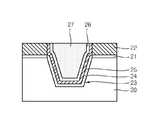
도 2a 내지 도 2d는 본 발명에 따른 반도체소자의 소자분리막 형성방법을 설명하기 위한 공정단면도이다.2A through 2D are cross-sectional views illustrating a method of forming a device isolation film of a semiconductor device according to the present invention.
본 발명에 따른 반도체소자의 소자분리막 형성방법은, 도 2a에 도시된 바와 같이, 소자분리예정영역이 정의된 실리콘기판(20)을 제공한다. 이어, 상기 실리콘 기판(20)상에 100Å 두께의 패드산화막(21)과 1,400Å 두께의 패드질화막(22)을 차례로 형성한 다음, 상기 패드질화막(22) 위에 감광막을 도포하고 노광 및 현상하여 소자분리예정영역을 노출시키는 감광막 패턴(30)을 형성한다.The method of forming a device isolation film of a semiconductor device according to the present invention provides a
그런 다음, 도 2b에 도시된 바와 같이, 상기 감광막 패턴을 마스크로 하여 소자분리 영역에 해당하는 기판 부분을 노출시키도록 상기 패드질화막(22)과 패드산화막(21)을 공지의 리소그라피 공정으로 패터닝한다. 이어서, 감광막 패턴을 제거하고 나서, 상기 잔류된 패드질화막을 마스크로 하여 노출된 실리콘 기판 부분을 소정 깊이 만큼 식각하여 트렌치(23)를 형성한다.Then, as shown in FIG. 2B, the
이후, 상기 트렌치(23) 식각시 유발되는 스트레스를 제거하고, 반도체 기판(20)을 보호하기 위해, 트렌치(23)가 형성된 반도체 기판(20)상에 희생산화막(미도시) 형성 및 제거한다. 이어서 사이드 월 산화(side wall oxidation) 공정을 수행하여 박막의 산화막(24)을 형성한다.Thereafter, in order to remove the stress caused when the
이 후, 상기 박막의 산화막(24)이 형성된 전체구조 상면에 소정의 질화막(25) 및 산화막(26)을 차례로 형성한다. 이 때, 상기 질화막(25)은 질화막과 이후 형성될 소자분리막과의 식각량 차이에 의해 호(moat) 예컨대, 실리콘 액티브 영역과 소자분리막이 만나는 곳에 푹 파인 곳의 깊이를 줄이는 역할을 하게 된다. 또한, 상기 산화막(26)은 질화막(25)의 손실(loss)을 방지하기 위한 역할을 하게 된다.Thereafter, a
이어, 상기 산화막(26)을 포함한 트렌치 구조 전면에 화학기상증착 방법으로 갭필산화막(27)을 형성한다. 이때, 상기 갭필산화막(27)으로는 기존의 HDP산화막 대신 Al2O3막을 이용한다. 상기 Al2O3막은 300∼500℃의 온도 및 0.1∼ 5토르의 압력 하에서, 소오스로서 TMA 및 TEA 중 어느 하나를 이용하여 증착방법으로 형성한다. 또한, 상기 증착공정은 싱글타입(ingle type) 또는 배치타입(batch type) 중 어느 하나의 장비내에서 진행한다.Subsequently, a gap
한편, 상기 Al2O3막은 이후의 습식식각 공정에서 손실됨이 없도록 하기 위해, 50:1 비율의 HF 케미컬에서 습식식각비가 적어도 0.5Å/sec 이하이어야 한다.On the other hand, in order to prevent the Al2O3 film from being lost in a subsequent wet etching process, a wet etching ratio of HF chemical in a 50: 1 ratio should be at least 0.5 μs / sec or less.
그런 다음, 도 2c에 도시된 바와 같이, 상기 패드질화막(22)이 노출되도록 갭필산화막(27)인 Al2O3막, 산화막(26) 및 질화막(25)을 화학적기계연마(Chemical Mechanical Polishing : 이하, CMP) 공정으로 연마한다.Then, as illustrated in FIG. 2C, the Al 2 O 3 film, the
이어서, 도 2d에 도시된 바와 같이, 패드질화막을 인산용액을 이용한 습식 식각 공정을 통해 제거하고 나서, 상기 결과물을 불산용액에 디핑처리시켜 패드산화막을 제거하고, 이 결과로, 트렌치형의 소자분리막(28)을 형성한다. 이때, 상기 Al2O3막 재질의 소자분리막은 인산, 불산 등의 케미컬을 이용한 습식식각 공정을 진행하여도 식각되지 않음을 알 수 있다.Subsequently, as shown in FIG. 2D, the pad nitride film is removed through a wet etching process using a phosphoric acid solution, and then the resultant is dipped in a hydrofluoric acid solution to remove the pad oxide film. As a result, a trench type device isolation film is obtained.
그런 다음, 상기 소자분리막(28)을 포함한 기판 전면에 게이트산화막(29) 및 게이트 형성용 다결정실리콘막(30)을 차례로 증착한다.Thereafter, a
이상에서와 같이, 본 발명은 소자격리를 위한 트렌치를 매립시키는 갭필산화막으로 습식식각비가 낮은 Al2O3막을 적용함으로써, 후속의 습식식각 공정에 의한 산화막 손실을 최소화하며, 이로써 소자분리막의 높이 및 소자영역 크기를 일정수준으로 제어할 수 있다.As described above, the present invention minimizes the oxide loss by the subsequent wet etching process by applying an Al2O3 film having a low wet etching ratio as a gap fill oxide filling a trench for device isolation, thereby reducing the height of the device isolation layer and the device region size. Can be controlled to a certain level.
따라서, 본 발명은 소자 특성치의 예상이 용이하여 생산수율 증대와 안정성을 확보할 수 있다. Therefore, the present invention can easily predict the device characteristic value, it is possible to ensure the production yield increase and stability.
기타, 본 발명은 그 요지를 일탈하지 않는 범위에서 다양하게 변경하여 실시할 수 있다.In addition, this invention can be implemented in various changes within the range which does not deviate from the summary.
Claims (5)
Translated fromKoreanPriority Applications (2)
| Application Number | Priority Date | Filing Date | Title |
|---|---|---|---|
| KR1020030084920AKR100548571B1 (en) | 2003-11-27 | 2003-11-27 | Method of forming device isolation film of semiconductor device |
| US10/889,480US7067390B2 (en) | 2003-11-27 | 2004-07-12 | Method for forming isolation layer of semiconductor device |
Applications Claiming Priority (1)
| Application Number | Priority Date | Filing Date | Title |
|---|---|---|---|
| KR1020030084920AKR100548571B1 (en) | 2003-11-27 | 2003-11-27 | Method of forming device isolation film of semiconductor device |
Publications (2)
| Publication Number | Publication Date |
|---|---|
| KR20050051175A KR20050051175A (en) | 2005-06-01 |
| KR100548571B1true KR100548571B1 (en) | 2006-02-02 |
Family
ID=34617299
Family Applications (1)
| Application Number | Title | Priority Date | Filing Date |
|---|---|---|---|
| KR1020030084920AExpired - Fee RelatedKR100548571B1 (en) | 2003-11-27 | 2003-11-27 | Method of forming device isolation film of semiconductor device |
Country Status (2)
| Country | Link |
|---|---|
| US (1) | US7067390B2 (en) |
| KR (1) | KR100548571B1 (en) |
Families Citing this family (2)
| Publication number | Priority date | Publication date | Assignee | Title |
|---|---|---|---|---|
| CN115662903B (en)* | 2022-11-14 | 2023-05-26 | 合肥晶合集成电路股份有限公司 | Method for manufacturing semiconductor device and semiconductor device |
| CN119108337A (en)* | 2024-09-05 | 2024-12-10 | 浙江创芯集成电路有限公司 | Method for forming semiconductor structure |
Family Cites Families (3)
| Publication number | Priority date | Publication date | Assignee | Title |
|---|---|---|---|---|
| US6653200B2 (en)* | 2001-01-26 | 2003-11-25 | Applied Materials, Inc. | Trench fill process for reducing stress in shallow trench isolation |
| KR100428804B1 (en)* | 2001-02-23 | 2004-04-29 | 삼성전자주식회사 | Method of forming a layer in an integrated circuit device process, a method for fabricating a trench isolaton using the same and a trench isolation structure |
| US6861334B2 (en)* | 2001-06-21 | 2005-03-01 | Asm International, N.V. | Method of fabricating trench isolation structures for integrated circuits using atomic layer deposition |
- 2003
- 2003-11-27KRKR1020030084920Apatent/KR100548571B1/ennot_activeExpired - Fee Related
- 2004
- 2004-07-12USUS10/889,480patent/US7067390B2/ennot_activeExpired - Fee Related
Also Published As
| Publication number | Publication date |
|---|---|
| US20050118786A1 (en) | 2005-06-02 |
| KR20050051175A (en) | 2005-06-01 |
| US7067390B2 (en) | 2006-06-27 |
Similar Documents
| Publication | Publication Date | Title |
|---|---|---|
| KR100224700B1 (en) | Isolation method of semiconductor device | |
| US7067387B2 (en) | Method of manufacturing dielectric isolated silicon structure | |
| US6103581A (en) | Method for producing shallow trench isolation structure | |
| KR100548571B1 (en) | Method of forming device isolation film of semiconductor device | |
| KR20010046153A (en) | Method of manufacturing trench type isolation layer in semiconductor device | |
| KR100417853B1 (en) | Method for manufacturing device having a shallow trench isolation and deep trench isolation | |
| KR20030052663A (en) | method for isolating semiconductor device | |
| KR100528797B1 (en) | Method of forming an isolation film in a semiconductor device | |
| KR100561974B1 (en) | Manufacturing method of semiconductor device | |
| KR100587084B1 (en) | Manufacturing method of semiconductor device | |
| KR100954418B1 (en) | Device Separating Method of Semiconductor Device | |
| KR100486875B1 (en) | Isolation layer in a semiconductor device and a method of forming the same | |
| KR100800106B1 (en) | Trench insulating film formation method of a semiconductor device | |
| KR20070057576A (en) | Deformation Method of Deformed Shallow Trench Isolation of Semiconductor Devices | |
| KR20020001353A (en) | manufacturing method of semiconductor device with shallow trench | |
| KR20050051176A (en) | Method for forming isolation layer | |
| KR100541707B1 (en) | Device Separating Method of Semiconductor Device | |
| KR20050012652A (en) | Method for forming element isolation layer of semiconductor device | |
| KR20040105980A (en) | The method for forming shallow trench isolation in semiconductor device | |
| KR20040003649A (en) | Method for planation in semiconductor device | |
| KR20090037263A (en) | Device Separation Film of Semiconductor Device and Formation Method Thereof | |
| KR20030083448A (en) | Method for forming isolation layer of semiconductor device | |
| KR20050003046A (en) | Method of manufacturing isolation using liner nitride | |
| KR20050003013A (en) | Fabricating method forming isolation layer in semiconductor device | |
| KR20050059703A (en) | Method for forming isolation layer of semiconductor device |
Legal Events
| Date | Code | Title | Description |
|---|---|---|---|
| A201 | Request for examination | ||
| PA0109 | Patent application | St.27 status event code:A-0-1-A10-A12-nap-PA0109 | |
| PA0201 | Request for examination | St.27 status event code:A-1-2-D10-D11-exm-PA0201 | |
| PG1501 | Laying open of application | St.27 status event code:A-1-1-Q10-Q12-nap-PG1501 | |
| E902 | Notification of reason for refusal | ||
| PE0902 | Notice of grounds for rejection | St.27 status event code:A-1-2-D10-D21-exm-PE0902 | |
| E13-X000 | Pre-grant limitation requested | St.27 status event code:A-2-3-E10-E13-lim-X000 | |
| P11-X000 | Amendment of application requested | St.27 status event code:A-2-2-P10-P11-nap-X000 | |
| P13-X000 | Application amended | St.27 status event code:A-2-2-P10-P13-nap-X000 | |
| E701 | Decision to grant or registration of patent right | ||
| PE0701 | Decision of registration | St.27 status event code:A-1-2-D10-D22-exm-PE0701 | |
| GRNT | Written decision to grant | ||
| PR0701 | Registration of establishment | St.27 status event code:A-2-4-F10-F11-exm-PR0701 | |
| PR1002 | Payment of registration fee | St.27 status event code:A-2-2-U10-U11-oth-PR1002 Fee payment year number:1 | |
| PG1601 | Publication of registration | St.27 status event code:A-4-4-Q10-Q13-nap-PG1601 | |
| PR1001 | Payment of annual fee | St.27 status event code:A-4-4-U10-U11-oth-PR1001 Fee payment year number:4 | |
| PR1001 | Payment of annual fee | St.27 status event code:A-4-4-U10-U11-oth-PR1001 Fee payment year number:5 | |
| PR1001 | Payment of annual fee | St.27 status event code:A-4-4-U10-U11-oth-PR1001 Fee payment year number:6 | |
| PR1001 | Payment of annual fee | St.27 status event code:A-4-4-U10-U11-oth-PR1001 Fee payment year number:7 | |
| PN2301 | Change of applicant | St.27 status event code:A-5-5-R10-R13-asn-PN2301 St.27 status event code:A-5-5-R10-R11-asn-PN2301 | |
| FPAY | Annual fee payment | Payment date:20121224 Year of fee payment:8 | |
| PN2301 | Change of applicant | St.27 status event code:A-5-5-R10-R13-asn-PN2301 St.27 status event code:A-5-5-R10-R11-asn-PN2301 | |
| PR1001 | Payment of annual fee | St.27 status event code:A-4-4-U10-U11-oth-PR1001 Fee payment year number:8 | |
| FPAY | Annual fee payment | Payment date:20131231 Year of fee payment:9 | |
| PR1001 | Payment of annual fee | St.27 status event code:A-4-4-U10-U11-oth-PR1001 Fee payment year number:9 | |
| PN2301 | Change of applicant | St.27 status event code:A-5-5-R10-R11-asn-PN2301 | |
| PN2301 | Change of applicant | St.27 status event code:A-5-5-R10-R14-asn-PN2301 | |
| LAPS | Lapse due to unpaid annual fee | ||
| PC1903 | Unpaid annual fee | St.27 status event code:A-4-4-U10-U13-oth-PC1903 Not in force date:20150125 Payment event data comment text:Termination Category : DEFAULT_OF_REGISTRATION_FEE | |
| PN2301 | Change of applicant | St.27 status event code:A-5-5-R10-R13-asn-PN2301 St.27 status event code:A-5-5-R10-R11-asn-PN2301 | |
| PC1903 | Unpaid annual fee | St.27 status event code:N-4-6-H10-H13-oth-PC1903 Ip right cessation event data comment text:Termination Category : DEFAULT_OF_REGISTRATION_FEE Not in force date:20150125 |