KR100547059B1 - Semiconductor device and manufacturing method thereof - Google Patents
Semiconductor device and manufacturing method thereofDownload PDFInfo
- Publication number
- KR100547059B1 KR100547059B1KR1020020058411AKR20020058411AKR100547059B1KR 100547059 B1KR100547059 B1KR 100547059B1KR 1020020058411 AKR1020020058411 AKR 1020020058411AKR 20020058411 AKR20020058411 AKR 20020058411AKR 100547059 B1KR100547059 B1KR 100547059B1
- Authority
- KR
- South Korea
- Prior art keywords
- region
- bulk
- soi
- layer
- boundary
- Prior art date
- Legal status (The legal status is an assumption and is not a legal conclusion. Google has not performed a legal analysis and makes no representation as to the accuracy of the status listed.)
- Expired - Fee Related
Links
Images


Classifications
- H—ELECTRICITY
- H10—SEMICONDUCTOR DEVICES; ELECTRIC SOLID-STATE DEVICES NOT OTHERWISE PROVIDED FOR
- H10D—INORGANIC ELECTRIC SEMICONDUCTOR DEVICES
- H10D86/00—Integrated devices formed in or on insulating or conducting substrates, e.g. formed in silicon-on-insulator [SOI] substrates or on stainless steel or glass substrates
- H—ELECTRICITY
- H01—ELECTRIC ELEMENTS
- H01L—SEMICONDUCTOR DEVICES NOT COVERED BY CLASS H10
- H01L21/00—Processes or apparatus adapted for the manufacture or treatment of semiconductor or solid state devices or of parts thereof
- H01L21/70—Manufacture or treatment of devices consisting of a plurality of solid state components formed in or on a common substrate or of parts thereof; Manufacture of integrated circuit devices or of parts thereof
- H01L21/71—Manufacture of specific parts of devices defined in group H01L21/70
- H01L21/76—Making of isolation regions between components
- H01L21/762—Dielectric regions, e.g. EPIC dielectric isolation, LOCOS; Trench refilling techniques, SOI technology, use of channel stoppers
- H01L21/7624—Dielectric regions, e.g. EPIC dielectric isolation, LOCOS; Trench refilling techniques, SOI technology, use of channel stoppers using semiconductor on insulator [SOI] technology
- H01L21/76264—SOI together with lateral isolation, e.g. using local oxidation of silicon, or dielectric or polycristalline material refilled trench or air gap isolation regions, e.g. completely isolated semiconductor islands
- H—ELECTRICITY
- H10—SEMICONDUCTOR DEVICES; ELECTRIC SOLID-STATE DEVICES NOT OTHERWISE PROVIDED FOR
- H10B—ELECTRONIC MEMORY DEVICES
- H10B12/00—Dynamic random access memory [DRAM] devices
- H10B12/01—Manufacture or treatment
- H10B12/09—Manufacture or treatment with simultaneous manufacture of the peripheral circuit region and memory cells
- H—ELECTRICITY
- H10—SEMICONDUCTOR DEVICES; ELECTRIC SOLID-STATE DEVICES NOT OTHERWISE PROVIDED FOR
- H10D—INORGANIC ELECTRIC SEMICONDUCTOR DEVICES
- H10D86/00—Integrated devices formed in or on insulating or conducting substrates, e.g. formed in silicon-on-insulator [SOI] substrates or on stainless steel or glass substrates
- H10D86/01—Manufacture or treatment
- H—ELECTRICITY
- H10—SEMICONDUCTOR DEVICES; ELECTRIC SOLID-STATE DEVICES NOT OTHERWISE PROVIDED FOR
- H10D—INORGANIC ELECTRIC SEMICONDUCTOR DEVICES
- H10D86/00—Integrated devices formed in or on insulating or conducting substrates, e.g. formed in silicon-on-insulator [SOI] substrates or on stainless steel or glass substrates
- H10D86/201—Integrated devices formed in or on insulating or conducting substrates, e.g. formed in silicon-on-insulator [SOI] substrates or on stainless steel or glass substrates the substrates comprising an insulating layer on a semiconductor body, e.g. SOI
- H—ELECTRICITY
- H10—SEMICONDUCTOR DEVICES; ELECTRIC SOLID-STATE DEVICES NOT OTHERWISE PROVIDED FOR
- H10D—INORGANIC ELECTRIC SEMICONDUCTOR DEVICES
- H10D87/00—Integrated devices comprising both bulk components and either SOI or SOS components on the same substrate
- H—ELECTRICITY
- H01—ELECTRIC ELEMENTS
- H01L—SEMICONDUCTOR DEVICES NOT COVERED BY CLASS H10
- H01L21/00—Processes or apparatus adapted for the manufacture or treatment of semiconductor or solid state devices or of parts thereof
- H01L21/70—Manufacture or treatment of devices consisting of a plurality of solid state components formed in or on a common substrate or of parts thereof; Manufacture of integrated circuit devices or of parts thereof
- H01L21/71—Manufacture of specific parts of devices defined in group H01L21/70
- H01L21/76—Making of isolation regions between components
- H01L21/762—Dielectric regions, e.g. EPIC dielectric isolation, LOCOS; Trench refilling techniques, SOI technology, use of channel stoppers
- H01L21/7624—Dielectric regions, e.g. EPIC dielectric isolation, LOCOS; Trench refilling techniques, SOI technology, use of channel stoppers using semiconductor on insulator [SOI] technology
- H01L21/76264—SOI together with lateral isolation, e.g. using local oxidation of silicon, or dielectric or polycristalline material refilled trench or air gap isolation regions, e.g. completely isolated semiconductor islands
- H01L21/76283—Lateral isolation by refilling of trenches with dielectric material
- H—ELECTRICITY
- H01—ELECTRIC ELEMENTS
- H01L—SEMICONDUCTOR DEVICES NOT COVERED BY CLASS H10
- H01L2924/00—Indexing scheme for arrangements or methods for connecting or disconnecting semiconductor or solid-state bodies as covered by H01L24/00
- H01L2924/0001—Technical content checked by a classifier
- H01L2924/0002—Not covered by any one of groups H01L24/00, H01L24/00 and H01L2224/00
- H—ELECTRICITY
- H10—SEMICONDUCTOR DEVICES; ELECTRIC SOLID-STATE DEVICES NOT OTHERWISE PROVIDED FOR
- H10B—ELECTRONIC MEMORY DEVICES
- H10B12/00—Dynamic random access memory [DRAM] devices
- H10B12/01—Manufacture or treatment
- H10B12/02—Manufacture or treatment for one transistor one-capacitor [1T-1C] memory cells
- H10B12/03—Making the capacitor or connections thereto
- H10B12/038—Making the capacitor or connections thereto the capacitor being in a trench in the substrate
- H—ELECTRICITY
- H10—SEMICONDUCTOR DEVICES; ELECTRIC SOLID-STATE DEVICES NOT OTHERWISE PROVIDED FOR
- H10B—ELECTRONIC MEMORY DEVICES
- H10B12/00—Dynamic random access memory [DRAM] devices
- H10B12/30—DRAM devices comprising one-transistor - one-capacitor [1T-1C] memory cells
- H10B12/37—DRAM devices comprising one-transistor - one-capacitor [1T-1C] memory cells the capacitor being at least partially in a trench in the substrate
- H10B12/373—DRAM devices comprising one-transistor - one-capacitor [1T-1C] memory cells the capacitor being at least partially in a trench in the substrate the capacitor extending under or around the transistor
Landscapes
- Engineering & Computer Science (AREA)
- Manufacturing & Machinery (AREA)
- Physics & Mathematics (AREA)
- Condensed Matter Physics & Semiconductors (AREA)
- General Physics & Mathematics (AREA)
- Computer Hardware Design (AREA)
- Microelectronics & Electronic Packaging (AREA)
- Power Engineering (AREA)
- Semiconductor Memories (AREA)
- Element Separation (AREA)
- Metal-Oxide And Bipolar Metal-Oxide Semiconductor Integrated Circuits (AREA)
Abstract
Translated fromKoreanDescription
Translated fromKorean도 1은 본 발명이 적용되는 반도체 칩의 평면 구성예를 도시하는 도면.BRIEF DESCRIPTION OF THE DRAWINGS The figure which shows the example of planar structure of the semiconductor chip to which this invention is applied.
도 2는 제1 실시예에 따른 반도체 장치의 개략 단면도.2 is a schematic cross-sectional view of a semiconductor device according to the first embodiment.
도 3a∼도 3g는 도 2에 도시한 반도체 장치의 제조 공정을 도시하는 도면.3A to 3G are diagrams illustrating a manufacturing process of the semiconductor device shown in FIG. 2.
도 4는 제2 실시예에 따른 반도체 장치의 개략 단면도.4 is a schematic cross-sectional view of a semiconductor device according to the second embodiment.
도 5a∼도 5c는 도 4에 도시한 반도체 장치의 제조 공정을 도시하는 도면.5A to 5C are diagrams showing manufacturing steps of the semiconductor device shown in FIG. 4.
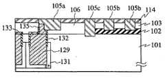
도 6은 제3 실시예에 따른 반도체 장치의 개략 단면도.6 is a schematic cross-sectional view of a semiconductor device according to the third embodiment.
도 7a∼도 7f는 도 6에 도시한 반도체 장치의 제조 공정을 도시하는 도면.7A to 7F are diagrams illustrating a manufacturing process of the semiconductor device shown in FIG. 6.
도 8a∼도 8c는 도 6에 도시한 반도체 장치의 다른 제조 공정을 나타내고, 도 8c 이후의 공정은, 도 7d∼도 7f와 마찬가지이다.8A to 8C show another manufacturing process of the semiconductor device shown in FIG. 6, and the processes subsequent to FIG. 8C are the same as those of FIGS. 7D to 7F.
도 9a 및 도 9b는 제4 실시예에 따른 반도체 장치의 개략 단면도.9A and 9B are schematic cross-sectional views of a semiconductor device according to the fourth embodiment.
도 10은 제5 실시예에 따른 반도체 장치의 개략 단면도.10 is a schematic cross-sectional view of a semiconductor device according to the fifth embodiment.
도 11a∼도 11g는 도 10에 도시한 반도체 장치의 제조 공정을 도시하는 도면.11A to 11G are diagrams illustrating a manufacturing process of the semiconductor device shown in FIG. 10.
도 12는 도 10에 도시한 반도체 장치의 변형예를 도시하는 도면.FIG. 12 is a diagram showing a modification of the semiconductor device shown in FIG. 10.
도 13은 제6 실시예에 따른 반도체 장치의 개략 단면도.13 is a schematic cross-sectional view of a semiconductor device according to the sixth embodiment.
도 14는 도 13에 도시한 반도체 장치에서 이용되는 더미 캐패시터의 배치예를 도시하는 도면.FIG. 14 is a diagram showing an arrangement example of dummy capacitors used in the semiconductor device shown in FIG. 13; FIG.
도 15는 도 13에 도시한 반도체 장치에서 이용되는 더미 패턴의 변형예를 도시하는 도면.FIG. 15 is a diagram showing a modification of the dummy pattern used in the semiconductor device shown in FIG. 13.
<도면의 주요 부분에 대한 부호의 설명><Explanation of symbols for main parts of the drawings>
10 : 반도체 칩10: semiconductor chip
11 : 벌크 소자 영역11: bulk device region
12 : SOI 소자 영역12: SOI device area
20 : SOI 웨이퍼20: SOI wafer
21 : Si 지지 기판21: Si support substrate
22 : 매립 절연막22: buried insulation film
22' : 매립 산화막22 ': buried oxide film
23 : SOI층23: SOI layer
24 : 마스크 패턴24: mask pattern
25 : 측벽 보호막25: sidewall protective film
26 : 벌크 성장층26: bulk growth layer
27 : 마스크재27: mask material
29 : 축적 전극29: accumulation electrode
30 : 트렌치 캐패시터30: trench capacitor
31 : 하부 확산 플레이트31: lower diffusion plate
32 : 컬러 절연막32: color insulating film
33 : 스트랩33: strap
35a, 35b : 소자 분리 영역35a, 35b: device isolation region
40a : n형 소스/드레인 확산층40a: n-type source / drain diffusion layer
43 : DRAM셀43: DRAM cell
44 : 주변 트랜지스터44: peripheral transistor
45 : MOSFET45 MOSFET
본 발명은, 반도체 장치와 그 제조 방법에 관한 것으로, 특히 SOI(silicon-on-insulator) 기판 영역에 형성되는 회로 소자와, 벌크(Bulk) 기판 영역에 형성되는 회로 소자를 동일 칩 상에 탑재한 반도체 장치, 및 그 제조 방법에 관한 것이다.BACKGROUND OF THE
하나의 MOSFET와 하나의 캐패시터로 구성되는 1T1C(1 트랜지스터 1 캐패시터)형 메모리 셀을 갖는 DRAM은, 고집적화에 적합한 염가인 대용량 메모리로서, 광범위한 용도에 이용되고 있다. 특히, 최근 이러한 DRAM과 로직 회로를 동일한 반도체 칩 상에 집적하여, 시스템 성능을 향상하는 시스템 LSI로의 요구가 높아지고 있다.A DRAM having a 1T1C (1
한편, MOSFET를 중심으로 구성하는 로직 회로의 고성능화를 도모하기 위하 여, 종래의 실리콘 벌크 기판을 대신하여, SOI 기판의 표면측 박막 실리콘층(이하, 「SOI층」이라고 칭함)에 트랜지스터를 형성한 SOIMOSFET 등의 SOI 소자가 각광을 받아, 이미 고성능 로직 용도로 제품화가 시작되고 있다. 이러한 흐름 중에서, SOI 소자로 구성되는 고성능 로직 회로(이하, 「SOI 로직」이라고 칭함)의 성능을 더 이끌어내도록, DRAM 등의 메모리를 SOI 로직과 함께 탑재한 시스템 LSI 혹은 시스템 온 칩의 개발이 급선무이다.On the other hand, in order to improve the performance of logic circuits mainly composed of MOSFETs, transistors are formed on the surface-side thin film silicon layer (hereinafter referred to as "SOI layer") of the SOI substrate in place of the conventional silicon bulk substrate. SOI devices such as SOIMOSFETs are in the spotlight, and commercialization has already begun for high performance logic. In such a flow, development of a system LSI or a system on a chip having a memory such as DRAM together with the SOI logic is urgently required to further derive the performance of a high-performance logic circuit composed of SOI elements (hereinafter referred to as "SOI logic"). to be.
그러나, SOI 기판 상에 고성능 로직을 구성하는 소자(예를 들면, SOIM OSFET)와 동일한 구조로 DRAM을 형성하는 것은, 이하의 이유로 곤란하다.However, it is difficult to form DRAM on the SOI substrate with the same structure as an element (for example, SOIM OSFET) constituting high performance logic for the following reasons.
우선, SOIMOSFET는, 일반적인 사용에 있어서, 채널이 형성되는 보디 영역의 전위가 부유가 되기 때문에, 회로 동작에 수반하는 누설 전류나 임계치 변동을 일으킨다. 예를 들면, 패스 트랜지스터로서 이용한 경우, 게이트 전압이 오프가 되는 조건 하에 있더라도, 소스·드레인 전압의 동작 조건에 의해서는, 기생 MOSFET 전류나 기생 바이폴라 전류라고 하는 누설 전류가 흐르는 경우가 있다. 이 때문에, 보유의 문제에서 볼 때, DRAM의 셀 트랜지스터와 같이 누설 전류 스펙이 엄격한 회로에 SOIMOSFET를 적용하는 것은 부적합하다.First, in the general use of SOIMOSFET, since the potential of the body region in which the channel is formed becomes floating, the SOIMOSFET causes leakage current and threshold variation accompanying the circuit operation. For example, when used as a pass transistor, even when the gate voltage is turned off, a leakage current such as a parasitic MOSFET current or a parasitic bipolar current may flow under operating conditions of the source and drain voltages. For this reason, in view of the retention problem, it is inappropriate to apply the SOIMOSFET to a circuit with a tight leakage current specification such as a DRAM cell transistor.
또한, 기판 부유 효과에 의해, 트랜지스터의 동작 이력을 포함하는 동작 조건의 차이에 따라 임계 전압에 변동이 생긴다. 이 때문에, SOIMOSFET를 DRAM의 감지 증폭기 회로에 이용하는 경우, 트랜지스터 쌍 간의 임계 전압의 변동을 증폭하여, 감지 마진을 열화시키기 위해서 부적합하다.In addition, the substrate floating effect causes variation in the threshold voltage depending on the difference in operating conditions including the operation history of the transistor. For this reason, when the SOIMOSFET is used in the sense amplifier circuit of a DRAM, it is unsuitable for amplifying the variation of the threshold voltage between the transistor pairs and degrading the sense margin.
이러한 기판 부유 효과에 의한 문제점을 해결하는 방법으로서, 종래의 MOSFET 패턴에 대하여 보디부에서 인출하여 소자 영역과 컨택트를 형성하여 보디 전위를 고정하는 방법도 제안되어 있다. 그러나, 이 방법으로는, 셀이나 감지 증폭기부의 면적이 대폭 증대하여, DRAM의 최대의 특장인 고집적성을 손상시킨다는 문제가 있다.As a method of solving such a problem caused by the substrate floating effect, a method of fixing the body potential by drawing a contact from the body portion and forming a contact with the element region with respect to the conventional MOSFET pattern has also been proposed. However, this method has a problem in that the area of the cell and the sense amplifier section is greatly increased, thereby impairing high integration, which is the greatest feature of the DRAM.
그래서, SOI 기판에 일부 벌크 영역을 형성하고, 벌크 영역 내에, 기판 부유 효과와 특성이 맞지 않는 DRAM 등의 회로를 형성하는 것을 생각할 수 있다. 실제로, 이것을 실현하기 위해서, SOI 기판 중에 벌크 영역을 구비한 기판(이하 「SOI/벌크 기판」 이라 함)의 형성 방법이 여러가지 제안되어 있다.Therefore, it is conceivable to form a partial bulk region in the SOI substrate, and to form a circuit such as a DRAM in the bulk region that does not match the substrate floating effect. In practice, various methods for forming a substrate (hereinafter referred to as " SOI / bulk substrate ") having a bulk region in the SOI substrate have been proposed.
제1 방법으로서, 마스크 패턴을 이용한 SIMOX(Separation by Implanted Oxygen)법에 의해, Si 기판의 원하는 위치에 산소 주입을 행하여, SOI 기판 중에 벌크 영역을 형성하는 방법(일본 특개평 10-303385호 공보, 및 Robert Hannon, et al. 2000 Symposium on VLSI Technology of Technical Papers, pp66-67)이 있다.As a first method, a method of forming a bulk region in an SOI substrate by performing oxygen injection at a desired position of a Si substrate by a SIMOX (Separation by Implanted Oxygen) method using a mask pattern (Japanese Patent Laid-Open No. 10-303385, And Robert Hannon, et al. 2000 Symposium on VLSI Technology of Technical Papers, pp66-67.
제2 방법은, 절연막을 패터닝한 실리콘(Si) 기판 상에 다른 실리콘(Si) 기판을 접합시킴으로써, SOI 영역과 벌크 영역을 혼재시키는 방법이다(일본 특개평 8-316431호 공보).The second method is a method in which an SOI region and a bulk region are mixed by bonding another silicon (Si) substrate onto a silicon (Si) substrate on which an insulating film is patterned (Japanese Patent Laid-Open No. 8-316431).
제3 방법은, SOI 기판의 소정의 위치에서 표면의 SOI층과, 그 하방의 매립 절연막을 부분적으로 에칭 제거하여 지지 기판을 노출하여, SOI 기판 내에 벌크 영역을 제작하는 방법(일본 특개평 7-106434호 공보, 일본 특개평 11-238860호 공보, 및 일본 특개 2000-91534호 공보)이다.The third method is a method of manufacturing a bulk region in an SOI substrate by partially etching away the surface SOI layer and the buried insulating film below it at a predetermined position of the SOI substrate to expose the supporting substrate (Japanese Patent Laid-Open No. 7-A). 106434, Japanese Patent Laid-Open No. 11-238860, and Japanese Patent Laid-Open No. 2000-91534.
제4 방법은, 제3 방법에 의한 부분 에칭 제거로 생긴 SOI 영역과 벌크 영역 의 단차를 해소하기 위해서, 벌크 영역에 Si 에피택셜 성장층을 형성하는 방법이다. 이 방법으로는, 에피택셜 성장층을 SOI 영역 상의 마스크재보다도 높은 위치까지 형성하고, 그 후 마스크재를 스토퍼로 하여 에피택셜 성장층을 연마하여 평탄화한다(일본 특개 2000-243944호 공보).The fourth method is a method of forming a Si epitaxially grown layer in the bulk region in order to eliminate the step difference between the SOI region and the bulk region caused by partial etching removal by the third method. In this method, the epitaxial growth layer is formed to a position higher than the mask material on the SOI region, and the epitaxial growth layer is then polished and planarized using the mask material as a stopper (Japanese Patent Laid-Open No. 2000-243944).
이들 SOI/벌크 기판 형성 방법은, 모두 이하의 문제점을 갖는다.These SOI / bulk substrate formation methods all have the following problems.
제1 방법에서는, 산소 이온 주입에 의한 손상에 의해, SOI층의 결정성이 좋지 않다. 또한, 산소 이온 주입에 의한 매립 산화막 형성 시에 체적 팽창에 의한 응력이 생겨서, SOI 영역과 벌크 영역의 경계부에 결정 결함이 발생한다.In the first method, the crystallinity of the SOI layer is poor due to damage caused by oxygen ion implantation. In addition, when the buried oxide film is formed by oxygen ion implantation, stress due to volume expansion occurs, and crystal defects occur at the boundary between the SOI region and the bulk region.
제2 방법에서는, Si 기판끼리의 접합면에서, 오염물이나 결정 방위의 어긋남 등에 의해 결정성의 열화나 전기적 특성의 열화로 이어지는 계면 단위나 결정 결함층의 형성이 발생한다. 이 때문에, 벌크 영역에서 필요하게 되는 웰 접합이나 트렌치 캐패시터 등의 깊은 소자에서 특성 열화를 유발한다.In the second method, formation of interfacial units or crystal defect layers that lead to deterioration of crystallinity and deterioration of electrical characteristics occurs due to contamination or shift of crystal orientation in the bonding surface between Si substrates. This causes property deterioration in deep devices such as well junctions and trench capacitors that are needed in the bulk region.
제3 방법에서는, SOI 영역과 벌크 영역 사이에 SOI층과 매립 절연막의 두께 분에 상당하는 단차가 발생하여, 리소그래피 공정의 포커스 마진의 확보나 소자 분리 영역 형성 시의 절연막의 매립 높이의 제어가 곤란하게 된다.In the third method, a step corresponding to the thickness of the SOI layer and the buried insulating film is generated between the SOI region and the bulk region, making it difficult to secure the focus margin in the lithography process or to control the buried height of the insulating film at the time of forming the element isolation region. Done.
제4 방법에서는, 벌크 영역을 구성하는 에피택셜 성장층의 측면이 SOI 기판과의 경계와 접하는 부분에서 결정이 열화한다는 문제가 있다. 이것은 노출된 SOI층 측면으로부터도 에피택셜층이 성장하는 것에 기인한다. 에칭면인 SOI층 측벽으로부터의 에피택셜층은 원래 결정성이 나쁜 데다가, 인접하는 지지 기판으로부터 성장한 결정과 접촉하는 영역에서 결정 방위의 미스매치가 생겨 결정성이 더 악화하기 때문이다.In the fourth method, there is a problem that crystals deteriorate at the portion where the side surface of the epitaxial growth layer constituting the bulk region is in contact with the boundary with the SOI substrate. This is due to the growth of the epitaxial layer also from the exposed SOI layer side. This is because the epitaxial layer from the SOI layer sidewall, which is the etching surface, is originally poor in crystallinity, and mismatches in crystal orientation occur in regions in contact with crystals grown from adjacent support substrates, thereby deteriorating crystallinity.
또한, 단차 해소를 위해 형성한 에피택셜 성장층의 표면을 연마 평탄화한다 고 해도, 사전에 SOI층 상에 형성한 마스크재를 스토퍼로 하여 연마한다. 이와 같이 하면 에피택셜 성장층 표면의 높이가 마스크재의 두께 만큼 SOI층 표면의 높이보다도 높아지기 때문에, 연마 후에 마스크재를 더 얇게 하여, 재차 연마하는 등, 번잡하고 마진이 좁은 후처리를 행하지 않으면 안된다. 또한, DRAM 매크로를 형성하는 경우 등, 성장층 영역이 넓은 경우에는, 연마에 의해 중앙 부분이 우묵하게 들어가는 디싱이 생긴다. 이러한 표면 위치의 불균형은, 후공정에서 단차로서 남아, 제조 공정에 악영향을 미친다.Further, even if the surface of the epitaxially grown layer formed for step difference elimination is polished and planarized, the mask material formed on the SOI layer in advance is polished as a stopper. In this case, since the height of the surface of the epitaxially grown layer is higher than the height of the surface of the SOI layer by the thickness of the mask material, complicated and narrow marginal post-treatment, such as thinning the mask material and polishing again, must be performed. In addition, when the growth layer region is large, such as when a DRAM macro is formed, dishing occurs in which the center portion is recessed by polishing. This surface position imbalance remains as a step in a later step, adversely affecting the manufacturing step.
그래서, 이들의 문제점을 해결하는 새로운 방법이 기대된다.Thus, new ways of solving these problems are expected.
본 발명의 제1 양상으로서, 반도체 장치는, 지지 기판과, 지지 기판 상에 형성된 벌크 성장층에 소자가 형성되는 벌크 소자 영역과, 지지 기판 상에 매립 절연막 및 매립 절연막 상의 SOI층을 갖고 상기 SOI층에 소자가 형성되는 SOI 소자 영역과, 이들 벌크 소자 영역과 SOI 소자 영역의 경계에 위치하는 경계층을 갖는다. 벌크 소자 영역에 소자가 형성되는 제1 소자 형성면과 SOI 소자 영역 내에 소자가 형성되는 제2 소자 형성면은 거의 동일한 높이에 위치한다.According to a first aspect of the present invention, a semiconductor device includes a support substrate, a bulk element region in which elements are formed in a bulk growth layer formed on the support substrate, and a buried insulating film and an SOI layer on the buried insulating film on the support substrate. An SOI element region in which elements are formed in the layer, and a boundary layer positioned at the boundary between these bulk element regions and the SOI element region. The first element formation surface on which the element is formed in the bulk element region and the second element formation surface on which the element is formed in the SOI element region are located at substantially the same height.
제2 양상으로서, 반도체 장치의 제조 방법은, (a) 지지 기판과, 지지 기판 상의 매립 절연막과, 매립 절연막 상의 실리콘층으로 구성되는 SOI 기판을 준비하고, (b) SOI 기판의 소정의 위치에서 상기 실리콘층과 매립 절연막의 일부를 제거하고, (c) 제거에 의해 노출된 실리콘층의 측벽을 덮는 측벽 보호막을 형성하고, (d) 상기 소정의 위치에서 상기 지지 기판의 표면을 노출시키고, 노출된 면으로부터 상기 실리콘층의 표면에 일치하는 높이의 벌크 성장층을 형성하고, (e) 벌크 성장층과 상기 SOI 기판에, 동일한 깊이의 소자 분리 영역을 일괄하여 형성하고, (f) 벌크 성장층과 SOI 기판에 소자를 형성한다.As a second aspect, a method of manufacturing a semiconductor device includes (a) preparing an SOI substrate composed of a support substrate, a buried insulating film on the support substrate, and a silicon layer on the buried insulating film, and (b) at a predetermined position of the SOI substrate. A portion of the silicon layer and the buried insulating film is removed, and (c) a sidewall protective film is formed covering the sidewalls of the silicon layer exposed by removal; (d) the surface of the support substrate is exposed at the predetermined position and exposed; Forming a bulk growth layer having a height corresponding to the surface of the silicon layer from the surface, (e) forming a device isolation region of the same depth in a bulk growth layer and the SOI substrate, and (f) a bulk growth layer And an element on the SOI substrate.
제3 양상으로서, 반도체 장치의 다른 제조 방법은, (a) 지지 기판과, 지지 기판 상의 매립 절연막과, 매립 절연막 상의 실리콘층으로 구성되는 SOI 기판을 준비하고, (b) SOI 기판의 제1 위치에서 상기 실리콘층을 제거하고, 제거한 위치에 제1 소자 분리 영역을 형성하고, (c) 제1 소자 분리 영역으로 실리콘층의 측벽을 덮은 채로 제2 위치에서 지지 기판의 표면을 노출하고, (d) 노출된 지지 기판의 면에서 실리콘층의 표면에 일치하는 높이의 벌크 성장층을 형성하고, (e) 벌크 성장층에 제1 소자 분리 영역보다도 깊은 제2 소자 분리 영역을 형성하고, (f) 벌크 성장층과 실리콘층에 소자를 형성한다.As a third aspect, another method of manufacturing a semiconductor device includes (a) preparing an SOI substrate composed of a support substrate, a buried insulating film on the support substrate, and a silicon layer on the buried insulating film, and (b) a first position of the SOI substrate. Remove the silicon layer at and form a first device isolation region at the removed location, (c) expose the surface of the support substrate at a second location while covering the sidewall of the silicon layer with the first device isolation region, and (d A) a bulk growth layer having a height corresponding to the surface of the silicon layer on the exposed support substrate surface, (e) a second device isolation region deeper than the first device isolation region in the bulk growth layer, and (f) Devices are formed in the bulk growth layer and the silicon layer.
제4 양상으로서, 반도체 장치의 또 다른 제조 방법은, (a) 지지 기판, 지지 기판 상의 매립 절연막, 매립 절연막 상의 실리콘층으로 구성되는 SOI 기판을 준비하고, (b) SOI 기판의 소정의 위치에서 상기 실리콘층과 매립 절연막의 일부를 제거하여 지지 기판을 노출하고, (c) 노출된 지지 기판에 트렌치 캐패시터의 제1 폭을 갖는 제1 부분을 형성하고, (d) 지지 기판 표면에서 상기 실리콘층의 표면에 일치하는 높이의 벌크 성장층을 형성하고, (e) 벌크 성장층에 제1 폭보다 좁은 제2 폭을 갖고 제1 부분에 연결되는 트렌치 캐패시터의 제2 부분을 형성한다.As a fourth aspect, another method of manufacturing a semiconductor device includes (a) preparing an SOI substrate composed of a support substrate, a buried insulating film on the support substrate, and a silicon layer on the buried insulating film, and (b) at a predetermined position of the SOI substrate. A portion of the silicon layer and the buried insulating film are removed to expose the support substrate, (c) a first portion having a first width of the trench capacitor is formed in the exposed support substrate, and (d) the silicon layer on the support substrate surface. Forming a bulk growth layer of height corresponding to the surface of (e) and forming a second portion of the trench capacitor having a second width narrower than the first width and connected to the first portion in the bulk growth layer.
제5 양상으로서, 반도체 장치의 또 다른 제조 방법은, (a) 지지 기판과, 지지 기판 상의 매립 절연막과, 매립 절연막 상의 실리콘층으로 구성되는 SOI 기판을 준비하고, (b) SOI 기판의 소정의 위치에서 실리콘층과 매립 절연막을 제거하여 지지 기판의 표면을 노출하고, (c) 노출한 지지 기판의 표면에서 실리콘층의 표면에 일치하는 높이의 벌크 성장층을 형성하고, (d) 벌크 성장층의 경계 근방에 매립 절연막보다도 깊은 더미 패턴층을 형성하고, (e) 벌크 성장층과 SOI 기판의 소정의 위치에 소자를 형성한다.As a fifth aspect, another method of manufacturing a semiconductor device includes (a) preparing an SOI substrate composed of a support substrate, a buried insulating film on the support substrate, and a silicon layer on the buried insulating film, and (b) a predetermined method of the SOI substrate. Remove the silicon layer and the buried insulating film at the position to expose the surface of the support substrate, (c) form a bulk growth layer of height corresponding to the surface of the silicon layer on the exposed surface of the support substrate, and (d) the bulk growth layer A dummy pattern layer deeper than the buried insulating film is formed near the boundary of (e), and an element is formed at a predetermined position of the bulk growth layer and the SOI substrate.
<실시예><Example>
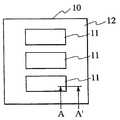
도 1은 본 발명이 적용되는 반도체 칩(10)의 평면 구성예를 나타낸다. 반도체 칩(10)은 벌크 기판 영역에 회로 소자가 형성되는 벌크 소자 영역(11)과, SOI 기판 영역에 소자가 형성되는 SOI 소자 영역(12)을 구비하고, 하나의 칩 상에 복수의 기능 회로를 탑재하고 시스템을 구성하는, 소위 시스템 온 칩형 반도체 장치이다.1 shows an example of a planar configuration of a
SOI 소자 영역(12)에서는, 매립 절연막 상의 박막 실리콘층(SOI층)에 소자가 형성된다. 이 영역에서는 소자 활성층의 바로 아래가 절연체가 되기 때문에, 로직 회로 등의 고속성, 고신뢰성을 필요로 하는 소자의 형성에 적합하다. 한편, 벌크 소자 영역(11)은 기판 부유 효과에 의한 문제를 피하기 위해서, SOI층 보다 벌크 기판에의 형성이 적합한 소자나 회로, 예를 들면 DRAM 셀이나 감지 증폭기 회로 등이 형성된다.In the
도 1a는 반도체 칩(10) 내에 단일의 벌크 소자 영역(11)을 배치한 예를, 도 1b는 반도체 칩(10) 내에 복수의 벌크 소자 영역(11)을 배치한 예를 나타낸다. 벌크 소자 영역(11)의 회로 소자로서 DRAM 셀을 형성하는 경우에는 벌크 소자 영역(11) 내에 DRAM 셀뿐만 아니라, 그 주변 회로(예를 들면, 감지 증폭기 회로, 전원 회로, 디코드 회로, I/O 회로, 혹은 이들의 조합 등)도 포함하여 형성되어, 전체로서의 하나의 기능 블록을 구성한다. 이러한 DRAM을 중심으로 하는 기능 블록을 「DRAM 매크로」라고 칭한다. 한편, SOI 소자 영역(12)에는 SOI층에, 예를 들면 MOS 트랜지스터를 형성한 고속 로직 회로가 형성된다. 이러한 로직 회로를 「SOI 로직」이라고 칭한다.FIG. 1A illustrates an example in which a single
도 1에 도시한 바와 같은 시스템 온 칩형 반도체 장치를 실현하기 위해서는, 하나의 기판 상에 부분적으로 SOI 기판 영역과, 벌크 기판 영역을 갖는, 소위 SOI/벌크 기판이 필요하다. 그러나, 종래의 SOI/벌크 기판 제작 방법에는 여러가지의 문제가 있는 것은 상술한 바와 같다.In order to realize a system-on-chip semiconductor device as shown in FIG. 1, a so-called SOI / bulk substrate having a SOI substrate region and a bulk substrate region partially on one substrate is required. However, as described above, there are various problems in the conventional SOI / bulk substrate fabrication method.
그래서, 종래 기술에서 진술한 제4 방법에서의 문제점, 즉 SOI 기판 영역과 벌크 기판 영역의 경계에서의 결정 열화를 방지하기 위해서, 에칭에 의해 노출된 SOI층의 측벽을 실리콘 질화막 등의 측벽 보호막으로 보호한 후에, 에피택셜 성장층을 형성하는 방법을 생각할 수 있다.Thus, in order to prevent problems in the fourth method stated in the prior art, that is, crystal deterioration at the boundary between the SOI substrate region and the bulk substrate region, sidewalls of the SOI layer exposed by etching are replaced with sidewall protective films such as silicon nitride films. After protection, the method of forming an epitaxial growth layer can be considered.
그러나, 에피택셜 성장에 의한 벌크 영역과 SOI 기판 영역의 경계에 Si3N4등의 측벽 방지막이 존재하면, 프로세스 조건에 따라서는, 경계의 근방 수 ㎛의 범위 에 걸쳐서, SOI층 및 에피택셜 성장층의 쌍방에 상당한 응력이 발생한다. 이 응력에 의해 반도체의 이동도의 열화, 혹은 결정 결함이 야기된다. 이러한 영역에 소자를 형성하면, 그 소자의 특성도 열화한다.However, if a sidewall prevention film such as Si3 N4 is present at the boundary between the bulk region and the SOI substrate region due to epitaxial growth, depending on the process conditions, the SOI layer and epitaxial growth are over a range of several micrometers in the vicinity of the boundary. Significant stress occurs in both layers. This stress causes deterioration of the mobility of the semiconductor or crystal defects. If an element is formed in such an area, the characteristics of the element also deteriorate.
응력의 영향을 피하기 위해서는, SOI 기판 영역과 벌크 영역의 사이에 충분한 마진 스페이스를 확보하고, 경계 부근에 소자를 형성하지 않도록 할 필요가 있지만, 그렇게 해서는 칩 면적의 증대를 피할 수 없다. 그 한편, 에피택셜 성장층과 SOI 기판 표면의 단차를 없애, 균일한 높이에 소자를 형성할 수 있는 것이 요망된다.In order to avoid the influence of stress, it is necessary to secure a sufficient margin space between the SOI substrate region and the bulk region and not to form an element near the boundary, but it is inevitable to increase the chip area. On the other hand, it is desired to eliminate the step between the epitaxially grown layer and the surface of the SOI substrate and to form an element at a uniform height.
그래서, 벌크 기판 영역과 SOI 기판 영역 사이에 발생하는 응력을 해소하고, 또한 칩 면적의 증대에 영향을 주지 않고, 균일한 높이로 소자가 형성되는 개량된 반도체 장치와, 그 제조 방법을 제공한다. 이하, 시스템 온 칩의 일례로서, 하나의 칩 상에 DRAM 매크로와 SOI 로직이 탑재되는 구성을 예로 들어 여러가지 실시예를 설명한다.Thus, there is provided an improved semiconductor device in which elements are formed at a uniform height without relieving the stress generated between the bulk substrate region and the SOI substrate region and without affecting the increase of the chip area, and a manufacturing method thereof. Hereinafter, as an example of a system on chip, various embodiments will be described taking as an example a configuration in which a DRAM macro and SOI logic are mounted on one chip.
<제1 실시예><First Embodiment>
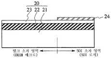
도 2는 본 발명의 제1 실시예에 따른 반도체 장치(10)의 구성예를 나타낸다. 이 구성예는, 도 1b의 A-A' 라인에 따른 단면도로서 도시한다. 도 2의 반도체 장치(10)는 지지 기판(21)과, 지지 기판(21) 상에 형성된 벌크 성장층(26)에 소자가 형성되는 벌크 소자 영역(11)과, 지지 기판(21) 상의 매립 산화막(22) 상에 위치하는 실리콘층(SOI층)(23)에 소자가 형성되는 SOI 소자 영역(12)과, 이들 영역의 경계에 위치하는 경계층인 폴리실리콘층(47)을 구비한다. 도 2의 예는, 벌크 소자 영역(11)은 벌크 성장층으로서, 단결정 Si의 에피택셜 성장층(26)을 구비하고, 지지 기판(21)은, 예를 들면 p형의 실리콘 지지 기판이다.2 shows a configuration example of the
벌크 소자 영역(11)은, 예를 들면 트렌치형 캐패시터(30)를 사용한 DRAM 셀(43), 주변 트랜지스터(44), 그 외에 도시는 하지 않았지만, 필요한 회로 소자를 포함한다. 이들 소자나 회로 전체에서 하나의 기능 블록으로서 DRAM 매크로를 구성한다.The
SOI 소자 영역(12)은, 예를 들면 MOSFET(45)의 어레이를 포함하여, 이들의 고속 소자로 SOI 로직을 구성한다.The
DRAM 셀(43)이나 주변 트랜지스터(44)가 형성되는 에피택셜 성장층(26)의 표면과, MOSFET(45)가 형성되는 SOI층(23)의 표면의 높이는 거의 같다. 따라서, 반도체 칩(10)에 있어서는, 벌크 소자 영역(11) 내의 소자와, SOI 소자 영역(12) 내의 소자는 거의 동일 레벨에 위치하게 된다.The height of the surface of the
DRAM 셀(43), 주변 트랜지스터(44), MOSFET(45)는, 예를 들면 폴리실리콘 등의 실리콘계의 게이트 전극(39a, 41, 39b)을 갖는다. 도 2의 예에서는, 벌크 소자 영역(11)과 SOI 소자 영역(12)의 경계에 위치하는 경계층으로서 폴리실리콘층(47)을 이용하고 있지만, 임의의 실리콘계 재료를 이용할 수 있다. 제조 공정 삭감의 관점에서는, 소자(43, 44, 45)의 게이트 재료로서 이용되는 실리콘계 재료, 예를 들면 실리콘 게르마늄(SiGe) 등의 층인 것이 바람직하다. 이 경우에는, 도시는 하지 않았지만, 경계층(47)이 게이트 절연막을 통해 위치하게 된다.The
또한, 도 2에서는, 폴리실리콘 경계층(47)의 표면이 에피택셜 성장층(26)과 SOI층(23)의 표면보다 약간 내려가 있지만, 은선으로 도시한 바와 같이, 소자(43, 44, 45)의 게이트(39a, 39b, 41)와 동일한 높이까지 돌출하고 있어도 된다.In addition, although the surface of the
반도체 칩(10)은 또, DRAM 매크로가 형성되는 벌크 소자 영역(11) 내에서 각 소자(43, 44)를 분리하는 제1 소자 분리 영역(35a)을 갖고, SOI 로직이 형성되는 SOI 소자 영역(12) 내에 각 소자(45)를 분리하는 제2 소자 분리 영역(35b)을 갖는다. 벌크 소자 영역(11)에 형성되는 제1 소자 분리 영역(35a)과, SOI 소자 영역(12)에 형성되는 제2 소자 분리 영역(35b)은 거의 동일한 깊이이고, 제조 공정 삭감을 위해, 동일한 절연 소재로 매립되는 것이 바람직하다.The
도 2에 도시한 예에서는, SOI층(23)과 매립 산화막(22)을 합한 두께가 비교적 두껍고, SOI 소자 영역(12)에서의 제2 소자 분리 영역(35b)의 깊이는 매립 산화막(22) 도중까지로 되어 있다. 그러나, 매립 산화막(22)이 그만큼 두껍지 않은 경우에는, 제2 소자 분리 영역(35b)의 깊이는, SOI막(23)의 막 두께보다도 깊고, 또한 벌크 소자 영역(11)의 소자 분리 영역(35a)의 깊이와 같은 정도이면, Si 지지 기판(21)에 달하는 깊이어도 괜찮다. 제2 소자 분리 영역(35b)과 제1 소자 분리 영역(35a)을 같은 정도의 깊이로 함으로써, MOSFET(45)가 위치하는 SOI층(23)으로부터, 제2 소자 분리 영역(35b)을 사이에 두고 인접하는 SOI층에 이르는 실효적인 소자 사이 거리가 길어진다. 그 결과로, 매립 산화막(22)의 계면을 통한 누설 전류에 의한 소자 분리 영역 내성의 열화를 피하게 되어, 미세하고 또한 누설 전류가 작은 소자 분리 영역이 가능하게 된다. 제1, 제2 소자 분리 영역이 동일한 깊이, 동일 재료인 경우에는, 동일한 매립 조건으로, 충분한 마진을 갖고 동시 형성이 가능하게 된다.In the example shown in FIG. 2, the sum of the
도 3a∼도 3g는 도 2에 도시한 반도체 장치의 제조 공정을 나타낸다. 이하, 도면에 따라서, 제조 방법을 설명한다.3A to 3G show manufacturing steps of the semiconductor device shown in FIG. 2. Hereinafter, a manufacturing method is demonstrated according to drawing.
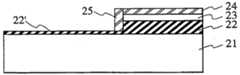
(a) 우선, 도 3a에 도시한 바와 같이, Si 지지 기판(21), 매립 산화막(22), SOI층(23)으로 이루어지는 SOI 웨이퍼(20) 상에, 실리콘 산화막(SiO2)이나 실리콘 질화막(SiN, Si3N4 등), 혹은 이들의 복합막에 의한 마스크 패턴(24)을 형성한다.(a) First, as shown in FIG. 3A, on a
(b) 다음에, 도 3b에 도시한 바와 같이, 마스크 패턴(24)으로 보호되어 있지 않은 영역의 SOI층(23) 및 매립 절연막(22)을, RIE(reactive ion etching) 등의 이방성 에칭에 의해 제거한다. 이 때, Si 지지 기판(21)에의 기계적 손상이나 플라즈마 손상을 막기 위해서, SOI 웨이퍼(20)의 매립 산화막(22')이 조금 남은 상태에서 에칭을 종료한다.(b) Next, as shown in FIG. 3B, the
(c) 다음에, 도 3c에 도시한 바와 같이, 노출된 SOI층(23)의 측면을 보호하기 위해서, 측벽 보호막(25)을 형성한다. 측벽 보호막(25)으로서는, 실리콘 질화막(Si3N4)이나 실리콘 산화막(SiO2)이 적용 가능하다. 이들을 전면에 퇴적시킨 후, RIE에 의해 측벽 잔류를 행하여 측벽 보호막(25)을 형성한다. 측벽 잔류 시에도, 먼저 남긴 매립 산화막(22')이 지지 기판(21) 상에 유지되도록, 측벽 보호막(25)과 지지 기판(21) 상에 남기는 매립 산화막(22')의 막 두께를 조정한다.(c) Next, as shown in FIG. 3C, the sidewall
(d) 다음에, 도 3d에 도시한 바와 같이, 지지 기판(21) 상에 조금 남긴 매립 산화막(22')을, 예를 들면 NH4F나 HF 등의 에칭제를 사용하여 웨트 에칭하여, 지지 기판(21)의 표면을 손상없이 노출시킨다. 소정의 전처리 후에, 예를 들면 화학적 기상 성장에 의한 선택 에피택셜 성장으로, 노출된 지지 기판(21) 상에 단결정 Si층(26)을 형성한다.(d) Next, as shown in FIG. 3D, the buried oxide film 22 'slightly left on the
전공정에서 측벽 보호막(25)에 실리콘 산화막(SiO2)을 사용한 경우에는, 실리콘 기판(21)을 보호하도록 남긴 얇은 매립 산화막(22')을 웨트 에칭할 때에, 측벽 보호막(25)도 약간 에칭된다. 그러나, 지지 기판(21) 표면의 보호를 위해 잔존시킨 매립 산화막(22')의 막 두께를 충분히 얇게 함으로써, SOI층 측벽을 노출시키지 않고, 지지 기판(21)의 표면만을 노출시킬 수 있다.In the case where the silicon oxide film (SiO2 ) is used as the sidewall
한편, 측벽 보호막(25)에 실리콘 질화막(Si3N4)을 사용한 경우에는, 프로세스 제어성이 양호하다. 제1 실시예에서는, 후술하는 바와 같이, 측벽 보호막(25)을 후공정으로 제거하여, 최종적인 제품에서 벌크 소자 영역(11)과 SOI 소자 영역(12)의 경계의 측벽 보호막(25)은 남지 않는다. 따라서, 측벽 보호막(25)에 Si3N4를 사용한 경우라도 응력에 의한 문제는 생기지 않고, 프로세스 제어성을 우선시킬 수 있다.On the other hand, when the side
(e) 다음에, 도 3e에 도시한 바와 같이, SOI 기판 표면에 남는 마스크 패턴(24)을 제거하고, 새롭게 전면에 마스크재(27)를 형성한다. 앞의 마스크 패턴(24)이 Si3N4인 경우에는, 인산에 의해 제거할 수가 있고, 앞의 마스크 패턴(24)이 SiO2인 경우에는, HF(불화 수소)로 제거할 수 있다. 이 때, 측벽 보호막(25)도 마스크 패턴(24)의 에칭에 의해 적어도 일부 에칭되지만, 그 부분도 마스 크재(27)로 매립되게 된다. 새롭게 형성하는 마스크재(27)도, SiO2, SiNx, 혹은 이들의 복합막이다. 마스크재(27)를 패터닝하고 이것을 마스크로 하여, DRAM의 트렌치 캐패시터(30)를 형성한다. 트렌치 캐패시터(30)는 원하는 방법으로 형성할 수 있다. 예를 들면, RIE 등으로 트렌치를 형성한 후, 하부 확산 플레이트(31)를 형성하고, 유전막(도시되지 않음)을 통해 n형 폴리실리콘 등의 축적 전극(29)을 매립한다. 컬러 절연막(32)을 형성하고, 트렌치를 더 매립하고, 상부에 셀 트랜지스터의 한쪽의 n형 소스/드레인 확산층(40a)(도 2 참조)에 전기적으로 접속하기 위한 스트랩(33)을 형성하고, 최종적으로 n형 폴리실리콘 등으로 매립한다.(e) Next, as shown in FIG. 3E, the
(f) 다음에, 도 3f에 도시한 바와 같이, 소자 분리 영역(35a, 35b)을, 벌크 소자 영역(11)과 SOI 소자 영역(12)의 쌍방에 일괄하여 형성한다. 구체적으로는, 마스크재(27)를 패터닝하고, 소자 분리 영역용의 얕은 트렌치를, 벌크 소자 영역(11)과 SOI 소자 영역의 양방에 동일한 깊이로 형성한다. 마스크재(27)를 스토퍼로 하여 트렌치 내에 절연막을 매립하여, 벌크 소자 영역(11)의 제1 소자 분리 영역(35a)과 SOI 소자 영역(12)의 제2 소자 분리 영역(35b)을 동시에 형성한다.(f) Next, as shown in FIG. 3F, the
실리콘층과, 실리콘 산화막을 동등한 에칭 속도로 에칭할 수 있는 조건을 설정하여, SOI 소자 영역(12)의 소자 분리 영역용 트렌치와, 벌크 소자 영역(11)의 소자 분리 영역용 트렌치를 동일한 레이트로, DRAM셀의 스트랩(33) 사이와 주변 회로와 SOI 소자의 모든 소자 분리 영역에 필요한 깊이까지 홈을 파고, 동일한 절연 재료를 충전한다. 이에 따라, 벌크 소자 영역(11)의 제1 소자 분리 영역(35a)과, SOI 소자 영역(12)의 제2 소자 분리 영역(35b)이 일괄 형성된다.The silicon layer and the conditions in which the silicon oxide film can be etched at the same etching rate are set so that the trench for device isolation region of the
(g) 마지막으로, 도 3g에 도시한 바와 같이, 트렌치 내의 매립 절연막을 SOI층(23)이나 에피택셜 성장층(26)의 표면까지 에치백하여, 마스크재(27)를 제거한다. 마스크재(27)를 제거할 때에, 혹은 새로운 에칭 공정에 의해 측벽 보호막(25)의 적어도 일부를 제거하여, 오목부(46)를 형성한다. 오목부(46)를 실리콘계 재료로 매립함으로써 도 2에 도시한 경계층(47)을 형성한다. 오목부(46)의 매립은 독립된 공정으로 행해도 되며, 게이트 전극(39, 41)의 제작과 동시에 매립해도 된다. 전자의 경우에는, 오목부(46)를 매립한 후, 웰이나 채널의 도핑을 필요에 따라 행하여, 소정의 위치에 게이트 절연막(48)을 통한 게이트 전극(39, 41)(도 2 참조)과, 소스·드레인(40, 42)을 형성한다. 후자의 경우에는 게이트 전극을 폴리실리콘이나 SiGe 등의 실리콘계 재료로 형성함으로써, 게이트 전극 형성 시에, 오목부(46)가 자동적으로 게이트 재료로 매립된다. 이 결과, SOI층(23)과 Si 단결정의 에피택셜 성장층(26)의 경계가 동일한 실리콘계 막(47)으로 연결된다.(g) Finally, as shown in FIG. 3G, the buried insulating film in the trench is etched back to the surface of the
도 2에 도시한 게이트 전극(39, 41)의 형성 후에, 원하는 MOSFET 형성 공정에 따라서 층간 절연막이나 배선공정을 거쳐, DRAM 매크로와 SOI 로직을 혼재한 반도체 장치가 완성된다. 소자 형성 시에, 게이트 전극 상이나 소스·드레인 상에의 살리사이드 프로세스를 이용하는 경우에는 경계에 매립된 폴리실리콘(47)의 변형을 방지하기 위해서, 폴리실리콘(47)을 마스크 등으로 보호하는 것이 바람직하다.After the formation of the
도 2의 일점쇄선으로 도시한 바와 같이, 경계층(47)을 패턴으로서 돌출시키는 경우에는, 오목부(46) 자체는 폴리실리콘으로 보호되어 있기 때문에, 살리사이 드를 행하는 것도 가능하게 된다.As shown by the dashed-dotted line of FIG. 2, when projecting the
또, 도 2에 도시한 예에서는, SOI층(23)과 매립 산화막(22)을 합한 두께가 비교적 두껍고, 지지 기판(21)과 에피택셜 성장층(26)의 계면이 비교적 깊은 위치에 설정된다. DRAM 메모리 셀(43)의 스트랩부(33)의 pn 접합면이나 셀부의 소스·드레인(40a, 40b)을 지지 기판(21)과 에피택셜 성장층(26)의 계면에서 확실하게 분리하기 위해서, 이 pn 접합면을 계면보다도 얕은 위치에 형성하고 있다. 가령 프로세스 불량으로 계면 상태가 열화한다고 해도, 접합 누설을 방지하여 메모리 셀의 보유 특성을 유지하기 때문이다.In addition, in the example shown in FIG. 2, the thickness of the
제1 실시예의 반도체 장치에서는, 벌크 소자 영역(11)의 에피택셜 성장층(26)과 SOI층(23) 사이를, 폴리실리콘, SiGe 등의 실리콘계 재료로 연결함으로써, 영역 사이의 경계에서의 응력에 의한 결정 결함을 억제할 수 있다.In the semiconductor device of the first embodiment, the stress at the boundary between the regions is connected by connecting the
또한, 영역 사이의 응력에 의한 이동도의 변동을 방지할 수 있어, 경계 근방의 소자의 열화를 효과적으로 방지할 수 있다.In addition, fluctuation in mobility due to stress between regions can be prevented, and deterioration of the element near the boundary can be effectively prevented.
또한, 본래 SOI층의 측벽을 보호하는 측벽 보호막이 있는 위치에 경계층을 형성하기 때문에, 칩 면적 증대를 억제할 수 있다.In addition, since the boundary layer is formed at the position where the sidewall protective film that originally protects the sidewall of the SOI layer is formed, the chip area increase can be suppressed.
벌크 소자 영역과 SOI 소자 영역의 소자 형성면이 균일한 높이에 있기 때문에, 게이트 전극의 리소그래피 등, 후공정에 유리하다.Since the element formation surfaces of the bulk element region and the SOI element region are at a uniform height, they are advantageous for post-processing such as lithography of the gate electrode.
SOI 소자 영역의 소자 분리 영역이, 트렌치 캐패시터를 갖는 벌크 소자 영역의 소자 분리 영역과 같은 정도의 깊이를 갖기 때문에, SOI 소자 영역측의 소자 분리 영역은, 표면적으로서는 미세함에도 불구하고 누설 전류를 효과적으로 방지할 수 있다. 또한, 소자 분리 영역의 매립 조건을 충분한 마진을 갖고 형성할 수 있다.Since the element isolation region of the SOI element region has the same depth as the element isolation region of the bulk element region having the trench capacitor, the element isolation region on the side of the SOI element region effectively prevents leakage current despite being fine on the surface. can do. In addition, the embedding conditions of the element isolation regions can be formed with sufficient margin.
도 2에 도시한 바와 같이 SOI 로직과 DRAM을 동일 칩 상에 탑재한 시스템 온 칩형 반도체 장치는, 로직과 DRAM을 별개의 칩으로 한 경우에 비하여 고속, 저소비 전력으로 데이터를 교환할 수 있다.As shown in FIG. 2, a system-on-chip semiconductor device in which SOI logic and DRAM are mounted on the same chip can exchange data at higher speed and lower power consumption than when the logic and DRAM are separate chips.
또한, 벌크 소자 영역(11)은 DRAM 메모리 셀(43)뿐만이 아니라, 주변 회로(44)나 그 밖의 회로 소자도 포함한 하나의 기능 블록(DRAM 매크로)을 포함함으로써, 본래 벌크 기판으로 개발된 DRAM의 회로 설계나 디바이스 설계를 그대로 SOI/벌크 기판에 적용할 수 있다. 물론, DRAM 매크로뿐만이 아니라, 벌크 기판을 이용하여 개발된 그 밖의 기능 매크로, 예를 들면 아날로그 회로 매크로, 고내압 회로 매크로, DRAM 이외의 메모리 회로 매크로 등에도 적용 가능하다.In addition, the
제1 실시예의 제조 방법에서는, 소자 형성면의 높이가 거의 같은 벌크 소자 영역과 SOI 소자 영역의 소자 분리 영역을 동일한 트렌치 깊이로 일괄하여 형성하고 있다. 따라서, 매립에 필요한 절연막의 막 두께나 매립 시의 에치백 시간 등의 프로세스 조건에도 거의 차가 생기지 않고, 소자 분리 영역의 형성 작업이 간이하게 된다.In the manufacturing method of the first embodiment, the bulk element region and the element isolation region of the SOI element region are formed in the same trench depth at the same time as the element formation surface is almost the same height. Therefore, almost no difference occurs in the process conditions such as the film thickness of the insulating film required for embedding and the etchback time at the time of embedding, and the work for forming the element isolation region is simplified.
<제2 실시예>Second Embodiment
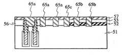
도 4는 본 발명의 제2 실시예에 따른 반도체 장치(50)의 개략 단면도이다. 반도체 장치(50)는 지지 기판(51)과, 지지 기판(51) 상에 형성된 에피택셜 성장층(56)에 소자(43, 44)가 형성되는 벌크 소자 영역(11)과, 지지 기판(51) 상의 매립 산화막(52) 상에 위치하는 SOI층(53)에 소자(45)가 형성되는 SOI 소자 영역(12)과, 벌크 소자 영역 내의 각 소자(43, 44)를 분리하는 제1 소자 분리 영역(65a)과, SOI 소자 영역(12) 내의 각 소자(45)를 분리하는 제2 소자 분리 영역(65b)과, 벌크 소자 영역(11)과 SOI 소자 영역(12)의 경계에 위치하는 제3 소자 분리 영역(65c)을 갖는다. 이 예에서는, 제3 소자 분리 영역(65c)이 경계층이 된다.4 is a schematic cross-sectional view of a
제2 실시예에 있어서도, 벌크 소자 영역(11)에 형성되는 소자(43, 44), 그 밖의 회로 소자(도시되지 않음)로 DRAM 매크로를 구성하고, SOI 소자 영역(12)에 형성되는 소자(45)로 SOI 로직을 구성하는 것으로 한다.Also in the second embodiment, a DRAM macro is composed of the
제1∼제3 소자 분리 영역(65a∼65c)은 전부 동일한 깊이로 설정되고, 또한 SOI 소자 영역(12)의 매립 산화막(52)보다도 깊다. 또한, DRAM 셀(43) 등이 형성되는 벌크 소자 영역(11)의 소자 형성면과, MOSFET(45)가 형성되는 SOI 소자 영역(12)의 소자 형성면은 거의 균일한 높이에 있고, DRAM 매크로를 구성하는 소자(43, 44)와, SOI 로직을 구성하는 소자(45)는 거의 동일한 높이에 위치한다.The first to third
벌크 소자 영역(11)은 벌크 성장층으로서 단결정 Si의 에피택셜 성장층(56)을 갖는다. SOI 소자 영역(12)은 실리콘 지지 기판(51)과, 매립 산화막(52)과, SOI막(53)으로 구성되고, 매립 산화막(52)과 SOI층(53)의 합한 두께는 제1 실시예에 비하여 약간 작게 설정되어 있다. 매립 산화막(52)을 얇게 함으로써, SOI 소자의 동작에 의한 발열을 효율적으로 지지 기판(51)으로 발산시켜, 소자 특성의 열화를 방지한 후에 필요하게 되는 경우가 있다.The
제2 실시예에 따른 반도체 장치(50)는, 벌크 소자 영역(11)과 SOI 소자 영역(12) 각각에 배치되는 소자 분리 영역과 마찬가지의 깊이, 소재의 소자 분리 영역(65c)을, 경계부에 갖는다. 경계에 위치하는 소자 분리 영역(65c)은 그 밖의 소자 분리 영역(65a, 65b)과 마찬가지로 매립 산화막(53)보다도 깊다. 따라서, 경계 부분에서 전위 등의 결함이 벌크 소자 영역의 에피택셜 성장층(56)으로 넓어지는 것을 방지할 수 있다.The
도 5a∼도 5c는 도 4에 도시한 반도체 장치(50)의 제조 공정을 도시하는 도면이다. 도 5a는 도 3d에 이어지는 공정도로, 도 3a∼도 3d까지의 공정은 매립 산화막의 막 두께가 다른 것 이외는 제1 실시예와 공통되기 때문에, 그 설명의 상세는 생략한다.5A to 5C are diagrams showing manufacturing steps of the
제1 실시예에서는 측벽 보호막을 제거하여 영역 간의 경계 부분을 실리콘계 재료로 연결함으로써 응력의 문제를 해결하였다. 그러나, 이는, 측벽 보호막과 접하는 에피택셜층이 손상을 받고 있는 경우에는 불완전한 처치가 된다.In the first embodiment, the problem of stress was solved by removing the sidewall protective film to connect the boundary portions between the regions with a silicon-based material. However, this is incomplete treatment when the epitaxial layer in contact with the sidewall protective film is damaged.
그래서, 제2 실시예의 제조 방법에서는, 매립 산화막의 두께가 비교적 얇은 SOI 기판을 준비하고 소자 분리 영역용의 트렌치를 깊게 하는 등으로 하여, 소자 분리 영역의 깊이를 SOI 소자 영역의 매립 산화막보다도 깊게 설정한다. 또한, 벌크 소자 영역(11)과 SOI 소자 영역(12)의 경계부에도 소자 분리 영역용 트렌치를 배치함으로써, 각 영역 내의 소자 분리 영역 트렌치의 형성과 동시에, 경계에 남아 있던 측벽 보호막과 경계 부근에서 결정성이 열화한 부분을 한꺼번에 제거한다.Therefore, in the manufacturing method of the second embodiment, an SOI substrate having a relatively small thickness of the buried oxide film is prepared, and the trench for the device isolation region is deepened, and the depth of the device isolation region is set deeper than that of the buried oxide film in the SOI device region. do. In addition, by arranging the trenches for device isolation regions at the boundary between the
구체적으로는, 도 5a에 도시한 바와 같이, 벌크 소자 영역의 에피택셜 성장층(56), SOI 기판의 SOI층(53), 측벽 보호막(55)의 전면을 덮어서 마스크재(57)를 형성한다. 마스크재(57)를 소정의 형상으로 패터닝한 후, 제1 실시예와 마찬가지로, DRAM의 트렌치 캐패시터(30)를 형성한다.Specifically, as shown in FIG. 5A, the
다음에 도 5b에 도시한 바와 같이, 벌크 소자 영역, SOI 소자 영역, 및 이들의 경계에, 일괄하여 소자 분리 영역용 트렌치를 형성한다. 이 때, 실리콘, 폴리실리콘, 및 실리콘 산화막에 대하여 동등한 에칭 레이트를 갖는 에칭 조건을 설정함으로써, 동일한 에칭 시간에 동일한 깊이의 트렌치를 일괄하여 형성할 수 있다. 또, 어느 하나의 트렌치도 SOI 소자 영역의 매립 산화막(52)보다도 깊다. 잔존하고 있는 측벽 보호막(55)의 깊이는 겨우 매립 산화막(52)의 깊이 정도이기 때문에, 소자 분리 영역 트렌치의 형성과 동시에, 측벽 보호막(55)과 경계 부분에 결정성이 열화한 영역이 함께 제거된다. 그 후, 트렌치 내를 동일한 절연 소재로 매립함으로써, 벌크 소자 영역(DRAM 매크로)의 제1 소자 분리 영역(65a), SOI 소자 영역(SOI 로직)의 제2 소자 분리 영역(65b) 및 경계에 위치하는 제3 소자 분리 영역(65c)을 일괄 형성할 수 있다.Next, as shown in Fig. 5B, trenches for element isolation regions are collectively formed in the bulk element region, the SOI element region, and their boundaries. At this time, by setting etching conditions having the same etching rate for silicon, polysilicon, and silicon oxide film, trenches of the same depth can be collectively formed at the same etching time. Further, either trench is deeper than the buried
그 후, 도 5c에 도시한 바와 같이, 트렌치 내의 매립 절연막을 에치백하여, 마스크재(57)를 제거하고, 소정의 위치에 소자(43, 44, 45)를 형성하여, 도 4에 도시한 반도체 장치(50)가 완성된다.Thereafter, as shown in Fig. 5C, the buried insulating film in the trench is etched back, the
제2 실시예에 따른 반도체 장치와, 그 제조 방법에서는, 경계에 위치하는 소자 분리 영역(65c)이 매립 산화막(53)보다도 깊고, 측벽 보호막(55)과 그 이웃하는 결정 열화 부분이 함께 제거된다. 이에 따라 응력을 완화함과 함께, 응력의 영향에 의해 경계부로부터 전위 등의 결함이 에피택셜 성장층(56)으로 넓어지는 것을 방지할 수 있다.In the semiconductor device and the manufacturing method thereof according to the second embodiment, the
또한, 종래의 소자 분리 영역 구조를 영역 사이의 경계에 그대로 적용할 수 있다는 장점도 있다.In addition, there is an advantage that the conventional device isolation region structure can be applied as it is to the boundary between regions.
칩 면적 증대의 효과적인 억제, 소자 형성면의 높이의 균일화에 의한 효과는, 제1 실시예와 마찬가지이다.The effect of effective suppression of chip area increase and uniformity of the height of the element formation surface is the same as in the first embodiment.
<제3 실시예>Third Embodiment
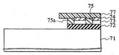
도 6은 본 발명의 제3 실시예에 따른 반도체 장치(70)의 개략 단면도이다. 반도체 장치(70)는, DRAM 셀(83)이나 주변 트랜지스터(84)가 형성되는 벌크 소자 영역(11)과, MOSFET(85)가 형성되는 SOI 소자 영역(12)과, 벌크 소자 영역(11)에 형성되는 제1 소자 분리 영역(79)과, SOI 영역(12)에 형성되는 제2 소자 분리 영역(75, 75a)을 구비하고, 제2 소자 분리 영역(75, 75a)은 제1 소자 분리 영역(79)보다도 얕다.6 is a schematic cross-sectional view of a
벌크 소자 영역(11)과 SOI 소자 영역(12) 중 어느 하나의 소자 분리 영역 중, 가장 경계 근방에 위치하는 소자 분리 영역(75a)이 영역 사이의 경계층을 겸용한다. 도 7의 예에서는, SOI 소자 영역(12)에 위치하는 제2 소자 분리 영역 중, 가장 경계측의 소자 분리 영역(75a)은, 벌크 소자 영역(11)과 SOI 소자 영역(12) 사이에 위치하는 경계를 겸하고 있고, 소자 분리 영역층(75a)의 저면에서, SOI 소자 영역(12)의 매립 산화막(72)과 접하고 있다. 물론, 설계에 따라서, 벌크 소자 영역(11)의 가장 경계측에 위치하는 소자 분리 영역(79)이 경계층을 겸용해도 된다. 이 경우에는, 도시는 하지 않았지만, 경계가 되는 소자 분리 영역(79)이 SOI 소자 영역(12)의 단부의 소자 분리 영역(75a) 및 그 하방의 매립 산화막(79)에 오버랩하게 된다.Among the element isolation regions of any one of the
벌크 소자 영역(11)은 벌크 성장층으로서 에피택셜 성장층(76)을 갖고, DRAM 셀(83), 주변 트랜지스터(84), 및 그 밖의 회로 소자(도시되지 않음)에서 DRAM 매크로를 구성한다. SOI 소자 영역(12)은 SOI층(73), 매립 산화막(72) 및 실리콘 지 지 기판(71)으로 이루어지고, MOSFET(85)로 SOI 로직을 구성한다. 이들 소자는, 벌크 소자 영역(11)과 SOI 소자 영역(12)을 통해서 균일한 높이에 위치한다.The
이와 같이, 제3 실시예에 따른 반도체 장치(70)에서는 벌크 소자 영역(11)과 SOI 소자 영역(12)으로, 각각의 영역에 따른 최적의 소자 분리 영역을 설정하기 위해서, 제1 소자 분리 영역(79)의 깊이와 제2 소자 분리 영역(75)의 깊이가 다르다. 또한, 어느 하나의 영역의 소자 분리 영역 중, 가장 경계의 근방에 위치하는 소자 분리 영역(도 7의 예에서는 SOI 소자 영역의 소자 분리 영역(75a))이 벌크 소자 영역(11)과 SOI 소자 영역(12)의 영역 간의 경계층을 겸용한다.As described above, in the
제3 실시예의 반도체 장치(70)에 있어서, 벌크 소자 영역(11)과 SOI 소자 영역(12)의 각각에, 최적의 깊이의 소자 분리 영역을 형성하는 이유는 이하와 같다.In the
제1 실시예 및 제2 실시예에서는, 모든 소자 분리 영역을 동일한 구성으로 하고 있었지만, 로직부에서는 특히 소자 분리 영역의 미세화가 요구되는 경우가 있다. 고도의 미세화가 요구되는 경우에, SOI 기판에 매립 산화막보다 깊은 트렌치를 형성하기 위해서는, SOI층의 측벽을 에칭할 때의 트렌치의 테이퍼각과, 매립 산화막의 측벽을 에칭할 때의 트렌치의 테이퍼각을, 정밀하게 제어해야만 한다. 각도 제어를 정밀하게 행하지 않으면, 트렌치를 매립한 후에, 내부에 공동이 남고, 공동 내에 게이트 전극재가 잔존하여 배선 쇼트 불량을 야기할 우려가 있기 때문이다.In the first embodiment and the second embodiment, all the device isolation regions have the same configuration, but in the logic section, the device isolation region may be particularly small. When a high degree of miniaturization is required, in order to form a trench deeper than the buried oxide film in the SOI substrate, the taper angle of the trench when etching the sidewall of the SOI layer and the taper angle of the trench when etching the sidewall of the buried oxide film It must be precisely controlled. This is because if the angle control is not performed precisely, a cavity remains inside after the trench is filled, and a gate electrode material remains in the cavity, which may cause wiring short defects.
그래서, 특히 로직부에서의 미세화가 요구되는 경우에, SOI 소자 영역에 최적의 소자 분리 영역을 형성함으로써, 응력 완화, 소자 면적 증대의 효과적인 억제, 소자 형성면의 높이의 균일화라는 효과 외에 배선 쇼트 불량 등을 방지하여, 동작의 신뢰성을 확보한다.Therefore, in the case where miniaturization is required in the logic section, by forming an optimum device isolation region in the SOI device region, wiring short defects are in addition to the effects of stress relaxation, effective suppression of device area increase, and uniformity of the element formation surface. Etc., to ensure the reliability of the operation.
반도체 장치(70)에서는, 벌크 소자 영역(11)과 SOI 소자 영역(12) 중 어느 하나의 영역의 소자 분리 영역이 경계부에서 경계층으로서 기능한다. 따라서, 경계의 바로 옆에까지 소자를 형성하는 것이 가능하게 되어, 무효 공간이 축소하여, 칩 면적의 증대를 효율적으로 억제할 수 있다.In the
또한, 벌크 소자 영역(11)과 SOI 소자 영역(12) 각각에, 최적의 소자 분리 영역을 배치함으로써, SOI 소자 영역의 소자 분리 영역 내부에서의 공동의 발생을 방지하여, 게이트 전극의 단락 등을 억제할 수 있다.In addition, by arranging an optimal element isolation region in each of the
도 7a∼도 7f는 제3 실시예에 따른 반도체 장치(70)의 제조 공정을 도시하는 도면이다.7A to 7F are diagrams showing manufacturing steps of the
(a) 우선, 도 7a에 도시한 바와 같이, SOI 소자 영역(12) 내의 소정 위치와 벌크 소자 영역의 경계에서 쌍방의 영역에 걸치는 위치에, 얕은 소자 분리 영역(75, 75a)을 형성한다. 보다 구체적으로는, SOI 기판 전면에 실리콘 질화막 등의 마스크재를 퇴적하고, 이것을 패터닝하여 제1 마스크(74)를 형성한다. 제1 마스크(74)에 덮여진 이외의 위치에 RIE 등에 의해 얕은 트렌치를 형성하고, SiO2 등의 절연막을 퇴적하여 소자 분리 영역(75, 75a)을 형성한다. 이들 소자 분리 영역(75, 75a)이 SOI 소자 영역에 위치하는 제2 소자 분리 영역이 된다.(a) First, as shown in FIG. 7A, shallow
(b) 다음에, 도 7b에 도시한 바와 같이, 레지스트 등으로 전면에 제2 마스크재(77)를 형성하여 SOI 소자 영역 전체와 경계에 위치하는 소자 분리 영역(75a)이 덮여지도록, 제2 마스크재(77)를 패터닝한다. 이 제2 마스크재(77)를 마스크로 하여, 제1 마스크재(74), SOI층(73), 경계의 소자 분리 영역(75a)의 일부, 및 매립 산화막(72)을 순차 에칭 제거한다. 바람직하게는, 제1 마스크재(74), SOI층(73), 소자 분리 영역(75a)과, 매립 산화막(73)의 도중까지를, 예를 들면 RIE에 의해 제거하고, 최종적으로 실리콘 지지 기판(71)을 노출할 때에는, 웨트 에칭으로 한다.(b) Next, as shown in FIG. 7B, the
RIE에 의한 에칭 시에는 SOI 소자 영역의 SOI층(73)의 측면은, 일부러 측벽 보호막을 형성하지 않아도, 경계에 위치하는 제2 소자 분리 영역(75a)에 의해 보호되어 있다. 또한, 매립 산화막(72)과, 경계에 위치하는 제2 소자 분리 영역(75a)이 함께 SiO2계의 복합막이기 때문에, 최종적으로 벌크 소자 영역의 실리콘 지지 기판(71)을 노출시키는 단계에서 웨트 처리로 한다. 이 웨트 에칭에 의해, 지지 기판(71)에 손상을 끼치는 일 없이, 매립 산화막(72)과 제2 소자 분리 영역(75a) 중 벌크 소자 영역측에 돌출하는 부분을 제거할 수 있다.At the time of etching by RIE, the side surface of the
(c) 다음에, 도 7c에 도시한 바와 같이, 제2 마스크재(77)를 제거하고, 노출된 실리콘 지지 기판(71) 상에 단결정 실리콘을 선택 에피택셜 성장시켜, 에피택셜 성장층(76)을 형성한다. 이에 따라, SOI 기판 내에 벌크 소자 영역이 형성된다.(c) Next, as shown in FIG. 7C, the
(d) 다음에, 도 7d에 도시한 바와 같이, 필요하면 제1 마스크 패턴(74)을 제거한 후, 새롭게 마스크재(78)를 전면에 형성하고 패터닝하여, 벌크 소자 영역에 트렌치 캐패시터(30)를 형성한다. 트렌치 캐패시터(30)의 형성 방법은 제1 실시예에서 설명한 바와 같다.(d) Next, as shown in FIG. 7D, the
(e) 다음에, 도 7e에 도시한 바와 같이, 벌크 소자 영역에 제2 소자 분리 영역(75)보다도 깊은 제1 소자 분리 영역(79)을 형성한다.(e) Next, as shown in FIG. 7E, the first
(f) 마지막으로, 도 7f에 도시한 바와 같이, 트렌치 내의 매립 절연막을 에치백하여, 마스크재(78)의 제거 후에, DRAM과 SOI 로직을 구성하는 트랜지스터(83, 84, 85)를 형성하여 반도체 장치(70)가 완성된다.(f) Finally, as shown in FIG. 7F, the buried insulating film in the trench is etched back, and after removal of the
도 8a∼도 8c는 도 6에 도시한 반도체 장치(70)의 다른 제조 공정을 나타내는 도면이다. 도 7에 도시한 제조 공정에서는, 벌크 소자 영역의 형성에 있어서, SOI 소자 영역 내와 경계 상에만 얕은 소자 분리 영역(75, 75a)을 형성하고, 벌크 소자 영역이 될 예정의 SOI 기판 상에는 마스크재(74)를 남겨 놓았다. 도 8에 도시한 제조 공정에서는, 결정 성장에 의해 벌크화할 예정의 영역 전체에, 소자 분리 영역층(75a)을 사전에 형성한다.8A to 8C are views showing another manufacturing process of the
우선, 도 8a에 도시한 바와 같이, 제1 마스크재(74)를 전면에 퇴적한 후, SOI 소자 영역(12) 내의 소자 형성 부분만을 덮도록 패터닝한다. 그 밖의 부분, 즉, SOI 소자 영역(12) 내의 일부(소자 분리 영역이 되는 영역)와, 벌크화하는 영역의 전체에, 예를 들면 SiO2의 소자 분리 영역용 절연막(75, 75a)을 형성한다.First, as shown in FIG. 8A, the
다음에, 도 8b에 도시한 바와 같이, 제2 마스크재(77)를, SOI 소자 영역과, 벌크화하는 영역 중 경계에 접하는 부분 상에 남도록 패터닝한다. 그리고, 벌크 성장층을 형성하는 영역의 소자 분리 영역용 절연막(75a)과 매립 산화막(72)을, 바람직하게는 웨트 에칭에 의해 한번에 제거한다. 이에 따라, SOI 영역의 SOI층(73)의 측벽을 자동적으로 보호한 상태에서 한번의 에칭으로 실리콘 지지 기판(71)을 노출할 수 있다. 또한, 소자 분리 영역 절연막(75)과 매립 산화막(75a)의 쌍방을 연속적으로 웨트 제거하기 때문에, 실리콘 지지 기판(71)의 표면에 손상을 끼치지 못한다.Next, as shown in FIG. 8B, the
다음에, 도 8c에 도시한 바와 같이, 노출된 실리콘 지지 기판(71) 상에 선택 에피택셜 성장으로 에피택셜 성장층(76)을 형성한다.Next, as shown in FIG. 8C, the
이후의 공정에 대해서는, 도 7d∼도 7f와 마찬가지이다. 도 8에 도시한 제조 방법으로는, 벌크 영역의 실리콘 지지 기판을 노출할 때에, 한번의 웨트 에칭으로 된다. 이 때문에, 가령 벌크 소자 영역과 SOI 소자 영역에, 각각 다른 깊이, 다른 소재의 소자 분리 영역을 형성한다고 해도, 전체적으로 보면 제조 공정은 간략화된다.About a subsequent process, it is the same as FIG. 7D-7F. In the manufacturing method shown in FIG. 8, when exposing the silicon support substrate of a bulk area | region, it becomes one wet etching. For this reason, even if the element isolation regions of different depths and different materials are formed in the bulk element region and the SOI element region, for example, the manufacturing process is simplified as a whole.
도 7 및 도 8에 도시한 어느 하나의 제조 방법에 있어서도, SOI 소자 영역의 소자 분리 영역 형성 후에, 고온 공정을 수반하는 에피택셜 성장이나 트렌치 캐패시터 형성을 행하기 위해서 프로세스의 최적화에 의해, SOI 소자 영역의 응력을 완화하는 것을 기대할 수 있다.In any of the manufacturing methods shown in FIGS. 7 and 8, after the isolation region of the SOI element region is formed, the SOI element is optimized by optimizing the process to perform epitaxial growth and trench capacitor formation involving a high temperature process. It can be expected to relieve stress in the region.
또한, 벌크 소자 영역과 SOI 소자 영역의 쌍방에 걸쳐, 균일한 높이로 소자를 형성할 수 있다.In addition, an element can be formed at a uniform height over both the bulk element region and the SOI element region.
또한, 경계부에 사전에, 벌크 소자 영역과 SOI 소자 영역 중 어느 하나에 속하는 소자 분리 영역(75a)을 형성함으로써, SOI층의 측면을 자동적으로 보호할 수 있다. 따라서, 독립된 측벽 보호막의 형성 공정이 불필요하게 된다.In addition, the side of the SOI layer can be automatically protected by forming the
벌크 소자 영역부의 지지 기판을 노출시킴에 대응하여, 매립 산화막과 경계부에 위치하는 소자 분리 영역용 절연막의 쌍방을 웨트 처리로 에칭 가능하기 때문에, 지지 기판에의 손상을 피할 수 있다.In response to exposing the supporting substrate of the bulk element region portion, both the buried oxide film and the insulating film for element isolation region located at the boundary portion can be etched by wet processing, so that damage to the supporting substrate can be avoided.
<제4 실시예>Fourth Example
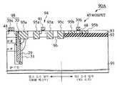
도 9a 및 도 9b는 본 발명의 제4 실시예에 따른 반도체 장치를 나타낸다. 제4 실시예에서는, 제2 실시예와 제3 실시예를 조합, 경계부에 매립 산화막보다 깊은 독립한 소자 분리 영역을 배치하여, 측벽 보호막마다 경계부의 결정 결함을 모두 제거함과 동시에, 각 영역에 최적의 소자 분리 영역을 형성한다.9A and 9B show a semiconductor device according to a fourth embodiment of the present invention. In the fourth embodiment, in combination with the second embodiment and the third embodiment, an independent element isolation region deeper than the buried oxide film is disposed at the boundary portion, so that all the crystal defects at the boundary portion are removed for each sidewall protective film, and optimal for each region. To form a device isolation region.
도 9a의 예에서는, 반도체 장치(90A)는 지지 기판(91)과, 지지 기판(91) 상에 형성된 에피택셜 성장층(96)에 소자(98, 94)가 형성되는 벌크 소자 영역(11)과, 지지 기판(91) 상의 매립 산화막(92) 상에 위치하는 SOI층(93)에 소자(45)가 형성되는 SOI 소자 영역(12)을 구비한다. 또한, 벌크 소자 영역(11) 내의 각 소자(98, 94)를 분리하는 제1 소자 분리 영역(95a)과, SOI 소자 영역(12) 내의 각 소자(45)를 분리하는 제2 소자 분리 영역(95b)과, 벌크 소자 영역(11)과 SOI 소자 영역(12)의 경계에 위치하는 제3 소자 분리 영역(95c)을 갖는다. SOI 소자 영역 내의 제2 소자 분리 영역(95b)은 벌크 소자 영역(11) 내의 제1 소자 분리 영역(95a) 및 경계에 위치하는 제3 소자 분리 영역(95c)보다도 얕다. 경계부의 제3 소자 분리 영역(95c)은 SOI 소자 영역(12)의 매립 산화막(92)보다도 깊다.In the example of FIG. 9A, the
또한, DRAM 셀(98) 등이 형성되는 벌크 소자 영역(11)의 소자 형성면과 MOSFET(45)가 형성되는 SOI 소자 영역(12)의 소자 형성면은 거의 균일한 높이에 있고, DRAM 매크로를 구성하는 소자(98, 94)와 SOI 로직을 구성하는 소자(45)는 거의 동일한 높이에 위치한다.In addition, the element formation surface of the
도 9a에 도시한 반도체 장치(90A)를 제작하기 위해서는, DRAM의 트렌치 캐패시터(30)의 제조 공정까지는, 도 3a∼도 3e와 마찬가지로, 그 후, 벌크 소자 영역(11)의 제1 소자 분리 영역(95a)과 경계부에 위치하는 제3 소자 분리 영역(95c)을 동일한 리소그래피 공정으로 형성하여, 일거에 측벽 보호막을 제거하고, SOI 소자 영역(12) 내의 제2 소자 분리 영역(95b)을 다른 리소그래피 공정으로 형성하면 된다. 도 9a의 예는, 경계에 위치하는 제3 소자 분리 영역(95c)이 SOI층(93) 측에 다소 들어가 있지만, 에칭 조건에 따라서는, 매립 산화막(92) 측에 들어가는 경우도 있다. 또한, SOI 소자 영역(12)의 단부의 제2 소자 분리 영역(95b)을 경계에 근접하여 형성하는 경우에는 제3 소자 분리 영역(95c)과 경계 근방의 제2 소자 분리 영역(95b)이 일체가 되어도 된다.In order to manufacture the
도 9b에 도시한 반도체 장치(90B)는 벌크 소자 영역(11) 내의 DRAM 셀(98)을 분리하는 제1 소자 분리 영역(97a)과 SOI 소자 영역(12) 내의 제2 소자 분리 영역(97b)을 같은 정도의 깊이로 하고, 경계에 위치하는 제3 소자 분리 영역(97c)보다도 얕게 설정한다. 경계부의 소자 분리 영역(97c)은 에피택셜 성장 시의 결정 결함마다 제거하기 위해서, 매립 산화막(92)보다도 깊게 설정할 필요가 있다. 한편, 트렌치 캐패시터(30)의 축적 전극(29)의 인출 저항을 저감하기 위해서, 제1 소자 분리 영역(97a)을 SOI 소자 영역(12)의 MOSFET(45)를 분리하는 제2 소자 분리 영역(97b)과 같은 정도로 얕게 형성한다. 이에 따라, 영역마다 보다 적절한 소자 분리 영역이 가능하게 된다. 또, 벌크 소자 영역(11) 내의 주변 회로(44)의 소자 분리 영역(97d)은 경계부의 제3 소자 분리 영역(97c)과 동시에, 동일한 깊이, 동일한 소재로 형성해도 되고, 혹은 DRAM 셀의 제1 소자 분리 영역(97a)이나 SOIMOSFET(45)의 제2 소자 분리 영역(97b)과 동시에 형성해도 된다.The
도 9a, 도 9b 중 어느 예에서도, 벌크 소자 영역 내에 형성되는 DRAM 셀 등의 소자와 SOI 소자 영역에 형성되는 MOSFET 등의 소자의 높이는 거의 일정해진다.9A and 9B, the heights of elements such as DRAM cells formed in the bulk element region and elements such as MOSFETs formed in the SOI element region become almost constant.
경계에 인접하는 영역에서 손상을 받을 우려가 있는 벌크 성장층(76)을 소자 분리 영역과 함께 제거하기 때문에, 응력의 문제가 해소된다. 또한, 벌크 소자 영역과 SOI 소자 영역에, 각각 최적의 소자 분리 영역을 형성할 수 있기 때문에, 동작의 신뢰성이 높다. 칩 면적의 증대 방지나 소자 형성면의 높이의 균일화에 의한 효과는 제3 실시예와 마찬가지이다.Since the
<제5 실시예>Fifth Embodiment
도 10은 본 발명의 제5 실시예에 따른 반도체 장치(100)의 개략 단면도이다. 제5 실시예에서는, 벌크 소자 영역(11)에 형성하는 회로 소자를 트렌치 캐패시터형의 DRAM 셀로 하는 경우에 있어서, 벌크 기판 내의 유효 이용을 도모하여, 축적 용량을 증대시킬 수 있거나, 혹은 동일한 축적 용량으로 밀도를 보다 높게한 시스템 온 칩형 반도체 장치를 제공한다.10 is a schematic cross-sectional view of a
반도체 장치(100)는 지지 기판(101)과, 지지 기판(101) 상에 형성된 에피택셜 성장층(106)에 DRAM 셀(143)이 형성되는 벌크 소자 영역(11)과, 지지 기판(101) 상의 매립 산화막(102) 상에 위치하는 SOI층(103)에 소자(45)가 형성되는 SOI 소자 영역(12)을 구비한다. 또한, 벌크 소자 영역(11) 내의 DRAM 셀(143)을 분리하는 제1 소자 분리 영역(105a)과, SOI 소자 영역(12) 내의 각 소자(45)를 분리하는 제2 소자 분리 영역(105b)과, 벌크 소자 영역(11)과 SOI 소자 영역(12)의 경계에 위치하는 제3 소자 분리 영역(105c)을 갖는다. 제3 소자 분리 영역(105c)은 도 10의 예에서는, 독립하여 경계에 위치하고, SOI 소자 영역(12)의 매립 산화막(102)보다도 깊다. 그러나 물론, 도 6을 참조하여 설명한 제3 실시예와 같이, SOI 소자 영역의 가장 경계측의 소자 분리 영역(105b), 또는 벌크 소자 영역의 가장 경계측의 소자 분리 영역(105d)이 경계층을 겸해도 된다.The
벌크 소자 영역(11) 내에 위치하는 DRAM 셀(143)은 트렌치 캐패시터(130)를 갖는다. 트렌치 캐패시터(130)는 에피택셜 성장층(106)과의 계면보다 하방의 지지 기판(101) 내에 위치하는 제1 부분과, 계면보다 상방의 에피택셜 성장층(106) 내에 위치하는 제2 부분으로 구성되고, 제1 부분의 폭 방향의 단면적은 제2 부분의 폭 방향의 단면보다도 넓다. 바꾸어 말하면, 트렌치 캐패시터(130)의 제1 부분은, 벌크 성장층(106)의 계면 이하의 영역에서, DRAM 셀 트랜지스터의 게이트(39a) 바로 아래 중 적어도 일부로까지 연장된다.The
셀 트랜지스터 바로 아래에도 트렌치 캐패시터(130)가 확장됨으로써, DRAM 셀 어레이(도시되지 않음) 전체의 면적을 늘리지 않고 축적 용량을 증가할 수 있다.Since the
이러한 캐패시터 구성을 갖는 시스템 온 칩형 반도체 장치(100)는 SOI 기판의 소정 위치의 SOI층(103)과 매립 산화막(102)을 제거하여 지지 기판(101)을 노출하고, 노출면에서 벌크층을 결정 성장시키는 공정을 유효하게 이용한 것이다. DRAM만을 탑재하는 단일 기능 칩으로 도 10의 구성을 실현하려고 하는 경우에는 벌 크 기판에 트렌치 캐패시터의 폭이 넓은 제1 부분을 형성한 후에, 별도로, 기판 표면에 실리콘을 에피택셜 성장시키는 공정을 필요로 한다. 그러나, 시스템 온 칩형 반도체 장치에서는 SOI/벌크 기판 제작 공정을 이용하여, 트렌치 캐패시터의 단면 형상을 원하는 형상으로 조정하여, 축적 용량의 증대를 도모하는 것이 가능하게 된다.The system-on-
도 11은 이러한 시스템 온 칩형 반도체 장치(100)의 제조 공정을 나타낸다.11 shows a manufacturing process of such a system-on-
(a) 우선, 도 11a에 도시한 바와 같이, Si 지지 기판(101), 매립 산화막(102), SOI층(103)으로 이루어지는 SOI 웨이퍼 상에, 임의의 마스크재(예를 들면 SiO2, 또는 SiN, Si3N4 등), 혹은 이들의 복합막에 의한 마스크 패턴(104)을 형성한다. 마스크 패턴(104)으로 보호되어 있지 않은 영역의 SOI층(103) 및 매립 절연막(102)을 RIE 등으로 제거하여, 부분적으로 Si 기판(101)을 노출시킨다. Si 지지 기판(101)에의 손상을 저감하기 위해서, 매립 산화막(102) 제거의 최후의 단계를 웨트 에칭으로 해도 된다.(a) First, as shown in FIG. 11A, an arbitrary mask material (for example, SiO2 , or the like) is formed on an SOI wafer including the
(b) 다음에, 도 11b에 도시한 바와 같이, 노출된 Si 지지 기판(101)에, DRAM 의 트렌치 캐패시터의 제1 부분을 형성한다. 예를 들면, RIE로 트렌치를 형성한 후, 하부 확산 플레이트(131), 유전막(도시되지 않음)을 형성하고, 폴리실리콘 등의 축적 전극(129)을 매립한다. 또한 컬러 절연막(132)을 형성하고, 남은 트렌치를 매립하여, 노출된 Si 지지 기판(101)의 표면에서 아래쪽으로 연장되는 제1 부분을 제작한다.(b) Next, as shown in FIG. 11B, the first portion of the trench capacitor of the DRAM is formed in the exposed
(c) 다음에, 도 11c에 도시한 바와 같이, 트렌치 캐패시터의 제1 부분의 상부에 스토퍼(133)와, SOI 기판의 노출된 측벽을 보호하는 측벽 보호막(134)을 형성한다. 스토퍼(133) 및 측벽 보호막(134)은, 예를 들면 실리콘 질화막이다.(c) Next, as shown in FIG. 11C, a
(d) 다음에, 도 11d에 도시한 바와 같이, 에피택셜 성장층(106)을, SOI 소자 영역의 SOI층(103)과 일치하는 높이까지 형성한다. 에피택셜 성장층(106)은, 예를 들면 디크로르 실란을 소스 가스로 하는 선택적 에피택셜 성장에 의해 형성한다.(d) Next, as shown in FIG. 11D, the
(e) 다음에, 도 11e에 도시한 바와 같이, 전면에 마스크 패턴(114)을 형성하고, 앞의 공정에서 형성한 트렌치 캐패시터(130)의 제1 부분에 달하는 개구부를 형성한다. 그 개구부의 단면 형상은, Si 지지 기판(102) 내에 위치하는 제1 부분의 단면 형상보다도 작다. 개구의 측벽에 측벽 산화막(135)을 형성하고, 폴리실리콘을 충전하여, 트렌치 캐패시터(130)의 제2 부분이 형성된다. 이 제2 부분에서, Si 지지 기판(102) 내에 위치하는 제1 부분과, 상부에 형성하는 트랜지스터와의 전기적 접속이 이루어진다.(e) Next, as shown in FIG. 11E, the
(f) 다음에, 도 11f에 도시한 바와 같이, 벌크 소자 영역(11) 내의 제1 소자 분리 영역(105a), SOI 소자 영역(12) 내의 제2 소자 분리 영역(105b), 이들 영역의 경계에 위치하는 제3 소자 분리 영역(105c)을 형성한다. 제3 소자 분리 영역(105c)을 형성할 때에, 경계에 위치하고 있는 측벽 보호막(134)을, 모두 제거한다. 도시는 하지 않았지만, DRAM 매크로를 구성하는 주변 회로 소자의 소자 분리 영역도 이 단계에서 형성한다. 제3 소자 분리 영역(105c)과, 제1 및 제2 소자 분리 영역(105a, 105b)은 별도의 공정으로 제작해도 된다. 혹은, 실리콘 산화막에 대한 에칭 레이트가 실리콘이나 질화막에 대한 에칭 레이트에 비하여 매우 작은 에칭 조건으로, 동시에 형성해도 된다. 트렌치 캐패시터(130)의 제2 부분(에피택셜 성장층(106)에 형성되는 부분)의 단면이 비교적 작기 때문에, 저항의 증대를 억제하기 위해서 제1 소자 분리 영역(105a)은 SOI 소자 영역(12)의 제2 소자 분리 영역(105b)과 같은 정도의 깊이인 것이 바람직하다.(f) Next, as shown in FIG. 11F, the first
(g) 마지막으로, 도 11g에 도시한 바와 같이, DRAM 셀의 트랜지스터(143), SOI 로직 회로를 구성하는 MOSFET(45)를 형성한다. 또한, 도시는 하지 않았지만, DRAM 매크로의 주변 회로(144)를 형성하여, 도 10에 도시한 반도체 장치(100)가 완성한다.(g) Finally, as shown in FIG. 11G, the
도 12는 도 10에 도시한 반도체 장치의 변형예를 나타낸다. 도 12의 반도체 장치는, 도 10에 도시한 제5 실시예의 DRAM 셀과, 도 6에 도시한 제3 실시예의 경계 소자 분리 영역 구조를 조합한 것이다. 또한, 벌크 소자 영역(11) 및 SOI 소자 영역(12)의 소자 형성면의 상층에 형성되는 다층 배선의 구성예도 더불어 나타낸다.FIG. 12 shows a modification of the semiconductor device shown in FIG. 10. The semiconductor device of FIG. 12 combines the DRAM cell of the fifth embodiment shown in FIG. 10 with the boundary element isolation region structure of the third embodiment shown in FIG. In addition, the structural example of the multilayer wiring formed in the upper layer of the element formation surface of the bulk element area |
도 12의 반도체 장치는 벌크 소자 영역(11) 내의 DRAM 셀(143)을 분리하는 제1 소자 분리 영역(107a)과, SOI 소자 영역(12) 내의 각 소자(45)를 분리하는 제2 소자 분리 영역(107b, 107c)을 갖고, 가장 경계에 가까운 소자 분리 영역(107c)이 경계층을 겸용한다.The semiconductor device of FIG. 12 includes a first
DRAM 셀(143)의 상층에는 비트선(125) 및 워드선(126)을 갖고, DRAM 셀(143)의 드레인을 비트선(125)에 접속하는 비트선 컨택트(124)를 갖는다. 한쪽 SOI 소자 영역(12)에서는 MOSFET(45)의 소스·드레인 상에 저항을 낮추기 위해서 실리사 이드(123)를 배치하여, 플러그(128)가 상층의 Al 배선(127)과 MOSFET(45)를 접속한다.An upper layer of the
이러한 반도체 장치를 제작하는 경우에는 도 7a 및 도 7b에 도시한 방법, 혹은 도 8a 및 도 8b에 도시한 방법으로, SOI 소자 영역(12)의 제2 소자 분리 영역(107b, 107c)을 사전에 형성하고, 소정의 위치에서 Si 지지 기판(101)을 노출한다. 그리고, 도 11b에 도시한 바와 같이, 노출된 Si 기판에 트렌치 캐패시터(130)의 폭이 넓은 제1 부분을 형성한다. 그 후, 제1 부분을 덮는 스토퍼(133)를 형성하고나서, Si 지지 기판 상에, 예를 들면 선택 에피택셜 성장에 의해 벌크 성장층(106)을 형성한다. 에피택셜 성장할 때에, 경계 부분에 사전에 형성된 제2 소자 분리 영역(107c)이 측벽 보호막의 역할을 담당한다. 에피택셜 성장층(106)에 트렌치 캐패시터(130)의 창부분이 되는 제2 부분을 형성하고, 벌크 소자 영역(11)의 제1 소자 분리 영역(107a)을 형성한다. 그리고, DRAM 셀(143)(도 10 참조), SOIMOSFET(45), 주변 회로(144) 등을, 각각의 영역에 형성한다. 또한, 보호막(122)과, SOIMOSFET의 소스·드레인 상의 실리사이드(123)를 형성하고, 층간 절연막(121)을 퇴적한다. DRAM 셀 트랜지스터(143)의 드레인을 비트선(125)에 접속하는 비트선 컨택트(124), SOIMOSFET를 상층 배선(127)에 접속하는 플러그(128)를 형성하고, 상층의 배선(124, 126, 127)을 통상의 방법으로 형성한다.When fabricating such a semiconductor device, the second
도 12의 반도체 장치에서는, DRAM 셀 트랜지스터 바로 아래의 Si 지지 기판(101) 영역을 유효하게 이용하여, 트렌치 캐패시터를 셀 트랜지스터의 아래쪽으로 연장하여 설치하기 때문에, 축적 용량 혹은 캐패시터 배치 밀도를 증대할 수 있다. 동시에, SOI 소자 영역(12)의 소자 분리 영역(107c)이 경계층 및 측벽 보호막을 겸용하기 때문에, 경계부에서의 응력을 저감함과 함께, 칩 면적의 증대를 방지할 수 있다. 또한, 선택 에피택셜 성장에 의해, 벌크 성장층(106)과 SOI층(103)의 소자 형성면의 높이를 일정하게 하고, 다른 기능 회로 소자를 동일 레벨에 배치할 수 있다.In the semiconductor device of FIG. 12, since the trench capacitor is extended below the cell transistor by effectively using the
<제6 실시예>Sixth Embodiment
도 13은 본 발명의 제6 실시예에 따른 반도체 장치(200)의 개략 단면도이다. 반도체 장치(200)는 Si 지지 기판(201) 상의 벌크 성장층(에피택셜 성장층)(206)에 DRAM 셀(213), 주변 트랜지스터(214) 등의 소자가 형성되는 벌크 소자 영역(11)과, 매립 산화막(202) 상의 SOI층(203)에 MOSFET(5) 등의 소자가 형성되는 SOI 소자 영역(12)과, 이들 영역의 경계에 위치하는 경계층(207)과, 벌크 소자 영역 내에 있어, SOI 소자 영역과의 경계 근방에 위치하는 더미 패턴(더미 캐패시터)(240)을 구비한다.13 is a schematic cross-sectional view of a
DRAM 셀(213) 등이 형성되는 벌크 성장층(206)과, MOSFET(216)가 형성되는 SOI층(203)의 높이는 거의 같다.The heights of the
반도체 장치(200)는 또, 벌크 소자 영역(11) 내에서 각 소자를 분리하는 제1 소자 분리 영역(205a)과, SOI 소자 영역(12) 내에서 각 소자를 분리하는 제2 소자 분리 영역(105b)을 갖는다. 도 13의 예에서는, 제1 소자 분리 영역(205a)과 제2 소자 분리 영역(205b)의 깊이는 동일하지만, SOI 소자 영역(12)의 SOI 소자 분리 영역(205b)을 매립 산화막(202)의 표면에 도달하는 얕은 소자 분리 영역으로 해도 된다. 후자의 경우에는, 실리콘에 대한 에칭 레이트에 대하여 산화막에 대한 에칭 레이트가 매우 작은 에칭 조건을 설정함으로써, 동일 공정으로 일괄 형성할 수 있다.The
더미 캐패시터(240)의 깊이는 SOI 소자 영역(12)의 매립 산화막(202)보다도 깊게 설정된다. 가령 벌크 소자 영역(11)과 SOI 소자 영역(12)의 경계부에서 전위가 발생하여, 화살표 A로 도시한 바와 같이, 벌크 소자 영역(11)을 향하여 넓어진다고 해도, 더미 캐패시터(240)의 존재에 의해, 벌크 소자 영역(11) 내부에의 전위의 확장을 막을 수 있다.The depth of the
도 13의 예에서는, 더미 패턴은 벌크 소자 영역(11) 내에 형성되는 DRAM 셀(213)의 트렌치 캐패시터(230)와 동일한 형상, 동일한 구성의 더미 캐패시터(240)로서 형성된다. 따라서, 트렌치 캐패시터의 매립 전극(229)과 동일한 재료로 매립되어, 하부 전극으로서의 확산층(231)이나 컬러 측벽(217)을 갖는다. 그러나, 상부 스트랩 등을 형성하지 않고서, 트렌치 캐패시터(230)와 동일한 형상의 트렌치를 매립하는 것만의 더미 패턴이라도 된다. 또한, 더미 캐패시터(240)의 표면 부분에, 제1 소자 분리 영역(205a)과 같은 소자 분리 영역을 형성하여, 전기적으로 불활성으로 해도 된다.In the example of FIG. 13, the dummy pattern is formed as a
또한, 도 13의 예에서는, 도 2에 도시한 바와 같은 실리콘계의 경계층(207)을 갖는 반도체 장치에 더미 캐패시터(240)를 형성하고 있지만, 도 4에 도시한 경계에 독립한 소자 분리 영역(65c)을 갖는 반도체 장치에 더미 캐패시터(240)를 형성해도 된다. 또한, 도 7에 도시한 바와 같이, SOI 소자 영역(12) 내의 소자 분리 영역(75a)이 경계층을 겸용하는 반도체 장치에서, 벌크 소자 영역(11) 내의 경계 근방에 더미 캐패시터(240)를 형성해도 된다. 또한, 도 10에 도시한 단면 형상의 트렌치 캐패시터를 갖는 반도체 장치에서도, 경계 근방의 벌크 소자 영역(11) 내에, 동일 형상 혹은 다른 형상의 더미 캐패시터를 배치할 수 있다. 어느 경우도, 더미 캐패시터는 SOI 소자 영역(12)의 매립 산화막보다도 깊다.In the example of FIG. 13, the
더미 패턴은 에피택셜 성장층(206)의 형성 후에, 최초로 형성된다. 도 13에 도시한 반도체 장치(200)와 같이, 벌크 소자 영역(11) 내에 트렌치 캐패시터를 갖는 DRAM 셀을 갖는 경우에는, 트렌치 캐패시터(230)의 형성과 동시에, 동일한 공정으로 일괄 형성하는 것이 바람직하다.The dummy pattern is first formed after the formation of the epitaxially grown
도 14는 도 13에 도시한 더미 캐패시터(240)의 배치예를 나타내는 평면도이다. 도 14의 예에서는, 벌크 소자 영역 내(11)의 경계부에, DRRAM 셀의 트렌치 캐패시터(230)와 동일한 구조의 더미 캐패시터(240)를 배치한 예를 나타내고 있다. 더미 캐패시터(240)는, 반드시 트렌치 캐패시터(230)와 동일한 구조가 아니어도 되지만, 동일 구조로 함으로써, 프로세스 조건을 메모리 셀 형성과 완전하게 일치시켜 더미를 형성할 수 있다. 더미의 깊이는 SOI 소자 영역의 매립 산화막보다도 깊게 설정되어 있다.14 is a plan view illustrating an arrangement example of the
도 15는 더미 패턴의 변형예를 나타낸다. 도 15a는 라인 형상의 더미(310)로 벌크 소자 영역(11) 내의 매크로(예를 들면, DRAM 매크로)를 둘러싼 변형예를, 도 15b는 섬 형상의 더미(311)로 매크로(예를 들면, DRAM 매크로)를 둘러싼 변형예를 나타낸다. 어느 하나의 예도, 에피택셜 성장 등의 벌크 성장층을 형성한 후에 형성한다. DRAM 매크로로 하는 경우에는, DRAM의 트렌치 캐패시터의 형성과 동시 에, 더미 패턴(310, 311)을 형성할 수 있다. 이 경우, 라인 형상의 더미인 경우에는 라인 폭을, 섬 형상 더미인 경우에는 그 짧은 변의 길이를 DRAM 셀의 캐패시터 패턴의 짧은 변길이에 맞춤으로써, 메모리 셀용 프로세스 그대로, 동시에 더미를 형성할 수 있다.15 shows a modification of the dummy pattern. 15A illustrates a variation surrounding a macro (eg, DRAM macro) in the
제6 실시예에서는, 경계부의 응력 완화, 소자 형성면의 균일 평탄화, 칩 면적 증대 억제와 같은 효과 외에 벌크 소자 영역 내의 경계 근방에 더미 패턴을 배치함으로써, 경계 부분에서의 전위가 벌크 소자 영역 내로 확장하는 것을 방지할 수 있다.In the sixth embodiment, the dislocation at the boundary extends into the bulk element region by disposing a dummy pattern near the boundary in the bulk element region in addition to the effects of stress relaxation at the boundary, uniform planarization of the element formation surface, and suppression of chip area increase. Can be prevented.
<그 밖의 실시예><Other Embodiments>
제1 실시예 내지 제5 실시예에서는, SOI 기판의 일부를 제거하여 벌크 소자 영역을 형성할 때에, 단결정 실리콘의 선택 에피택셜 성장으로 벌크 성장층을 형성하였다. 그러나, 벌크 소자 영역으로서, SiGe를 에피택셜 성장시키는 것도 가능하다. 또한, 비선택 에피택셜 성장으로 벌크 성장층을 형성해도 된다.In the first to fifth embodiments, the bulk growth layer was formed by selective epitaxial growth of single crystal silicon when a portion of the SOI substrate was removed to form the bulk device region. However, it is also possible to epitaxially grow SiGe as a bulk element region. The bulk growth layer may also be formed by non-selective epitaxial growth.
하나의 SOI 기판 내에, Si의 벌크 성장층과, SiGe (실리콘 게르마늄)의 벌크 성장층을 공존시키는 것도 가능하다. 이 경우도, 각 벌크 소자 영역과 SOI 기판의 경계를 각 영역에 형성되는 소자의 게이트 전극 재료와 동일한 폴리실리콘이나 SiGe 등으로 충전함으로써, 벌크 소자 영역과 SOI 소자 영역의 경계, 혹은 다른 벌크 소자 영역 사이의 경계에서 응력을 최소로 할 수 있고, 마진을 향상할 수 있다.It is also possible to coexist the bulk growth layer of Si and the bulk growth layer of SiGe (silicon germanium) in one SOI substrate. Also in this case, the boundary between the bulk element region and the SOI substrate is filled with the same polysilicon, SiGe, or the like as the gate electrode material of the element formed in each region, so that the boundary between the bulk element region and the SOI element region, or another bulk element region. The stress at the boundary between them can be minimized and the margin can be improved.
또한, SOI 소자 영역과 Si 벌크 소자 영역, 또는 SOI 소자 영역과 SiGe 벌크 소자 영역의 경계에, 어느 하나의 영역 내에서 사용되는 소자 분리 영역이 위치하도록 배치하면, 데드 스페이스가 저감된다.Further, when the device isolation region used in any one region is located at the boundary between the SOI element region and the Si bulk element region or the SOI element region and the SiGe bulk element region, dead space is reduced.
구체적인 구성예로서, Si 벌크 소자 영역에 DRAM을 형성하고, SiGe 벌크 소자 영역에 바이폴라 회로를 형성하고, 쌍방을 SOI 기판 상의 로직 회로와 함께 하나의 칩 상에 탑재하는 반도체 장치를 형성할 수 있다. 각 벌크 소자 영역 및 SOI 소자 영역에 형성되는 소자나 기능 블록의 성질에 따라서, 각각 최적의 소자 분리 영역이 형성 가능한 것은, 제3∼제5 실시예로부터 명확해지며, 성능면에서 우수한 시스템 LSI가 가능하게 된다.As a specific configuration example, it is possible to form a semiconductor device in which a DRAM is formed in the Si bulk element region, a bipolar circuit is formed in the SiGe bulk element region, and both are mounted on one chip together with a logic circuit on the SOI substrate. According to the properties of the elements and functional blocks formed in each bulk element region and SOI element region, it is clear from the third to fifth embodiments that an optimum element isolation region can be formed, respectively. It becomes possible.
또한, Si 벌크 소자 영역 또는 SiGe 소자 영역 내에 있어서, SOI 소자 영역과의 경계 근방에, 매립 절연막보다도 깊은 더미 패턴을 형성함으로써, 경계부에서 발생하기 쉬운 전위가 벌크 소자 영역 내에 확장하는 것을 방지할 수 있다. 이 더미 패턴은, 트렌치 캐패시터를 이용하는 경우에 캐패시터 구조와 마찬가지의 구성으로 할 수 있는 것 외에, 종형 바이폴라 트랜지스터를 이용하는 경우에는 콜렉터를 분리하기 위해서 일반적으로 이용되는 깊은 소자 분리 영역과 마찬가지의 구성으로 해도 된다. 여기서, SOI 기판의 매립 절연막은 매립 산화막에 한정되지 않는다.Further, in the Si bulk element region or SiGe element region, by forming a dummy pattern deeper than the buried insulating film in the vicinity of the boundary with the SOI element region, it is possible to prevent the potential that is likely to occur at the boundary portion from expanding in the bulk element region. . This dummy pattern can be configured in the same manner as the capacitor structure in the case of using a trench capacitor, or in the same configuration as the deep device isolation region generally used to separate the collector in the case of using a vertical bipolar transistor. do. Here, the buried insulating film of the SOI substrate is not limited to the buried oxide film.
상술한 실시예 중 어느 경우에 있어서도, 소자 분리 영역 트렌치의 에칭 조건을 조절함으로써, 여러가지의 변형 구조가 가능하다.In any of the above-described embodiments, various modification structures are possible by adjusting the etching conditions of the element isolation region trenches.
예를 들면, 도 4에 도시한 제2 실시예에서는, 소자 분리 영역(65a, 65b, 65c)을, 실리콘과 산화막이 같은 정도의 에칭 레이트로 가공되는 조건으로 일괄 형성하고 있지만, 산화막에 대한 에칭레이트가 느린 가공 조건으로 일괄 형성해도 된다. 이 경우에는, SOI 소자 영역 내의 소자 분리 영역(65b)은 벌크 소자 영역 내의 소자 분리 영역(65a)보다도 얕은 것으로 된다. 또한, 경계부에 위치하는 소자 분리 영역(65c)의 형상은 비대칭이 된다. 즉, 매립 산화막(52) 상에서는, SOI 소자 영역측의 소자 분리 영역(65b)과 동등한 깊이가 되고, 벌크 성장층(56)측에서는 소자 분리 영역(65a)과 동일한 깊이가 된다. 또, 경계부의 측벽 보호막의 영향이나 결정 열화를 받은 벌크 성장층을 완전하게 제거하기 위해, 소자 분리 영역(65a)의 깊이는, 지지 기판(51)과 매립 산화막(52)의 계면보다도 깊은 것이 바람직하다.For example, in the second embodiment shown in Fig. 4, the
또한, 벌크 소자 영역 내 및 경계부의 소자 분리 영역(65a, 65c)과, SOI 소자 영역 내의 소자 분리 영역(65b)을 별개의 에칭 공정으로, 각각 에칭 조건을 다르게 형성해도 된다. 예를 들면, 소자 분리 영역(65a, 65c)을 하나의 에칭 공정으로, 실리콘과 산화막에 대하여 동일한 레이트로 에칭하는 조건으로 가공하고, 소자 분리 영역(65b)을 산화막에 대한 에칭 레이트가 느린 조건으로 가공한다. 이 경우에는, 경계부에 위치하는 소자 분리 영역(65c)의 형상은 대칭이 되고, 응력 발생의 우려가 없어지고, SOI 소자 영역 내의 소자 분리 영역(65b)을 얕게 형성함으로써, 매립이 용이하게 되어 미세한 소자 분리 영역이 가능해진다.In addition, etching conditions may be differently formed in the bulk element region and the
이상 진술한 바와 같이, SOI 소자 영역과 벌크 소자 영역의 소자 형성면을 균일한 높이에 설정함으로써, 후의 제조 공정에의 악영향을 배제할 수 있다.As stated above, by setting the element formation surfaces of the SOI element region and the bulk element region at a uniform height, adverse effects on subsequent manufacturing steps can be eliminated.
SOI 소자 영역과 벌크 소자 영역의 경계에 적절한 경계층을 배치함으로써, 영역 사이의 응력이 저감된다.By arranging an appropriate boundary layer at the boundary between the SOI element region and the bulk element region, the stress between the regions is reduced.
또한, 경계부에 위치하는 소자 분리 영역의 배치 구성을 고안함으로써, 칩 면적의 증대를 억제할 수 있다.Further, by devising the arrangement configuration of the element isolation regions located at the boundary portion, it is possible to suppress an increase in the chip area.
Claims (36)
Translated fromKoreanApplications Claiming Priority (2)
| Application Number | Priority Date | Filing Date | Title |
|---|---|---|---|
| JPJP-P-2001-00298533 | 2001-09-27 | ||
| JP2001298533AJP4322453B2 (en) | 2001-09-27 | 2001-09-27 | Semiconductor device and manufacturing method thereof |
Publications (2)
| Publication Number | Publication Date |
|---|---|
| KR20030027749A KR20030027749A (en) | 2003-04-07 |
| KR100547059B1true KR100547059B1 (en) | 2006-01-31 |
Family
ID=19119420
Family Applications (1)
| Application Number | Title | Priority Date | Filing Date |
|---|---|---|---|
| KR1020020058411AExpired - Fee RelatedKR100547059B1 (en) | 2001-09-27 | 2002-09-26 | Semiconductor device and manufacturing method thereof |
Country Status (5)
| Country | Link |
|---|---|
| US (3) | US6835981B2 (en) |
| JP (1) | JP4322453B2 (en) |
| KR (1) | KR100547059B1 (en) |
| CN (1) | CN100342539C (en) |
| TW (1) | TWI261911B (en) |
Cited By (1)
| Publication number | Priority date | Publication date | Assignee | Title |
|---|---|---|---|---|
| US8492844B2 (en) | 2011-01-13 | 2013-07-23 | Soitec | Fully depleted SOI device with buried doped layer |
Families Citing this family (159)
| Publication number | Priority date | Publication date | Assignee | Title |
|---|---|---|---|---|
| US6956757B2 (en) | 2000-06-22 | 2005-10-18 | Contour Semiconductor, Inc. | Low cost high density rectifier matrix memory |
| TWI230392B (en) | 2001-06-18 | 2005-04-01 | Innovative Silicon Sa | Semiconductor device |
| JP4322453B2 (en)* | 2001-09-27 | 2009-09-02 | 株式会社東芝 | Semiconductor device and manufacturing method thereof |
| KR100442781B1 (en)* | 2001-12-24 | 2004-08-04 | 동부전자 주식회사 | semiconductor having having trench capacitor and method for fabricating the same |
| JP3943932B2 (en)* | 2001-12-27 | 2007-07-11 | 株式会社東芝 | Manufacturing method of semiconductor device |
| US20050090053A1 (en)* | 2002-01-21 | 2005-04-28 | Infineon Technologies Ag | Memory chip with low-temperature layers in the trench capacitor |
| US6885080B2 (en)* | 2002-02-22 | 2005-04-26 | International Business Machines Corporation | Deep trench isolation of embedded DRAM for improved latch-up immunity |
| EP1357603A3 (en) | 2002-04-18 | 2004-01-14 | Innovative Silicon SA | Semiconductor device |
| EP1355316B1 (en) | 2002-04-18 | 2007-02-21 | Innovative Silicon SA | Data storage device and refreshing method for use with such device |
| JP3660650B2 (en)* | 2002-06-13 | 2005-06-15 | 株式会社東芝 | Manufacturing method of semiconductor device |
| KR100480892B1 (en)* | 2002-07-11 | 2005-04-07 | 매그나칩 반도체 유한회사 | Gate forming method of dual gate logic element |
| JP2004103611A (en) | 2002-09-04 | 2004-04-02 | Toshiba Corp | Semiconductor device and manufacturing method thereof |
| KR100481868B1 (en)* | 2002-11-26 | 2005-04-11 | 삼성전자주식회사 | Modified silicon-on-insulator substrate having isolation structure of preventing leakage current and method of fabricating the same |
| US20040222485A1 (en)* | 2002-12-17 | 2004-11-11 | Haynie Sheldon D. | Bladed silicon-on-insulator semiconductor devices and method of making |
| JP3944087B2 (en)* | 2003-01-21 | 2007-07-11 | 株式会社東芝 | Method for manufacturing element forming substrate |
| JP2004228273A (en)* | 2003-01-22 | 2004-08-12 | Renesas Technology Corp | Semiconductor device |
| US6902962B2 (en)* | 2003-04-04 | 2005-06-07 | Taiwan Semiconductor Manufacturing Company, Ltd. | Silicon-on-insulator chip with multiple crystal orientations |
| US6912150B2 (en) | 2003-05-13 | 2005-06-28 | Lionel Portman | Reference current generator, and method of programming, adjusting and/or operating same |
| US7085153B2 (en) | 2003-05-13 | 2006-08-01 | Innovative Silicon S.A. | Semiconductor memory cell, array, architecture and device, and method of operating same |
| US20040228168A1 (en)* | 2003-05-13 | 2004-11-18 | Richard Ferrant | Semiconductor memory device and method of operating same |
| US7202118B1 (en)* | 2003-06-13 | 2007-04-10 | Advanced Micro Devices, Inc. | Fully depleted SOI MOSFET arrangement with sunken source/drain regions |
| US7329923B2 (en)* | 2003-06-17 | 2008-02-12 | International Business Machines Corporation | High-performance CMOS devices on hybrid crystal oriented substrates |
| US7335934B2 (en) | 2003-07-22 | 2008-02-26 | Innovative Silicon S.A. | Integrated circuit device, and method of fabricating same |
| JP4167565B2 (en)* | 2003-07-31 | 2008-10-15 | 株式会社東芝 | Method for manufacturing partial SOI substrate |
| US20050045992A1 (en)* | 2003-08-27 | 2005-03-03 | Turley Alfred P. | Bipolar/thin film SOI CMOS structure and method of making same |
| JP2005072084A (en)* | 2003-08-28 | 2005-03-17 | Toshiba Corp | Semiconductor device and manufacturing method thereof |
| US7184298B2 (en) | 2003-09-24 | 2007-02-27 | Innovative Silicon S.A. | Low power programming technique for a floating body memory transistor, memory cell, and memory array |
| JP2005197405A (en)* | 2004-01-06 | 2005-07-21 | Toshiba Corp | Semiconductor device and manufacturing method thereof |
| JP4322706B2 (en)* | 2004-02-27 | 2009-09-02 | 株式会社東芝 | Manufacturing method of semiconductor device |
| US6995456B2 (en)* | 2004-03-12 | 2006-02-07 | International Business Machines Corporation | High-performance CMOS SOI devices on hybrid crystal-oriented substrates |
| US6949420B1 (en)* | 2004-03-12 | 2005-09-27 | Sony Corporation | Silicon-on-insulator (SOI) substrate having dual surface crystallographic orientations and method of forming same |
| JP4177775B2 (en) | 2004-03-16 | 2008-11-05 | 株式会社東芝 | Semiconductor substrate, manufacturing method thereof, and semiconductor device |
| US7087965B2 (en) | 2004-04-22 | 2006-08-08 | International Business Machines Corporation | Strained silicon CMOS on hybrid crystal orientations |
| KR100968305B1 (en)* | 2004-06-16 | 2010-07-08 | 인터내셔널 비지네스 머신즈 코포레이션 | STI formation in a semiconductor device comprising a SOI and a bulk silicon region |
| US7118986B2 (en) | 2004-06-16 | 2006-10-10 | International Business Machines Corporation | STI formation in semiconductor device including SOI and bulk silicon regions |
| US7094634B2 (en)* | 2004-06-30 | 2006-08-22 | International Business Machines Corporation | Structure and method for manufacturing planar SOI substrate with multiple orientations |
| US7186622B2 (en)* | 2004-07-15 | 2007-03-06 | Infineon Technologies Ag | Formation of active area using semiconductor growth process without STI integration |
| KR100555569B1 (en) | 2004-08-06 | 2006-03-03 | 삼성전자주식회사 | A semiconductor device having a channel region limited by an insulating film and its manufacturing method |
| EP1630863B1 (en)* | 2004-08-31 | 2014-05-14 | Infineon Technologies AG | Method of fabricating a monolithically integrated vertical semiconducting device in an soi substrate |
| US7274073B2 (en)* | 2004-10-08 | 2007-09-25 | International Business Machines Corporation | Integrated circuit with bulk and SOI devices connected with an epitaxial region |
| JP3998677B2 (en)* | 2004-10-19 | 2007-10-31 | 株式会社東芝 | Manufacturing method of semiconductor wafer |
| US7338848B1 (en)* | 2004-10-20 | 2008-03-04 | Newport Fab, Llc | Method for opto-electronic integration on a SOI substrate and related structure |
| US7235433B2 (en)* | 2004-11-01 | 2007-06-26 | Advanced Micro Devices, Inc. | Silicon-on-insulator semiconductor device with silicon layers having different crystal orientations and method of forming the silicon-on-insulator semiconductor device |
| US7476939B2 (en) | 2004-11-04 | 2009-01-13 | Innovative Silicon Isi Sa | Memory cell having an electrically floating body transistor and programming technique therefor |
| JP4552603B2 (en)* | 2004-11-08 | 2010-09-29 | エルピーダメモリ株式会社 | Manufacturing method of semiconductor device |
| US7251164B2 (en) | 2004-11-10 | 2007-07-31 | Innovative Silicon S.A. | Circuitry for and method of improving statistical distribution of integrated circuits |
| US7229877B2 (en)* | 2004-11-17 | 2007-06-12 | International Business Machines Corporation | Trench capacitor with hybrid surface orientation substrate |
| US7301838B2 (en) | 2004-12-13 | 2007-11-27 | Innovative Silicon S.A. | Sense amplifier circuitry and architecture to write data into and/or read from memory cells |
| US7301803B2 (en) | 2004-12-22 | 2007-11-27 | Innovative Silicon S.A. | Bipolar reading technique for a memory cell having an electrically floating body transistor |
| US20060175659A1 (en)* | 2005-02-07 | 2006-08-10 | International Business Machines Corporation | A cmos structure for body ties in ultra-thin soi (utsoi) substrates |
| GB0508407D0 (en)* | 2005-04-26 | 2005-06-01 | Ami Semiconductor Belgium Bvba | Alignment of trench for MOS |
| JP2006324415A (en)* | 2005-05-18 | 2006-11-30 | Toshiba Corp | Semiconductor wafer, semiconductor device, and method of manufacturing semiconductor device |
| US20070023833A1 (en)* | 2005-07-28 | 2007-02-01 | Serguei Okhonin | Method for reading a memory cell having an electrically floating body transistor, and memory cell and array implementing same |
| KR100650870B1 (en)* | 2005-08-08 | 2008-07-16 | 주식회사 하이닉스반도체 | Flash memory device and manufacturing method thereof |
| JP2009507389A (en)* | 2005-09-06 | 2009-02-19 | エヌエックスピー ビー ヴィ | Manufacturing method of semiconductor device having isolation region and device manufactured by the method |
| US7606066B2 (en) | 2005-09-07 | 2009-10-20 | Innovative Silicon Isi Sa | Memory cell and memory cell array having an electrically floating body transistor, and methods of operating same |
| US7355916B2 (en) | 2005-09-19 | 2008-04-08 | Innovative Silicon S.A. | Method and circuitry to generate a reference current for reading a memory cell, and device implementing same |
| US20070085140A1 (en)* | 2005-10-19 | 2007-04-19 | Cedric Bassin | One transistor memory cell having strained electrically floating body region, and method of operating same |
| US20070105302A1 (en)* | 2005-11-09 | 2007-05-10 | Infineon Technologies Ag | Integrated circuit formed on a semiconductor substrate |
| JP4972917B2 (en)* | 2005-11-25 | 2012-07-11 | 株式会社デンソー | Semiconductor device and manufacturing method thereof |
| US7683430B2 (en) | 2005-12-19 | 2010-03-23 | Innovative Silicon Isi Sa | Electrically floating body memory cell and array, and method of operating or controlling same |
| US8530355B2 (en) | 2005-12-23 | 2013-09-10 | Infineon Technologies Ag | Mixed orientation semiconductor device and method |
| US7542345B2 (en) | 2006-02-16 | 2009-06-02 | Innovative Silicon Isi Sa | Multi-bit memory cell having electrically floating body transistor, and method of programming and reading same |
| JP5145691B2 (en)* | 2006-02-23 | 2013-02-20 | セイコーエプソン株式会社 | Semiconductor device |
| US7795661B2 (en)* | 2006-03-07 | 2010-09-14 | International Business Machines Corporation | Vertical SOI transistor memory cell |
| US7666721B2 (en)* | 2006-03-15 | 2010-02-23 | International Business Machines Corporation | SOI substrates and SOI devices, and methods for forming the same |
| DE102006013721B4 (en)* | 2006-03-24 | 2011-12-08 | Infineon Technologies Ag | Semiconductor circuit arrangement and associated method for temperature detection |
| DE102006015076B4 (en)* | 2006-03-31 | 2014-03-20 | Advanced Micro Devices, Inc. | Semiconductor device with SOI transistors and solid-state transistors and a method for manufacturing |
| US7285480B1 (en)* | 2006-04-07 | 2007-10-23 | International Business Machines Corporation | Integrated circuit chip with FETs having mixed body thicknesses and method of manufacture thereof |
| US7492632B2 (en) | 2006-04-07 | 2009-02-17 | Innovative Silicon Isi Sa | Memory array having a programmable word length, and method of operating same |
| US7606098B2 (en) | 2006-04-18 | 2009-10-20 | Innovative Silicon Isi Sa | Semiconductor memory array architecture with grouped memory cells, and method of controlling same |
| US7933142B2 (en) | 2006-05-02 | 2011-04-26 | Micron Technology, Inc. | Semiconductor memory cell and array using punch-through to program and read same |
| JP2007329200A (en)* | 2006-06-06 | 2007-12-20 | Toshiba Corp | Manufacturing method of semiconductor device |
| US7569450B2 (en)* | 2006-06-09 | 2009-08-04 | International Business Machines Corporation | Semiconductor capacitors in hot (hybrid orientation technology) substrates |
| US8069377B2 (en) | 2006-06-26 | 2011-11-29 | Micron Technology, Inc. | Integrated circuit having memory array including ECC and column redundancy and method of operating the same |
| US7542340B2 (en) | 2006-07-11 | 2009-06-02 | Innovative Silicon Isi Sa | Integrated circuit including memory array having a segmented bit line architecture and method of controlling and/or operating same |
| US7494918B2 (en)* | 2006-10-05 | 2009-02-24 | International Business Machines Corporation | Semiconductor structures including multiple crystallographic orientations and methods for fabrication thereof |
| US7592209B2 (en)* | 2006-11-13 | 2009-09-22 | Intel Corporation | Integration of a floating body memory on SOI with logic transistors on bulk substrate |
| DE102007034402B4 (en)* | 2006-12-14 | 2014-06-18 | Advanpack Solutions Pte. Ltd. | Semiconductor package and manufacturing method therefor |
| US8368144B2 (en)* | 2006-12-18 | 2013-02-05 | Infineon Technologies Ag | Isolated multigate FET circuit blocks with different ground potentials |
| KR101277402B1 (en) | 2007-01-26 | 2013-06-20 | 마이크론 테크놀로지, 인코포레이티드 | Floating-body dram transistor comprising source/drain regions separated from the gated body region |
| US7772048B2 (en)* | 2007-02-23 | 2010-08-10 | Freescale Semiconductor, Inc. | Forming semiconductor fins using a sacrificial fin |
| US7759773B2 (en)* | 2007-02-26 | 2010-07-20 | International Business Machines Corporation | Semiconductor wafer structure with balanced reflectance and absorption characteristics for rapid thermal anneal uniformity |
| US20090096066A1 (en)* | 2007-10-10 | 2009-04-16 | Anderson Brent A | Structure and Method for Device-Specific Fill for Improved Anneal Uniformity |
| US7679166B2 (en)* | 2007-02-26 | 2010-03-16 | International Business Machines Corporation | Localized temperature control during rapid thermal anneal |
| US7692275B2 (en)* | 2007-02-26 | 2010-04-06 | International Business Machines Corporation | Structure and method for device-specific fill for improved anneal uniformity |
| US7745909B2 (en)* | 2007-02-26 | 2010-06-29 | International Business Machines Corporation | Localized temperature control during rapid thermal anneal |
| US8518774B2 (en) | 2007-03-29 | 2013-08-27 | Micron Technology, Inc. | Manufacturing process for zero-capacitor random access memory circuits |
| US7485965B2 (en)* | 2007-05-25 | 2009-02-03 | International Business Machines Corporation | Through via in ultra high resistivity wafer and related methods |
| US8064274B2 (en) | 2007-05-30 | 2011-11-22 | Micron Technology, Inc. | Integrated circuit having voltage generation circuitry for memory cell array, and method of operating and/or controlling same |
| US8085594B2 (en) | 2007-06-01 | 2011-12-27 | Micron Technology, Inc. | Reading technique for memory cell with electrically floating body transistor |
| WO2009039169A1 (en) | 2007-09-17 | 2009-03-26 | Innovative Silicon S.A. | Refreshing data of memory cells with electrically floating body transistors |
| US7933133B2 (en)* | 2007-11-05 | 2011-04-26 | Contour Semiconductor, Inc. | Low cost, high-density rectifier matrix memory |
| US8278731B2 (en) | 2007-11-20 | 2012-10-02 | Denso Corporation | Semiconductor device having SOI substrate and method for manufacturing the same |
| US8536628B2 (en) | 2007-11-29 | 2013-09-17 | Micron Technology, Inc. | Integrated circuit having memory cell array including barriers, and method of manufacturing same |
| US8349662B2 (en) | 2007-12-11 | 2013-01-08 | Micron Technology, Inc. | Integrated circuit having memory cell array, and method of manufacturing same |
| US7713814B2 (en)* | 2008-01-04 | 2010-05-11 | International Business Machines Corporation | Hybrid orientation substrate compatible deep trench capacitor embedded DRAM |
| US8773933B2 (en) | 2012-03-16 | 2014-07-08 | Micron Technology, Inc. | Techniques for accessing memory cells |
| US8014195B2 (en) | 2008-02-06 | 2011-09-06 | Micron Technology, Inc. | Single transistor memory cell |
| US8189376B2 (en) | 2008-02-08 | 2012-05-29 | Micron Technology, Inc. | Integrated circuit having memory cells including gate material having high work function, and method of manufacturing same |
| US7957206B2 (en) | 2008-04-04 | 2011-06-07 | Micron Technology, Inc. | Read circuitry for an integrated circuit having memory cells and/or a memory cell array, and method of operating same |
| FR2933233B1 (en)* | 2008-06-30 | 2010-11-26 | Soitec Silicon On Insulator | GOOD RESISTANCE HIGH RESISTIVITY SUBSTRATE AND METHOD FOR MANUFACTURING THE SAME |
| FR2933235B1 (en) | 2008-06-30 | 2010-11-26 | Soitec Silicon On Insulator | GOOD-WAY SUBSTRATE AND METHOD FOR MANUFACTURING THE SAME |
| FR2933236B1 (en)* | 2008-06-30 | 2010-11-26 | Soitec Silicon On Insulator | SUBSTRATE COMPRISING DIFFERENT TYPES OF SURFACE, AND METHOD OF MANUFACTURING THE SAME |
| FR2933234B1 (en)* | 2008-06-30 | 2016-09-23 | S O I Tec Silicon On Insulator Tech | GOODLY DUAL STRUCTURE SUBSTRATE AND METHOD FOR MANUFACTURING THE SAME |
| US7947543B2 (en) | 2008-09-25 | 2011-05-24 | Micron Technology, Inc. | Recessed gate silicon-on-insulator floating body device with self-aligned lateral isolation |
| US7933140B2 (en) | 2008-10-02 | 2011-04-26 | Micron Technology, Inc. | Techniques for reducing a voltage swing |
| US7924630B2 (en) | 2008-10-15 | 2011-04-12 | Micron Technology, Inc. | Techniques for simultaneously driving a plurality of source lines |
| US8223574B2 (en) | 2008-11-05 | 2012-07-17 | Micron Technology, Inc. | Techniques for block refreshing a semiconductor memory device |
| US8213226B2 (en) | 2008-12-05 | 2012-07-03 | Micron Technology, Inc. | Vertical transistor memory cell and array |
| US8319294B2 (en) | 2009-02-18 | 2012-11-27 | Micron Technology, Inc. | Techniques for providing a source line plane |
| WO2010102106A2 (en) | 2009-03-04 | 2010-09-10 | Innovative Silicon Isi Sa | Techniques for forming a contact to a buried diffusion layer in a semiconductor memory device |
| US8748959B2 (en) | 2009-03-31 | 2014-06-10 | Micron Technology, Inc. | Semiconductor memory device |
| US8139418B2 (en) | 2009-04-27 | 2012-03-20 | Micron Technology, Inc. | Techniques for controlling a direct injection semiconductor memory device |
| US8508994B2 (en) | 2009-04-30 | 2013-08-13 | Micron Technology, Inc. | Semiconductor device with floating gate and electrically floating body |
| US8188528B2 (en)* | 2009-05-07 | 2012-05-29 | International Buiness Machines Corporation | Structure and method to form EDRAM on SOI substrate |
| US8498157B2 (en) | 2009-05-22 | 2013-07-30 | Micron Technology, Inc. | Techniques for providing a direct injection semiconductor memory device |
| US8537610B2 (en) | 2009-07-10 | 2013-09-17 | Micron Technology, Inc. | Techniques for providing a semiconductor memory device |
| US8089126B2 (en)* | 2009-07-22 | 2012-01-03 | International Business Machines Corporation | Method and structures for improving substrate loss and linearity in SOI substrates |
| US9076543B2 (en) | 2009-07-27 | 2015-07-07 | Micron Technology, Inc. | Techniques for providing a direct injection semiconductor memory device |
| US8168507B2 (en)* | 2009-08-21 | 2012-05-01 | International Business Machines Corporation | Structure and method of forming enhanced array device isolation for implanted plate EDRAM |
| US8199595B2 (en) | 2009-09-04 | 2012-06-12 | Micron Technology, Inc. | Techniques for sensing a semiconductor memory device |
| US8395216B2 (en)* | 2009-10-16 | 2013-03-12 | Texas Instruments Incorporated | Method for using hybrid orientation technology (HOT) in conjunction with selective epitaxy to form semiconductor devices with regions of different electron and hole mobilities and related apparatus |
| US8174881B2 (en) | 2009-11-24 | 2012-05-08 | Micron Technology, Inc. | Techniques for reducing disturbance in a semiconductor device |
| US8310893B2 (en) | 2009-12-16 | 2012-11-13 | Micron Technology, Inc. | Techniques for reducing impact of array disturbs in a semiconductor memory device |
| US8416636B2 (en) | 2010-02-12 | 2013-04-09 | Micron Technology, Inc. | Techniques for controlling a semiconductor memory device |
| US8411513B2 (en) | 2010-03-04 | 2013-04-02 | Micron Technology, Inc. | Techniques for providing a semiconductor memory device having hierarchical bit lines |
| US8576631B2 (en) | 2010-03-04 | 2013-11-05 | Micron Technology, Inc. | Techniques for sensing a semiconductor memory device |
| US8369177B2 (en) | 2010-03-05 | 2013-02-05 | Micron Technology, Inc. | Techniques for reading from and/or writing to a semiconductor memory device |
| US8547738B2 (en) | 2010-03-15 | 2013-10-01 | Micron Technology, Inc. | Techniques for providing a semiconductor memory device |
| US8411524B2 (en) | 2010-05-06 | 2013-04-02 | Micron Technology, Inc. | Techniques for refreshing a semiconductor memory device |
| JP5592750B2 (en)* | 2010-10-14 | 2014-09-17 | 株式会社東芝 | Semiconductor device |
| CN102569648B (en)* | 2010-12-27 | 2014-09-03 | 中芯国际集成电路制造(北京)有限公司 | Phase change memory and manufacturing method thereof |
| CN102148251B (en)* | 2011-01-10 | 2013-01-30 | 电子科技大学 | SOI lateral MOSFET devices and integrated circuits |
| WO2012132219A1 (en)* | 2011-03-29 | 2012-10-04 | ルネサスエレクトロニクス株式会社 | Semiconductor device and manufacturing method for same |
| US9093538B2 (en)* | 2011-04-08 | 2015-07-28 | Semiconductor Energy Laboratory Co., Ltd. | Semiconductor device and method for manufacturing the same |
| US8531878B2 (en) | 2011-05-17 | 2013-09-10 | Micron Technology, Inc. | Techniques for providing a semiconductor memory device |
| US9559216B2 (en) | 2011-06-06 | 2017-01-31 | Micron Technology, Inc. | Semiconductor memory device and method for biasing same |
| CN102315154A (en)* | 2011-09-30 | 2012-01-11 | 上海宏力半导体制造有限公司 | Silicon-on-insulator structure and manufacturing method thereof as well as semiconductor device |
| DE102011087681A1 (en)* | 2011-12-02 | 2013-06-27 | Ihp Gmbh - Innovations For High Performance Microelectronics / Leibniz-Institut Für Innovative Mikroelektronik | Hetero-substrate for the production of integrated circuits with optical, opto-electronic and electronic components |
| JP2013168487A (en)* | 2012-02-15 | 2013-08-29 | Renesas Electronics Corp | Semiconductor device manufacturing method and semiconductor device |
| US8916426B2 (en) | 2012-03-27 | 2014-12-23 | International Business Machines Corporation | Passive devices for FinFET integrated circuit technologies |
| US8772902B2 (en)* | 2012-04-19 | 2014-07-08 | International Business Machines Corporation | Fabrication of a localized thick box with planar oxide/SOI interface on bulk silicon substrate for silicon photonics integration |
| US9093564B2 (en) | 2013-03-20 | 2015-07-28 | International Business Machines Corporation | Integrated passive devices for FinFET technologies |
| US9059041B2 (en) | 2013-07-02 | 2015-06-16 | International Business Machines Corporation | Dual channel hybrid semiconductor-on-insulator semiconductor devices |
| US9419134B2 (en) | 2014-01-13 | 2016-08-16 | Taiwan Semiconductor Manufacturing Company, Ltd. | Strain enhancement for FinFETs |
| US9543153B2 (en)* | 2014-07-16 | 2017-01-10 | Taiwan Semiconductor Manufacturing Co., Ltd. | Recess technique to embed flash memory in SOI technology |
| US9496280B1 (en)* | 2015-04-30 | 2016-11-15 | Globalfoundries Inc. | Semiconductor structure having logic region and analog region |
| US9728640B2 (en) | 2015-08-11 | 2017-08-08 | International Business Machines Corporation | Hybrid substrate engineering in CMOS finFET integration for mobility improvement |
| WO2017052645A1 (en)* | 2015-09-25 | 2017-03-30 | Intel Corporation | Method, device and system to provide capacitance for a dynamic random access memory cell |
| JP2018107253A (en)* | 2016-12-26 | 2018-07-05 | ルネサスエレクトロニクス株式会社 | Semiconductor device and manufacturing method of semiconductor device |
| KR102434436B1 (en) | 2017-05-31 | 2022-08-19 | 삼성전자주식회사 | Integrated circuit device and method of manufacturing the same |
| US11183452B1 (en) | 2020-08-12 | 2021-11-23 | Infineon Technologies Austria Ag | Transfering informations across a high voltage gap using capacitive coupling with DTI integrated in silicon technology |
| US11495660B2 (en)* | 2020-11-06 | 2022-11-08 | Globalfoundries Dresden Module One Limited Liability Company & Co. Kg | Co-integrated high voltage (HV) and medium voltage (MV) field effect transistors with defect prevention structures |
| KR20220091655A (en)* | 2020-12-23 | 2022-07-01 | 삼성전자주식회사 | Semiconductor device and method for manufacturing the same |
| CN115547919A (en)* | 2021-06-29 | 2022-12-30 | 上海华力集成电路制造有限公司 | Epitaxial growth method of FDSOI (fully-doped silicon on insulator) mixed region |
| US12020980B2 (en)* | 2021-07-07 | 2024-06-25 | Taiwan Semiconductor Manufacturing Company, Ltd. | Semiconductor structure and forming method thereof |
| DE112022005897T5 (en)* | 2021-12-10 | 2024-09-19 | X-Fab France SAS | SEMICONDUCTOR STRUCTURES AND METHODS |
| CN114899144A (en)* | 2022-04-14 | 2022-08-12 | 上海华力集成电路制造有限公司 | Method of forming a hybrid substrate |
Citations (3)
| Publication number | Priority date | Publication date | Assignee | Title |
|---|---|---|---|---|
| KR100210626B1 (en)* | 1995-02-07 | 1999-07-15 | 가네꼬 히사시 | Semiconductor memory device having peripheral and interface circuits fabricated on bulk region |
| KR20000057797A (en)* | 1999-02-16 | 2000-09-25 | 포만 제프리 엘 | Planar and densely patterned silicon-on-insulator structure and process of fabricating |
| KR20010003206A (en)* | 1999-06-22 | 2001-01-15 | 김영환 | Method of manufacturing SOI device |
Family Cites Families (32)
| Publication number | Priority date | Publication date | Assignee | Title |
|---|---|---|---|---|
| FR2547954B1 (en)* | 1983-06-21 | 1985-10-25 | Efcis | PROCESS FOR THE MANUFACTURE OF INSULATED SEMICONDUCTOR COMPONENTS IN A SEMICONDUCTOR WAFER |
| JPS6276645A (en)* | 1985-09-30 | 1987-04-08 | Toshiba Corp | Composite semiconductor crystal structure |
| JP2812388B2 (en)* | 1988-01-18 | 1998-10-22 | 富士通株式会社 | Method of manufacturing SOI semiconductor device |
| DE69329376T2 (en)* | 1992-12-30 | 2001-01-04 | Samsung Electronics Co., Ltd. | Method of making an SOI transistor DRAM |
| JPH07106434A (en) | 1993-10-05 | 1995-04-21 | Mitsubishi Electric Corp | Semiconductor memory device and manufacturing method thereof |
| US5399507A (en)* | 1994-06-27 | 1995-03-21 | Motorola, Inc. | Fabrication of mixed thin-film and bulk semiconductor substrate for integrated circuit applications |
| EP0702411B1 (en)* | 1994-09-16 | 2002-11-27 | Kabushiki Kaisha Toshiba | High breakdown voltage semiconductor device with a buried MOS-gate structure |
| US6232649B1 (en)* | 1994-12-12 | 2001-05-15 | Hyundai Electronics America | Bipolar silicon-on-insulator structure and process |
| JPH08316431A (en) | 1995-05-22 | 1996-11-29 | Hitachi Ltd | Semiconductor device and manufacturing method thereof |
| US5777362A (en)* | 1995-06-07 | 1998-07-07 | Harris Corporation | High efficiency quasi-vertical DMOS in CMOS or BICMOS process |
| US5705409A (en)* | 1995-09-28 | 1998-01-06 | Motorola Inc. | Method for forming trench transistor structure |
| KR100205313B1 (en)* | 1996-10-25 | 1999-07-01 | 구본준 | Manufacture of semiconductor device |
| JP3198959B2 (en)* | 1996-12-25 | 2001-08-13 | 富士電機株式会社 | High voltage integrated circuit |
| JPH10303385A (en) | 1997-04-25 | 1998-11-13 | Texas Instr Inc <Ti> | Hybrid device fabricated on SIMOX or bonded SOI substrate and method of manufacturing the same |
| US5894152A (en)* | 1997-06-18 | 1999-04-13 | International Business Machines Corporation | SOI/bulk hybrid substrate and method of forming the same |
| JPH11238860A (en) | 1998-02-19 | 1999-08-31 | Hitachi Ltd | Semiconductor integrated circuit device and method of manufacturing the same |
| JP2000091534A (en) | 1998-09-11 | 2000-03-31 | Mitsubishi Electric Corp | Semiconductor device |
| US6214694B1 (en)* | 1998-11-17 | 2001-04-10 | International Business Machines Corporation | Process of making densely patterned silicon-on-insulator (SOI) region on a wafer |
| WO2000048245A1 (en)* | 1999-02-12 | 2000-08-17 | Ibis Technology Corporation | Patterned silicon-on-insulator devices |
| JP2000269460A (en) | 1999-03-18 | 2000-09-29 | Toshiba Corp | Semiconductor memory device and method of manufacturing the same |
| US6214653B1 (en)* | 1999-06-04 | 2001-04-10 | International Business Machines Corporation | Method for fabricating complementary metal oxide semiconductor (CMOS) devices on a mixed bulk and silicon-on-insulator (SOI) substrate |
| US6333532B1 (en)* | 1999-07-16 | 2001-12-25 | International Business Machines Corporation | Patterned SOI regions in semiconductor chips |
| US6037199A (en)* | 1999-08-16 | 2000-03-14 | Taiwan Semiconductor Manufacturing Company, Ltd. | SOI device for DRAM cells beyond gigabit generation and method for making the same |
| JP2001111056A (en)* | 1999-10-06 | 2001-04-20 | Mitsubishi Electric Corp | Semiconductor device and method of manufacturing the same |
| US6287901B1 (en)* | 2000-01-05 | 2001-09-11 | International Business Machines Corporation | Method and semiconductor structure for implementing dual plane body contacts for silicon-on-insulator (SOI) transistors |
| JP2001196556A (en) | 2000-01-07 | 2001-07-19 | Toshiba Corp | Semiconductor device and method of manufacturing the same |
| US6465846B1 (en)* | 2000-03-22 | 2002-10-15 | Seiko Instruments Inc. | Semiconductor integrated circuit device having trench-type photodiode |
| US6350653B1 (en)* | 2000-10-12 | 2002-02-26 | International Business Machines Corporation | Embedded DRAM on silicon-on-insulator substrate |
| US6555891B1 (en)* | 2000-10-17 | 2003-04-29 | International Business Machines Corporation | SOI hybrid structure with selective epitaxial growth of silicon |
| US6635550B2 (en)* | 2000-12-20 | 2003-10-21 | Texas Instruments Incorporated | Semiconductor on insulator device architecture and method of construction |
| US6413857B1 (en)* | 2001-04-02 | 2002-07-02 | Advanced Micro Devices, Inc. | Method of creating ground to avoid charging in SOI products |
| JP4322453B2 (en)* | 2001-09-27 | 2009-09-02 | 株式会社東芝 | Semiconductor device and manufacturing method thereof |
- 2001
- 2001-09-27JPJP2001298533Apatent/JP4322453B2/ennot_activeExpired - Fee Related
- 2001-11-29USUS09/995,594patent/US6835981B2/ennot_activeExpired - Fee Related
- 2002
- 2002-09-17TWTW091121213Apatent/TWI261911B/ennot_activeIP Right Cessation
- 2002-09-26KRKR1020020058411Apatent/KR100547059B1/ennot_activeExpired - Fee Related
- 2002-09-27CNCNB021495181Apatent/CN100342539C/ennot_activeExpired - Fee Related
- 2004
- 2004-04-21USUS10/828,337patent/US7148543B2/ennot_activeExpired - Fee Related
- 2004-08-19USUS10/921,273patent/US7018904B2/ennot_activeExpired - Fee Related
Patent Citations (3)
| Publication number | Priority date | Publication date | Assignee | Title |
|---|---|---|---|---|
| KR100210626B1 (en)* | 1995-02-07 | 1999-07-15 | 가네꼬 히사시 | Semiconductor memory device having peripheral and interface circuits fabricated on bulk region |
| KR20000057797A (en)* | 1999-02-16 | 2000-09-25 | 포만 제프리 엘 | Planar and densely patterned silicon-on-insulator structure and process of fabricating |
| KR20010003206A (en)* | 1999-06-22 | 2001-01-15 | 김영환 | Method of manufacturing SOI device |
Cited By (2)
| Publication number | Priority date | Publication date | Assignee | Title |
|---|---|---|---|---|
| US8492844B2 (en) | 2011-01-13 | 2013-07-23 | Soitec | Fully depleted SOI device with buried doped layer |
| KR101336219B1 (en)* | 2011-01-13 | 2013-12-16 | 소이텍 | Fully Depleted SOI Device with Buried Doping Layer |
Also Published As
| Publication number | Publication date |
|---|---|
| TWI261911B (en) | 2006-09-11 |
| US20040195626A1 (en) | 2004-10-07 |
| US6835981B2 (en) | 2004-12-28 |
| US7148543B2 (en) | 2006-12-12 |
| KR20030027749A (en) | 2003-04-07 |
| US7018904B2 (en) | 2006-03-28 |
| JP2003100900A (en) | 2003-04-04 |
| CN1411066A (en) | 2003-04-16 |
| JP4322453B2 (en) | 2009-09-02 |
| CN100342539C (en) | 2007-10-10 |
| US20050019999A1 (en) | 2005-01-27 |
| US20030057487A1 (en) | 2003-03-27 |
Similar Documents
| Publication | Publication Date | Title |
|---|---|---|
| KR100547059B1 (en) | Semiconductor device and manufacturing method thereof | |
| US5389559A (en) | Method of forming integrated interconnect for very high density DRAMs | |
| CN1123071C (en) | SOI/bulk hybrid substrate and method of forming the same | |
| US7420249B2 (en) | Semiconductor device formed in semiconductor layer arranged on substrate with one of insulating film and cavity interposed between the substrate and the semiconductor layer | |
| US7485535B2 (en) | Methods of fabricating semiconductor devices with a source/drain formed on a recessed portion of an isolation layer | |
| US7898032B2 (en) | Semiconductor device and a method of manufacturing the same | |
| KR20030020290A (en) | Self-limiting polysilicon buffered locos for dram cell | |
| US20080079092A1 (en) | Semiconductor device and method of manufacturing the same | |
| US6617202B2 (en) | Method for fabricating a full depletion type SOI device | |
| JP4244306B2 (en) | Method for fabricating patterned SOI embedded DRAM with vertical device cells and integrated circuit formed by the method | |
| US7737466B1 (en) | Semiconductor device and manufacturing method thereof | |
| US20080315303A1 (en) | Method of forming a semiconductor structure comprising insulating layers with different thicknesses | |
| EP3671860A1 (en) | Semiconductor transistor device and method of manufacturing the same | |
| US5719426A (en) | Semiconductor device and manufacturing process thereof | |
| US7205208B2 (en) | Method of manufacturing a semiconductor device | |
| KR100506455B1 (en) | A method for forming a semiconductor device | |
| KR100546125B1 (en) | Method of forming a semiconductor device | |
| KR100756780B1 (en) | Semiconductor device and manufacturing method thereof | |
| KR100532942B1 (en) | Semiconductor memory device having a vertical structure type transistor and method of manufacturing the same | |
| JP3657247B2 (en) | Semiconductor device and manufacturing method thereof | |
| KR20050064236A (en) | Fabrication methods of a semiconductor device having a self-aligned body contact | |
| KR20000027402A (en) | Semiconductor device and manufacturing method using silicon on insulator substrate | |
| KR20040049550A (en) | A method for forming a field oxide of semiconductor device | |
| KR20060012734A (en) | Transistors and manufacturing methods thereof | |
| KR20070042322A (en) | A semiconductor device and a method of manufacturing the same, in which a separate trench and a recess channel array trench are simultaneously formed |
Legal Events
| Date | Code | Title | Description |
|---|---|---|---|
| A201 | Request for examination | ||
| PA0109 | Patent application | St.27 status event code:A-0-1-A10-A12-nap-PA0109 | |
| PA0201 | Request for examination | St.27 status event code:A-1-2-D10-D11-exm-PA0201 | |
| PG1501 | Laying open of application | St.27 status event code:A-1-1-Q10-Q12-nap-PG1501 | |
| E902 | Notification of reason for refusal | ||
| PE0902 | Notice of grounds for rejection | St.27 status event code:A-1-2-D10-D21-exm-PE0902 | |
| T11-X000 | Administrative time limit extension requested | St.27 status event code:U-3-3-T10-T11-oth-X000 | |
| T11-X000 | Administrative time limit extension requested | St.27 status event code:U-3-3-T10-T11-oth-X000 | |
| T11-X000 | Administrative time limit extension requested | St.27 status event code:U-3-3-T10-T11-oth-X000 | |
| T11-X000 | Administrative time limit extension requested | St.27 status event code:U-3-3-T10-T11-oth-X000 | |
| T11-X000 | Administrative time limit extension requested | St.27 status event code:U-3-3-T10-T11-oth-X000 | |
| T11-X000 | Administrative time limit extension requested | St.27 status event code:U-3-3-T10-T11-oth-X000 | |
| T11-X000 | Administrative time limit extension requested | St.27 status event code:U-3-3-T10-T11-oth-X000 | |
| P11-X000 | Amendment of application requested | St.27 status event code:A-2-2-P10-P11-nap-X000 | |
| P13-X000 | Application amended | St.27 status event code:A-2-2-P10-P13-nap-X000 | |
| E701 | Decision to grant or registration of patent right | ||
| PE0701 | Decision of registration | St.27 status event code:A-1-2-D10-D22-exm-PE0701 | |
| GRNT | Written decision to grant | ||
| PR0701 | Registration of establishment | St.27 status event code:A-2-4-F10-F11-exm-PR0701 | |
| PR1002 | Payment of registration fee | St.27 status event code:A-2-2-U10-U11-oth-PR1002 Fee payment year number:1 | |
| PG1601 | Publication of registration | St.27 status event code:A-4-4-Q10-Q13-nap-PG1601 | |
| FPAY | Annual fee payment | Payment date:20090109 Year of fee payment:4 | |
| PR1001 | Payment of annual fee | St.27 status event code:A-4-4-U10-U11-oth-PR1001 Fee payment year number:4 | |
| R17-X000 | Change to representative recorded | St.27 status event code:A-5-5-R10-R17-oth-X000 | |
| LAPS | Lapse due to unpaid annual fee | ||
| PC1903 | Unpaid annual fee | St.27 status event code:A-4-4-U10-U13-oth-PC1903 Not in force date:20100121 Payment event data comment text:Termination Category : DEFAULT_OF_REGISTRATION_FEE | |
| PC1903 | Unpaid annual fee | St.27 status event code:N-4-6-H10-H13-oth-PC1903 Ip right cessation event data comment text:Termination Category : DEFAULT_OF_REGISTRATION_FEE Not in force date:20100121 | |
| P22-X000 | Classification modified | St.27 status event code:A-4-4-P10-P22-nap-X000 | |
| R18-X000 | Changes to party contact information recorded | St.27 status event code:A-5-5-R10-R18-oth-X000 |