KR100546209B1 - Copper wiring formation method of semiconductor device - Google Patents
Copper wiring formation method of semiconductor deviceDownload PDFInfo
- Publication number
- KR100546209B1 KR100546209B1KR1020030046295AKR20030046295AKR100546209B1KR 100546209 B1KR100546209 B1KR 100546209B1KR 1020030046295 AKR1020030046295 AKR 1020030046295AKR 20030046295 AKR20030046295 AKR 20030046295AKR 100546209 B1KR100546209 B1KR 100546209B1
- Authority
- KR
- South Korea
- Prior art keywords
- copper
- layer
- insulating film
- forming
- metal element
- Prior art date
- Legal status (The legal status is an assumption and is not a legal conclusion. Google has not performed a legal analysis and makes no representation as to the accuracy of the status listed.)
- Expired - Lifetime
Links
Images


Classifications
- H—ELECTRICITY
- H01—ELECTRIC ELEMENTS
- H01L—SEMICONDUCTOR DEVICES NOT COVERED BY CLASS H10
- H01L21/00—Processes or apparatus adapted for the manufacture or treatment of semiconductor or solid state devices or of parts thereof
- H01L21/02—Manufacture or treatment of semiconductor devices or of parts thereof
- H01L21/04—Manufacture or treatment of semiconductor devices or of parts thereof the devices having potential barriers, e.g. a PN junction, depletion layer or carrier concentration layer
- H01L21/18—Manufacture or treatment of semiconductor devices or of parts thereof the devices having potential barriers, e.g. a PN junction, depletion layer or carrier concentration layer the devices having semiconductor bodies comprising elements of Group IV of the Periodic Table or AIIIBV compounds with or without impurities, e.g. doping materials
- H01L21/28—Manufacture of electrodes on semiconductor bodies using processes or apparatus not provided for in groups H01L21/20 - H01L21/268
- H—ELECTRICITY
- H01—ELECTRIC ELEMENTS
- H01L—SEMICONDUCTOR DEVICES NOT COVERED BY CLASS H10
- H01L21/00—Processes or apparatus adapted for the manufacture or treatment of semiconductor or solid state devices or of parts thereof
- H01L21/70—Manufacture or treatment of devices consisting of a plurality of solid state components formed in or on a common substrate or of parts thereof; Manufacture of integrated circuit devices or of parts thereof
- H01L21/71—Manufacture of specific parts of devices defined in group H01L21/70
- H01L21/768—Applying interconnections to be used for carrying current between separate components within a device comprising conductors and dielectrics
- H01L21/76838—Applying interconnections to be used for carrying current between separate components within a device comprising conductors and dielectrics characterised by the formation and the after-treatment of the conductors
- H01L21/76841—Barrier, adhesion or liner layers
- H01L21/76867—Barrier, adhesion or liner layers characterized by methods of formation other than PVD, CVD or deposition from a liquids
- H—ELECTRICITY
- H01—ELECTRIC ELEMENTS
- H01L—SEMICONDUCTOR DEVICES NOT COVERED BY CLASS H10
- H01L21/00—Processes or apparatus adapted for the manufacture or treatment of semiconductor or solid state devices or of parts thereof
- H01L21/70—Manufacture or treatment of devices consisting of a plurality of solid state components formed in or on a common substrate or of parts thereof; Manufacture of integrated circuit devices or of parts thereof
- H01L21/71—Manufacture of specific parts of devices defined in group H01L21/70
- H01L21/768—Applying interconnections to be used for carrying current between separate components within a device comprising conductors and dielectrics
- H01L21/76801—Applying interconnections to be used for carrying current between separate components within a device comprising conductors and dielectrics characterised by the formation and the after-treatment of the dielectrics, e.g. smoothing
- H01L21/76829—Applying interconnections to be used for carrying current between separate components within a device comprising conductors and dielectrics characterised by the formation and the after-treatment of the dielectrics, e.g. smoothing characterised by the formation of thin functional dielectric layers, e.g. dielectric etch-stop, barrier, capping or liner layers
- H01L21/76832—Multiple layers
- H—ELECTRICITY
- H01—ELECTRIC ELEMENTS
- H01L—SEMICONDUCTOR DEVICES NOT COVERED BY CLASS H10
- H01L21/00—Processes or apparatus adapted for the manufacture or treatment of semiconductor or solid state devices or of parts thereof
- H01L21/70—Manufacture or treatment of devices consisting of a plurality of solid state components formed in or on a common substrate or of parts thereof; Manufacture of integrated circuit devices or of parts thereof
- H01L21/71—Manufacture of specific parts of devices defined in group H01L21/70
- H01L21/768—Applying interconnections to be used for carrying current between separate components within a device comprising conductors and dielectrics
- H01L21/76801—Applying interconnections to be used for carrying current between separate components within a device comprising conductors and dielectrics characterised by the formation and the after-treatment of the dielectrics, e.g. smoothing
- H01L21/76829—Applying interconnections to be used for carrying current between separate components within a device comprising conductors and dielectrics characterised by the formation and the after-treatment of the dielectrics, e.g. smoothing characterised by the formation of thin functional dielectric layers, e.g. dielectric etch-stop, barrier, capping or liner layers
- H01L21/76834—Applying interconnections to be used for carrying current between separate components within a device comprising conductors and dielectrics characterised by the formation and the after-treatment of the dielectrics, e.g. smoothing characterised by the formation of thin functional dielectric layers, e.g. dielectric etch-stop, barrier, capping or liner layers formation of thin insulating films on the sidewalls or on top of conductors
- H—ELECTRICITY
- H01—ELECTRIC ELEMENTS
- H01L—SEMICONDUCTOR DEVICES NOT COVERED BY CLASS H10
- H01L21/00—Processes or apparatus adapted for the manufacture or treatment of semiconductor or solid state devices or of parts thereof
- H01L21/70—Manufacture or treatment of devices consisting of a plurality of solid state components formed in or on a common substrate or of parts thereof; Manufacture of integrated circuit devices or of parts thereof
- H01L21/71—Manufacture of specific parts of devices defined in group H01L21/70
- H01L21/768—Applying interconnections to be used for carrying current between separate components within a device comprising conductors and dielectrics
- H01L21/76838—Applying interconnections to be used for carrying current between separate components within a device comprising conductors and dielectrics characterised by the formation and the after-treatment of the conductors
- H01L21/76841—Barrier, adhesion or liner layers
- H01L21/76843—Barrier, adhesion or liner layers formed in openings in a dielectric
- H01L21/76849—Barrier, adhesion or liner layers formed in openings in a dielectric the layer being positioned on top of the main fill metal
- H—ELECTRICITY
- H01—ELECTRIC ELEMENTS
- H01L—SEMICONDUCTOR DEVICES NOT COVERED BY CLASS H10
- H01L21/00—Processes or apparatus adapted for the manufacture or treatment of semiconductor or solid state devices or of parts thereof
- H01L21/70—Manufacture or treatment of devices consisting of a plurality of solid state components formed in or on a common substrate or of parts thereof; Manufacture of integrated circuit devices or of parts thereof
- H01L21/71—Manufacture of specific parts of devices defined in group H01L21/70
- H01L21/768—Applying interconnections to be used for carrying current between separate components within a device comprising conductors and dielectrics
- H01L21/76838—Applying interconnections to be used for carrying current between separate components within a device comprising conductors and dielectrics characterised by the formation and the after-treatment of the conductors
- H01L21/76886—Modifying permanently or temporarily the pattern or the conductivity of conductive members, e.g. formation of alloys, reduction of contact resistances
- H01L21/76888—By rendering at least a portion of the conductor non conductive, e.g. oxidation
Landscapes
- Engineering & Computer Science (AREA)
- Physics & Mathematics (AREA)
- Condensed Matter Physics & Semiconductors (AREA)
- General Physics & Mathematics (AREA)
- Manufacturing & Machinery (AREA)
- Computer Hardware Design (AREA)
- Microelectronics & Electronic Packaging (AREA)
- Power Engineering (AREA)
- Internal Circuitry In Semiconductor Integrated Circuit Devices (AREA)
- Electrodes Of Semiconductors (AREA)
- Drying Of Semiconductors (AREA)
Abstract
Translated fromKoreanDescription
Translated fromKorean도 1은 종래 반도체 소자의 구리 배선 형성 방법을 설명하기 위한 소자의 단면도.BRIEF DESCRIPTION OF THE DRAWINGS The cross section of the element for demonstrating the copper wiring formation method of the conventional semiconductor element.
도 2a 내지 2c는 본 발명의 실시예에 따른 반도체 소자의 구리 배선 형성 방법을 설명하기 위한 소자의 단면도.
2A to 2C are cross-sectional views of a device for explaining a method of forming a copper wiring of a semiconductor device according to an embodiment of the present invention.
<도면의 주요 부분에 대한 부호의 설명><Explanation of symbols for main parts of the drawings>
11, 21: 기판12, 22: 제 1 층간 절연막11, 21:
13, 23: 연마 정지층14, 24: 다마신 패턴13, 23:
15, 25: 구리 확산 방지 도전막16, 26: 구리 배선15, 25: copper diffusion prevention
17, 27: 구리 확산 방지 절연막18, 28: 제 2 층간 절연막17, 27: copper diffusion preventing insulating film 18, 28: second interlayer insulating film
200: 특정 금속 원소 도핑층210: 구리 합금층200: specific metal element doped layer 210: copper alloy layer
220: 산화금속층
220: metal oxide layer
본 발명은 반도체 소자의 구리 배선 형성 방법에 관한 것으로, 특히 구리 확산 방지 절연막과 그 하부의 구리 배선 및 절연막 각각과의 계면 접합성을 증대시켜 배선의 신뢰성을 향상시킬 수 있는 반도체 소자의 구리 배선 형성 방법에 관한 것이다.
BACKGROUND OF THE INVENTION 1. Field of the Invention The present invention relates to a method for forming a copper wiring of a semiconductor device, and more particularly, a method for forming a copper wiring of a semiconductor device, which can improve the reliability of wiring by increasing the interfacial bonding between the copper diffusion preventing insulating film and the copper wiring and the insulating film below. It is about.
일반적으로, 반도체 산업이 초대규모 집적 회로(Ultra Large Scale Integration; ULSI)로 옮겨가면서 소자의 지오메트리(geometry)가 서브-하프-마이크로(sub-half-micron) 영역으로 계속 줄어드는 반면, 성능 향상 및 신뢰도 측면에서 회로 밀도(circuit density)는 증가하고 있다. 이러한 요구에 부응하여, 반도체 소자의 금속 배선을 형성함에 있어서 구리는 알루미늄에 비해 녹는점이 높아 전기이동도(electro-migration; EM)에 대한 저항이 커서 소자의 신뢰성을 향상시킬 수 있고, 비저항이 낮아 신호전달 속도를 증가시킬 수 있어, 집적 회로(integration circuit)에 유용한 상호연결 재료(interconnection material)로 사용되고 있다.In general, as the semiconductor industry moves to Ultra Large Scale Integration (ULSI), the geometry of devices continues to shrink into the sub-half-micron area, while improving performance and reliability. In terms of circuit density, circuit density is increasing. In response to these demands, copper has a higher melting point than aluminum in forming metal wirings of semiconductor devices, and thus has high resistance to electro-migration (EM), thereby improving reliability of the device and having low specific resistance. The speed of signal transmission can be increased, making it a useful interconnection material for integration circuits.
현재, 사용이 가능한 구리 매립 방법으로는 물리기상증착(PVD)법/리플로우 (reflow), 화학기상증착법(CVD), 전기 도금(Electroplating)법, 무전기 도금(Electroless-plating)법 등이 있으며, 이 중에서 선호되는 방법은 구리 매립 특성이 비교적 양호한 전기 도금법과 화학기상증착법이다.Currently available copper embedding methods include physical vapor deposition (PVD) method / reflow, chemical vapor deposition (CVD), electroplating method, electroless-plating method, etc. Among these, the preferred methods are electroplating and chemical vapor deposition, which have relatively good copper embedding properties.
금속 배선의 재료로 구리를 채용하면서, 반도체 소자의 구리 배선 형성 공정 에 하부층과 전기적으로 연결하기 위한 비아 콘택홀 및 금속 배선이 위치되는 트렌치를 동시에 형성시키는 다마신 기법이 널리 적용되고 있으며, 다마신 패턴이 형성될 층간 절연막으로 유전율이 낮은 저유전 절연물질이 적용되고 있다.While adopting copper as a material for the metal wiring, a damascene technique for simultaneously forming a via contact hole and a trench in which the metal wiring is located for electrically connecting the lower layer to the copper wiring forming process of the semiconductor device is widely applied. A low dielectric insulating material having a low dielectric constant is applied as an interlayer insulating film on which a pattern is to be formed.
비아 콘택홀 및 트렌치로 이루어진 다마신 패턴에 구리 배선을 형성하기 위해서는 상기한 여러 방법으로 다마신 패턴에 구리를 매립시킨 후에 매립된 구리층을 화학적 기계적 연마(CMP) 공정으로 연마하여 이웃하는 구리 배선과 격리(isolation)시킨다.
In order to form a copper wiring in the damascene pattern made of the via contact hole and the trench, the copper layer is buried by the chemical mechanical polishing (CMP) process after embedding the copper in the damascene pattern by various methods described above. Isolate with.
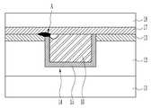
도 1은 종래 반도체 소자의 구리 배선 형성 방법을 설명하기 위한 소자의 단면도이다.1 is a cross-sectional view of a device for explaining a method of forming a copper wiring of a conventional semiconductor device.
기판(11) 상에 제 1 층간 절연막(12) 및 연마 정지층(13)을 형성하고, 다마신 기법으로 연마 정지층(13) 및 제 1 층간 절연막(12)을 식각하여 다마신 패턴(14)을 형성한다.The first
다마신 패턴(14)을 포함한 연마 정지층(13) 표면을 따라 구리 확산 방지 도전막(15)을 형성하고, 다마신 패턴(14)이 충분히 매립되도록 구리층을 형성한다. 화학적 기계적 연마 공정을 연마 정지층(13)이 노출될 때까지 실시하여 다마신 패턴(14) 내에 구리 배선(16)을 형성한다. 이후, 구리 배선(16)을 포함한 전체 구조 상에 구리 확산 방지 절연막(17) 및 제 2 층간 절연막(18)을 형성한다.A copper diffusion preventing
상기한 종래 방법은 구리 배선(16)으로부터 구리 원자가 외부로 확산 되는 것을 방지하기 위하여 구리 확산 방지 도전막(15)과 구리 확산 방지 절연막(17)으 로 구리 배선(16)을 밀봉하고 있다. 그런데, 종래 방법에 따라 형성된 구리 배선(16)을 갖는 소자는 구리 원자의 이동(Electro-migration and stress migration)에 의해 발생하는 대부분의 배선 신뢰성 불량이, 지시 부호 "A"에 나타낸 바와 같이, 구리 확산 방지 절연막(17)과 구리 확산 방지 도전막(15) 사이의 계면에서 일어나고 있다. 이러한 현상은 구리 확산 방지 절연막(17)과 하부층(13, 15 및 16)과의 계면 접합성 부족에 기인한다.
In the conventional method described above, the
따라서, 본 발명은 구리 확산 방지 절연막과 그 하부층과의 계면 접합성을 증대시켜 구리 배선의 구리 원자 이동을 방지하여 소자의 전기적 특성 및 신뢰성을 향상시킬 수 있는 반도체 소자의 구리 배선 형성 방법을 제공함에 그 목적이 있다.
Accordingly, the present invention provides a method for forming a copper wiring of a semiconductor device that can improve the electrical properties and reliability of the device by preventing the copper atom movement of the copper wiring by increasing the interfacial bonding between the copper diffusion preventing insulating film and the lower layer thereof. There is a purpose.
이러한 목적을 달성하기 위한 본 발명의 실시예에 따른 반도체 소자의 구리 배선 형성 방법은 기판 상에 제 1 층간 절연막 및 연마 정지층을 형성하는 단계; 상기 연마 정지층 및 제 1 층간 절연막을 식각하여 다마신 패턴을 형성하는 단계; 상기 다마신 패턴을 포함한 상기 연마 정지층 상에 구리 확산 방지 도전막 및 구리층을 형성하는 단계; 상기 다마신 패턴 내에 구리 배선을 형성하는 단계; 상기 구리 배선을 포함한 전체 구조의 표면에 금속 원소 도핑층을 형성하는 단계; 및 상기 금속 원소 도핑층이 형성된 전체 구조 상부에 구리 확산 방지 절연막 및 제 2 층간 절연막을 형성하고, 이들 절연막 증착시의 열에 의해 상기 구리 배선과 상기 구리 확산 방지 절연막 계면에서는 구리 합금층 및 산화금속층이 형성되고, 상기 구리 배선 주변의 층들과 상기 구리 확산 방지 절연막 계면에는 산화금속층이 형성되는 단계를 포함한다.According to another aspect of the present invention, there is provided a method of forming a copper wiring of a semiconductor device, the method including: forming a first interlayer insulating film and a polishing stop layer on a substrate; Etching the polishing stop layer and the first interlayer insulating layer to form a damascene pattern; Forming a copper diffusion preventing conductive film and a copper layer on the polishing stop layer including the damascene pattern; Forming a copper wiring in the damascene pattern; Forming a metal element doping layer on the surface of the entire structure including the copper wiring; And forming a copper diffusion preventing insulating film and a second interlayer insulating film over the entire structure on which the metal element doping layer is formed, and the copper alloy layer and the metal oxide layer are formed at the interface between the copper wiring and the copper diffusion preventing insulating film by heat during deposition of these insulating films. And a metal oxide layer is formed at an interface between the copper wiring and the copper diffusion barrier insulating layer.
상기에서, 상기 금속 원소 도핑층은 임플랜테이션 방법이나 플라즈마 도핑 방법으로 특정 금속 원소를 도핑시켜 형성하되, 상기 구리 합금층의 두께가 50 ~ 500 Å으로 형성되도록 그 깊이와 농도를 조절하여 형성하며, 상기 특정 금속 원소는 Mg, Cd, Be, Sn, Pd 와 같은 금속 원소이다.
In the above, the metal element doping layer is formed by doping a specific metal element by an implantation method or a plasma doping method, and is formed by adjusting the depth and concentration so that the thickness of the copper alloy layer is formed to 50 ~ 500Å, The specific metal element is a metal element such as Mg, Cd, Be, Sn, Pd.
이하, 첨부된 도면을 참조하여 본 발명의 바람직한 실시예를 설명함으로써, 본 발명을 상세하게 설명한다. 그러나, 본 발명은 이하에서 개시되는 실시예에 한정되는 것이 아니라 서로 다른 다양한 형태로 구현될 것이며, 단지 본 실시예는 본 발명의 개시가 완전하도록 하며, 통상의 지식을 가진 자에게 발명의 범주를 완전하게 알려주기 위해 제공되는 것이다.
Hereinafter, exemplary embodiments of the present invention will be described in detail with reference to the accompanying drawings. However, the present invention is not limited to the embodiments disclosed below, but may be implemented in various forms, and only the present embodiments are intended to complete the disclosure of the present invention and to those skilled in the art. It is provided for complete information.
도 2a 내지 2c는 본 발명의 실시예에 따른 반도체 소자의 구리 배선 형성 방법을 설명하기 위한 소자의 단면도이다.2A to 2C are cross-sectional views of devices for describing a method of forming copper wirings of a semiconductor device according to an exemplary embodiment of the present invention.
도 2a를 참조하면, 기판(21) 상에 제 1 층간 절연막(22) 및 연마 정지층(23)을 형성하고, 다마신 기법으로 연마 정지층(23) 및 제 1 층간 절연막(22)을 식각하여 다마신 패턴(24)을 형성한다. 다마신 패턴(24)을 포함한 연마 정지층(23) 표면 을 따라 구리 확산 방지 도전막(25)을 형성하고, 다마신 패턴(24)이 충분히 매립되도록 구리층을 형성한다. 화학적 기계적 연마 공정을 연마 정지층(23)이 노출되는 시점까지 실시하여 다마신 패턴(24) 내에 구리 배선(26)을 형성한다. 구리 배선(26)을 포함한 제 1 층간 절연막(22)의 표면에 특정 금속 원소를 도핑시켜 금속 원소 도핑층(200)을 형성한다.Referring to FIG. 2A, the first
상기에서, 제 1 층간 절연막(22)은 배선과 배선 사이의 기생 캐패시터로 인한 문제를 해결하기 위해 저유전율을 갖는 물질로 형성하는데, 예를 들어, 유전 상수값이 1.5 내지 4.5 대역의 SiO2 계열에 H, F, C, CH3 등이 부분적으로 결합되어 있는 물질이나, C-H를 기본 구조로 하는 SiLKTM제품, FlareTM제품 등의 유기 물질(organic material)이나, 이들 물질의 유전 상수값을 낮추기 위해 이들 물질의 기공도(porosity)를 증가시킨 다공성(porous) 물질로 형성한다.In the above, the first
연마 정지층(23)은 탄소를 함유하지 않은 산화물로 형성하거나, 구리 확산 방지 특성을 가지도록 화학기상증착법(CVD)으로 질소를 함유한 실리콘 질화물 및 실리콘 질화 산화물 또는 탄소를 함유한 실리콘 카바이드 계열의 물질로 형성한다.The
구리 확산 방지 도전막(25)은 ionized PVD TiN, CVD TiN, MOCVD TiN, ionized PVD Ta, ionized PVD TaN, CVD Ta, CVD TaN, CVD WN 중 어느 하나로 형성한다.The copper diffusion preventing
금속 원소 도핑층(200)은 임플랜테이션 방법이나 플라즈마 도핑 방법으로 특정 금속 원소를 일정 농도 및 일정 깊이로 도핑시켜 형성한다. 특정 금속 원소는 일정 온도에서 구리에 일정 농도 용해되어 합금을 형성하고, 그레인 바운더리(grain boundary)에 석출되어 구리 원자의 이동을 억제하는 특성이 있으며, 미량의 산소와 반응하여 치밀한 막질의 산화금속물을 형성하는 특성이 있는 Mg, Cd, Be, Sn, Pd 와 같은 금속 원소이다. 금속 원소 도핑층(200)은 특정 금속 원소로 인한 구리 배선의 비저항 증가를 최소화 하면서 계면 접합성을 최대화 할 수 있도록 조건을 설정하여 형성하는데, 이후에 형성될 구리 합금층의 두께가 500 Å 이하, 바람직하게는 50 ~ 500 Å, 더욱 바람직하게는 100 ~ 400 Å으로 형성되도록 깊이와 농도를 조절하여 형성한다. 이때, 도핑하는 특정 금속 원소의 농도는 10%를 넘지 않도록, 바람직하게는 1 ~ 10%, 더욱 바람직하게는 3 ~ 8%로 한다.The metal element doped
도 2b를 참조하면, 금속 원소 도핑층(200)이 형성된 전체 구조 상부에 구리 확산 방지 절연막(27)을 형성한다.Referring to FIG. 2B, a copper diffusion
상기에서, 구리 확산 방지 절연막(27)은 실리콘 질화물(SiNx), 실리콘 카바이드(SiCx) 및 실리콘 질화 카바이드(SiCN)중 적어도 어느 하나의 물질을 사용하여 단층 또는 다층으로 300 Å 이상의 두께로 형성하는데, 이들 물질 모두에는 미량의 산소를 함유하도록 한다.In the above, the copper diffusion
한편, 구리 확산 방지 절연막(27)을 형성하기 전에 구리 배선(26)을 안정화 시키면서 구리 배선(26) 표면에 생성되는 구리 산화층(도시 않음)을 제거하기 위하여 플라즈마 처리를 실시한다. 플라즈마 처리는 금속 원소 도핑층(200)을 형성하기 전에 실시하거나 금속 원소 도핑층(200)을 형성한 후 구리 확산 방지 절연막(27)을 형성하기 바로 전에 실시할 수 있으며, 금속 원소 도핑층(200)을 형성하기 전후 모 두 실시할 수도 있으며, 금속 원소 도핑층(200)을 형성하기 위한 특정 금속 원소 도핑 중에 인-시튜(in-situ)로 실시할 수도 있다. 이러한 플라즈마 처리는 질소와 수소를 함유한 혼합가스 또는 암모니아 계열 가스를 사용하여 100 ~ 350℃의 온도 범위에서 실시한다.On the other hand, plasma treatment is performed to remove the copper oxide layer (not shown) generated on the surface of the
도 2c를 참조하면, 구리 확산 방지 절연막(27)을 포함한 전체 구조 상에 제 2 층간 절연막(28)을 형성한다. 금속 원소 도핑층(200)의 특정 금속 원소가 주위의 다른 원소와 반응하도록 열처리 공정을 실시하고, 이로 인하여 구리 배선(26)과 구리 확산 방지 절연막(27) 계면에서는 구리 합금층(210) 및 산화금속층(220)이 적층으로 형성되고, 연마 정지층(23)과 구리 확산 방지 절연막(27) 계면에서는 산화금속층(220)이 형성된다. 또한 구리 확산 방지 도전막(25)과 구리 확산 방지 절연막(27) 계면에도 산화금속층(220)이 형성된다.Referring to FIG. 2C, a second
상기에서, 제 2 층간 절연막(28)은 다층 금속 배선 구조일 경우에는 전술한 제 1 층간 절연막(22)과 같이 배선과 배선 사이의 기생 캐패시터로 인한 문제를 해결하기 위해 저유전율을 갖는 물질로 형성하는 것이 바람직하지만, 단층 금속 배선 구조일 경우에는 통상적으로 반도체 소자의 층간 절연막으로 적용되는 다른 절연물로도 형성할 수 있다.In the above, the second
열처리 공정은 100 ~ 500 ℃의 온도 범위에서 1분 이상, 바람직하게는 1 ~ 5분 동안 실시한다.The heat treatment process is carried out for at least 1 minute, preferably 1 to 5 minutes in the temperature range of 100 ~ 500 ℃.
구리 합금층(210)은 금속 원소 도핑층(200)의 특정 금속 원소가 열처리 공정 동안에 구리 배선(26)의 구리 원소에 용해되어 형성된다. 구리 배선(26) 윗 부분 및 구리 배선(26) 주변의 층들(23 및 25)의 윗 부분에 형성되는 산화금속층(220)은 구리 확산 방지 절연막(27)에 함유된 미량의 산소와 금속 원소 도핑층(200)의 특정 금속 원소가 결합하여 치밀한 막질로 형성된다.
The
상술한 바와 같이, 본 발명은 구리 배선과 구리 확산 방지 절연막 계면에 구리 합금층 및 산화금속층이 적층으로 형성되고, 구리 배선 주변의 층들과 구리 확산 방지 절연막 계면에 산화금속층이 형성되어 구리 확산 방지 절연막의 계면 접합성이 증대되므로, 배선의 신뢰성 향상으로 인한 소자의 전기적 특성 및 수율을 향상시킬 수 있다.As described above, according to the present invention, a copper alloy layer and a metal oxide layer are formed on the interface between the copper wiring and the copper diffusion preventing insulating film, and a metal oxide layer is formed on the interfaces between the copper wiring and the copper diffusion preventing insulating film to prevent the copper diffusion insulating film. Since the interfacial bonding property of is increased, it is possible to improve the electrical characteristics and the yield of the device due to the improved reliability of the wiring.
Claims (8)
Translated fromKoreanPriority Applications (3)
| Application Number | Priority Date | Filing Date | Title |
|---|---|---|---|
| KR1020030046295AKR100546209B1 (en) | 2003-07-09 | 2003-07-09 | Copper wiring formation method of semiconductor device |
| JP2003389232AJP4482313B2 (en) | 2003-07-09 | 2003-11-19 | Method for forming copper wiring of semiconductor element |
| US10/720,849US7087524B2 (en) | 2003-07-09 | 2003-11-24 | Method of forming copper wiring in semiconductor device |
Applications Claiming Priority (1)
| Application Number | Priority Date | Filing Date | Title |
|---|---|---|---|
| KR1020030046295AKR100546209B1 (en) | 2003-07-09 | 2003-07-09 | Copper wiring formation method of semiconductor device |
Publications (2)
| Publication Number | Publication Date |
|---|---|
| KR20050006472A KR20050006472A (en) | 2005-01-17 |
| KR100546209B1true KR100546209B1 (en) | 2006-01-24 |
Family
ID=33562948
Family Applications (1)
| Application Number | Title | Priority Date | Filing Date |
|---|---|---|---|
| KR1020030046295AExpired - LifetimeKR100546209B1 (en) | 2003-07-09 | 2003-07-09 | Copper wiring formation method of semiconductor device |
Country Status (3)
| Country | Link |
|---|---|
| US (1) | US7087524B2 (en) |
| JP (1) | JP4482313B2 (en) |
| KR (1) | KR100546209B1 (en) |
Families Citing this family (14)
| Publication number | Priority date | Publication date | Assignee | Title |
|---|---|---|---|---|
| US7402519B2 (en)* | 2005-06-03 | 2008-07-22 | Intel Corporation | Interconnects having sealing structures to enable selective metal capping layers |
| JP2007180420A (en)* | 2005-12-28 | 2007-07-12 | Fujitsu Ltd | Manufacturing method of semiconductor device and manufacturing method of magnetic head |
| WO2008074672A1 (en)* | 2006-12-20 | 2008-06-26 | Nxp B.V. | Improving adhesion of diffusion barrier on cu containing interconnect element |
| US8764961B2 (en)* | 2008-01-15 | 2014-07-01 | Applied Materials, Inc. | Cu surface plasma treatment to improve gapfill window |
| DE102008007001B4 (en)* | 2008-01-31 | 2016-09-22 | Globalfoundries Dresden Module One Limited Liability Company & Co. Kg | Increasing the resistance to electromigration in a connection structure of a semiconductor device by forming an alloy |
| US8043976B2 (en)* | 2008-03-24 | 2011-10-25 | Air Products And Chemicals, Inc. | Adhesion to copper and copper electromigration resistance |
| JP2010045161A (en)* | 2008-08-12 | 2010-02-25 | Toshiba Corp | Semiconductor device and its manufacturing method |
| US8358007B2 (en)* | 2009-06-11 | 2013-01-22 | Globalfoundries Singapore Pte. Ltd. | Integrated circuit system employing low-k dielectrics and method of manufacture thereof |
| KR102420689B1 (en) | 2010-02-26 | 2022-07-15 | 가부시키가이샤 한도오따이 에네루기 켄큐쇼 | Semiconductor device |
| KR20130045418A (en) | 2010-04-23 | 2013-05-03 | 가부시키가이샤 한도오따이 에네루기 켄큐쇼 | Manufacturing method of semiconductor device |
| CN102903666B (en)* | 2011-07-25 | 2015-04-01 | 中芯国际集成电路制造(上海)有限公司 | Manufacturing method of semiconductor device |
| US9425092B2 (en)* | 2013-03-15 | 2016-08-23 | Applied Materials, Inc. | Methods for producing interconnects in semiconductor devices |
| US20140273436A1 (en)* | 2013-03-15 | 2014-09-18 | Globalfoundries Inc. | Methods of forming barrier layers for conductive copper structures |
| US10756008B2 (en)* | 2016-03-25 | 2020-08-25 | Hitachi Chemical Company, Ltd. | Organic interposer and method for manufacturing organic interposer |
Family Cites Families (3)
| Publication number | Priority date | Publication date | Assignee | Title |
|---|---|---|---|---|
| JP3737366B2 (en)* | 1999-03-19 | 2006-01-18 | 東京エレクトロン株式会社 | Semiconductor device and manufacturing method thereof |
| US6800554B2 (en)* | 2000-12-18 | 2004-10-05 | Intel Corporation | Copper alloys for interconnections having improved electromigration characteristics and methods of making same |
| US6815331B2 (en)* | 2001-05-17 | 2004-11-09 | Samsung Electronics Co., Ltd. | Method for forming metal wiring layer of semiconductor device |
- 2003
- 2003-07-09KRKR1020030046295Apatent/KR100546209B1/ennot_activeExpired - Lifetime
- 2003-11-19JPJP2003389232Apatent/JP4482313B2/ennot_activeExpired - Lifetime
- 2003-11-24USUS10/720,849patent/US7087524B2/ennot_activeExpired - Lifetime
Also Published As
| Publication number | Publication date |
|---|---|
| JP4482313B2 (en) | 2010-06-16 |
| US20050009331A1 (en) | 2005-01-13 |
| US7087524B2 (en) | 2006-08-08 |
| JP2005033160A (en) | 2005-02-03 |
| KR20050006472A (en) | 2005-01-17 |
Similar Documents
| Publication | Publication Date | Title |
|---|---|---|
| US6130161A (en) | Method of forming copper interconnections with enhanced electromigration resistance and reduced defect sensitivity | |
| US6972253B2 (en) | Method for forming dielectric barrier layer in damascene structure | |
| US7507666B2 (en) | Manufacture method for semiconductor device having concave portions filled with conductor containing Cu as its main composition | |
| KR100546209B1 (en) | Copper wiring formation method of semiconductor device | |
| US8378488B2 (en) | Semiconductor device and method of manufacturing the same | |
| US6511908B2 (en) | Method of manufacturing a dual damascene structure using boron nitride as trench etching stop film | |
| JP4676350B2 (en) | Semiconductor device and manufacturing method thereof | |
| JP4638140B2 (en) | Method for forming copper wiring of semiconductor element | |
| US7247565B2 (en) | Methods for fabricating a copper interconnect | |
| KR100924556B1 (en) | Metal wiring of semiconductor device and method of forming the same | |
| KR100973277B1 (en) | Metal wiring of semiconductor device and method of forming the same | |
| KR100546940B1 (en) | Copper wiring formation method of semiconductor device | |
| KR100744669B1 (en) | Method of forming metal wire using dama copper | |
| KR100525906B1 (en) | Method of forming a copper wiring in a semiconductor device | |
| KR20050006468A (en) | Method of forming copper wiring in semiconductor device | |
| KR100935193B1 (en) | Metal wiring of semiconductor device and forming method thereof | |
| KR100784106B1 (en) | Metal wiring formation method of semiconductor device | |
| KR101029107B1 (en) | Metal wiring of semiconductor device and method of forming the same | |
| KR100567539B1 (en) | Metal wiring formation method of semiconductor device | |
| KR101029105B1 (en) | Metal wiring of semiconductor device and method of forming the same | |
| KR100924557B1 (en) | Metal wiring of semiconductor device and method of forming the same | |
| KR20040057547A (en) | Method for forming copper wire in a semiconductor device | |
| JP2007005628A (en) | Wiring structure and manufacturing method thereof | |
| KR20050009932A (en) | Method of forming copper wiring in semiconductor device | |
| KR20050009621A (en) | Method of forming copper wiring in semiconductor device |
Legal Events
| Date | Code | Title | Description |
|---|---|---|---|
| A201 | Request for examination | ||
| PA0109 | Patent application | Patent event code:PA01091R01D Comment text:Patent Application Patent event date:20030709 | |
| PA0201 | Request for examination | ||
| N231 | Notification of change of applicant | ||
| PN2301 | Change of applicant | Patent event date:20041006 Comment text:Notification of Change of Applicant Patent event code:PN23011R01D | |
| PG1501 | Laying open of application | ||
| E902 | Notification of reason for refusal | ||
| PE0902 | Notice of grounds for rejection | Comment text:Notification of reason for refusal Patent event date:20050711 Patent event code:PE09021S01D | |
| E701 | Decision to grant or registration of patent right | ||
| PE0701 | Decision of registration | Patent event code:PE07011S01D Comment text:Decision to Grant Registration Patent event date:20060111 | |
| GRNT | Written decision to grant | ||
| PR0701 | Registration of establishment | Comment text:Registration of Establishment Patent event date:20060118 Patent event code:PR07011E01D | |
| PR1002 | Payment of registration fee | Payment date:20060117 End annual number:3 Start annual number:1 | |
| PG1601 | Publication of registration | ||
| PR1001 | Payment of annual fee | Payment date:20090102 Start annual number:4 End annual number:4 | |
| PR1001 | Payment of annual fee | Payment date:20091217 Start annual number:5 End annual number:5 | |
| PR1001 | Payment of annual fee | Payment date:20101217 Start annual number:6 End annual number:6 | |
| PR1001 | Payment of annual fee | Payment date:20111222 Start annual number:7 End annual number:7 | |
| FPAY | Annual fee payment | Payment date:20121210 Year of fee payment:8 | |
| PR1001 | Payment of annual fee | Payment date:20121210 Start annual number:8 End annual number:8 | |
| FPAY | Annual fee payment | Payment date:20131217 Year of fee payment:9 | |
| PR1001 | Payment of annual fee | Payment date:20131217 Start annual number:9 End annual number:9 | |
| FPAY | Annual fee payment | Payment date:20141222 Year of fee payment:10 | |
| PR1001 | Payment of annual fee | Payment date:20141222 Start annual number:10 End annual number:10 | |
| FPAY | Annual fee payment | Payment date:20151217 Year of fee payment:11 | |
| PR1001 | Payment of annual fee | Payment date:20151217 Start annual number:11 End annual number:11 | |
| FPAY | Annual fee payment | Payment date:20161220 Year of fee payment:12 | |
| PR1001 | Payment of annual fee | Payment date:20161220 Start annual number:12 End annual number:12 | |
| FPAY | Annual fee payment | Payment date:20171218 Year of fee payment:13 | |
| PR1001 | Payment of annual fee | Payment date:20171218 Start annual number:13 End annual number:13 | |
| FPAY | Annual fee payment | Payment date:20191226 Year of fee payment:15 | |
| PR1001 | Payment of annual fee | Payment date:20191226 Start annual number:15 End annual number:15 | |
| PR1001 | Payment of annual fee | Payment date:20210113 Start annual number:16 End annual number:16 | |
| PR1001 | Payment of annual fee | Payment date:20220118 Start annual number:17 End annual number:17 | |
| PR1001 | Payment of annual fee | Payment date:20230118 Start annual number:18 End annual number:18 | |
| PC1801 | Expiration of term | Termination date:20240109 Termination category:Expiration of duration |