KR100543176B1 - Printing Head Device for Nano Patterning - Google Patents
Printing Head Device for Nano PatterningDownload PDFInfo
- Publication number
- KR100543176B1 KR100543176B1KR1020030078338AKR20030078338AKR100543176B1KR 100543176 B1KR100543176 B1KR 100543176B1KR 1020030078338 AKR1020030078338 AKR 1020030078338AKR 20030078338 AKR20030078338 AKR 20030078338AKR 100543176 B1KR100543176 B1KR 100543176B1
- Authority
- KR
- South Korea
- Prior art keywords
- patterning
- injection
- shadow mask
- printing head
- actuator
- Prior art date
- Legal status (The legal status is an assumption and is not a legal conclusion. Google has not performed a legal analysis and makes no representation as to the accuracy of the status listed.)
- Expired - Lifetime
Links
Images


Classifications
- C—CHEMISTRY; METALLURGY
- C23—COATING METALLIC MATERIAL; COATING MATERIAL WITH METALLIC MATERIAL; CHEMICAL SURFACE TREATMENT; DIFFUSION TREATMENT OF METALLIC MATERIAL; COATING BY VACUUM EVAPORATION, BY SPUTTERING, BY ION IMPLANTATION OR BY CHEMICAL VAPOUR DEPOSITION, IN GENERAL; INHIBITING CORROSION OF METALLIC MATERIAL OR INCRUSTATION IN GENERAL
- C23C—COATING METALLIC MATERIAL; COATING MATERIAL WITH METALLIC MATERIAL; SURFACE TREATMENT OF METALLIC MATERIAL BY DIFFUSION INTO THE SURFACE, BY CHEMICAL CONVERSION OR SUBSTITUTION; COATING BY VACUUM EVAPORATION, BY SPUTTERING, BY ION IMPLANTATION OR BY CHEMICAL VAPOUR DEPOSITION, IN GENERAL
- C23C16/00—Chemical coating by decomposition of gaseous compounds, without leaving reaction products of surface material in the coating, i.e. chemical vapour deposition [CVD] processes
- B—PERFORMING OPERATIONS; TRANSPORTING
- B41—PRINTING; LINING MACHINES; TYPEWRITERS; STAMPS
- B41J—TYPEWRITERS; SELECTIVE PRINTING MECHANISMS, i.e. MECHANISMS PRINTING OTHERWISE THAN FROM A FORME; CORRECTION OF TYPOGRAPHICAL ERRORS
- B41J2/00—Typewriters or selective printing mechanisms characterised by the printing or marking process for which they are designed
- B41J2/005—Typewriters or selective printing mechanisms characterised by the printing or marking process for which they are designed characterised by bringing liquid or particles selectively into contact with a printing material
- B41J2/01—Ink jet
- B41J2/07—Ink jet characterised by jet control
- B—PERFORMING OPERATIONS; TRANSPORTING
- B01—PHYSICAL OR CHEMICAL PROCESSES OR APPARATUS IN GENERAL
- B01L—CHEMICAL OR PHYSICAL LABORATORY APPARATUS FOR GENERAL USE
- B01L3/00—Containers or dishes for laboratory use, e.g. laboratory glassware; Droppers
- B01L3/02—Burettes; Pipettes
- B01L3/0241—Drop counters; Drop formers
- B01L3/0268—Drop counters; Drop formers using pulse dispensing or spraying, eg. inkjet type, piezo actuated ejection of droplets from capillaries
- B—PERFORMING OPERATIONS; TRANSPORTING
- B41—PRINTING; LINING MACHINES; TYPEWRITERS; STAMPS
- B41J—TYPEWRITERS; SELECTIVE PRINTING MECHANISMS, i.e. MECHANISMS PRINTING OTHERWISE THAN FROM A FORME; CORRECTION OF TYPOGRAPHICAL ERRORS
- B41J2/00—Typewriters or selective printing mechanisms characterised by the printing or marking process for which they are designed
- B41J2/005—Typewriters or selective printing mechanisms characterised by the printing or marking process for which they are designed characterised by bringing liquid or particles selectively into contact with a printing material
- B41J2/01—Ink jet
- B41J2/135—Nozzles
- B41J2/14—Structure thereof only for on-demand ink jet heads
- B—PERFORMING OPERATIONS; TRANSPORTING
- B82—NANOTECHNOLOGY
- B82Y—SPECIFIC USES OR APPLICATIONS OF NANOSTRUCTURES; MEASUREMENT OR ANALYSIS OF NANOSTRUCTURES; MANUFACTURE OR TREATMENT OF NANOSTRUCTURES
- B82Y30/00—Nanotechnology for materials or surface science, e.g. nanocomposites
- B—PERFORMING OPERATIONS; TRANSPORTING
- B01—PHYSICAL OR CHEMICAL PROCESSES OR APPARATUS IN GENERAL
- B01L—CHEMICAL OR PHYSICAL LABORATORY APPARATUS FOR GENERAL USE
- B01L2400/00—Moving or stopping fluids
- B01L2400/02—Drop detachment mechanisms of single droplets from nozzles or pins
- B01L2400/027—Drop detachment mechanisms of single droplets from nozzles or pins electrostatic forces between substrate and tip
- B—PERFORMING OPERATIONS; TRANSPORTING
- B01—PHYSICAL OR CHEMICAL PROCESSES OR APPARATUS IN GENERAL
- B01L—CHEMICAL OR PHYSICAL LABORATORY APPARATUS FOR GENERAL USE
- B01L2400/00—Moving or stopping fluids
- B01L2400/04—Moving fluids with specific forces or mechanical means
- B01L2400/0403—Moving fluids with specific forces or mechanical means specific forces
- B01L2400/0433—Moving fluids with specific forces or mechanical means specific forces vibrational forces
- B01L2400/0439—Moving fluids with specific forces or mechanical means specific forces vibrational forces ultrasonic vibrations, vibrating piezo elements
- B—PERFORMING OPERATIONS; TRANSPORTING
- B33—ADDITIVE MANUFACTURING TECHNOLOGY
- B33Y—ADDITIVE MANUFACTURING, i.e. MANUFACTURING OF THREE-DIMENSIONAL [3-D] OBJECTS BY ADDITIVE DEPOSITION, ADDITIVE AGGLOMERATION OR ADDITIVE LAYERING, e.g. BY 3-D PRINTING, STEREOLITHOGRAPHY OR SELECTIVE LASER SINTERING
- B33Y30/00—Apparatus for additive manufacturing; Details thereof or accessories therefor
- B—PERFORMING OPERATIONS; TRANSPORTING
- B82—NANOTECHNOLOGY
- B82Y—SPECIFIC USES OR APPLICATIONS OF NANOSTRUCTURES; MEASUREMENT OR ANALYSIS OF NANOSTRUCTURES; MANUFACTURE OR TREATMENT OF NANOSTRUCTURES
- B82Y40/00—Manufacture or treatment of nanostructures
Landscapes
- Chemical & Material Sciences (AREA)
- Engineering & Computer Science (AREA)
- Nanotechnology (AREA)
- Chemical Kinetics & Catalysis (AREA)
- Materials Engineering (AREA)
- General Physics & Mathematics (AREA)
- Composite Materials (AREA)
- Condensed Matter Physics & Semiconductors (AREA)
- Health & Medical Sciences (AREA)
- Physics & Mathematics (AREA)
- Crystallography & Structural Chemistry (AREA)
- Clinical Laboratory Science (AREA)
- General Chemical & Material Sciences (AREA)
- Mechanical Engineering (AREA)
- Metallurgy (AREA)
- Organic Chemistry (AREA)
- Coating Apparatus (AREA)
Abstract
Translated fromKoreanDescription
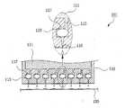
Translated fromKorean도 1은 종래 나노 패터닝용 프린팅헤드 장치의 단면도,1 is a cross-sectional view of a conventional printing head device for nano patterning,
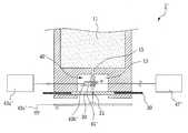
도 2는 본 발명에 따른 패터닝용 프린팅헤드 장치의 간략한 단면도,2 is a simplified cross-sectional view of a printing head device for patterning according to the present invention;
도 3는 도 2의 쉐도우마스크 설치영역의 사시도,3 is a perspective view of the shadow mask installation area of FIG.
도 4는 본 발명의 다른 실시예에 따른 패터닝용 프린팅헤드 장치의 간략한 단면도.4 is a simplified cross-sectional view of a printing head device for patterning according to another embodiment of the present invention.
* 도면의 주요 부분에 대한 부호의 설명* Explanation of symbols for the main parts of the drawings
10 : 카트리지 11 : 매니폴더 10: cartridge 11: manifold
13 : 분사챔버 20 : 쉐도우마스크 13: injection chamber 20: shadow mask
21 : 분사홀 30 : 엑츄에이터 21: injection hole 30: actuator
40 : 분사유도유닛 41 : 모세관 40: injection guide unit 41: capillary tube
43b : 전원공급전극 43c : 대향전극43b:
45 : 가스공급부 45: gas supply unit
본 발명은, 나노 패터닝용 프린팅헤드 장치에 관한 것으로서, 보다 상세하게 는 쉐도우마스크의 구조와 분사구조를 개선하여, 패터닝의 정밀도가 향상되고, 초미세 나노 패터닝과 임의 형상의 패터닝이 가능한 나노 패터닝용 프린팅헤드 장치를 제공하는 것이다.The present invention relates to a printing head device for nano-patterning, and more particularly, to improve the shadow mask structure and the spraying structure, thereby improving the precision of patterning, and for nano-patterning capable of ultra-fine nano patterning and patterning of arbitrary shapes. It is to provide a printing head device.
반도체 등의 나노 기술분야에서의 집적회로 및 미세 조형물의 패터닝 방법 중 대표적인 예로는 식각(Lithography) 및 에칭(Etching)을 들 수 있다.Representative examples of the patterning method of integrated circuits and micro-structures in the nanotechnology field such as semiconductors include etching and etching.
그러나, 이러한 식각(Lithography) 및 에칭(Etching)을 이용한 패터닝 방법은 공정시간이 오래 걸리고, 패터닝 과정에서의 이물질 유입에 의한 오염, 재질 적용의 한계 및 복잡한 공정에 의한 정밀도 저하의 문제점을 가지고 있었다.However, such a patterning method using lithography and etching takes a long process time, and has problems such as contamination due to inflow of foreign substances in the patterning process, limitation of material application, and deterioration of precision due to a complicated process.
이러한 문제점을 개선하기 위해 잉크젯 프린팅 분야에서 사용되는 프린팅헤드 장치를 이용하여 반도체 집적회로 및 미세 조형물 등을 패터닝 하는 기술이 개시된 바 있다.In order to improve such a problem, a technology for patterning semiconductor integrated circuits and fine sculptures using a printing head device used in the field of inkjet printing has been disclosed.
도 1은 종래 패터닝용 프린팅헤드 장치의 간략한 단면도이다. 이 도면에 도시된 바와 같이, 종래 패터닝용 프린팅헤드 장치(101)는 카트리지(110)내에 프린팅 물질(초미세 입자 또는 접착 용액 또는 폴리머 등)를 수용하는 매니폴더(111)가 형성되어 있고, 매니폴더(111) 하부에 각각 독립된 공간의 분사챔버(113)가 다수 형성되어 있다.1 is a simplified cross-sectional view of a conventional printing head device for patterning. As shown in this figure, the conventional
각 분사챔버(113)는 매니폴더(111)와 액체공급로(115)에 의해 연결되어 있으며, 각 분사챔버(113)의 하부에는 프린팅물질이 외부로 분사될 수 있도록 노즐(116)이 각각 형성되어 있다. 이때, 각 분사챔버(113)의 상측에는 분사챔버(113) 내에 버블을 형성하는 히터(117)(또는 피에조-PZT)가 설치되어 있다. 이 히터(117)(또는 PZT)의 구동에 의해 분사챔버(113) 내에 버블이 형성되면 분사챔버(113)내에 수용되어 있던 프린팅물질이 버블의 형성 압력에 의해 노즐(116)을 통해 외부로 분사된다.Each
이 프린팅헤드 장치(101)는 도시않은 제어부의 제어동작에 의해서 미리 설정된 패터닝 좌표에 대응하는 위치로 이동하면서 패터닝영역에 프린팅물질을 분사하여 샘플홀더(120)에 반도체 집적회로 또는 미세 조형물 등을 패터닝한다.The
그런데, 이러한 종래 패터닝용 프린팅 장치는 버블의 형성 압력에 의해 노즐을 통해 프린팅물질이 분사될 때, 노즐경에 발생되는 표면장력을 고려해서 노즐 직경을 비교적 크게 형성해야 하기 때문에, 초미세 집적회로나 조형물의 패터닝이 불가능하다는 문제점이 있다.However, such a conventional printing apparatus for patterning has to form a nozzle diameter relatively large in consideration of the surface tension generated in the nozzle diameter when the printing material is injected through the nozzle by the pressure of bubble formation. There is a problem that the patterning of the sculpture is impossible.
또한, 프린팅물질의 패터닝영역이 프린팅헤드의 동작영역에 국한되기 때문에 초미세 패터닝과 임의형상 패터닝이 어렵다는 문제점이 있다.In addition, since the patterning area of the printing material is limited to the operating area of the printing head, there is a problem in that ultrafine patterning and arbitrary shape patterning are difficult.
따라서, 본 발명의 목적은, 패터닝의 정밀도가 향상되고, 초미세 패터닝과 임의 형상의 패터닝이 가능한 나노 패터닝용 프린팅헤드 장치를 제공하는 것이다.Accordingly, an object of the present invention is to provide a printing head device for nano patterning, in which the precision of patterning is improved, and ultra-fine patterning and arbitrary patterning are possible.
상기 목적은, 본 발명에 따라, 액체상의 프린팅물질을 수용하는 매니폴더와, 상기 매니폴더와 연통되는 분사챔버를 갖는 카트리지와; 상기 카트리지의 분사챔버측 외측에 설치되는 패터닝용 샘플홀더를 갖는 나노 패터닝용 프린팅헤드 장치에 있어서, 상기 분사챔버 외측에 X-Y 평면방향으로 미세 유동 가능하게 설치되며, 100nm이하의 단일의 분사홀을 갖는 쉐도우마스크와; 상기 쉐도우마스크를 미세 유동 시키는 엑츄에이터와; 고전압발생기와, 상기 고전압발생기로부터 전원을 인가받으며 상기 분사챔버 내에 설치되어 양전하를 형성하는 전원공급전극과, 상기 쉐도우마스크를 사이에 두고 상기 샘플홀더에 음전하를 형성하는 대향전극을 가지고 상기 분사챔버로부터 상기 샘플홀더를 향해 유도방전을 형성하는 분사유도유닛과; 미리 입력된 패터닝 데이터에 대응하는 패터닝 위치로 상기 쉐도우마스크의 분사홀이 이동하도록 상기 엑츄에이터의 구동을 제어하는 제어부를 포함하는 것을 특징으로 하는 나노 패터닝용 프린팅헤드 장치에 의하여 달성된다.The object is, according to the present invention, a cartridge having a manifold for receiving a liquid printing material and an injection chamber in communication with the manifold; A nano-patterned printing head device having a patterning sample holder installed outside the ejection chamber side of the cartridge, the nanopatterning printing head device having a single ejection hole of 100 nm or less installed in the XY plane direction outside the ejection chamber. Shadow masks; An actuator for finely flowing the shadow mask; A high voltage generator, a power supply electrode receiving power from the high voltage generator and installed in the injection chamber to form a positive charge, and an opposite electrode forming a negative charge in the sample holder with the shadow mask therebetween from the injection chamber; An injection guide unit for forming an induced discharge toward the sample holder; And a control unit for controlling the driving of the actuator to move the injection hole of the shadow mask to a patterning position corresponding to previously input patterning data.
여기서, 상기 분사유도유닛은 상기 매니폴더와 상기 분사챔버를 연통시키며 상기 전원공급전극이 설치되는 모세관과, 상기 모세관내에 작용가스를 공급하는 가스공급기와, 상기 가스공급기와 상기 모세관을 연결하는 가스공습호스를 갖는 가스공급부를 가지고 상기 전원공급전극으로부터 상기 모세관을 통해 상기 대향전극을 향하는 방전 프라즈마를 형성하는 것이 바람직하다.Here, the injection guide unit is in communication with the manifold and the injection chamber, the capillary tube is provided with the power supply electrode, the gas supply for supplying the working gas in the capillary tube, the gas air connection connecting the gas supply and the capillary tube It is preferred to have a gas supply with a hose to form a discharge plasma from the power supply electrode toward the counter electrode through the capillary.
또는, 상기 분사유도유닛은 상기 전원공급전극과 전기적으로 연결되어 상기 분사챔버내에 설치되는 압전소자와, 상기 압전소자에 고주파를 인가하는 고주파발생기를 갖는 것이 효과적이다.Alternatively, the injection induction unit is effective to have a piezoelectric element electrically connected to the power supply electrode and installed in the injection chamber, and a high frequency generator for applying a high frequency to the piezoelectric element.
그리고, 상기 제어부는 상기 패터닝 데이터에 대응하는 위치로 상기 프린팅 헤드를 1차적으로 위치 이동시키는 한편, 상기 엑츄에이터를 구동시켜 상기 쉐도우마스크를 2차적으로 위치 이동시키는 것이 보다 바람직하다.In addition, the controller may primarily move the printing head to a position corresponding to the patterning data, and drive the actuator to move the shadow mask secondarily.
삭제delete
이하에서는 첨부된 도면을 참고하여 본 발명을 상세히 설명하기로 한다.Hereinafter, with reference to the accompanying drawings will be described in detail the present invention.
도 2는 본 발명에 따른 나노 패터닝용 프린팅헤드 장치의 간략한 단면도이고, 도 3은 도 2의 쉐도우마스크 설치영역의 사시도이다. 이들 도면에 도시된 바와 같이, 본 발명에 따른 패터닝용 프린팅헤드 장치(1)는 프린팅물질을 수용하는 카트리지(10)와, 카트리지(10) 내에 수용된 프린팅물질의 외부 분사를 유도하는 분사유도유닛(40)과, 단일의 분사홀(21)을 가지고 카트리지(10)의 하부에 미세 유동 가능하게 설치되어 프린팅물질의 분사영역을 제어하는 쉐도우마스크(20)와, 쉐도우마스크(20)를 미세 유동시키는 엑츄에이터(30)와, 프린팅헤드 장치(1) 및 엑츄에이터(30)의 구동을 제어하는 제어부(미도시)를 갖는다.Figure 2 is a simplified cross-sectional view of the printing head device for nano patterning according to the present invention, Figure 3 is a perspective view of the shadow mask installation area of FIG. As shown in these drawings, the
카트리지(10)내에는 프린팅물질을 수용하는 매니폴더(11)가 형성되어 있고, 매니폴더(11) 하부에 소정 크기의 단일 공간으로서 분사챔버(13)가 형성되어 있다. 매니폴더(11)에 수용되는 프린팅물질은 패터닝 대상에 따라 반도체 분야에서의 집적회로 패터닝을 위한 액체 공액 폴리머가 수용될 수 있으며, 또는, 급속조형의 3DP(Three Dimensional Printing)분야에서의 분말 접착을 위한 액체바인더 물질 또는, 프린트 분야에서의 프린팅용 잉크 등의 유기체 또는 무기체일 수 있다.In the
분사유도유닛(40)은 ESD(Electrospray Deposition) 방식으로서 매니폴더(11)와 분사챔버(13)를 연통시키는 모세관(41)과, 모세관(41)내에 플라즈마를 형성시키는 플라즈마발생부(43)와, 모세관(41)내에 작용가스를 공급하는 가스공급부(45a)를 포함한다.The
모세관(41)은 매니폴더(11)에 수용된 액상의 프린팅물질을 분사챔버(13)로 공급되도록 하는 공급경로의 역할을 함과 동시에 , 액체상의 프린팅물질이 모세관(41) 내에서 발생되는 플라즈마에 의해 기체상으로 변환되는 공간을 형성한다.The
플라즈마발생부(43)는 모세관(41) 내에 핀형태로 마련되어 외부 전원공급부(43a)와 전기적으로 연결되어 양전하를 형성하는 전원공급전극(43b)과, 쉐도우마스크(20)를 사이에 두고 프린팅물질이 패터닝될 샘플홀더(50)(sample holder)에 접지되어 전원공급전극(43b)에 대향하는 음전하를 형성하는 대향전극(43c)을 갖는다. 즉, 전원공급전극(43b)이 설치된 모세관(41)과 대향전극(43c) 사이에 쉐도우마스크(20)가 위치하게 된다.The
플라즈마발생부(43)는 전원공급전극(43b)으로부터 모세관(41)을 통해 대향전극(43c)을 향하는 방전 프라즈마를 형성함으로써, 작용가스가 공급되는 모세관(41)에서 프린팅물질(약 50nm 이하)로 기화되어 분사챔버(13)를 거쳐 쉐도우마스크(20)의 분사홀(21)을 통해 분사되도록 유도한다.The
가스공급부(45)는 작용가스를 공급하는 가스공급기(45a)와 가스공급기(45a) 로부터 공급되는 작용가스를 모세관(41)으로 안내하는 가스공급호스(45b)로 이루어진다.The
쉐도우마스크(20)에는 비교적 작은 직경의 단일 분사홀(21)이 형성되어 있다. 이 쉐도우마스크(20)는 분사챔버(13) 하부에서 엑츄에이터(30)에 의해 X-Y 평면 방향으로 미세 유동하게 설치된다. 여기서, 분사홀(21)의 직경은 모세관(41)에서 기화된 프린팅물질 입자가 통과할 수 있도록 약 100nm 정도의 직경을 갖는 것이 바람직하다.In the
프린팅물질의 분사영역은 엑츄에이터(30)의 구동에 의해 X-Y평면에서 미세 유동되는 쉐도우마스크(20)의 이동위치에 대응하는 정밀 분사영역에 해당한다.The spraying region of the printing material corresponds to the precision spraying region corresponding to the moving position of the
엑츄에이터(30)는 초미세 부품으로서 제어부(미도시)와 전기적으로 연결되어 제어부(미도시)로부터 전달되는 패터닝 데이터에 근거하여 구동 제어되어 쉐도우마스크(20)를 X-Y 평면상에서 미세 동작시킨다. 이때, 엑츄에이터(30)는 제어부(미도시)에 의해 구동이 제어되는 것으로서, 쉐도우마스크(20)의 이동 방향은 제어부(미도시)에 입력되는 패터닝 데이터에 대응한다.The
제어부(미도시)는 미리 입력된 패터닝 데이터에 근거하여 프린팅헤드(1)의 구동위치를 1차 적으로 제어하고, 엑츄에이터(30)의 구동을 2차 적으로 제어하여 쉐도우마스크(20)를 동작시킴으로써, 프린팅물질의 분사영역 설정한다. 여기서, 프린팅헤드(1)의 구동구조는 일반적인 반도체 제조분야 및 나노기술분야, 잉크젯 프린트 분야에서 적용되는 프린팅헤드(1)의 구동 제어와 동일하게 이루어지는 것이 바람직하다.The controller (not shown) primarily controls the driving position of the
이러한 구성에 의해서, 본 발명에 따른 패터닝용 프린팅헤드(1)에 의한 반도체 집적회로 또는 초미세 조형물의 패터닝 과정을 살펴본다.With this configuration, the patterning process of the semiconductor integrated circuit or the ultra fine sculpture by the
먼저, 도시 하지 않은 제어부는 미리 입력되어 있는 패터닝 데이터에 근거하여 프린팅헤드(1)를 1차적으로 패터닝영역으로 이동시킨다. 그런 다음, 제어부(미도시)는 엑츄에이터(30)를 구동시켜서 쉐도우마스크(20)의 분사홀(21)이 초기 패터닝 영역의 시작점으로 이동될 수 있도록 엑츄에이터(30)를 구동시키고, 카트리지(10)의 매니폴드에 수용된 프린팅물질이 패터닝될 샘플홀더(50)로 분사되도록 플라즈마발생부(43)를 동작시킨다.First, the control unit (not shown) first moves the
플라즈마발생부(43)가 동작되면 모세관(41) 내에 설치된 전원공급전극(43b)에 의해 모세관(41)에 양전하가 형성되고, 프린팅물질이 패터닝될 샘플홀더(50)(sample holder)에 대향전극(43c)에 의해 음전하가 형성되어 방전플라즈마가 모세관(41)으로부터 샘플홀더(50)를 향하도록 형성된다. 그리고, 가스발생부에서 작용가스가 가스공급호스(45b)를 통해 모세관(41)으로 공급된다.When the
이에 의해, 매니폴더(11)에 수용된 액상의 프린팅물질은 모세관(41)을 통해 쉐도우마스크(20)의 분사홀(21)로 방전플라즈마를 따라 유도된다. 이때, 액상의 프린팅물질은 모세관(41)내에 공급되는 작용가스와 모세관(41)내에 형성되는 방전플라즈마에 의해 미세 기체입자로 기화되어 분사챔버(13)를 거쳐 쉐도우마스크(20)의 미세 분사홀(21)을 통해 샘플홀더(50)의 패터닝 대상 표면에 패터닝된다.As a result, the liquid printing material contained in the manifold 11 is guided along the discharge plasma to the
그리고, 제어부(미도시)는 패터닝 데이터에 대응하는 분사영역으로 쉐도우마스크(20)가 2차 적으로 미세 유동할 수 있도록 엑츄에이터(30)를 지속적으로 구동시킨다. 그러면, 엑츄에이터(30)의 구동에 의해 쉐도우마스크(20)가 X-Y방향으로 미세 유동하여 단일의 분사홀(21)로 분사되는 프린팅물질 분사영역이 정밀하게 제어됨으로써, 패터닝이 정밀하게 이루어진다.In addition, the controller (not shown) continuously drives the
제어부(미도시)는 이러한 제어 과정을 반복하여 프린팅헤드(1)의 연속적이고 정밀한 패터닝 동작을 제어한다.The controller (not shown) repeats this control process to control the continuous and precise patterning operation of the
한편, 도 4는 본 발명의 다른 실시예에 따른 나노 패터닝용 프린팅헤드 장치의 간략한 단면도이다. 이 도면에 도시된 바와 같이, 본 실시예에 따른 나노 패터닝용 프린팅헤드 장치(1')는 전술한 나노 패터닝용 프린팅헤드 장치(1)와는 분사유도유닛(40')을 제외한 타 구성이 동일하다. 이에 따라 이하에서는 본 실시예에 따른 나노 패터닝용 프린팅헤드 장치(1')의 분사유도유닛(40')과 분사유도과정만을 설명한다.On the other hand, Figure 4 is a simplified cross-sectional view of a printing head device for nano patterning according to another embodiment of the present invention. As shown in this figure, the nano patterning printing head device 1 'according to the present embodiment has the same configuration as the above-described nano patterning
본 실시예에 따른 나노 패터닝용 프린팅헤드 장치(1')의 분사유도유닛(40')은 SAW-ED(Surface Acoustic Wave Electrostatic Deposition : 표면탄성파 분사방 식)방식으로서 카트리지(10)의 매니폴더(11)와 공급경로를 통해 연결된 분사챔버(13)내에 설치되는 진동판(41')과, 진동판(41')에 고 진동을 발생시키기 위한 고진동 발생 액츄에이터;SAW(43b')가 부착되어져 있으며, SAW(43b')에 고주파를 인가하는 고주파발생기(43a')가 연결되어져 있다. 또한 매니폴더(11)로부터 노즐(15)를 통해서 내려오는 액체상의 프린팅물질은 진동판(41')에 닿게 되고, 진동판(41')에 닿은 용액에 고전압을 걸어주어 양전하를 형성하는 고전압 발생기가(47')가 진동판(41')에 연결되어 있다. 쉐도우마스크(20)를 사이에 두고 프린팅물질이 패터닝될 샘플홀더(50)(sample holder)에 접지되어 고전압발생기(47')의 양전하에 대향하는 음전하를 형성하는 대향전극(43c')을 갖는다. 즉, 전원공급전극(43b')이 설치된 분사챔버(13)와 대향전극(43c') 사이에 쉐도우마스크(20)가 위치하게 된다.The spray induction unit 40 'of the nano-patterned printing head device 1' according to the present embodiment is a SAW-ED (Surface Acoustic Wave Electrostatic Deposition) surface manifold of the cartridge 10 ( 11) and a diaphragm 41 'installed in the
이 분사유도유닛(40')은 고전압발생기(47')로부터 인가된 전원이 진동판(41')에 전달되고, 진동판(41')위에 있는 액체상의 프린팅물질을 양전하로 만든다. 그리고 진동판(41') 위에 부착된 SAW(43b')에 고주파발생기(43a')로부터 고주파를 인가하여 진동판을 고주파로 진동시켜서 양전하를 가진 액체상의 프린팅물질을 초미세 기체입자로 기화시켜서 쉐도우마스크(20)의 분사홀(21)을 통해 음전하가 형성된 샘플홀더(50)로 분사 유도되도록 한다.In the injection guide unit 40 ', the power applied from the high voltage generator 47' is transmitted to the diaphragm 41 ', and the liquid printing material on the diaphragm 41' is positively charged. Then, a high frequency is applied from the
이와 같이, 쉐도우마스크에 단일의 미세 분사홀을 형성하고, 전극을 이용하여 액상 프린팅물질을 초미세 기체 입자로 기화하여 쉐도우마스크의 분사홀을 통해 샘플홀더 표면으로 패터닝되도록 함으로써, 종래 패터닝용 프린팅헤드 장치의 노즐경 표면장력에 의한 노즐 직경의 축소 제한을 해소할 수 있다. 이에 의해, 쉐도우마스크에 초미세 분사홀을 형성할 수 있으므로, 초미세 집적회로나 조형물의 패터닝이 가능하다.As such, a single fine spray hole is formed in the shadow mask, and a liquid printing material is vaporized into ultra-fine gas particles using an electrode to be patterned onto the sample holder surface through the spray hole of the shadow mask. It is possible to eliminate the reduction in the nozzle diameter due to the nozzle diameter surface tension of the apparatus. As a result, since the ultra-fine injection hole can be formed in the shadow mask, patterning of the ultra-fine integrated circuit or the molded object is possible.
그리고, 쉐도우마스크를 엑츄에이터로 미세 유동시킬 수 있도록 하고, 이 엑츄에이터의 구동을 미리 입력된 패터닝 데이터에 근거하여 제어부에서 제어하도록 함으로써, 프린팅물질의 패터닝영역이 프린팅헤드의 동작영역과 쉐도우마스크의 유동영역으로 정밀하게 제어하여 초미세 패터닝과 임의형상 패터닝이 가능해진다.Then, the shadow mask can be finely flowed to the actuator, and the driving of the actuator is controlled by the controller based on the input patterning data, so that the patterning area of the printing material is controlled by the printing head and the flow area of the shadow mask. Precise control allows ultra fine patterning and arbitrary patterning.
이상 설명한 바와 같이, 본 발명에 따르면, 패터닝의 정밀도가 향상되고, 초미세 패터닝과 임의 형상의 패터닝이 가능한 나노 패터닝용 프린팅헤드 장치가 제공된다.As described above, according to the present invention, there is provided a printing head device for nano patterning, in which the accuracy of patterning is improved, and ultrafine patterning and patterning of arbitrary shapes are possible.
Claims (5)
Translated fromKoreanPriority Applications (4)
| Application Number | Priority Date | Filing Date | Title |
|---|---|---|---|
| KR1020030078338AKR100543176B1 (en) | 2003-11-06 | 2003-11-06 | Printing Head Device for Nano Patterning |
| PCT/KR2004/000687WO2005044568A1 (en) | 2003-11-06 | 2004-03-26 | Printing head for nano patterning |
| US11/417,114US7887635B2 (en) | 2003-11-06 | 2006-05-04 | Printing head for nano patterning |
| US12/749,789US7988785B2 (en) | 2003-11-06 | 2010-03-30 | Printing head for nano patterning |
Applications Claiming Priority (1)
| Application Number | Priority Date | Filing Date | Title |
|---|---|---|---|
| KR1020030078338AKR100543176B1 (en) | 2003-11-06 | 2003-11-06 | Printing Head Device for Nano Patterning |
Publications (2)
| Publication Number | Publication Date |
|---|---|
| KR20050043433A KR20050043433A (en) | 2005-05-11 |
| KR100543176B1true KR100543176B1 (en) | 2006-01-20 |
Family
ID=36969440
Family Applications (1)
| Application Number | Title | Priority Date | Filing Date |
|---|---|---|---|
| KR1020030078338AExpired - LifetimeKR100543176B1 (en) | 2003-11-06 | 2003-11-06 | Printing Head Device for Nano Patterning |
Country Status (3)
| Country | Link |
|---|---|
| US (2) | US7887635B2 (en) |
| KR (1) | KR100543176B1 (en) |
| WO (1) | WO2005044568A1 (en) |
Families Citing this family (13)
| Publication number | Priority date | Publication date | Assignee | Title |
|---|---|---|---|---|
| KR100543176B1 (en) | 2003-11-06 | 2006-01-20 | 한국기계연구원 | Printing Head Device for Nano Patterning |
| KR101248147B1 (en)* | 2011-04-04 | 2013-03-27 | 제주대학교 산학협력단 | Surface acoustic wave ink-jet device using sencond electrode |
| KR101878287B1 (en)* | 2011-11-22 | 2018-07-16 | 세메스 주식회사 | Apparatus and method for treating substrate |
| KR101305768B1 (en)* | 2011-12-27 | 2013-09-06 | 성균관대학교산학협력단 | Electrostatic spray printing apparatus |
| KR101434092B1 (en)* | 2013-03-08 | 2014-08-26 | 성균관대학교산학협력단 | Apparatus for forming patterns |
| KR101429003B1 (en)* | 2013-04-04 | 2014-08-12 | 제주대학교 산학협력단 | Apparatus for coating solution based on hybrid type and method thereof |
| US10479085B2 (en)* | 2015-10-21 | 2019-11-19 | Hewlett-Packard Development Company, L.P. | Printhead electrical interconnects |
| JP6264622B2 (en)* | 2016-04-18 | 2018-01-24 | 株式会社ソディック | Additive manufacturing equipment |
| GB201707428D0 (en)* | 2017-05-09 | 2017-06-21 | Applied Graphene Mat Plc ] | Composite moulding materials |
| TWI722376B (en)* | 2018-01-30 | 2021-03-21 | 日商新川股份有限公司 | Actuator and wire bonding device |
| US11318773B2 (en)* | 2018-04-27 | 2022-05-03 | Sakata Inx Corporation | Printing apparatus and method for manufacturing printed matter |
| WO2022149802A1 (en)* | 2021-01-08 | 2022-07-14 | 한밭대학교산학협력단 | Nano 3d printing apparatus for manufacturing nanostructure |
| CN113997561B (en)* | 2021-01-20 | 2023-08-01 | 青岛五维智造科技有限公司 | Single-flat-plate electrode electric field driven multi-nozzle jet deposition micro-nano 3D printing device |
Family Cites Families (11)
| Publication number | Priority date | Publication date | Assignee | Title |
|---|---|---|---|---|
| US6433154B1 (en)* | 1997-06-12 | 2002-08-13 | Bristol-Myers Squibb Company | Functional receptor/kinase chimera in yeast cells |
| US6659596B1 (en)* | 1997-08-28 | 2003-12-09 | Hewlett-Packard Development Company, L.P. | Ink-jet printhead and method for producing the same |
| KR100327251B1 (en)* | 1998-10-21 | 2002-03-23 | 윤종용 | Inkjet printhead actuator and manufacturing method thereof |
| KR100374589B1 (en)* | 1998-12-30 | 2003-03-03 | 삼성전자주식회사 | Micro actuator and inkjet printer head manufactured using the same |
| JP4425420B2 (en)* | 2000-04-03 | 2010-03-03 | 独立行政法人理化学研究所 | Microarray production equipment |
| KR20030045780A (en)* | 2000-08-03 | 2003-06-11 | 어레이젯 리미티드 | Highly parallel fabrication of microarrays by ink jet printheads |
| US6899751B2 (en)* | 2000-09-29 | 2005-05-31 | Ricoh Company, Ltd. | Ink for ink jet recording, ink jet recording method, ink cartridge and ink jet recording apparatus |
| CA2425476C (en)* | 2000-10-10 | 2011-02-01 | Biotrove, Inc. | Apparatus for assay, synthesis and storage, and methods of manufacture, use, and manipulation thereof |
| US6906322B2 (en)* | 2001-03-29 | 2005-06-14 | Wisconsin Alumni Research Foundation | Charged particle source with droplet control for mass spectrometry |
| HU0202037D0 (en) | 2002-06-19 | 2002-08-28 | Tabri Mario | |
| KR100543176B1 (en) | 2003-11-06 | 2006-01-20 | 한국기계연구원 | Printing Head Device for Nano Patterning |
- 2003
- 2003-11-06KRKR1020030078338Apatent/KR100543176B1/ennot_activeExpired - Lifetime
- 2004
- 2004-03-26WOPCT/KR2004/000687patent/WO2005044568A1/enactiveApplication Filing
- 2006
- 2006-05-04USUS11/417,114patent/US7887635B2/ennot_activeExpired - Fee Related
- 2010
- 2010-03-30USUS12/749,789patent/US7988785B2/ennot_activeExpired - Fee Related
Also Published As
| Publication number | Publication date |
|---|---|
| US7988785B2 (en) | 2011-08-02 |
| WO2005044568A1 (en) | 2005-05-19 |
| US7887635B2 (en) | 2011-02-15 |
| US20060201355A1 (en) | 2006-09-14 |
| US20100188449A1 (en) | 2010-07-29 |
| KR20050043433A (en) | 2005-05-11 |
Similar Documents
| Publication | Publication Date | Title |
|---|---|---|
| US7887635B2 (en) | Printing head for nano patterning | |
| US8562095B2 (en) | High resolution sensing and control of electrohydrodynamic jet printing | |
| EP2162228B1 (en) | An electrostatic spraying device and a method of electrostatic spraying | |
| JP4003273B2 (en) | Pattern forming method and substrate manufacturing apparatus | |
| US8800479B2 (en) | In-process orientation of particles used in direct-write inks to control electrical characteristics | |
| US7185973B2 (en) | Assembly for material deposition | |
| JP2018505074A (en) | Multi-nozzle print head | |
| CN114425852B (en) | Aerosol 3D printing system and printing method based on charge induction method | |
| EP3962746B1 (en) | Atomic-to-nanoscale matter emission/flow regulation devices and methods | |
| KR101113608B1 (en) | Surface acoustic wave inkjet head | |
| JP4945753B2 (en) | Inkjet droplet nozzle | |
| KR100800321B1 (en) | Electro-Hydraulic Printing Apparatus and Method Using Lens | |
| KR100948954B1 (en) | Ink jetting device using electrostatic force, manufacturing method and ink supply method | |
| KR100547920B1 (en) | Micro / nano 3D molding system | |
| KR101708594B1 (en) | Apparatus for repairing defect of substrate | |
| KR102706123B1 (en) | Piezoelectric actuator and fluid control valve | |
| US20020196381A1 (en) | Liquid crystal applicator and liquid crystal application method, and apparatus for manufacturing liquid crystal panel | |
| JP2008272910A (en) | Fine shape processing method | |
| KR20180014536A (en) | Spray nozzle and system for coating using the same | |
| KR20040084532A (en) | Apparatus for generating droplet | |
| JP2007230178A (en) | Liquid delivering head, liquid delivering apparatus and liquid delivering method | |
| JP2009154046A (en) | Liquid material coating apparatus, liquid material coating method, and electronic device manufactured using liquid material coating apparatus | |
| US20090162536A1 (en) | Method for forming film pattern, method for forming contact hole, method for forming bump, and method for manufacturing light emitting device | |
| WO2010134418A1 (en) | Inkjet head and method for producing same | |
| KR101398211B1 (en) | Apparatus for jetting ink and Method for jetting ink for the same |
Legal Events
| Date | Code | Title | Description |
|---|---|---|---|
| A201 | Request for examination | ||
| PA0109 | Patent application | Patent event code:PA01091R01D Comment text:Patent Application Patent event date:20031106 | |
| PA0201 | Request for examination | ||
| PG1501 | Laying open of application | ||
| E902 | Notification of reason for refusal | ||
| PE0902 | Notice of grounds for rejection | Comment text:Notification of reason for refusal Patent event date:20050715 Patent event code:PE09021S01D | |
| E701 | Decision to grant or registration of patent right | ||
| PE0701 | Decision of registration | Patent event code:PE07011S01D Comment text:Decision to Grant Registration Patent event date:20051227 | |
| GRNT | Written decision to grant | ||
| PR0701 | Registration of establishment | Comment text:Registration of Establishment Patent event date:20060106 Patent event code:PR07011E01D | |
| PR1002 | Payment of registration fee | Payment date:20060109 End annual number:3 Start annual number:1 | |
| PG1601 | Publication of registration | ||
| PR1001 | Payment of annual fee | Payment date:20090107 Start annual number:4 End annual number:4 | |
| PR1001 | Payment of annual fee | Payment date:20091229 Start annual number:5 End annual number:5 | |
| PR1001 | Payment of annual fee | Payment date:20110105 Start annual number:6 End annual number:6 | |
| FPAY | Annual fee payment | Payment date:20111205 Year of fee payment:8 | |
| PR1001 | Payment of annual fee | Payment date:20111205 Start annual number:7 End annual number:8 | |
| FPAY | Annual fee payment | Payment date:20131206 Year of fee payment:9 | |
| PR1001 | Payment of annual fee | Payment date:20131206 Start annual number:9 End annual number:9 | |
| FPAY | Annual fee payment | Payment date:20141230 Year of fee payment:10 | |
| PR1001 | Payment of annual fee | Payment date:20141230 Start annual number:10 End annual number:10 | |
| FPAY | Annual fee payment | Payment date:20151208 Year of fee payment:11 | |
| PR1001 | Payment of annual fee | Payment date:20151208 Start annual number:11 End annual number:11 | |
| FPAY | Annual fee payment | Payment date:20161207 Year of fee payment:12 | |
| PR1001 | Payment of annual fee | Payment date:20161207 Start annual number:12 End annual number:12 | |
| FPAY | Annual fee payment | Payment date:20171204 Year of fee payment:13 | |
| PR1001 | Payment of annual fee | Payment date:20171204 Start annual number:13 End annual number:13 | |
| FPAY | Annual fee payment | Payment date:20181211 Year of fee payment:14 | |
| PR1001 | Payment of annual fee | Payment date:20181211 Start annual number:14 End annual number:14 | |
| FPAY | Annual fee payment | Payment date:20191210 Year of fee payment:15 | |
| PR1001 | Payment of annual fee | Payment date:20191210 Start annual number:15 End annual number:15 | |
| PR1001 | Payment of annual fee | Payment date:20201209 Start annual number:16 End annual number:16 | |
| PC1801 | Expiration of term | Termination date:20240506 Termination category:Expiration of duration |