KR100541655B1 - Package Circuit Board and Package Using the Same - Google Patents
Package Circuit Board and Package Using the SameDownload PDFInfo
- Publication number
- KR100541655B1 KR100541655B1KR1020040000908AKR20040000908AKR100541655B1KR 100541655 B1KR100541655 B1KR 100541655B1KR 1020040000908 AKR1020040000908 AKR 1020040000908AKR 20040000908 AKR20040000908 AKR 20040000908AKR 100541655 B1KR100541655 B1KR 100541655B1
- Authority
- KR
- South Korea
- Prior art keywords
- package
- integrated circuit
- semiconductor substrate
- microelectronic device
- semiconductor
- Prior art date
- Legal status (The legal status is an assumption and is not a legal conclusion. Google has not performed a legal analysis and makes no representation as to the accuracy of the status listed.)
- Expired - Fee Related
Links
Images


Classifications
- H—ELECTRICITY
- H01—ELECTRIC ELEMENTS
- H01L—SEMICONDUCTOR DEVICES NOT COVERED BY CLASS H10
- H01L23/00—Details of semiconductor or other solid state devices
- H01L23/48—Arrangements for conducting electric current to or from the solid state body in operation, e.g. leads, terminal arrangements ; Selection of materials therefor
- H01L23/488—Arrangements for conducting electric current to or from the solid state body in operation, e.g. leads, terminal arrangements ; Selection of materials therefor consisting of soldered or bonded constructions
- H01L23/498—Leads, i.e. metallisations or lead-frames on insulating substrates, e.g. chip carriers
- H01L23/49811—Additional leads joined to the metallisation on the insulating substrate, e.g. pins, bumps, wires, flat leads
- H01L23/49816—Spherical bumps on the substrate for external connection, e.g. ball grid arrays [BGA]
- H—ELECTRICITY
- H01—ELECTRIC ELEMENTS
- H01L—SEMICONDUCTOR DEVICES NOT COVERED BY CLASS H10
- H01L21/00—Processes or apparatus adapted for the manufacture or treatment of semiconductor or solid state devices or of parts thereof
- H01L21/02—Manufacture or treatment of semiconductor devices or of parts thereof
- H01L21/04—Manufacture or treatment of semiconductor devices or of parts thereof the devices having potential barriers, e.g. a PN junction, depletion layer or carrier concentration layer
- H01L21/50—Assembly of semiconductor devices using processes or apparatus not provided for in a single one of the groups H01L21/18 - H01L21/326 or H10D48/04 - H10D48/07 e.g. sealing of a cap to a base of a container
- H01L21/60—Attaching or detaching leads or other conductive members, to be used for carrying current to or from the device in operation
- H—ELECTRICITY
- H01—ELECTRIC ELEMENTS
- H01L—SEMICONDUCTOR DEVICES NOT COVERED BY CLASS H10
- H01L23/00—Details of semiconductor or other solid state devices
- H01L23/48—Arrangements for conducting electric current to or from the solid state body in operation, e.g. leads, terminal arrangements ; Selection of materials therefor
- H01L23/488—Arrangements for conducting electric current to or from the solid state body in operation, e.g. leads, terminal arrangements ; Selection of materials therefor consisting of soldered or bonded constructions
- H01L23/498—Leads, i.e. metallisations or lead-frames on insulating substrates, e.g. chip carriers
- H01L23/49805—Leads, i.e. metallisations or lead-frames on insulating substrates, e.g. chip carriers the leads being also applied on the sidewalls or the bottom of the substrate, e.g. leadless packages for surface mounting
- H—ELECTRICITY
- H01—ELECTRIC ELEMENTS
- H01L—SEMICONDUCTOR DEVICES NOT COVERED BY CLASS H10
- H01L23/00—Details of semiconductor or other solid state devices
- H01L23/48—Arrangements for conducting electric current to or from the solid state body in operation, e.g. leads, terminal arrangements ; Selection of materials therefor
- H01L23/50—Arrangements for conducting electric current to or from the solid state body in operation, e.g. leads, terminal arrangements ; Selection of materials therefor for integrated circuit devices, e.g. power bus, number of leads
- H—ELECTRICITY
- H01—ELECTRIC ELEMENTS
- H01L—SEMICONDUCTOR DEVICES NOT COVERED BY CLASS H10
- H01L23/00—Details of semiconductor or other solid state devices
- H01L23/58—Structural electrical arrangements for semiconductor devices not otherwise provided for, e.g. in combination with batteries
- H01L23/64—Impedance arrangements
- H01L23/66—High-frequency adaptations
- H—ELECTRICITY
- H01—ELECTRIC ELEMENTS
- H01L—SEMICONDUCTOR DEVICES NOT COVERED BY CLASS H10
- H01L24/00—Arrangements for connecting or disconnecting semiconductor or solid-state bodies; Methods or apparatus related thereto
- H01L24/01—Means for bonding being attached to, or being formed on, the surface to be connected, e.g. chip-to-package, die-attach, "first-level" interconnects; Manufacturing methods related thereto
- H01L24/42—Wire connectors; Manufacturing methods related thereto
- H01L24/47—Structure, shape, material or disposition of the wire connectors after the connecting process
- H01L24/49—Structure, shape, material or disposition of the wire connectors after the connecting process of a plurality of wire connectors
- H—ELECTRICITY
- H01—ELECTRIC ELEMENTS
- H01L—SEMICONDUCTOR DEVICES NOT COVERED BY CLASS H10
- H01L25/00—Assemblies consisting of a plurality of semiconductor or other solid state devices
- H01L25/03—Assemblies consisting of a plurality of semiconductor or other solid state devices all the devices being of a type provided for in a single subclass of subclasses H10B, H10D, H10F, H10H, H10K or H10N, e.g. assemblies of rectifier diodes
- H01L25/04—Assemblies consisting of a plurality of semiconductor or other solid state devices all the devices being of a type provided for in a single subclass of subclasses H10B, H10D, H10F, H10H, H10K or H10N, e.g. assemblies of rectifier diodes the devices not having separate containers
- H01L25/065—Assemblies consisting of a plurality of semiconductor or other solid state devices all the devices being of a type provided for in a single subclass of subclasses H10B, H10D, H10F, H10H, H10K or H10N, e.g. assemblies of rectifier diodes the devices not having separate containers the devices being of a type provided for in group H10D89/00
- H01L25/0657—Stacked arrangements of devices
- H—ELECTRICITY
- H01—ELECTRIC ELEMENTS
- H01L—SEMICONDUCTOR DEVICES NOT COVERED BY CLASS H10
- H01L2224/00—Indexing scheme for arrangements for connecting or disconnecting semiconductor or solid-state bodies and methods related thereto as covered by H01L24/00
- H01L2224/01—Means for bonding being attached to, or being formed on, the surface to be connected, e.g. chip-to-package, die-attach, "first-level" interconnects; Manufacturing methods related thereto
- H01L2224/02—Bonding areas; Manufacturing methods related thereto
- H01L2224/023—Redistribution layers [RDL] for bonding areas
- H01L2224/0237—Disposition of the redistribution layers
- H01L2224/02379—Fan-out arrangement
- H—ELECTRICITY
- H01—ELECTRIC ELEMENTS
- H01L—SEMICONDUCTOR DEVICES NOT COVERED BY CLASS H10
- H01L2224/00—Indexing scheme for arrangements for connecting or disconnecting semiconductor or solid-state bodies and methods related thereto as covered by H01L24/00
- H01L2224/01—Means for bonding being attached to, or being formed on, the surface to be connected, e.g. chip-to-package, die-attach, "first-level" interconnects; Manufacturing methods related thereto
- H01L2224/02—Bonding areas; Manufacturing methods related thereto
- H01L2224/04—Structure, shape, material or disposition of the bonding areas prior to the connecting process
- H01L2224/05—Structure, shape, material or disposition of the bonding areas prior to the connecting process of an individual bonding area
- H01L2224/0554—External layer
- H01L2224/05541—Structure
- H01L2224/05548—Bonding area integrally formed with a redistribution layer on the semiconductor or solid-state body
- H—ELECTRICITY
- H01—ELECTRIC ELEMENTS
- H01L—SEMICONDUCTOR DEVICES NOT COVERED BY CLASS H10
- H01L2224/00—Indexing scheme for arrangements for connecting or disconnecting semiconductor or solid-state bodies and methods related thereto as covered by H01L24/00
- H01L2224/01—Means for bonding being attached to, or being formed on, the surface to be connected, e.g. chip-to-package, die-attach, "first-level" interconnects; Manufacturing methods related thereto
- H01L2224/02—Bonding areas; Manufacturing methods related thereto
- H01L2224/04—Structure, shape, material or disposition of the bonding areas prior to the connecting process
- H01L2224/05—Structure, shape, material or disposition of the bonding areas prior to the connecting process of an individual bonding area
- H01L2224/0554—External layer
- H01L2224/05573—Single external layer
- H—ELECTRICITY
- H01—ELECTRIC ELEMENTS
- H01L—SEMICONDUCTOR DEVICES NOT COVERED BY CLASS H10
- H01L2224/00—Indexing scheme for arrangements for connecting or disconnecting semiconductor or solid-state bodies and methods related thereto as covered by H01L24/00
- H01L2224/01—Means for bonding being attached to, or being formed on, the surface to be connected, e.g. chip-to-package, die-attach, "first-level" interconnects; Manufacturing methods related thereto
- H01L2224/02—Bonding areas; Manufacturing methods related thereto
- H01L2224/04—Structure, shape, material or disposition of the bonding areas prior to the connecting process
- H01L2224/05—Structure, shape, material or disposition of the bonding areas prior to the connecting process of an individual bonding area
- H01L2224/0554—External layer
- H01L2224/05599—Material
- H01L2224/056—Material with a principal constituent of the material being a metal or a metalloid, e.g. boron [B], silicon [Si], germanium [Ge], arsenic [As], antimony [Sb], tellurium [Te] and polonium [Po], and alloys thereof
- H01L2224/05617—Material with a principal constituent of the material being a metal or a metalloid, e.g. boron [B], silicon [Si], germanium [Ge], arsenic [As], antimony [Sb], tellurium [Te] and polonium [Po], and alloys thereof the principal constituent melting at a temperature of greater than or equal to 400°C and less than 950°C
- H01L2224/05624—Aluminium [Al] as principal constituent
- H—ELECTRICITY
- H01—ELECTRIC ELEMENTS
- H01L—SEMICONDUCTOR DEVICES NOT COVERED BY CLASS H10
- H01L2224/00—Indexing scheme for arrangements for connecting or disconnecting semiconductor or solid-state bodies and methods related thereto as covered by H01L24/00
- H01L2224/01—Means for bonding being attached to, or being formed on, the surface to be connected, e.g. chip-to-package, die-attach, "first-level" interconnects; Manufacturing methods related thereto
- H01L2224/02—Bonding areas; Manufacturing methods related thereto
- H01L2224/04—Structure, shape, material or disposition of the bonding areas prior to the connecting process
- H01L2224/05—Structure, shape, material or disposition of the bonding areas prior to the connecting process of an individual bonding area
- H01L2224/0554—External layer
- H01L2224/05599—Material
- H01L2224/056—Material with a principal constituent of the material being a metal or a metalloid, e.g. boron [B], silicon [Si], germanium [Ge], arsenic [As], antimony [Sb], tellurium [Te] and polonium [Po], and alloys thereof
- H01L2224/05638—Material with a principal constituent of the material being a metal or a metalloid, e.g. boron [B], silicon [Si], germanium [Ge], arsenic [As], antimony [Sb], tellurium [Te] and polonium [Po], and alloys thereof the principal constituent melting at a temperature of greater than or equal to 950°C and less than 1550°C
- H01L2224/05639—Silver [Ag] as principal constituent
- H—ELECTRICITY
- H01—ELECTRIC ELEMENTS
- H01L—SEMICONDUCTOR DEVICES NOT COVERED BY CLASS H10
- H01L2224/00—Indexing scheme for arrangements for connecting or disconnecting semiconductor or solid-state bodies and methods related thereto as covered by H01L24/00
- H01L2224/01—Means for bonding being attached to, or being formed on, the surface to be connected, e.g. chip-to-package, die-attach, "first-level" interconnects; Manufacturing methods related thereto
- H01L2224/02—Bonding areas; Manufacturing methods related thereto
- H01L2224/04—Structure, shape, material or disposition of the bonding areas prior to the connecting process
- H01L2224/05—Structure, shape, material or disposition of the bonding areas prior to the connecting process of an individual bonding area
- H01L2224/0554—External layer
- H01L2224/05599—Material
- H01L2224/056—Material with a principal constituent of the material being a metal or a metalloid, e.g. boron [B], silicon [Si], germanium [Ge], arsenic [As], antimony [Sb], tellurium [Te] and polonium [Po], and alloys thereof
- H01L2224/05638—Material with a principal constituent of the material being a metal or a metalloid, e.g. boron [B], silicon [Si], germanium [Ge], arsenic [As], antimony [Sb], tellurium [Te] and polonium [Po], and alloys thereof the principal constituent melting at a temperature of greater than or equal to 950°C and less than 1550°C
- H01L2224/05644—Gold [Au] as principal constituent
- H—ELECTRICITY
- H01—ELECTRIC ELEMENTS
- H01L—SEMICONDUCTOR DEVICES NOT COVERED BY CLASS H10
- H01L2224/00—Indexing scheme for arrangements for connecting or disconnecting semiconductor or solid-state bodies and methods related thereto as covered by H01L24/00
- H01L2224/01—Means for bonding being attached to, or being formed on, the surface to be connected, e.g. chip-to-package, die-attach, "first-level" interconnects; Manufacturing methods related thereto
- H01L2224/02—Bonding areas; Manufacturing methods related thereto
- H01L2224/04—Structure, shape, material or disposition of the bonding areas prior to the connecting process
- H01L2224/05—Structure, shape, material or disposition of the bonding areas prior to the connecting process of an individual bonding area
- H01L2224/0554—External layer
- H01L2224/05599—Material
- H01L2224/056—Material with a principal constituent of the material being a metal or a metalloid, e.g. boron [B], silicon [Si], germanium [Ge], arsenic [As], antimony [Sb], tellurium [Te] and polonium [Po], and alloys thereof
- H01L2224/05638—Material with a principal constituent of the material being a metal or a metalloid, e.g. boron [B], silicon [Si], germanium [Ge], arsenic [As], antimony [Sb], tellurium [Te] and polonium [Po], and alloys thereof the principal constituent melting at a temperature of greater than or equal to 950°C and less than 1550°C
- H01L2224/05647—Copper [Cu] as principal constituent
- H—ELECTRICITY
- H01—ELECTRIC ELEMENTS
- H01L—SEMICONDUCTOR DEVICES NOT COVERED BY CLASS H10
- H01L2224/00—Indexing scheme for arrangements for connecting or disconnecting semiconductor or solid-state bodies and methods related thereto as covered by H01L24/00
- H01L2224/01—Means for bonding being attached to, or being formed on, the surface to be connected, e.g. chip-to-package, die-attach, "first-level" interconnects; Manufacturing methods related thereto
- H01L2224/02—Bonding areas; Manufacturing methods related thereto
- H01L2224/04—Structure, shape, material or disposition of the bonding areas prior to the connecting process
- H01L2224/05—Structure, shape, material or disposition of the bonding areas prior to the connecting process of an individual bonding area
- H01L2224/0554—External layer
- H01L2224/05599—Material
- H01L2224/056—Material with a principal constituent of the material being a metal or a metalloid, e.g. boron [B], silicon [Si], germanium [Ge], arsenic [As], antimony [Sb], tellurium [Te] and polonium [Po], and alloys thereof
- H01L2224/05638—Material with a principal constituent of the material being a metal or a metalloid, e.g. boron [B], silicon [Si], germanium [Ge], arsenic [As], antimony [Sb], tellurium [Te] and polonium [Po], and alloys thereof the principal constituent melting at a temperature of greater than or equal to 950°C and less than 1550°C
- H01L2224/05655—Nickel [Ni] as principal constituent
- H—ELECTRICITY
- H01—ELECTRIC ELEMENTS
- H01L—SEMICONDUCTOR DEVICES NOT COVERED BY CLASS H10
- H01L2224/00—Indexing scheme for arrangements for connecting or disconnecting semiconductor or solid-state bodies and methods related thereto as covered by H01L24/00
- H01L2224/01—Means for bonding being attached to, or being formed on, the surface to be connected, e.g. chip-to-package, die-attach, "first-level" interconnects; Manufacturing methods related thereto
- H01L2224/02—Bonding areas; Manufacturing methods related thereto
- H01L2224/04—Structure, shape, material or disposition of the bonding areas prior to the connecting process
- H01L2224/06—Structure, shape, material or disposition of the bonding areas prior to the connecting process of a plurality of bonding areas
- H01L2224/061—Disposition
- H01L2224/0612—Layout
- H01L2224/0613—Square or rectangular array
- H01L2224/06131—Square or rectangular array being uniform, i.e. having a uniform pitch across the array
- H—ELECTRICITY
- H01—ELECTRIC ELEMENTS
- H01L—SEMICONDUCTOR DEVICES NOT COVERED BY CLASS H10
- H01L2224/00—Indexing scheme for arrangements for connecting or disconnecting semiconductor or solid-state bodies and methods related thereto as covered by H01L24/00
- H01L2224/01—Means for bonding being attached to, or being formed on, the surface to be connected, e.g. chip-to-package, die-attach, "first-level" interconnects; Manufacturing methods related thereto
- H01L2224/10—Bump connectors; Manufacturing methods related thereto
- H01L2224/12—Structure, shape, material or disposition of the bump connectors prior to the connecting process
- H01L2224/13—Structure, shape, material or disposition of the bump connectors prior to the connecting process of an individual bump connector
- H01L2224/13001—Core members of the bump connector
- H01L2224/1302—Disposition
- H01L2224/13025—Disposition the bump connector being disposed on a via connection of the semiconductor or solid-state body
- H—ELECTRICITY
- H01—ELECTRIC ELEMENTS
- H01L—SEMICONDUCTOR DEVICES NOT COVERED BY CLASS H10
- H01L2224/00—Indexing scheme for arrangements for connecting or disconnecting semiconductor or solid-state bodies and methods related thereto as covered by H01L24/00
- H01L2224/01—Means for bonding being attached to, or being formed on, the surface to be connected, e.g. chip-to-package, die-attach, "first-level" interconnects; Manufacturing methods related thereto
- H01L2224/10—Bump connectors; Manufacturing methods related thereto
- H01L2224/15—Structure, shape, material or disposition of the bump connectors after the connecting process
- H01L2224/16—Structure, shape, material or disposition of the bump connectors after the connecting process of an individual bump connector
- H01L2224/161—Disposition
- H01L2224/16135—Disposition the bump connector connecting between different semiconductor or solid-state bodies, i.e. chip-to-chip
- H01L2224/16145—Disposition the bump connector connecting between different semiconductor or solid-state bodies, i.e. chip-to-chip the bodies being stacked
- H—ELECTRICITY
- H01—ELECTRIC ELEMENTS
- H01L—SEMICONDUCTOR DEVICES NOT COVERED BY CLASS H10
- H01L2224/00—Indexing scheme for arrangements for connecting or disconnecting semiconductor or solid-state bodies and methods related thereto as covered by H01L24/00
- H01L2224/01—Means for bonding being attached to, or being formed on, the surface to be connected, e.g. chip-to-package, die-attach, "first-level" interconnects; Manufacturing methods related thereto
- H01L2224/10—Bump connectors; Manufacturing methods related thereto
- H01L2224/15—Structure, shape, material or disposition of the bump connectors after the connecting process
- H01L2224/16—Structure, shape, material or disposition of the bump connectors after the connecting process of an individual bump connector
- H01L2224/161—Disposition
- H01L2224/16151—Disposition the bump connector connecting between a semiconductor or solid-state body and an item not being a semiconductor or solid-state body, e.g. chip-to-substrate, chip-to-passive
- H01L2224/16221—Disposition the bump connector connecting between a semiconductor or solid-state body and an item not being a semiconductor or solid-state body, e.g. chip-to-substrate, chip-to-passive the body and the item being stacked
- H01L2224/16225—Disposition the bump connector connecting between a semiconductor or solid-state body and an item not being a semiconductor or solid-state body, e.g. chip-to-substrate, chip-to-passive the body and the item being stacked the item being non-metallic, e.g. insulating substrate with or without metallisation
- H—ELECTRICITY
- H01—ELECTRIC ELEMENTS
- H01L—SEMICONDUCTOR DEVICES NOT COVERED BY CLASS H10
- H01L2224/00—Indexing scheme for arrangements for connecting or disconnecting semiconductor or solid-state bodies and methods related thereto as covered by H01L24/00
- H01L2224/01—Means for bonding being attached to, or being formed on, the surface to be connected, e.g. chip-to-package, die-attach, "first-level" interconnects; Manufacturing methods related thereto
- H01L2224/26—Layer connectors, e.g. plate connectors, solder or adhesive layers; Manufacturing methods related thereto
- H01L2224/31—Structure, shape, material or disposition of the layer connectors after the connecting process
- H01L2224/32—Structure, shape, material or disposition of the layer connectors after the connecting process of an individual layer connector
- H01L2224/321—Disposition
- H01L2224/32151—Disposition the layer connector connecting between a semiconductor or solid-state body and an item not being a semiconductor or solid-state body, e.g. chip-to-substrate, chip-to-passive
- H01L2224/32221—Disposition the layer connector connecting between a semiconductor or solid-state body and an item not being a semiconductor or solid-state body, e.g. chip-to-substrate, chip-to-passive the body and the item being stacked
- H01L2224/32225—Disposition the layer connector connecting between a semiconductor or solid-state body and an item not being a semiconductor or solid-state body, e.g. chip-to-substrate, chip-to-passive the body and the item being stacked the item being non-metallic, e.g. insulating substrate with or without metallisation
- H—ELECTRICITY
- H01—ELECTRIC ELEMENTS
- H01L—SEMICONDUCTOR DEVICES NOT COVERED BY CLASS H10
- H01L2224/00—Indexing scheme for arrangements for connecting or disconnecting semiconductor or solid-state bodies and methods related thereto as covered by H01L24/00
- H01L2224/01—Means for bonding being attached to, or being formed on, the surface to be connected, e.g. chip-to-package, die-attach, "first-level" interconnects; Manufacturing methods related thereto
- H01L2224/42—Wire connectors; Manufacturing methods related thereto
- H01L2224/47—Structure, shape, material or disposition of the wire connectors after the connecting process
- H01L2224/48—Structure, shape, material or disposition of the wire connectors after the connecting process of an individual wire connector
- H01L2224/4805—Shape
- H01L2224/4809—Loop shape
- H01L2224/48091—Arched
- H—ELECTRICITY
- H01—ELECTRIC ELEMENTS
- H01L—SEMICONDUCTOR DEVICES NOT COVERED BY CLASS H10
- H01L2224/00—Indexing scheme for arrangements for connecting or disconnecting semiconductor or solid-state bodies and methods related thereto as covered by H01L24/00
- H01L2224/01—Means for bonding being attached to, or being formed on, the surface to be connected, e.g. chip-to-package, die-attach, "first-level" interconnects; Manufacturing methods related thereto
- H01L2224/42—Wire connectors; Manufacturing methods related thereto
- H01L2224/47—Structure, shape, material or disposition of the wire connectors after the connecting process
- H01L2224/48—Structure, shape, material or disposition of the wire connectors after the connecting process of an individual wire connector
- H01L2224/481—Disposition
- H01L2224/48151—Connecting between a semiconductor or solid-state body and an item not being a semiconductor or solid-state body, e.g. chip-to-substrate, chip-to-passive
- H01L2224/48221—Connecting between a semiconductor or solid-state body and an item not being a semiconductor or solid-state body, e.g. chip-to-substrate, chip-to-passive the body and the item being stacked
- H01L2224/48225—Connecting between a semiconductor or solid-state body and an item not being a semiconductor or solid-state body, e.g. chip-to-substrate, chip-to-passive the body and the item being stacked the item being non-metallic, e.g. insulating substrate with or without metallisation
- H01L2224/48227—Connecting between a semiconductor or solid-state body and an item not being a semiconductor or solid-state body, e.g. chip-to-substrate, chip-to-passive the body and the item being stacked the item being non-metallic, e.g. insulating substrate with or without metallisation connecting the wire to a bond pad of the item
- H—ELECTRICITY
- H01—ELECTRIC ELEMENTS
- H01L—SEMICONDUCTOR DEVICES NOT COVERED BY CLASS H10
- H01L2224/00—Indexing scheme for arrangements for connecting or disconnecting semiconductor or solid-state bodies and methods related thereto as covered by H01L24/00
- H01L2224/01—Means for bonding being attached to, or being formed on, the surface to be connected, e.g. chip-to-package, die-attach, "first-level" interconnects; Manufacturing methods related thereto
- H01L2224/42—Wire connectors; Manufacturing methods related thereto
- H01L2224/47—Structure, shape, material or disposition of the wire connectors after the connecting process
- H01L2224/49—Structure, shape, material or disposition of the wire connectors after the connecting process of a plurality of wire connectors
- H01L2224/491—Disposition
- H01L2224/4912—Layout
- H01L2224/49171—Fan-out arrangements
- H—ELECTRICITY
- H01—ELECTRIC ELEMENTS
- H01L—SEMICONDUCTOR DEVICES NOT COVERED BY CLASS H10
- H01L2224/00—Indexing scheme for arrangements for connecting or disconnecting semiconductor or solid-state bodies and methods related thereto as covered by H01L24/00
- H01L2224/73—Means for bonding being of different types provided for in two or more of groups H01L2224/10, H01L2224/18, H01L2224/26, H01L2224/34, H01L2224/42, H01L2224/50, H01L2224/63, H01L2224/71
- H01L2224/732—Location after the connecting process
- H01L2224/73251—Location after the connecting process on different surfaces
- H01L2224/73265—Layer and wire connectors
- H—ELECTRICITY
- H01—ELECTRIC ELEMENTS
- H01L—SEMICONDUCTOR DEVICES NOT COVERED BY CLASS H10
- H01L2225/00—Details relating to assemblies covered by the group H01L25/00 but not provided for in its subgroups
- H01L2225/03—All the devices being of a type provided for in the same main group of the same subclass of class H10, e.g. assemblies of rectifier diodes
- H01L2225/04—All the devices being of a type provided for in the same main group of the same subclass of class H10, e.g. assemblies of rectifier diodes the devices not having separate containers
- H01L2225/065—All the devices being of a type provided for in the same main group of the same subclass of class H10
- H01L2225/06503—Stacked arrangements of devices
- H01L2225/0651—Wire or wire-like electrical connections from device to substrate
- H—ELECTRICITY
- H01—ELECTRIC ELEMENTS
- H01L—SEMICONDUCTOR DEVICES NOT COVERED BY CLASS H10
- H01L2225/00—Details relating to assemblies covered by the group H01L25/00 but not provided for in its subgroups
- H01L2225/03—All the devices being of a type provided for in the same main group of the same subclass of class H10, e.g. assemblies of rectifier diodes
- H01L2225/04—All the devices being of a type provided for in the same main group of the same subclass of class H10, e.g. assemblies of rectifier diodes the devices not having separate containers
- H01L2225/065—All the devices being of a type provided for in the same main group of the same subclass of class H10
- H01L2225/06503—Stacked arrangements of devices
- H01L2225/06513—Bump or bump-like direct electrical connections between devices, e.g. flip-chip connection, solder bumps
- H—ELECTRICITY
- H01—ELECTRIC ELEMENTS
- H01L—SEMICONDUCTOR DEVICES NOT COVERED BY CLASS H10
- H01L2225/00—Details relating to assemblies covered by the group H01L25/00 but not provided for in its subgroups
- H01L2225/03—All the devices being of a type provided for in the same main group of the same subclass of class H10, e.g. assemblies of rectifier diodes
- H01L2225/04—All the devices being of a type provided for in the same main group of the same subclass of class H10, e.g. assemblies of rectifier diodes the devices not having separate containers
- H01L2225/065—All the devices being of a type provided for in the same main group of the same subclass of class H10
- H01L2225/06503—Stacked arrangements of devices
- H01L2225/06548—Conductive via connections through the substrate, container, or encapsulation
- H—ELECTRICITY
- H01—ELECTRIC ELEMENTS
- H01L—SEMICONDUCTOR DEVICES NOT COVERED BY CLASS H10
- H01L2225/00—Details relating to assemblies covered by the group H01L25/00 but not provided for in its subgroups
- H01L2225/03—All the devices being of a type provided for in the same main group of the same subclass of class H10, e.g. assemblies of rectifier diodes
- H01L2225/04—All the devices being of a type provided for in the same main group of the same subclass of class H10, e.g. assemblies of rectifier diodes the devices not having separate containers
- H01L2225/065—All the devices being of a type provided for in the same main group of the same subclass of class H10
- H01L2225/06503—Stacked arrangements of devices
- H01L2225/06555—Geometry of the stack, e.g. form of the devices, geometry to facilitate stacking
- H01L2225/06568—Geometry of the stack, e.g. form of the devices, geometry to facilitate stacking the devices decreasing in size, e.g. pyramidical stack
- H—ELECTRICITY
- H01—ELECTRIC ELEMENTS
- H01L—SEMICONDUCTOR DEVICES NOT COVERED BY CLASS H10
- H01L23/00—Details of semiconductor or other solid state devices
- H01L23/28—Encapsulations, e.g. encapsulating layers, coatings, e.g. for protection
- H01L23/31—Encapsulations, e.g. encapsulating layers, coatings, e.g. for protection characterised by the arrangement or shape
- H01L23/3107—Encapsulations, e.g. encapsulating layers, coatings, e.g. for protection characterised by the arrangement or shape the device being completely enclosed
- H01L23/3121—Encapsulations, e.g. encapsulating layers, coatings, e.g. for protection characterised by the arrangement or shape the device being completely enclosed a substrate forming part of the encapsulation
- H01L23/3128—Encapsulations, e.g. encapsulating layers, coatings, e.g. for protection characterised by the arrangement or shape the device being completely enclosed a substrate forming part of the encapsulation the substrate having spherical bumps for external connection
- H—ELECTRICITY
- H01—ELECTRIC ELEMENTS
- H01L—SEMICONDUCTOR DEVICES NOT COVERED BY CLASS H10
- H01L24/00—Arrangements for connecting or disconnecting semiconductor or solid-state bodies; Methods or apparatus related thereto
- H01L24/01—Means for bonding being attached to, or being formed on, the surface to be connected, e.g. chip-to-package, die-attach, "first-level" interconnects; Manufacturing methods related thereto
- H01L24/42—Wire connectors; Manufacturing methods related thereto
- H01L24/47—Structure, shape, material or disposition of the wire connectors after the connecting process
- H01L24/48—Structure, shape, material or disposition of the wire connectors after the connecting process of an individual wire connector
- H—ELECTRICITY
- H01—ELECTRIC ELEMENTS
- H01L—SEMICONDUCTOR DEVICES NOT COVERED BY CLASS H10
- H01L24/00—Arrangements for connecting or disconnecting semiconductor or solid-state bodies; Methods or apparatus related thereto
- H01L24/73—Means for bonding being of different types provided for in two or more of groups H01L24/10, H01L24/18, H01L24/26, H01L24/34, H01L24/42, H01L24/50, H01L24/63, H01L24/71
- H—ELECTRICITY
- H01—ELECTRIC ELEMENTS
- H01L—SEMICONDUCTOR DEVICES NOT COVERED BY CLASS H10
- H01L2924/00—Indexing scheme for arrangements or methods for connecting or disconnecting semiconductor or solid-state bodies as covered by H01L24/00
- H01L2924/0001—Technical content checked by a classifier
- H01L2924/00014—Technical content checked by a classifier the subject-matter covered by the group, the symbol of which is combined with the symbol of this group, being disclosed without further technical details
- H—ELECTRICITY
- H01—ELECTRIC ELEMENTS
- H01L—SEMICONDUCTOR DEVICES NOT COVERED BY CLASS H10
- H01L2924/00—Indexing scheme for arrangements or methods for connecting or disconnecting semiconductor or solid-state bodies as covered by H01L24/00
- H01L2924/01—Chemical elements
- H01L2924/01004—Beryllium [Be]
- H—ELECTRICITY
- H01—ELECTRIC ELEMENTS
- H01L—SEMICONDUCTOR DEVICES NOT COVERED BY CLASS H10
- H01L2924/00—Indexing scheme for arrangements or methods for connecting or disconnecting semiconductor or solid-state bodies as covered by H01L24/00
- H01L2924/01—Chemical elements
- H01L2924/01005—Boron [B]
- H—ELECTRICITY
- H01—ELECTRIC ELEMENTS
- H01L—SEMICONDUCTOR DEVICES NOT COVERED BY CLASS H10
- H01L2924/00—Indexing scheme for arrangements or methods for connecting or disconnecting semiconductor or solid-state bodies as covered by H01L24/00
- H01L2924/01—Chemical elements
- H01L2924/01006—Carbon [C]
- H—ELECTRICITY
- H01—ELECTRIC ELEMENTS
- H01L—SEMICONDUCTOR DEVICES NOT COVERED BY CLASS H10
- H01L2924/00—Indexing scheme for arrangements or methods for connecting or disconnecting semiconductor or solid-state bodies as covered by H01L24/00
- H01L2924/01—Chemical elements
- H01L2924/01007—Nitrogen [N]
- H—ELECTRICITY
- H01—ELECTRIC ELEMENTS
- H01L—SEMICONDUCTOR DEVICES NOT COVERED BY CLASS H10
- H01L2924/00—Indexing scheme for arrangements or methods for connecting or disconnecting semiconductor or solid-state bodies as covered by H01L24/00
- H01L2924/01—Chemical elements
- H01L2924/01013—Aluminum [Al]
- H—ELECTRICITY
- H01—ELECTRIC ELEMENTS
- H01L—SEMICONDUCTOR DEVICES NOT COVERED BY CLASS H10
- H01L2924/00—Indexing scheme for arrangements or methods for connecting or disconnecting semiconductor or solid-state bodies as covered by H01L24/00
- H01L2924/01—Chemical elements
- H01L2924/01014—Silicon [Si]
- H—ELECTRICITY
- H01—ELECTRIC ELEMENTS
- H01L—SEMICONDUCTOR DEVICES NOT COVERED BY CLASS H10
- H01L2924/00—Indexing scheme for arrangements or methods for connecting or disconnecting semiconductor or solid-state bodies as covered by H01L24/00
- H01L2924/01—Chemical elements
- H01L2924/01015—Phosphorus [P]
- H—ELECTRICITY
- H01—ELECTRIC ELEMENTS
- H01L—SEMICONDUCTOR DEVICES NOT COVERED BY CLASS H10
- H01L2924/00—Indexing scheme for arrangements or methods for connecting or disconnecting semiconductor or solid-state bodies as covered by H01L24/00
- H01L2924/01—Chemical elements
- H01L2924/01019—Potassium [K]
- H—ELECTRICITY
- H01—ELECTRIC ELEMENTS
- H01L—SEMICONDUCTOR DEVICES NOT COVERED BY CLASS H10
- H01L2924/00—Indexing scheme for arrangements or methods for connecting or disconnecting semiconductor or solid-state bodies as covered by H01L24/00
- H01L2924/01—Chemical elements
- H01L2924/01023—Vanadium [V]
- H—ELECTRICITY
- H01—ELECTRIC ELEMENTS
- H01L—SEMICONDUCTOR DEVICES NOT COVERED BY CLASS H10
- H01L2924/00—Indexing scheme for arrangements or methods for connecting or disconnecting semiconductor or solid-state bodies as covered by H01L24/00
- H01L2924/01—Chemical elements
- H01L2924/01028—Nickel [Ni]
- H—ELECTRICITY
- H01—ELECTRIC ELEMENTS
- H01L—SEMICONDUCTOR DEVICES NOT COVERED BY CLASS H10
- H01L2924/00—Indexing scheme for arrangements or methods for connecting or disconnecting semiconductor or solid-state bodies as covered by H01L24/00
- H01L2924/01—Chemical elements
- H01L2924/01029—Copper [Cu]
- H—ELECTRICITY
- H01—ELECTRIC ELEMENTS
- H01L—SEMICONDUCTOR DEVICES NOT COVERED BY CLASS H10
- H01L2924/00—Indexing scheme for arrangements or methods for connecting or disconnecting semiconductor or solid-state bodies as covered by H01L24/00
- H01L2924/01—Chemical elements
- H01L2924/01031—Gallium [Ga]
- H—ELECTRICITY
- H01—ELECTRIC ELEMENTS
- H01L—SEMICONDUCTOR DEVICES NOT COVERED BY CLASS H10
- H01L2924/00—Indexing scheme for arrangements or methods for connecting or disconnecting semiconductor or solid-state bodies as covered by H01L24/00
- H01L2924/01—Chemical elements
- H01L2924/01032—Germanium [Ge]
- H—ELECTRICITY
- H01—ELECTRIC ELEMENTS
- H01L—SEMICONDUCTOR DEVICES NOT COVERED BY CLASS H10
- H01L2924/00—Indexing scheme for arrangements or methods for connecting or disconnecting semiconductor or solid-state bodies as covered by H01L24/00
- H01L2924/01—Chemical elements
- H01L2924/01033—Arsenic [As]
- H—ELECTRICITY
- H01—ELECTRIC ELEMENTS
- H01L—SEMICONDUCTOR DEVICES NOT COVERED BY CLASS H10
- H01L2924/00—Indexing scheme for arrangements or methods for connecting or disconnecting semiconductor or solid-state bodies as covered by H01L24/00
- H01L2924/01—Chemical elements
- H01L2924/01047—Silver [Ag]
- H—ELECTRICITY
- H01—ELECTRIC ELEMENTS
- H01L—SEMICONDUCTOR DEVICES NOT COVERED BY CLASS H10
- H01L2924/00—Indexing scheme for arrangements or methods for connecting or disconnecting semiconductor or solid-state bodies as covered by H01L24/00
- H01L2924/01—Chemical elements
- H01L2924/01068—Erbium [Er]
- H—ELECTRICITY
- H01—ELECTRIC ELEMENTS
- H01L—SEMICONDUCTOR DEVICES NOT COVERED BY CLASS H10
- H01L2924/00—Indexing scheme for arrangements or methods for connecting or disconnecting semiconductor or solid-state bodies as covered by H01L24/00
- H01L2924/01—Chemical elements
- H01L2924/01078—Platinum [Pt]
- H—ELECTRICITY
- H01—ELECTRIC ELEMENTS
- H01L—SEMICONDUCTOR DEVICES NOT COVERED BY CLASS H10
- H01L2924/00—Indexing scheme for arrangements or methods for connecting or disconnecting semiconductor or solid-state bodies as covered by H01L24/00
- H01L2924/01—Chemical elements
- H01L2924/01079—Gold [Au]
- H—ELECTRICITY
- H01—ELECTRIC ELEMENTS
- H01L—SEMICONDUCTOR DEVICES NOT COVERED BY CLASS H10
- H01L2924/00—Indexing scheme for arrangements or methods for connecting or disconnecting semiconductor or solid-state bodies as covered by H01L24/00
- H01L2924/01—Chemical elements
- H01L2924/01082—Lead [Pb]
- H—ELECTRICITY
- H01—ELECTRIC ELEMENTS
- H01L—SEMICONDUCTOR DEVICES NOT COVERED BY CLASS H10
- H01L2924/00—Indexing scheme for arrangements or methods for connecting or disconnecting semiconductor or solid-state bodies as covered by H01L24/00
- H01L2924/013—Alloys
- H01L2924/014—Solder alloys
- H—ELECTRICITY
- H01—ELECTRIC ELEMENTS
- H01L—SEMICONDUCTOR DEVICES NOT COVERED BY CLASS H10
- H01L2924/00—Indexing scheme for arrangements or methods for connecting or disconnecting semiconductor or solid-state bodies as covered by H01L24/00
- H01L2924/10—Details of semiconductor or other solid state devices to be connected
- H01L2924/102—Material of the semiconductor or solid state bodies
- H01L2924/1025—Semiconducting materials
- H01L2924/10251—Elemental semiconductors, i.e. Group IV
- H01L2924/10253—Silicon [Si]
- H—ELECTRICITY
- H01—ELECTRIC ELEMENTS
- H01L—SEMICONDUCTOR DEVICES NOT COVERED BY CLASS H10
- H01L2924/00—Indexing scheme for arrangements or methods for connecting or disconnecting semiconductor or solid-state bodies as covered by H01L24/00
- H01L2924/10—Details of semiconductor or other solid state devices to be connected
- H01L2924/102—Material of the semiconductor or solid state bodies
- H01L2924/1025—Semiconducting materials
- H01L2924/1026—Compound semiconductors
- H01L2924/1032—III-V
- H01L2924/10329—Gallium arsenide [GaAs]
- H—ELECTRICITY
- H01—ELECTRIC ELEMENTS
- H01L—SEMICONDUCTOR DEVICES NOT COVERED BY CLASS H10
- H01L2924/00—Indexing scheme for arrangements or methods for connecting or disconnecting semiconductor or solid-state bodies as covered by H01L24/00
- H01L2924/10—Details of semiconductor or other solid state devices to be connected
- H01L2924/11—Device type
- H01L2924/12—Passive devices, e.g. 2 terminal devices
- H01L2924/1204—Optical Diode
- H01L2924/12042—LASER
- H—ELECTRICITY
- H01—ELECTRIC ELEMENTS
- H01L—SEMICONDUCTOR DEVICES NOT COVERED BY CLASS H10
- H01L2924/00—Indexing scheme for arrangements or methods for connecting or disconnecting semiconductor or solid-state bodies as covered by H01L24/00
- H01L2924/10—Details of semiconductor or other solid state devices to be connected
- H01L2924/11—Device type
- H01L2924/14—Integrated circuits
- H—ELECTRICITY
- H01—ELECTRIC ELEMENTS
- H01L—SEMICONDUCTOR DEVICES NOT COVERED BY CLASS H10
- H01L2924/00—Indexing scheme for arrangements or methods for connecting or disconnecting semiconductor or solid-state bodies as covered by H01L24/00
- H01L2924/10—Details of semiconductor or other solid state devices to be connected
- H01L2924/146—Mixed devices
- H01L2924/1461—MEMS
- H—ELECTRICITY
- H01—ELECTRIC ELEMENTS
- H01L—SEMICONDUCTOR DEVICES NOT COVERED BY CLASS H10
- H01L2924/00—Indexing scheme for arrangements or methods for connecting or disconnecting semiconductor or solid-state bodies as covered by H01L24/00
- H01L2924/15—Details of package parts other than the semiconductor or other solid state devices to be connected
- H01L2924/151—Die mounting substrate
- H01L2924/1517—Multilayer substrate
- H01L2924/15172—Fan-out arrangement of the internal vias
- H01L2924/15174—Fan-out arrangement of the internal vias in different layers of the multilayer substrate
- H—ELECTRICITY
- H01—ELECTRIC ELEMENTS
- H01L—SEMICONDUCTOR DEVICES NOT COVERED BY CLASS H10
- H01L2924/00—Indexing scheme for arrangements or methods for connecting or disconnecting semiconductor or solid-state bodies as covered by H01L24/00
- H01L2924/15—Details of package parts other than the semiconductor or other solid state devices to be connected
- H01L2924/151—Die mounting substrate
- H01L2924/153—Connection portion
- H01L2924/1531—Connection portion the connection portion being formed only on the surface of the substrate opposite to the die mounting surface
- H01L2924/15311—Connection portion the connection portion being formed only on the surface of the substrate opposite to the die mounting surface being a ball array, e.g. BGA
- H—ELECTRICITY
- H01—ELECTRIC ELEMENTS
- H01L—SEMICONDUCTOR DEVICES NOT COVERED BY CLASS H10
- H01L2924/00—Indexing scheme for arrangements or methods for connecting or disconnecting semiconductor or solid-state bodies as covered by H01L24/00
- H01L2924/15—Details of package parts other than the semiconductor or other solid state devices to be connected
- H01L2924/181—Encapsulation
- H—ELECTRICITY
- H01—ELECTRIC ELEMENTS
- H01L—SEMICONDUCTOR DEVICES NOT COVERED BY CLASS H10
- H01L2924/00—Indexing scheme for arrangements or methods for connecting or disconnecting semiconductor or solid-state bodies as covered by H01L24/00
- H01L2924/19—Details of hybrid assemblies other than the semiconductor or other solid state devices to be connected
- H01L2924/1901—Structure
- H01L2924/1904—Component type
- H01L2924/19041—Component type being a capacitor
- H—ELECTRICITY
- H01—ELECTRIC ELEMENTS
- H01L—SEMICONDUCTOR DEVICES NOT COVERED BY CLASS H10
- H01L2924/00—Indexing scheme for arrangements or methods for connecting or disconnecting semiconductor or solid-state bodies as covered by H01L24/00
- H01L2924/19—Details of hybrid assemblies other than the semiconductor or other solid state devices to be connected
- H01L2924/1901—Structure
- H01L2924/1904—Component type
- H01L2924/19042—Component type being an inductor
- H—ELECTRICITY
- H01—ELECTRIC ELEMENTS
- H01L—SEMICONDUCTOR DEVICES NOT COVERED BY CLASS H10
- H01L2924/00—Indexing scheme for arrangements or methods for connecting or disconnecting semiconductor or solid-state bodies as covered by H01L24/00
- H01L2924/19—Details of hybrid assemblies other than the semiconductor or other solid state devices to be connected
- H01L2924/1901—Structure
- H01L2924/1904—Component type
- H01L2924/19043—Component type being a resistor
- H—ELECTRICITY
- H01—ELECTRIC ELEMENTS
- H01L—SEMICONDUCTOR DEVICES NOT COVERED BY CLASS H10
- H01L2924/00—Indexing scheme for arrangements or methods for connecting or disconnecting semiconductor or solid-state bodies as covered by H01L24/00
- H01L2924/30—Technical effects
- H01L2924/301—Electrical effects
- H01L2924/30105—Capacitance
- H—ELECTRICITY
- H01—ELECTRIC ELEMENTS
- H01L—SEMICONDUCTOR DEVICES NOT COVERED BY CLASS H10
- H01L2924/00—Indexing scheme for arrangements or methods for connecting or disconnecting semiconductor or solid-state bodies as covered by H01L24/00
- H01L2924/30—Technical effects
- H01L2924/301—Electrical effects
- H01L2924/30107—Inductance
Landscapes
- Engineering & Computer Science (AREA)
- Power Engineering (AREA)
- Microelectronics & Electronic Packaging (AREA)
- Computer Hardware Design (AREA)
- Physics & Mathematics (AREA)
- Condensed Matter Physics & Semiconductors (AREA)
- General Physics & Mathematics (AREA)
- Manufacturing & Machinery (AREA)
- Semiconductor Integrated Circuits (AREA)
Abstract
Translated fromKoreanDescription
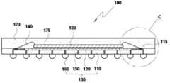
Translated fromKorean도 1a는 본 발명의 제1 실시예에 의한 패키지의 평면도이다.1A is a plan view of a package according to a first embodiment of the present invention.
도 1b는 도 1a의 A부분을 확대한 부분확대 평면도이다.FIG. 1B is a partially enlarged plan view illustrating an enlarged portion A of FIG. 1A.
도 1c는 도 1a의 배면도이다.FIG. 1C is a rear view of FIG. 1A.
도 1d는 도 1a의 BB′에 대한 단면도이다.FIG. 1D is a cross-sectional view taken along line BB ′ of FIG. 1A.
도 1e는 도 1d의 C부분을 확대한 부분확대 단면도이다.FIG. 1E is an enlarged cross-sectional view of part C of FIG. 1D.
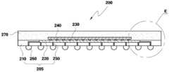
도 2a는 본 발명의 제2 실시예에 의한 패키지의 평면도이다.2A is a plan view of a package according to a second embodiment of the present invention.
도 2b는 도 2a의 배면도이다.FIG. 2B is a rear view of FIG. 2A.
도 2c는 도 2a의 DD′에 대한 단면도이다.FIG. 2C is a cross-sectional view taken along DD ′ of FIG. 2A.
도 2d는 도 2c의 E부분을 확대한 부분확대 단면도이다.FIG. 2D is an enlarged partial cross-sectional view of part E of FIG. 2C.
도 3은 본 발명의 반도체 집적회로에 대한 실시예로서 멀티플렉서를 포함하는 블록도이다.3 is a block diagram including a multiplexer as an embodiment of a semiconductor integrated circuit of the present invention.
도 4는 멀티플렉서의 논리회로도이다.4 is a logic circuit diagram of a multiplexer.
도 5는 도 4에 도시된 제3 낸드게이트(NAND3)를 나타낸 회로도이다.FIG. 5 is a circuit diagram illustrating the third NAND gate NAND3 illustrated in FIG. 4.
도 6은 본 발명의 반도체 집적회로에 대한 다른 실시예로서 전원 변환회로를 나타낸 회로도이다.6 is a circuit diagram illustrating a power conversion circuit as another embodiment of the semiconductor integrated circuit of the present invention.
도 7은 본 발명의 반도체 집적회로에 대한 실시예로서 개별 수동소자를 포함하는 회로 중 로우 패스필터를 나타낸 회로도이다.FIG. 7 is a circuit diagram illustrating a low pass filter in a circuit including individual passive devices as an embodiment of the semiconductor integrated circuit of the present invention.
본 발명은 패키지 회로기판 및 이를 이용한 패키지에 관한 것으로, 특히 미세전자소자 칩을 실장하기 위해 인쇄회로기판(Printed Circuit Board, 이하 PCB)을 대신하여 반도체 기판을 사용하는 패키지 회로기판 및 이를 이용한 패키지에 관한 것이다.The present invention relates to a package circuit board and a package using the same, and more particularly to a package circuit board using a semiconductor substrate instead of a printed circuit board (PCB) for mounting a microelectronic device chip and a package using the same. It is about.
칩의 소형화 및 고속화 추세에 따라 이에 사용되는 패키지 구조도 점차 경박 단소화의 추세로 발전하고 있다.As chip miniaturization and high-speed trend, the package structure used is gradually developing to the trend of light and short.
그리고, 칩의 고속화에 따라 종래의 저속 동작에서 문제가 되지 않았던 패키지의 전기적 특성이 칩의 동작 속도를 제한하는 주요 요인이 된다.In addition, due to the high speed of the chip, the electrical characteristics of the package, which has not been a problem in the conventional low speed operation, become a major factor limiting the operation speed of the chip.
한편, 패키지의 여러 요소 중에서도 칩의 내부와 외측을 연결하는 패키지 핀의 전기적인 성질이 고속 동작의 관건이 되기 때문에 핀의 물리적인 구조 및 배치 방식에 따라 여러 가지 다양한 패키지 구조가 제안되어 왔다.On the other hand, among the various elements of the package, since the electrical properties of the package pin connecting the inside and the outside of the chip is a key to high speed operation, various various package structures have been proposed according to the physical structure and arrangement of the pins.
저속에서 동작하는 칩 패키지는 리드 프레임(lead frame)과 상기 패키지의 일 측면에 일차원적으로 배치된 복수의 핀을 구비하고 있으며, 상기 리드 프레임(lead frame)을 이용하여 패키지의 변에 일정한 간격을 두고 복수개의 핀들을 일차원적으로 배치하는 경우가 대부분이었다.A chip package operating at a low speed includes a lead frame and a plurality of pins arranged one-dimensionally on one side of the package. The chip package uses a lead frame to provide a constant distance to the sides of the package. In most cases, a plurality of pins were arranged one-dimensionally.
그러나, 이 방법은 패키지의 크기가 소형화됨에 따라 수용할 수 있는 최대 핀 수에 제한이 생기게 되며, 칩 내부의 본딩 패드와 리드 프레임 간에 발생하는 인덕턴스 및 부가적인 커패시터, 저항 등의 간섭요인으로 고주파 동작에서의 전기적 특성이 떨어지기 때문에 고속 동작에는 적합하지 못하다.However, this method has a limit on the maximum number of pins that can be accommodated as the package size becomes smaller, and high frequency operation is caused by interference factors such as inductance and additional capacitors and resistors generated between the bonding pads and the lead frame inside the chip. It is not suitable for high speed operation because of its poor electrical characteristics.
리드 프레임을 이용한 패키지의 단점을 극복하고 패키지 크기를 소형화하기 위하여 칩 스케일 패키지(Chip scale package)가 개발되었다.Chip scale packages have been developed to overcome the disadvantages of packages using lead frames and to miniaturize package sizes.
칩 스케일 패키지는 패키지의 한쪽 면에 복수개의 핀(볼)들을 2차원 격자 형태로 배열할 수 있으며, 각 볼의 전기적인 기생 성분도 리드 프레임을 이용한 패키지에 비해서 줄일 수 있다는 장점이 있다. 따라서, 칩 스케일 패키지는 소형, 고속 동작용 패키지로 적합하다.The chip scale package can arrange a plurality of pins (balls) on one side of the package in a two-dimensional lattice form, and the electrical parasitics of each ball can be reduced compared to a package using a lead frame. Thus, chip scale packages are well suited for small, high speed operation packages.
칩 스케일 패키지의 대표적인 형태인 볼 그리드 어레이(ball grid array, 이하 BGA) 패키지는 기판과 기판 일면에 실장된 미세전자소자 칩과, 기판 타면에 형성되어 미세전자소자 칩과 전기적으로 연결된 I/O 핀(예를 들어, 솔더볼)을 포함한다. 여기서, 미세전자소자 칩은 기판에 의하여 지지되고, 기판을 통하여 미세전자소자 칩과 I/O 핀이 전기적으로 연결된다. 미국특허 제6,041,495호에서는 종래의 BGA 패키지를 상세히 개시하고 있다.A ball grid array (BGA) package, which is a representative type of chip scale package, is a microelectronic device chip mounted on a substrate and one side of the substrate, and an I / O pin formed on the other side of the substrate and electrically connected to the microelectronic device chip. (Eg, solder balls). Here, the microelectronic device chip is supported by the substrate, and the microelectronic device chip and the I / O pin are electrically connected through the substrate. US Patent No. 6,041,495 discloses a conventional BGA package in detail.
종래의 칩 스케일 패키지의 경우, 실장되는 미세전자소자 칩의 크기 정도로 패키지의 크기도 작아짐에 따라, 패키지의 크기를 결정하는 변수는 I/O 핀, 즉 솔더볼(Solder ball)의 개수가 되었다. 미세전자소자 칩에 기본적으로 요구되는 I/O 핀, 즉 솔더볼의 개수가 있으므로, 패키지의 소형화에 한계가 발생한다.In the case of the conventional chip scale package, as the size of the package is smaller as the size of the microelectronic chip to be mounted, the variable for determining the size of the package is the number of I / O pins, that is, solder balls. Since the number of I / O pins, that is, solder balls, which are basically required for the microelectronic device chip, there is a limit in miniaturization of the package.
SOC(System on chip)는 여러 기능의 반도체 설계자산(Intellectual property, 이하 IP)을 하나의 미세전자소자 칩에 집적하는 것을 기본으로 한다. 그러나, 기능의 고집접화로 인하여 IP가 증가하게 되고, IP의 증가에 따라 시그널(signal) 등이 전송되는 핀(볼)의 수가 증가하게 된다. 이는 결국 패키지의 크기가 커지는 결과를 초래한다.System on chip (SOC) is based on the integration of multiple functional semiconductor design assets (IP) into a single microelectronic chip. However, due to the high concentration of functions, IP increases, and as the IP increases, the number of pins (balls) through which signals and the like are transmitted increases. This results in a larger package size.
본 발명이 이루고자 하는 기술적 과제는, 반도체 기판을 회로기판으로 사용하여 회로기판 상에 능동소자(Active element) 또는 수동소자(Passive element)를 패턴형성하여 신호 입출력단자의 개수를 감소시켜 소형화할 수 있고, 패키지 제품 특성을 향상시킬 수 있는 패키지 회로기판을 제공하고자 하는 것이다.The technical problem to be achieved by the present invention can be miniaturized by reducing the number of signal input and output terminals by patterning an active element or a passive element on a circuit board using a semiconductor substrate as a circuit board. The present invention aims to provide a package circuit board that can improve package product characteristics.
본 발명이 이루고자 하는 다른 기술적 과제는, 반도체 기판을 회로기판으로 사용하여 회로기판 상에 능동소자(Active element) 또는 수동소자(Passive element)를 패턴형성하여 신호 입출력단자의 개수를 감소시켜 소형화할 수 있고, 패키지 제품 특성을 향상시킬 수 있는 패키지 회로기판을 이용한 패키지를 제공하고자 하는 것이다.Another technical object of the present invention is to reduce the number of signal input and output terminals by patterning an active element or a passive element on a circuit board using a semiconductor substrate as a circuit board. In addition, to provide a package using a package circuit board that can improve the package product characteristics.
상기 기술적 과제를 달성하기 위한 본 발명의 일 실시예에 따른 패키지 회로기판은, 반도체 기판과, 상기 반도체 기판의 일면에 형성되고, 미세전자소자 칩에 대한 입출력 신호를 처리하는 반도체 집적회로와, 상기 반도체 기판의 타면에 형성되고, 상기 반도체 집적회로와 전기적 연결수단에 의해 연결된 신호 입출력단자를 포함한다.According to an aspect of the present invention, there is provided a package circuit board including a semiconductor substrate, a semiconductor integrated circuit formed on one surface of the semiconductor substrate, and processing an input / output signal to a microelectronic device chip; It is formed on the other surface of the semiconductor substrate, and includes a signal input and output terminal connected by the semiconductor integrated circuit and the electrical connection means.
또한, 상기 다른 기술적 과제를 달성하기 위한 본 발명의 일 실시예에 따른 패키지는, 미세전자소자 칩과, 반도체 기판과 상기 반도체 기판의 일면에 형성되고 상기 미세전자소자 칩과 제1 전기적 연결수단에 의해 연결되어 상기 미세전자소자 칩에 대한 입출력 신호를 처리하는 반도체 집적회로와 상기 반도체 기판의 타면에 형성되고 상기 반도체 집적회로와 제2 전기적 연결수단에 의해 연결된 신호 입출력단자를 구비하는 패키지 회로기판를 포함한다.In addition, the package according to an embodiment of the present invention for achieving the other technical problem, is formed on the microelectronic device chip, the semiconductor substrate and one surface of the semiconductor substrate and the microelectronic device chip and the first electrical connection means And a package circuit board connected to each other to process an input / output signal to the microelectronic device chip, and a signal input / output terminal formed on the other surface of the semiconductor substrate and connected by the semiconductor integrated circuit and a second electrical connection means. do.
기타 실시예들의 구체적인 사항들은 상세한 설명 및 도면들에 포함되어 있다.Specific details of other embodiments are included in the detailed description and the drawings.
본 발명의 이점 및 특징, 그리고 그것들을 달성하는 방법은 첨부되는 도면과 함께 상세하게 후술되어 있는 실시예들을 참조하면 명확해질 것이다. 그러나 본 발명은 이하에서 개시되는 실시예들에 한정되는 것이 아니라 서로 다른 다양한 형태로 구현될 것이며, 단지 본 실시예들은 본 발명의 개시가 완전하도록 하며, 본 발명이 속하는 기술분야에서 통상의 지식을 가진 자에게 발명의 범주를 완전하게 알려주기 위해 제공되는 것이며, 본 발명은 청구항의 범주에 의해 정의될 뿐이다. 명세서 전체에 걸쳐 동일 참조 부호는 동일 구성 요소를 지칭한다.Advantages and features of the present invention and methods for achieving them will be apparent with reference to the embodiments described below in detail with the accompanying drawings. However, the present invention is not limited to the embodiments disclosed below, but may be implemented in various forms. It is provided to fully convey the scope of the invention to those skilled in the art, and the present invention is defined only by the scope of the claims. Like reference numerals refer to like elements throughout.
이하 본 발명의 실시예에 따른 미세전자소자 칩은 DRAM, SRAM, 플래쉬 메모리 등의 고집적 반도체 메모리 칩, MEMS(Micro Electro Mechanical Systems) 칩, 광전자 (optoelectronic) 소자 칩, 또는 CPU, DSP 등의 프로세서 등을 포함한다. 따라서, 미세전자소자 칩은 동일 종류의 전자소자 칩들로만 구성될 수도 있고, 하 나의 완전한 기능을 제공하기 위해서 필요한 서로 다른 종류의 전자소자 칩들로 구성될 수도 있다.The microelectronic device chip according to an embodiment of the present invention is a highly integrated semiconductor memory chip such as DRAM, SRAM, flash memory, MEMS (Micro Electro Mechanical Systems) chip, optoelectronic device chip, or a processor such as a CPU, DSP, etc. It includes. Therefore, the microelectronic device chip may be composed of only the same kind of electronic device chips, or may be composed of different kinds of electronic device chips required to provide one complete function.
여기서, 하나의 완전한 기능을 제공하기 위해서 필요한 서로 다른 종류의 전자소자 칩들로 구성된 단일 칩 데이터 처리 장치는, 프로세서, 메모리, 및 주변 장치로 구성된다. 프로세서로는 CISC(복합 명령 세트 컴퓨팅) CPU, 또는 RISC(축소 명령 세트 컴퓨팅) CPU 등이 사용된다. DSP(Digital Signal Processor) 또는 CPU 와 DSP의 조합이 프로세서로 사용될 수도 있다. 메모리는 휘발성 메모리(SRAM. DRAM) 및/또는 비휘발성 메모리(마스크 ROM, EEPROM, Flash)로 구성될 수 있다. 주변 장치는 디텍터(detector), 카운터/타이머, I/O, 콘트롤러 등의 일반 장치 또는 LCD 콘트롤러, 그래픽스 콘트롤러, 네트워크 콘트롤러 등의 특수 목적 장치 등으로 다양하다. 데이터 처리 장치가 데이터 저장, 데이터의 인출 및 처리 등을 원활하게 수행하도록 이들 프로세서, 메모리 및 주변 장치는 주소 버스, 데이터 버스 및 콘트롤 버스 등에 의해 유기적으로 연결되어 있다.Here, a single chip data processing device composed of different kinds of electronic device chips required to provide one complete function is composed of a processor, a memory, and a peripheral device. As a processor, a CISC (Complex Instruction Set Computing) CPU, a RISC (Reduced Instruction Set Computing) CPU, or the like is used. A digital signal processor (DSP) or a combination of CPU and DSP may be used as the processor. The memory may be comprised of volatile memory (SRAM. DRAM) and / or nonvolatile memory (mask ROM, EEPROM, Flash). Peripheral devices may be general devices such as detectors, counters / timers, I / Os, controllers, or special purpose devices such as LCD controllers, graphics controllers, and network controllers. The processors, memory, and peripherals are organically connected by an address bus, a data bus, a control bus, and the like so that the data processing device can perform data storage, data retrieval, processing, and the like smoothly.
또한, 본 발명에 따른 미세전자소자 칩이 실장되는 패키지 회로기판을 구성하는 반도체 기판은 실리콘 웨이퍼, SOI(Silicon On Insulator) 웨이퍼, 갈륨 비소 웨이퍼, 실리콘 게르마늄 웨이퍼, 세라믹 웨이퍼, 석영 웨이퍼 등이 있으나, 이는 예시적인 것에 불과하다.In addition, the semiconductor substrate constituting the package circuit board on which the microelectronic device chip according to the present invention is mounted includes a silicon wafer, a silicon on insulator (SOI) wafer, a gallium arsenide wafer, a silicon germanium wafer, a ceramic wafer, a quartz wafer, and the like. This is merely illustrative.
이러한 반도체 기판은 미세가공이 용이하여 그 위에 실장되는 미세전자소자 칩의 동작의 효율성 또는 유용성 향상에 필요한 다양한 반도체 집적회로를 구성하는 것이 가능하다. 여기서, 반도체 집적회로는 미세전자소자 칩에 따라 다양한 형 태로 구현될 수 있는데, 예를 들어 미세전자소자 칩이 선택적으로 활성화되는 2 이상의 구성요소를 포함하는 경우 멀티플렉서 회로를 반도체 집적회로로 사용할 수 있고, 미세전자소자 칩이 2 이상의 서로 다른 전원전압을 필요로 하는 경우 전압변환 회로를 반도체 집적회로로 사용할 수 있다.Such a semiconductor substrate is easy to microfabricate, it is possible to configure a variety of semiconductor integrated circuits required for improving the efficiency or usability of the operation of the microelectronic device chip mounted thereon. Here, the semiconductor integrated circuit may be implemented in various forms according to the microelectronic device chip. For example, when the microelectronic device chip includes two or more components selectively activated, the multiplexer circuit may be used as the semiconductor integrated circuit. When the microelectronic device chip requires two or more different power supply voltages, the voltage conversion circuit may be used as a semiconductor integrated circuit.
이하, 도 1a 내지 도 1e를 참조하여 본 발명의 제1 실시예를 상세히 설명한다.Hereinafter, a first embodiment of the present invention will be described in detail with reference to FIGS. 1A to 1E.
도 1a는 본 발명의 제1 실시예에 의한 패키지의 평면도이다. 도 1b는 도 1a의 A부분을 확대한 부분확대 평면도이다. 도 1c는 도 1a의 배면도이다. 도 1d는 도 1a의 BB′에 대한 단면도이다. 그리고, 도 1e는 도 1d의 C부분을 확대한 부분확대 단면도이다.1A is a plan view of a package according to a first embodiment of the present invention. FIG. 1B is a partially enlarged plan view illustrating an enlarged portion A of FIG. 1A. FIG. 1C is a rear view of FIG. 1A. FIG. 1D is a cross-sectional view taken along line BB ′ of FIG. 1A. 1E is a partially enlarged cross-sectional view illustrating an enlarged portion C of FIG. 1D.
도 1a 내지 도 1e에 도시된 바와 같이, 본 발명의 제1 실시예에 의한 패키지(100)는 패키지 회로기판(105)과 그 위에 실장된 미세전자소자 칩(130)으로 구성된다. 이 패키지 회로기판(105)은 반도체 기판(110)과, 반도체 기판(110)의 일면에 패턴되어 형성된 반도체 집적회로(120)와, 비아홀(150)과 연결된 신호 입출력단자(160)로 구성된다.1A to 1E, the
여기서, 반도체 기판(110)은 대표적인 예로 실리콘(Si) 기판을 사용할 수 있다.Here, the
그리고, 미세전자소자 칩(130)은 반도체 기판(110)의 일면에 실장되어 외부로부터의 신호를 처리하는 역할을 한다.The
본 실시예에 의한 패키지(100)에서, 미세전자소자 칩(130)은 반도체 기판(110)과 와이어 본딩(Wire Bonding)(140)에 의해 전기적으로 연결된다. 도 1b에 도시된 바와 같이, 반도체 기판(110) 상에 형성된 기판패드(115)와 미세전자소자 칩(130) 상에 형성된 칩패드(135)가 와이어 본딩(140)에 의해 전기적으로 연결된다.In the
그리고, 도 1c에 도시된 바와 같이, 반도체 기판(110)의 배면에는 다수의 신호 입출력단자(160)가 격자(grid) 형태로 배치된다. 여기서, 신호 입출력단자(160)로는 솔더볼(Solder ball)을 사용할 수 있다.As illustrated in FIG. 1C, a plurality of signal input /
이하, 도 1b, 도 1d 및 도 1e를 참조하여 미세전자소자 칩(130)과 신호 입출력단자(160) 간의 입출력 신호가 전달되는 경로를 살펴본다.Hereinafter, a path through which an input / output signal is transmitted between the
미세전자소자 칩(130) 상에 형성된 칩패드(135)와 반도체 기판(110) 상에 형성된 기판패드(115)가 와이어 본딩(140)에 의해 전기적으로 연결되고, 이러한 기판패드(115)는 제2 배선패턴(120b)을 통하여 반도체 집적회로(120)와 전기적으로 연결된다. 그리고, 반도체 집적회로(120)와 신호 입출력단자(160)는 제1 배선패턴(120a)과 비아 홀(via hole)(150) 내의 도전성 물질에 의해 전기적으로 연결된다.The
반도체 기판(110)의 소정의 부분에 에칭기술 또는 레이저를 이용하여 비아 홀(150)을 형성한다. 비아 홀(150)은 반도체 기판(110)의 상면에 형성된 반도체 집적회로(120)와 제1 배선패턴(120a)에 의해 전기적으로 연결되고, 반도체 기판(110)의 하면에 형성된 신호 입출력단자(160)와 전기적으로 연결된다. 비아 홀(150)의 내부를 충진하는 도전성 물질로는 Cu, Al, Ag, Au, Ni 등을 사용하는 것이 바람직 하다. 이러한 도전성 물질은 스퍼터링(sputtering), 화학기상증착(Chemical vapor deposition) 또는 전기도금(electroplating) 등의 방법으로 형성할 수 있다.The via
미세전자소자 칩(130)에 대한 입출력 신호는 반도체 집적회로(120)를 통과하여 소정의 전기적 신호처리를 수행한 후, 신호 입출력단자(160)를 통하여 외부로 전달된다.The input / output signal to the
이러한 패키지(100)가 메모리 디바이스를 구성할 때, 신호 입출력단자(160)는 어드레스 및 명령 신호를 전달하고 데이터를 입출력한다.When the
도 1d 및 도 1e에 도시된 바와 같이, 미세전자소자 칩(130)과 와이어 본딩(140)을 절연성 봉지수지(170)로 봉지하는 것이 바람직하다. 여기서, 절연성 봉지수지(170)는 전기적으로 접합된 부분의 신뢰성의 향상과 접합 부분의 강도의 보강을 도모한다. 절연성 봉지수지(170)로는 절연성의 에폭시 수지, 절연성의 실리콘 수지 등이 사용될 수 있다.As illustrated in FIGS. 1D and 1E, the
이하, 도 2a 내지 도 2d를 참조하여 본 발명의 제2 실시예를 상세히 설명한다.Hereinafter, a second embodiment of the present invention will be described in detail with reference to FIGS. 2A to 2D.
도 2a는 본 발명의 제2 실시예에 의한 패키지의 평면도이다. 도 2b는 도 2a의 배면도이다. 도 2c는 도 2a의 DD′에 대한 단면도이다. 그리고, 도 2d는 도 2c의 E부분을 확대한 부분확대 단면도이다.2A is a plan view of a package according to a second embodiment of the present invention. FIG. 2B is a rear view of FIG. 2A. FIG. 2C is a cross-sectional view taken along DD ′ of FIG. 2A. 2D is a partially enlarged cross-sectional view showing an enlarged portion E of FIG. 2C.
도 2a 내지 도 2d에 도시된 바와 같이, 본 발명의 제2 실시예에 의한 패키지(200)는 패키지 회로기판(205)과 그 위에 실장된 미세전자소자 칩(230)으로 구성된다. 이 패키지 회로기판(205)은 반도체 기판(210)과, 반도체 기판(210)의 일 면에 패턴되어 형성된 반도체 집적회로(220)와, 비아홀(250)과 연결된 신호 입출력단자(260)로 구성된다.As shown in FIGS. 2A to 2D, the
여기서, 반도체 기판(210)은 대표적인 예로 실리콘(Si) 기판을 사용할 수 있다.The
그리고, 미세전자소자 칩(230)은 반도체 기판(210)의 일면에 실장되어 외부로부터의 신호를 처리하는 역할을 한다.The
본 실시예에 의한 패키지(200)에서, 미세전자소자 칩(230)은 반도체 기판(210)과 플립칩 본딩(Flip chip Bonding)(240)에 의해 전기적으로 연결된다. 도 2d에 도시된 바와 같이, 반도체 기판(210) 상에 형성된 기판패드(215)와 미세전자소자 칩(230)은 플립칩 본딩(240)에 의해 전기적으로 연결된다.In the
그리고, 도 2b에 도시된 바와 같이, 반도체 기판(210)의 배면에는 다수의 신호 입출력단자(260)가 격자(grid)를 따라 배치된다. 여기서, 신호 입출력단자(260)로는 솔더볼(Solder ball)을 사용할 수 있다.As illustrated in FIG. 2B, a plurality of signal input /
이하, 도 2d를 참조하여 미세전자소자 칩(230)과 신호 입출력단자(260) 간의 입출력 신호가 전달되는 경로를 살펴본다.Hereinafter, a path through which an input / output signal is transmitted between the
미세전자소자 칩(230)과 반도체 기판(210) 상에 형성된 기판패드(215)가 플립칩 본딩(240)에 의해 전기적으로 연결되고, 이러한 기판패드(215)는 반도체 집적회로(220)와 전기적으로 연결된다. 그리고, 반도체 집적회로(220)와 신호 입출력단자(260)는 배선패턴(220a)과 비아 홀(via hole)(250) 내의 도전성 물질에 의해 전기적으로 연결된다. 본 실시예에서의 비아 홀(250)은 제1 실시예에서의 비아 홀(250)과 동일한 방법으로 제조하고, 동일한 물질로 충진한다.The
미세전자소자 칩(230)에 대한 입출력 신호는 반도체 집적회로(220)를 통과하여 소정의 전기적 신호처리를 수행한 후, 신호 입출력단자(260)를 통하여 외부로 전달된다.The input / output signal to the
이러한 패키지가(200)가 메모리 디바이스를 구성할 때, 신호 입출력단자(260)는 어드레스 및 명령 신호를 전달하고 데이터를 입출력한다.When the
도 2c 및 도 2d에 도시된 바와 같이, 미세전자소자 칩(230)과 플립칩 본딩(240)을 절연성 봉지수지(270)로 봉지하는 것이 바람직하다.As illustrated in FIGS. 2C and 2D, the
이하, 제1 실시예와 제2 실시예에서 설명한 반도체 집적회로를 자세히 설명한다.Hereinafter, the semiconductor integrated circuits described in the first and second embodiments will be described in detail.
도 3은 본 발명의 반도체 집적회로에 대한 실시예로서 멀티플렉서(Multiplexor)를 포함하는 블록도이다.3 is a block diagram including a multiplexer as an embodiment of a semiconductor integrated circuit of the present invention.
도면부호 300은 미세전자소자 칩(130, 230)을 구성하는 모듈들을 나타내고, 도면부호 350은 반도체 기판(110, 210)의 일면에 형성된 반도체 집적회로(120, 220)를 나타내고, 도면부호 360은 솔더볼(또는 핀)과 같은 외부 입출력단자(160, 260)를 나타내는 것이다.
기본 입출력 시스템인 BIOS의 셋업(Setup) 정보를 저장하고 있는 기억장치로 사용되는 ROM 또는 캐쉬메모리로 사용되는 SRAM의 경우, 어드레스 버스(Address bus)(310)와 데이터 버스(Data bus)(315)는 동시에 동작하지 않는다. 따라서, ROM 또는 SRAM의 어드레스 버스(310)와 ROM 또는 SRAM의 데이터 버스(315)에 제1 멀티 플렉서(352)를 연결하여, I/O 핀을 공유할 수 있다. 예를 들어, ROM 또는 SRAM의 어드레스 버스(310)를 위해 26 핀(Pin)이 할당되고 ROM 또는 SRAM의 데이터 버스(315)를 위해 15 핀이 할당되는 경우, 제1 멀티플렉서(352)를 연결하면 총 필요한 신호 입출력단자(360)의 수가 41 핀에서 26 핀으로 줄어드는 효과가 있다.In the case of ROM used as a storage device for storing setup information of the basic input / output system BIOS or SRAM used as cache memory, an
그리고, 메인 메모리로 사용되는 SDRAM에서 제1 뱅크(Bank)(320, 325)와 제2 뱅크(330, 335)가 있는 경우, SDRAM의 제1 뱅크(320, 325)와 SDRAM의 제2 뱅크(330, 335)는 동시에 동작하지 않는다. 따라서, 각 뱅크의 어드레스 버스(320, 330) 또는 데이터 버스(325, 335)는 공유할 수 있다. 즉, SDRAM 제1 뱅크의 어드레스 버스(320)와 SDRAM 제2 뱅크의 어드레스 버스(330)를 제2 멀티플렉서(354)에 연결하고, SDRAM 제1 뱅크의 데이터 버스(325)와 SDRAM 제2 뱅크의 데이터 버스(335)를 제3 멀티플렉서(356)에 연결하여, I/O 핀을 공유할 수 있다. 예를 들어, SDRAM 제1 뱅크의 어드레스 버스(320)와 SDRAM 제2 뱅크의 어드레스 버스(330)를 위해 각각 15 핀이 할당되고, SDRAM 제1 뱅크의 데이터 버스(325)와 SDRAM 제2 뱅크의 데이터 버스(335)를 위해 각각 32 핀이 할당되는 경우, 제2 멀티플렉서(354)와 제3 멀티플렉서(356)를 이용하면 총 필요한 신호 입출력단자(360)의 수가 94 핀에서 47 핀으로 줄어드는 효과가 있다.If there are
이상, 멀티플렉서의 실시 태양으로서 ROM 또는 SRAM의 어드레스 버스(310)와 데이터 버스(315) 사이의 멀티플렉서(352)와, SDRAM의 제1 뱅크(320, 325)와 제2 뱅크(330, 335) 사이의 멀티플렉서(354, 356)를 언급하지만, 이는 예시적인 것이 불과하다.As described above, as an embodiment of the multiplexer, the
도 4는 멀티플렉서의 논리회로도이다.4 is a logic circuit diagram of a multiplexer.
도 4에 도시된 바와 같이, 멀티플렉서 회로는, 제1 클럭 신호(clkA)와 제어 신호(sel)의 반전 신호를 입력받는 제1 NAND 게이트(NAND1)와, 제어 신호(sel)와 제2 클럭 신호(clkB)를 입력받는 제2 NAND 게이트(NAND2)와, 제1 NAND 게이트(NAND1)의 출력 신호(in1)와 제2 NAND 게이트(NAND2)의 출력 신호(in2)를 입력받는 제3 NAND 게이트(NAND3)와, 제3 NAND 게이트(NAND3)의 출력 신호(out)를 수신하여 반전된 신호(clk_out)를 출력하는 인버터(IV2)로 구성되어 있다.As shown in FIG. 4, the multiplexer circuit includes a first NAND gate NAND1, a control signal sel, and a second clock signal that receive an inverted signal of the first clock signal clkA and the control signal sel. The second NAND gate NAND2 receiving the clkB, the third NAND gate receiving the output signal in1 of the first NAND gate NAND1 and the output signal in2 of the second NAND gate NAND2 ( NAND3 and an inverter IV2 that receives the output signal out of the third NAND gate NAND3 and outputs the inverted signal clk_out.
멀티플렉서 회로는 제어 신호(sel)에 따라 제1 클럭 신호(clkA)와 제2 클럭 신호(clkB) 중 하나를 출력 신호(clk_out)로 출력한다.The multiplexer circuit outputs one of the first clock signal clkA and the second clock signal clkB as an output signal clk_out according to the control signal sel.
도 5는 도 4에 도시된 제3 낸드게이트(NAND3)를 나타낸 회로도이다.FIG. 5 is a circuit diagram illustrating the third NAND gate NAND3 illustrated in FIG. 4.
도 5에 도시된 바와 같이, 제3 낸드게이트(NAND3)는 전원 전압(Vcc)과 출력 단자(out) 사이에 병렬로 접속되며 게이트에 제1 NAND 게이트(NAND1)의 출력 신호(in1)와 제2 NAND 게이트(NAND2)의 출력 신호(in2)를 각각 입력받는 PMOS 트랜지스터(P1, P2)와, 출력 단자(out)와 접지 전압(Vss) 사이에 직렬로 접속되며 게이트에 제1 NAND 게이트(NAND1)의 출력 신호(in1)와 제2 NAND 게이트(NAND2)의 출력 신호(in2)를 각각 입력받는 NMOS 트랜지스터(N1, N2)로 구성되어 있다.As illustrated in FIG. 5, the third NAND gate NAND3 is connected in parallel between the power supply voltage Vcc and the output terminal out, and the output signal in1 of the first NAND gate NAND1 and the first NAND gate NAND1 are connected to the gate. 2 is connected in series between the PMOS transistors P1 and P2 which receive the output signal in2 of the NAND gate NAND2, and the output terminal out and the ground voltage Vss, respectively, and the first NAND gate NAND1 is connected to the gate. NMOS transistors N1 and N2 that receive the output signal in1 of the signal output signal in1 and the output signal in2 of the second NAND gate NAND2, respectively.
제3 낸드게이트(NAND3)는 출력 신호(in1)와 출력 신호(in2)가 모두 로우(Low)를 가지거나 어느 하나가 로우를 가지면 출력 단자(out)로 하이(High)를 출력한다. 그리고, 출력 신호(in1)와 출력 신호(in2)가 모두 하이를 가질 때 NMOS 트랜지스터(N1, N2)가 모두 동작하여 출력 단자(out)로 로우를 출력한다.The third NAND gate NAND3 outputs high to the output terminal out when both the output signal in1 and the output signal in2 have a low or one has a low. When both the output signal in1 and the output signal in2 have a high value, both the NMOS transistors N1 and N2 operate to output a low to the output terminal out.
도 6은 본 발명의 반도체 집적회로에 대한 다른 실시예로서 전원 변환회로를 나타낸 회로도이다.6 is a circuit diagram illustrating a power conversion circuit as another embodiment of the semiconductor integrated circuit of the present invention.
도 6에 도시된 바와 같이, 전원 변환회로는 저항(R1, R2, R3)와 오피엠프(Op-Amp1, Op-Amp2)와 로드 커패시터(Load Capacitor)(C1, C2)로 구성된다.As shown in FIG. 6, the power conversion circuit includes resistors R1, R2 and R3, op amps Op-Amp1 and Op-Amp2, and load capacitors C1 and C2.
시스템 보드(System board)로부터 신호 입출력단자(160, 260)를 통하여 패키지(100, 200)로 전압(V1)이 공급된다. 저항(R1, R2, R3)의 크기에 비례하여 로드 커패시터(C1, C2)에 출력되는 전압(V2, V3)이 달라진다.The voltage V1 is supplied from the system board to the
즉, 전압(V2)와 전압(V3)는 수학식1과 수학식2를 만족한다.That is, the voltage V2 and the voltage V3 satisfy the equations (1) and (2).
[수학식 1][Equation 1]

[수학식 2][Equation 2]

예를 들어, 272 핀을 가진 FBGA(Fine pitch BGA)의 경우, 3.3 V의 전원전압(V1)에 26 핀, 2.5 V의 전원전압(V2)에 26 핀, 1.2 V의 전원전압(V3)에 3 핀이 필요하다. 하지만, 본 발명의 일 실시예인 전원 변환회로를 가진 반도체 기판을 적용하면 2.5 V의 전원전압(V2)과 1.2 V의 전원전압(V3)을 위한 핀, 즉 신호 입출력단자(160, 260)는 더 이상 필요가 없게 된다. 그리고, 3.3V의 전원전압(V1)의 경우 패키지에 원활하고 안정된 전원전압을 공급하기 위해 많은 수의 핀, 즉 26핀을 사용하였다. 하지만, 본 발명의 일 실시예에 의한 반도체 기판 상에 전원 변환회로와 더불어 커패시터와 같은 수동소자를 형성한 후 이들을 통하여 시스템 보드로부터 미세전자소자 칩에 전원전압을 공급하는 경우 반도게 기판 상에 형성된 커패시터가 전원전압을 안정화하는 역할을 하므로 종래 기술에 의한 패키지보다 적은 수의 핀을 사용하여도 원활하고 안정된 전원전압을 공급할 수 있다. 따라서, 3.3 V의 전원전압(V1)을 위한 핀도 10 핀 이하로 축소될 수 있는 효과가 있다.For example, FBGA (Fine pitch BGA) with 272 pins has 26 pins at 3.3 V power supply voltage (V1), 26 pins at 2.5 V power supply voltage (V2), and 1.2 V power supply voltage (V3). 3 pins are required. However, when the semiconductor substrate having the power conversion circuit according to the embodiment of the present invention is applied, the pins for the power supply voltage V2 of 2.5 V and the power supply voltage V3 of 1.2 V, that is, the signal input /
따라서, 전원 변환회로를 내장한 패키지 회로기판을 사용한 패키지의 경우 총 전원전압(V1, V2, V3)에 필요한 신호 입출력단자(160, 260)가 55 핀에서 10 핀 이하로 줄어들게 되어 약 80 %의 핀 감소 효과를 얻을 수 있다. 이러한 핀 개수의 감소는 패키지의 소형화에 직접적인 요인이 된다. 또한, 전원 변환회로를 내장한 반도체 기판을 사용한 패키지를 사용할 경우, 시스템 보드를 설계할 때 하나의 전원전압만 패키지에 전달하게 되어 좀더 쉽게 시스템 보드를 설계할 수 있다.Therefore, in the case of a package using a package circuit board incorporating a power conversion circuit, the signal input /
SOC에서 다양한 IP에 제공되는 다양한 전원에 대하여 시스템 보드에서 패키지(100, 200)에 하나의 전원을 공급한 후, 패키지(100, 200) 내의 반도체 기판(110, 210)에 전원 변환회로를 통하여 다양한 크기의 전원으로 변환되어 각 IP에 제공될 수 있다. 이로써, 각 IP의 전원에 대한 신호 입출력단자(160, 260)가 하나의 신호 입출력단자(160, 260)로 줄어드는 효과가 있다.After supplying one power to the
본 발명의 일 실시예에서는 전원전압의 감압회로만을 예로 들어 설명하였으나, 이에 한정되지 않으며 전원전압의 승압회로를 적용할 수도 있다.In the exemplary embodiment of the present invention, only the pressure reducing circuit of the power supply voltage has been described as an example, but the present invention is not limited thereto.
본 발명의 반도체 집적회로에 대한 또 다른 실시예로서 개별 수동소자를 포함하는 회로를 예로 들 수 있다. 이러한 개별 수동소자를 포함하는 회로는 커패시터, 인덕터, 저항, 또는 이들의 조합으로 구성된 패스필터(pass filter)로 구성될 수 있다.Another embodiment of the semiconductor integrated circuit of the present invention is a circuit including an individual passive element. The circuit including such individual passive elements may be composed of a pass filter composed of a capacitor, an inductor, a resistor, or a combination thereof.
개별 수동소자를 포함하는 회로 중 커패시터의 경우, 미세전자소자 칩(130, 230)의 고속 (100 MHz이상) 동작 시에 공급전원(Power supply)에 변동(Fluctuation)이 발생하는데, 미세전자소자 칩(130, 230)에 커패시터를 연결하면 안정된 고속 동작을 구현할 수 있다. 이러한 커패시터는 공급전원의 유도성 경로(Inductive path)를 최소화하고, 또한 부분전지(Local battery)의 역할을 한다.In the case of a capacitor in a circuit including individual passive devices, fluctuations occur in a power supply when the
도 7은 본 발명의 반도체 집적회로에 대한 실시예로서 개별 수동소자를 포함하는 회로 중 로우 패스필터(Low pass filter)를 나타낸 회로도이다.FIG. 7 is a circuit diagram illustrating a low pass filter among circuits including individual passive devices as an embodiment of the semiconductor integrated circuit of the present invention.
도 7에 도시된 바와 같이, 로우 패스필터(400)는 저항(410), 인덕터(420), 커패시터(430) 등의 개별적인 수동 소자가 사용될 수 있다.As illustrated in FIG. 7, the
이와 같이 수동소자 등을 반도체 기판 상에 패턴을 형성함으로써 시스템 보드 상에 수동 소자를 형성하는 종래의 시스템에 비해 시스템의 소형화를 추구할 수 있다. 나아가 개별적인 수동소자를 연결하여 로우 패스필터, 하이 패스필터 등의 회로를 구성함으로써 미세전자소자 칩의 동작 특성을 향상시킬 수 있다.Thus, by forming a passive element or the like on a semiconductor substrate, the system can be miniaturized as compared with the conventional system in which the passive element is formed on the system board. Furthermore, by connecting individual passive devices, circuits such as a low pass filter and a high pass filter can be configured to improve operating characteristics of the microelectronic chip.
이상 첨부된 도면을 참조하여 본 발명의 실시예를 설명하였지만, 본 발명이 속하는 기술분야에서 통상의 지식을 가진 자는 본 발명의 기술적 사상이나 필수적인 특징을 변경하지 않고서 다른 구체적인 형태로 실시될 수 있다는 것을 이해할 수 있을 것이다. 그러므로 이상에서 기술한 실시예들은 모든 면에서 예시적인 것이며 한정적이 아닌 것으로 이해해야만 한다.Although the embodiments of the present invention have been described above with reference to the accompanying drawings, those skilled in the art to which the present invention pertains may be embodied in other specific forms without changing the technical spirit or essential features of the present invention. I can understand. Therefore, it should be understood that the embodiments described above are exemplary in all respects and not restrictive.
상술한 바와 같이 본 발명에 따른 패키지 회로기판 및 이를 이용한 패키지에 의하면, 소형화되고 제품의 특성이 향상된 패키지 회로기판 및 이를 이용한 패키지를 제조할 수 있다.As described above, according to the package circuit board and the package using the same according to the present invention, the package circuit board and the package using the same can be manufactured.
Claims (19)
Translated fromKoreanPriority Applications (7)
| Application Number | Priority Date | Filing Date | Title |
|---|---|---|---|
| KR1020040000908AKR100541655B1 (en) | 2004-01-07 | 2004-01-07 | Package Circuit Board and Package Using the Same |
| US11/028,553US7663221B2 (en) | 2004-01-07 | 2005-01-05 | Package circuit board with a reduced number of pins and package including a package circuit board with a reduced number of pins and methods of manufacturing the same |
| JP2005000958AJP4926405B2 (en) | 2004-01-07 | 2005-01-05 | Package circuit board and package using the same |
| CNB2005100677821ACN100472762C (en) | 2004-01-07 | 2005-01-07 | Packaged circuit board and method of forming same |
| DE200510001856DE102005001856A1 (en) | 2004-01-07 | 2005-01-07 | Printed circuit board, manufacturing and voltage providing method |
| US12/654,991US20100117451A1 (en) | 2004-01-07 | 2010-01-12 | Package circuit board with a reduced number of pins and package including a package circuit board with a reduced number of pins and methods of manufacturing the same |
| JP2011258976AJP5302379B2 (en) | 2004-01-07 | 2011-11-28 | Package circuit board and package using the same |
Applications Claiming Priority (1)
| Application Number | Priority Date | Filing Date | Title |
|---|---|---|---|
| KR1020040000908AKR100541655B1 (en) | 2004-01-07 | 2004-01-07 | Package Circuit Board and Package Using the Same |
Publications (2)
| Publication Number | Publication Date |
|---|---|
| KR20050072564A KR20050072564A (en) | 2005-07-12 |
| KR100541655B1true KR100541655B1 (en) | 2006-01-11 |
Family
ID=34709328
Family Applications (1)
| Application Number | Title | Priority Date | Filing Date |
|---|---|---|---|
| KR1020040000908AExpired - Fee RelatedKR100541655B1 (en) | 2004-01-07 | 2004-01-07 | Package Circuit Board and Package Using the Same |
Country Status (5)
| Country | Link |
|---|---|
| US (2) | US7663221B2 (en) |
| JP (2) | JP4926405B2 (en) |
| KR (1) | KR100541655B1 (en) |
| CN (1) | CN100472762C (en) |
| DE (1) | DE102005001856A1 (en) |
Families Citing this family (24)
| Publication number | Priority date | Publication date | Assignee | Title |
|---|---|---|---|---|
| KR100541655B1 (en)* | 2004-01-07 | 2006-01-11 | 삼성전자주식회사 | Package Circuit Board and Package Using the Same |
| DE102004036469A1 (en)* | 2004-07-28 | 2006-02-16 | Fraunhofer-Gesellschaft zur Förderung der angewandten Forschung e.V. | Camera module, array based thereon and method for its production |
| JP5511119B2 (en)* | 2006-04-14 | 2014-06-04 | 株式会社リキッド・デザイン・システムズ | Interposer and semiconductor device |
| EP1878692B1 (en)* | 2006-07-14 | 2011-04-20 | STMicroelectronics Srl | Semiconductor package for MEMS devices |
| JP2008033724A (en)* | 2006-07-31 | 2008-02-14 | Mitsumi Electric Co Ltd | Single-chip semiconductor integrated circuit device manufacturing method, program debugging method, and microcontroller manufacturing method |
| JP5110247B2 (en)* | 2006-07-31 | 2012-12-26 | ミツミ電機株式会社 | Semiconductor integrated circuit device |
| JP5080762B2 (en)* | 2006-07-31 | 2012-11-21 | ミツミ電機株式会社 | Semiconductor integrated circuit device |
| JP2008053319A (en)* | 2006-08-22 | 2008-03-06 | Nec Electronics Corp | Semiconductor device |
| DE102006044016A1 (en)* | 2006-09-15 | 2008-04-03 | Fraunhofer-Gesellschaft zur Förderung der angewandten Forschung e.V. | Stackable functional layer for a modular microelectronic system |
| US8058960B2 (en)* | 2007-03-27 | 2011-11-15 | Alpha And Omega Semiconductor Incorporated | Chip scale power converter package having an inductor substrate |
| US7948346B2 (en)* | 2008-06-30 | 2011-05-24 | Alpha & Omega Semiconductor, Ltd | Planar grooved power inductor structure and method |
| JPWO2011122228A1 (en)* | 2010-03-31 | 2013-07-08 | 日本電気株式会社 | Semiconductor built-in substrate |
| US8058897B1 (en)* | 2010-06-28 | 2011-11-15 | Xilinx, Inc. | Configuration of a multi-die integrated circuit |
| CN102464294B (en)* | 2010-11-16 | 2015-02-18 | 矽品精密工业股份有限公司 | Manufacturing method of package structure with microelectromechanical components |
| US20120187545A1 (en)* | 2011-01-24 | 2012-07-26 | Broadcom Corporation | Direct through via wafer level fanout package |
| US8623711B2 (en)* | 2011-12-15 | 2014-01-07 | Stats Chippac Ltd. | Integrated circuit packaging system with package-on-package and method of manufacture thereof |
| US9219029B2 (en)* | 2011-12-15 | 2015-12-22 | Stats Chippac Ltd. | Integrated circuit packaging system with terminals and method of manufacture thereof |
| US8629567B2 (en) | 2011-12-15 | 2014-01-14 | Stats Chippac Ltd. | Integrated circuit packaging system with contacts and method of manufacture thereof |
| JP6960648B2 (en)* | 2016-09-08 | 2021-11-05 | 学校法人 芝浦工業大学 | Stirling engine power generation system |
| CN106887393B (en)* | 2017-03-22 | 2018-10-19 | 中芯长电半导体(江阴)有限公司 | It is integrated with the packaging method of the encapsulating structure of power transmission chip |
| CN106816421B (en)* | 2017-03-22 | 2019-11-15 | 中芯长电半导体(江阴)有限公司 | It is integrated with the packaging method of the encapsulating structure of power transmission chip |
| CN108449835B (en)* | 2018-04-03 | 2024-01-05 | 矽力杰半导体技术(杭州)有限公司 | Packaging structure and LED lighting module |
| US11322467B2 (en)* | 2020-06-11 | 2022-05-03 | Nanya Technology Corporation | Memory package structure |
| TWI769063B (en)* | 2021-03-25 | 2022-06-21 | 嘉雨思科技股份有限公司 | Signal transmission circuit packaging structure |
Family Cites Families (62)
| Publication number | Priority date | Publication date | Assignee | Title |
|---|---|---|---|---|
| US5272590A (en)* | 1990-02-12 | 1993-12-21 | Hernandez Jorge M | Integrated circuit package having an internal cavity for incorporating decoupling capacitor |
| JPH05129516A (en) | 1991-11-01 | 1993-05-25 | Hitachi Ltd | Semiconductor device |
| JPH08316364A (en)* | 1995-05-16 | 1996-11-29 | Toshiba Corp | Semiconductor device |
| US6534855B1 (en)* | 1997-08-22 | 2003-03-18 | Micron Technology, Inc. | Wireless communications system and method of making |
| JP3191743B2 (en)* | 1997-09-30 | 2001-07-23 | 富士ゼロックス株式会社 | Semiconductor device whose function can be changed |
| CN1196208C (en) | 1997-10-24 | 2005-04-06 | 株式会社新王磁材 | Silicon-based conductive material and manufacturing method thereof |
| JPH11274818A (en)* | 1998-03-20 | 1999-10-08 | Fujitsu Ltd | High frequency circuit device |
| US6141762A (en)* | 1998-08-03 | 2000-10-31 | Nicol; Christopher J. | Power reduction in a multiprocessor digital signal processor based on processor load |
| US6424034B1 (en)* | 1998-08-31 | 2002-07-23 | Micron Technology, Inc. | High performance packaging for microprocessors and DRAM chips which minimizes timing skews |
| US6181008B1 (en)* | 1998-11-12 | 2001-01-30 | Sarnoff Corporation | Integrated circuit power supply |
| US6310386B1 (en)* | 1998-12-17 | 2001-10-30 | Philips Electronics North America Corp. | High performance chip/package inductor integration |
| US6265771B1 (en) | 1999-01-27 | 2001-07-24 | International Business Machines Corporation | Dual chip with heat sink |
| US6204562B1 (en) | 1999-02-11 | 2001-03-20 | United Microelectronics Corp. | Wafer-level chip scale package |
| JP2000243907A (en) | 1999-02-17 | 2000-09-08 | Sony Corp | Semiconductor chip and package |
| JP3792445B2 (en)* | 1999-03-30 | 2006-07-05 | 日本特殊陶業株式会社 | Wiring board with capacitor |
| US6516104B1 (en)* | 1999-06-25 | 2003-02-04 | Kabushiki Kaisha Toshiba | Optical wiring device |
| US6522762B1 (en)* | 1999-09-07 | 2003-02-18 | Microtronic A/S | Silicon-based sensor system |
| US6362525B1 (en) | 1999-11-09 | 2002-03-26 | Cypress Semiconductor Corp. | Circuit structure including a passive element formed within a grid array substrate and method for making the same |
| IL149814A0 (en) | 1999-11-22 | 2002-11-10 | Univ Illinois | Active package for integrated circuit |
| JP3936191B2 (en)* | 1999-12-10 | 2007-06-27 | 株式会社ルネサステクノロジ | Semiconductor module |
| US6278264B1 (en)* | 2000-02-04 | 2001-08-21 | Volterra Semiconductor Corporation | Flip-chip switching regulator |
| JP3925032B2 (en)* | 2000-03-14 | 2007-06-06 | 富士ゼロックス株式会社 | Printed wiring board |
| TW569403B (en) | 2001-04-12 | 2004-01-01 | Siliconware Precision Industries Co Ltd | Multi-chip module and its manufacturing method |
| JP4529262B2 (en)* | 2000-09-14 | 2010-08-25 | ソニー株式会社 | High frequency module device and manufacturing method thereof |
| JP2002101051A (en)* | 2000-09-21 | 2002-04-05 | Hitachi Ltd | WDM optical interconnection equipment |
| US6833615B2 (en)* | 2000-12-29 | 2004-12-21 | Intel Corporation | Via-in-pad with off-center geometry |
| US20020117748A1 (en)* | 2001-02-28 | 2002-08-29 | Avery Leslie Ronald | Integrated circuit power supply |
| JP3839267B2 (en)* | 2001-03-08 | 2006-11-01 | 株式会社ルネサステクノロジ | Semiconductor device and communication terminal device using the same |
| JP2002319658A (en)* | 2001-04-20 | 2002-10-31 | Matsushita Electric Ind Co Ltd | Semiconductor device |
| US6600220B2 (en)* | 2001-05-14 | 2003-07-29 | Hewlett-Packard Company | Power distribution in multi-chip modules |
| JP2003023135A (en) | 2001-07-06 | 2003-01-24 | Sharp Corp | Semiconductor integrated circuit device |
| EP1313214B1 (en)* | 2001-11-16 | 2020-02-26 | SnapTrack, Inc. | Packaging substrate and manufacturing method thereof, integrated circuit device and manufacturing method thereof, and saw device |
| KR100491179B1 (en)* | 2001-11-21 | 2005-05-24 | 마츠시타 덴끼 산교 가부시키가이샤 | Thinned circuit substrate and its manufacturing method |
| KR100454123B1 (en)* | 2001-12-06 | 2004-10-26 | 삼성전자주식회사 | Semiconductor integrated circuit devices and modules with the same |
| US6853202B1 (en)* | 2002-01-23 | 2005-02-08 | Cypress Semiconductor Corporation | Non-stick detection method and mechanism for array molded laminate packages |
| US6624003B1 (en)* | 2002-02-06 | 2003-09-23 | Teravicta Technologies, Inc. | Integrated MEMS device and package |
| US6861762B1 (en)* | 2002-05-01 | 2005-03-01 | Marvell Semiconductor Israel Ltd. | Flip chip with novel power and ground arrangement |
| US6957413B1 (en)* | 2002-06-27 | 2005-10-18 | Advanced Micro Devices, Inc. | System and method for specifying integrated circuit probe locations |
| JP2004047574A (en)* | 2002-07-09 | 2004-02-12 | Sumitomo Electric Ind Ltd | Multilayer wiring board, optical transceiver, and transponder |
| US20040018667A1 (en)* | 2002-07-26 | 2004-01-29 | Haren Joshi | Method and apparatus for producing a silicon wafer chip package |
| US7309999B2 (en)* | 2002-11-27 | 2007-12-18 | Inapac Technology, Inc. | Electronic device having an interface supported testing mode |
| US7030481B2 (en)* | 2002-12-09 | 2006-04-18 | Internation Business Machines Corporation | High density chip carrier with integrated passive devices |
| EP1434264A3 (en)* | 2002-12-27 | 2017-01-18 | Semiconductor Energy Laboratory Co., Ltd. | Semiconductor device and manufacturing method using the transfer technique |
| US7149496B2 (en)* | 2003-03-27 | 2006-12-12 | Kyocera Corporation | High-frequency module and radio communication apparatus |
| JP3800335B2 (en)* | 2003-04-16 | 2006-07-26 | セイコーエプソン株式会社 | Optical device, optical module, semiconductor device, and electronic apparatus |
| US6940724B2 (en)* | 2003-04-24 | 2005-09-06 | Power-One Limited | DC-DC converter implemented in a land grid array package |
| US7026664B2 (en)* | 2003-04-24 | 2006-04-11 | Power-One, Inc. | DC-DC converter implemented in a land grid array package |
| JP3936925B2 (en)* | 2003-06-30 | 2007-06-27 | 日本オプネクスト株式会社 | Optical transmission module |
| JP2005123591A (en)* | 2003-09-25 | 2005-05-12 | Rohm Co Ltd | Semiconductor device and electronic apparatus packaging the same |
| US7329861B2 (en)* | 2003-10-14 | 2008-02-12 | Micron Technology, Inc. | Integrally packaged imaging module |
| US20050093183A1 (en)* | 2003-11-03 | 2005-05-05 | Larry Lewis | Cooling tower with high surface area packing |
| US7791210B2 (en)* | 2003-11-05 | 2010-09-07 | Lsi Corporation | Semiconductor package having discrete non-active electrical components incorporated into the package |
| US20050121776A1 (en)* | 2003-12-05 | 2005-06-09 | Deppisch Carl L. | Integrated solder and heat spreader fabrication |
| US7049170B2 (en)* | 2003-12-17 | 2006-05-23 | Tru-Si Technologies, Inc. | Integrated circuits and packaging substrates with cavities, and attachment methods including insertion of protruding contact pads into cavities |
| JP3819901B2 (en)* | 2003-12-25 | 2006-09-13 | 松下電器産業株式会社 | Semiconductor device and electronic apparatus using the same |
| KR100541655B1 (en)* | 2004-01-07 | 2006-01-11 | 삼성전자주식회사 | Package Circuit Board and Package Using the Same |
| US7209366B2 (en)* | 2004-03-19 | 2007-04-24 | Intel Corporation | Delivery regions for power, ground and I/O signal paths in an IC package |
| US7312505B2 (en)* | 2004-03-31 | 2007-12-25 | Intel Corporation | Semiconductor substrate with interconnections and embedded circuit elements |
| JP2005294451A (en)* | 2004-03-31 | 2005-10-20 | Sharp Corp | Semiconductor integrated circuit manufacturing method, semiconductor integrated circuit, and semiconductor integrated circuit device |
| JP4006447B2 (en)* | 2004-04-16 | 2007-11-14 | キヤノン株式会社 | Semiconductor device and printed circuit board |
| JP4476704B2 (en)* | 2004-06-10 | 2010-06-09 | Okiセミコンダクタ株式会社 | Semiconductor integrated circuit device, signal processing device, and FM multiplex data processing device |
| JP2006147676A (en)* | 2004-11-17 | 2006-06-08 | Nec Corp | Wiring circuit board for semiconductor integrated circuit package and semiconductor integrated circuit device using the same |
- 2004
- 2004-01-07KRKR1020040000908Apatent/KR100541655B1/ennot_activeExpired - Fee Related
- 2005
- 2005-01-05USUS11/028,553patent/US7663221B2/enactiveActive
- 2005-01-05JPJP2005000958Apatent/JP4926405B2/ennot_activeExpired - Fee Related
- 2005-01-07DEDE200510001856patent/DE102005001856A1/ennot_activeWithdrawn
- 2005-01-07CNCNB2005100677821Apatent/CN100472762C/ennot_activeExpired - Lifetime
- 2010
- 2010-01-12USUS12/654,991patent/US20100117451A1/ennot_activeAbandoned
- 2011
- 2011-11-28JPJP2011258976Apatent/JP5302379B2/ennot_activeExpired - Fee Related
Also Published As
| Publication number | Publication date |
|---|---|
| JP4926405B2 (en) | 2012-05-09 |
| KR20050072564A (en) | 2005-07-12 |
| CN100472762C (en) | 2009-03-25 |
| DE102005001856A1 (en) | 2005-08-04 |
| JP2012080114A (en) | 2012-04-19 |
| US20050146018A1 (en) | 2005-07-07 |
| US7663221B2 (en) | 2010-02-16 |
| US20100117451A1 (en) | 2010-05-13 |
| JP2005197745A (en) | 2005-07-21 |
| CN1722412A (en) | 2006-01-18 |
| JP5302379B2 (en) | 2013-10-02 |
Similar Documents
| Publication | Publication Date | Title |
|---|---|---|
| KR100541655B1 (en) | Package Circuit Board and Package Using the Same | |
| US8294256B2 (en) | Chip package structure and method of making the same | |
| US9053951B2 (en) | Massively parallel interconnect fabric for complex semiconductor devices | |
| US7378726B2 (en) | Stacked packages with interconnecting pins | |
| EP1223617B1 (en) | Multichip module with a plurality of semiconductor chips mounted on a semiconductor substrate | |
| US7537960B2 (en) | Method of making multi-chip package with high-speed serial communications between semiconductor dice | |
| KR102099749B1 (en) | Fan-out semiconductor package | |
| KR20190092694A (en) | Fan-out sensor package | |
| KR102584960B1 (en) | Semiconductor package | |
| CN113287196A (en) | Device comprising first solder interconnects aligned in a first direction and second solder interconnects aligned in a second direction | |
| WO2013098929A1 (en) | Semiconductor chip and semiconductor module mounted with same | |
| KR101222474B1 (en) | Semiconductor package and manufacturing method thereof | |
| JP2012009717A (en) | Semiconductor chip and semiconductor module mounting it | |
| KR102048319B1 (en) | Semiconductor package | |
| KR101901714B1 (en) | Fan-out semiconductor package | |
| US20140145348A1 (en) | Rf (radio frequency) module and method of maufacturing the same | |
| Kam et al. | Packaging a 40-Gbps serial link using a wire-bonded plastic ball grid array | |
| TW201327699A (en) | Semiconductor chip and semiconductor module carrying the same | |
| KR102673729B1 (en) | Semiconductor package | |
| JP2004133762A (en) | Data carrier and its manufacturing method | |
| TW202443807A (en) | Package substrate comprising embedded integrated device | |
| KR101656332B1 (en) | Semiconductor device | |
| CN116313852A (en) | Multi-chip packaging structure, manufacturing method thereof and wafer-level packaging method | |
| JPH03200360A (en) | Integrated circuit module | |
| KR20010026366A (en) | Substrate strip for a chip scale type semiconductor package |
Legal Events
| Date | Code | Title | Description |
|---|---|---|---|
| A201 | Request for examination | ||
| PA0109 | Patent application | St.27 status event code:A-0-1-A10-A12-nap-PA0109 | |
| PA0201 | Request for examination | St.27 status event code:A-1-2-D10-D11-exm-PA0201 | |
| D13-X000 | Search requested | St.27 status event code:A-1-2-D10-D13-srh-X000 | |
| PG1501 | Laying open of application | St.27 status event code:A-1-1-Q10-Q12-nap-PG1501 | |
| D14-X000 | Search report completed | St.27 status event code:A-1-2-D10-D14-srh-X000 | |
| PN2301 | Change of applicant | St.27 status event code:A-3-3-R10-R13-asn-PN2301 St.27 status event code:A-3-3-R10-R11-asn-PN2301 | |
| PN2301 | Change of applicant | St.27 status event code:A-3-3-R10-R13-asn-PN2301 St.27 status event code:A-3-3-R10-R11-asn-PN2301 | |
| E902 | Notification of reason for refusal | ||
| PE0902 | Notice of grounds for rejection | St.27 status event code:A-1-2-D10-D21-exm-PE0902 | |
| E13-X000 | Pre-grant limitation requested | St.27 status event code:A-2-3-E10-E13-lim-X000 | |
| P11-X000 | Amendment of application requested | St.27 status event code:A-2-2-P10-P11-nap-X000 | |
| P13-X000 | Application amended | St.27 status event code:A-2-2-P10-P13-nap-X000 | |
| E701 | Decision to grant or registration of patent right | ||
| PE0701 | Decision of registration | St.27 status event code:A-1-2-D10-D22-exm-PE0701 | |
| GRNT | Written decision to grant | ||
| PR0701 | Registration of establishment | St.27 status event code:A-2-4-F10-F11-exm-PR0701 | |
| PR1002 | Payment of registration fee | St.27 status event code:A-2-2-U10-U11-oth-PR1002 Fee payment year number:1 | |
| PG1601 | Publication of registration | St.27 status event code:A-4-4-Q10-Q13-nap-PG1601 | |
| PR1001 | Payment of annual fee | St.27 status event code:A-4-4-U10-U11-oth-PR1001 Fee payment year number:4 | |
| PR1001 | Payment of annual fee | St.27 status event code:A-4-4-U10-U11-oth-PR1001 Fee payment year number:5 | |
| PR1001 | Payment of annual fee | St.27 status event code:A-4-4-U10-U11-oth-PR1001 Fee payment year number:6 | |
| PR1001 | Payment of annual fee | St.27 status event code:A-4-4-U10-U11-oth-PR1001 Fee payment year number:7 | |
| R18-X000 | Changes to party contact information recorded | St.27 status event code:A-5-5-R10-R18-oth-X000 | |
| FPAY | Annual fee payment | Payment date:20121130 Year of fee payment:8 | |
| PR1001 | Payment of annual fee | St.27 status event code:A-4-4-U10-U11-oth-PR1001 Fee payment year number:8 | |
| FPAY | Annual fee payment | Payment date:20131129 Year of fee payment:9 | |
| PR1001 | Payment of annual fee | St.27 status event code:A-4-4-U10-U11-oth-PR1001 Fee payment year number:9 | |
| PR1001 | Payment of annual fee | St.27 status event code:A-4-4-U10-U11-oth-PR1001 Fee payment year number:10 | |
| PR1001 | Payment of annual fee | St.27 status event code:A-4-4-U10-U11-oth-PR1001 Fee payment year number:11 | |
| PR1001 | Payment of annual fee | St.27 status event code:A-4-4-U10-U11-oth-PR1001 Fee payment year number:12 | |
| PR1001 | Payment of annual fee | St.27 status event code:A-4-4-U10-U11-oth-PR1001 Fee payment year number:13 | |
| PR1001 | Payment of annual fee | St.27 status event code:A-4-4-U10-U11-oth-PR1001 Fee payment year number:14 | |
| FPAY | Annual fee payment | Payment date:20191129 Year of fee payment:15 | |
| PR1001 | Payment of annual fee | St.27 status event code:A-4-4-U10-U11-oth-PR1001 Fee payment year number:15 | |
| PR1001 | Payment of annual fee | St.27 status event code:A-4-4-U10-U11-oth-PR1001 Fee payment year number:16 | |
| PR1001 | Payment of annual fee | St.27 status event code:A-4-4-U10-U11-oth-PR1001 Fee payment year number:17 | |
| PR1001 | Payment of annual fee | St.27 status event code:A-4-4-U10-U11-oth-PR1001 Fee payment year number:18 | |
| PC1903 | Unpaid annual fee | St.27 status event code:A-4-4-U10-U13-oth-PC1903 Not in force date:20231231 Payment event data comment text:Termination Category : DEFAULT_OF_REGISTRATION_FEE | |
| PC1903 | Unpaid annual fee | St.27 status event code:N-4-6-H10-H13-oth-PC1903 Ip right cessation event data comment text:Termination Category : DEFAULT_OF_REGISTRATION_FEE Not in force date:20231231 |