KR100541110B1 - Multi-wavelength semiconductor laser manufacturing method - Google Patents
Multi-wavelength semiconductor laser manufacturing methodDownload PDFInfo
- Publication number
- KR100541110B1 KR100541110B1KR1020040048079AKR20040048079AKR100541110B1KR 100541110 B1KR100541110 B1KR 100541110B1KR 1020040048079 AKR1020040048079 AKR 1020040048079AKR 20040048079 AKR20040048079 AKR 20040048079AKR 100541110 B1KR100541110 B1KR 100541110B1
- Authority
- KR
- South Korea
- Prior art keywords
- semiconductor laser
- layer
- substrate
- conductive
- conductivity type
- Prior art date
- Legal status (The legal status is an assumption and is not a legal conclusion. Google has not performed a legal analysis and makes no representation as to the accuracy of the status listed.)
- Expired - Fee Related
Links
Images


Classifications
- H—ELECTRICITY
- H01—ELECTRIC ELEMENTS
- H01S—DEVICES USING THE PROCESS OF LIGHT AMPLIFICATION BY STIMULATED EMISSION OF RADIATION [LASER] TO AMPLIFY OR GENERATE LIGHT; DEVICES USING STIMULATED EMISSION OF ELECTROMAGNETIC RADIATION IN WAVE RANGES OTHER THAN OPTICAL
- H01S5/00—Semiconductor lasers
- H01S5/30—Structure or shape of the active region; Materials used for the active region
- H01S5/32—Structure or shape of the active region; Materials used for the active region comprising PN junctions, e.g. hetero- or double- heterostructures
- H01S5/323—Structure or shape of the active region; Materials used for the active region comprising PN junctions, e.g. hetero- or double- heterostructures in AIIIBV compounds, e.g. AlGaAs-laser, InP-based laser
- H01S5/32308—Structure or shape of the active region; Materials used for the active region comprising PN junctions, e.g. hetero- or double- heterostructures in AIIIBV compounds, e.g. AlGaAs-laser, InP-based laser emitting light at a wavelength less than 900 nm
- H01S5/32341—Structure or shape of the active region; Materials used for the active region comprising PN junctions, e.g. hetero- or double- heterostructures in AIIIBV compounds, e.g. AlGaAs-laser, InP-based laser emitting light at a wavelength less than 900 nm blue laser based on GaN or GaP
- H—ELECTRICITY
- H01—ELECTRIC ELEMENTS
- H01S—DEVICES USING THE PROCESS OF LIGHT AMPLIFICATION BY STIMULATED EMISSION OF RADIATION [LASER] TO AMPLIFY OR GENERATE LIGHT; DEVICES USING STIMULATED EMISSION OF ELECTROMAGNETIC RADIATION IN WAVE RANGES OTHER THAN OPTICAL
- H01S5/00—Semiconductor lasers
- H01S5/20—Structure or shape of the semiconductor body to guide the optical wave ; Confining structures perpendicular to the optical axis, e.g. index or gain guiding, stripe geometry, broad area lasers, gain tailoring, transverse or lateral reflectors, special cladding structures, MQW barrier reflection layers
- H01S5/22—Structure or shape of the semiconductor body to guide the optical wave ; Confining structures perpendicular to the optical axis, e.g. index or gain guiding, stripe geometry, broad area lasers, gain tailoring, transverse or lateral reflectors, special cladding structures, MQW barrier reflection layers having a ridge or stripe structure
- H—ELECTRICITY
- H01—ELECTRIC ELEMENTS
- H01S—DEVICES USING THE PROCESS OF LIGHT AMPLIFICATION BY STIMULATED EMISSION OF RADIATION [LASER] TO AMPLIFY OR GENERATE LIGHT; DEVICES USING STIMULATED EMISSION OF ELECTROMAGNETIC RADIATION IN WAVE RANGES OTHER THAN OPTICAL
- H01S5/00—Semiconductor lasers
- H01S5/40—Arrangement of two or more semiconductor lasers, not provided for in groups H01S5/02 - H01S5/30
- H01S5/4025—Array arrangements, e.g. constituted by discrete laser diodes or laser bar
- H01S5/4087—Array arrangements, e.g. constituted by discrete laser diodes or laser bar emitting more than one wavelength
- H—ELECTRICITY
- H01—ELECTRIC ELEMENTS
- H01S—DEVICES USING THE PROCESS OF LIGHT AMPLIFICATION BY STIMULATED EMISSION OF RADIATION [LASER] TO AMPLIFY OR GENERATE LIGHT; DEVICES USING STIMULATED EMISSION OF ELECTROMAGNETIC RADIATION IN WAVE RANGES OTHER THAN OPTICAL
- H01S5/00—Semiconductor lasers
- H01S5/02—Structural details or components not essential to laser action
- H01S5/0206—Substrates, e.g. growth, shape, material, removal or bonding
- H01S5/0213—Sapphire, quartz or diamond based substrates
- H—ELECTRICITY
- H01—ELECTRIC ELEMENTS
- H01S—DEVICES USING THE PROCESS OF LIGHT AMPLIFICATION BY STIMULATED EMISSION OF RADIATION [LASER] TO AMPLIFY OR GENERATE LIGHT; DEVICES USING STIMULATED EMISSION OF ELECTROMAGNETIC RADIATION IN WAVE RANGES OTHER THAN OPTICAL
- H01S5/00—Semiconductor lasers
- H01S5/02—Structural details or components not essential to laser action
- H01S5/0206—Substrates, e.g. growth, shape, material, removal or bonding
- H01S5/0215—Bonding to the substrate
- H—ELECTRICITY
- H01—ELECTRIC ELEMENTS
- H01S—DEVICES USING THE PROCESS OF LIGHT AMPLIFICATION BY STIMULATED EMISSION OF RADIATION [LASER] TO AMPLIFY OR GENERATE LIGHT; DEVICES USING STIMULATED EMISSION OF ELECTROMAGNETIC RADIATION IN WAVE RANGES OTHER THAN OPTICAL
- H01S5/00—Semiconductor lasers
- H01S5/02—Structural details or components not essential to laser action
- H01S5/0206—Substrates, e.g. growth, shape, material, removal or bonding
- H01S5/0217—Removal of the substrate
Landscapes
- Physics & Mathematics (AREA)
- Condensed Matter Physics & Semiconductors (AREA)
- General Physics & Mathematics (AREA)
- Electromagnetism (AREA)
- Optics & Photonics (AREA)
- Geometry (AREA)
- Semiconductor Lasers (AREA)
Abstract
Translated fromKoreanDescription
Translated fromKorean도1a 내지 도1g는 종래의 2파장 반도체 레이저 제조방법을 설명하기 위한 공정단면도이다.1A to 1G are process cross-sectional views for explaining a conventional two-wavelength semiconductor laser manufacturing method.
도2a 내지 도2l는 본 발명에 따른 3파장 반도체 레이저 제조방법을 설명하기 위한 공정단면도이다.2A through 2L are cross-sectional views illustrating a method for manufacturing a three-wavelength semiconductor laser according to the present invention.
<도면의 주요부분에 대한 부호설명><Code Description of Main Parts of Drawing>
21: 사파이어 기판22a,22b: 제1 및 제2 n형 GaN계 클래드층21: Sapphire
22c: n형 AlGaInP계 클래드층23a,23b: 제1 및 제2 GaN계 활성층22c: n-type
23c: AlGaInP계 활성층24a,24b: 제1 및 제2 p형 GaN계 클래드층23c: AlGaInP-based
24c: p형 AlGaInP계 클래드층31: n형 GaAs기판24c: p-type AlGaInP cladding layer 31: n-type GaAs substrate
32: 절연층32: insulation layer
본 발명은 다파장 반도체 레이저에 관한 것으로서, 보다 상세하게는 서로 다른 3파장(예를 들어 460㎚, 530㎚, 635㎚)의 레이저광을 동시에 또는 선택적으로 발진할 수 있는 다파장 반도체 레이저와 그 제조방법에 관한 것이다.BACKGROUND OF THE INVENTION 1. Field of the Invention The present invention relates to a multi-wavelength semiconductor laser, and more particularly, to a multi-wavelength semiconductor laser capable of simultaneously or selectively oscillating three different wavelengths (for example, 460 nm, 530 nm, and 635 nm). It relates to a manufacturing method.
일반적으로, 반도체 레이저는 유도방출에 의해 증폭된 광을 출력하는 반도체 소자로서, 그 출력광은 좁은 주파수폭(단파장특성)을 가지며 지향성을 우수하고, 고출력이 보장되는 장점을 갖고 있다. 이러한 장점으로 인해, CD나 DVD와 같은 광디스크시스템의 광픽업장치 등을 위한 광원으로 사용될 뿐만 아니라, 광통신, 다중통신, 우주통신 등의 분야에 광범위하게 적용되고 있다.In general, a semiconductor laser is a semiconductor device that outputs light amplified by induction emission, and the output light has a narrow frequency width (short wavelength characteristic), excellent directivity, and high output. Due to these advantages, it is not only used as a light source for an optical pickup device of an optical disc system such as a CD or a DVD, but also widely applied in the fields of optical communication, multiple communication, space communication, and the like.
최근에는, 레이저를 정보기록 및 재생을 위한 광원으로서 사용하는 광디스크분야에서는, 2개이상의 서로 다른 파장을 발진할 수 있는 다파장 반도체 레이저 소자가 요구되고 있다. 대표적으로, 2파장 반도체 레이저 소자는 비교적 저밀도인 CD 재생기와 비교적 고밀도인 DVD재생기를 동시에 구현하기 위한 광원으로서 적극적으로 개발되고 있다.In recent years, in the field of optical discs using a laser as a light source for information recording and reproduction, a multi-wavelength semiconductor laser element capable of oscillating two or more different wavelengths is required. Representatively, two-wavelength semiconductor laser devices have been actively developed as light sources for simultaneously implementing a relatively low density CD player and a relatively high density DVD player.
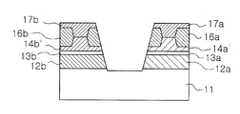
도1a 내지 도1k는 종래의 2파장 반도체 레이저소자의 제조방법을 나타내는 공정설명도이다.1A to 1K are process explanatory diagrams showing a conventional method for manufacturing a two-wavelength semiconductor laser device.
도1a와 같이, n형 GaAs기판(11) 상에 780㎚파장광을 위한 제1 반도체 레이저 에피택셜층을 형성한다. 즉, n형 AlGaAs 클래드층(12a), AlGaAs 활성층(13a) 및 p 형 AlGaAs 클래드층(14a)을 순차적으로 성장시킨다.As shown in FIG. 1A, a first semiconductor laser epitaxial layer for 780 nm wavelength light is formed on an n-
이어, 도1b와 같이, 포토리소그래피공정과 에칭공정을 이용하여 상기 에피택셜층(12a,13a,14a)을 선택적으로 제거하여 GaAs 기판(11) 상면의 일영역을 노출시킨다.1B, the
다음으로, 도1c와 같이, 노출된 GaAs기판(11) 상면에 650㎚파장광을 위한 제2 반도체 레이저 에피택셜층을 형성한다. 즉, n형 AlGaInP 클래드층(12b), GaInP/AlGaInP 활성층(13b) 및 p형 AlGaInP 클래드층(14b)을 순차적으로 성장시킨다.Next, as shown in FIG. 1C, a second semiconductor laser epitaxial layer for 650 nm wavelength light is formed on the exposed
이어, 도1d와 같이, 포토리소그래피공정과 에칭공정을 이용하여, 상기 제1 반도체 레이저 에피택셜층(12a,13a,14a) 위에 제2 반도체 레이저 에피택셜층(12b,13b,14b)을 제거하는 동시에, 2개의 에피택셜구조를 서로 분리시킨다.Subsequently, as shown in FIG. 1D, the second semiconductor laser
다음으로, 도1e와 같이, 상기 p형 AlGaAs 클래드층(14'a)과 상기 p형 AlGaInP 클래드층(14'b)을 통상의 방법으로 선택적으로 에칭하여 전류주입효율향상을 위한 리지구조를 형성한 후에, 도1f와 같이 n형 GaAs 전류제한층(16a,16b)과 p형 GaAs콘택층(17a,17b)을 형성한다.Next, as shown in FIG. 1E, the p-type AlGaAs cladding layer 14'a and the p-type AlGaInP cladding layer 14'b are selectively etched by a conventional method to form a ridge structure for improving current injection efficiency. After that, as shown in Fig. 1F, n-type GaAs current limiting
끝으로, 도1g와 같이 Ti, Pt, Au 또는 그 합금을 이용하여 p형 GaAs콘택층(17a,17b) 상에 p측 전극(19a,19b)을 형성하고, Au/Ge, Au, Ni 또는 그 합금을 이용하여 GaAs기판(11) 하면에 n측 전극(18)을 형성함으로써 2파장 반도체 레이저(10)를 제조할 수 있다.Finally, p-
이와 같이, 2개의 서로 다른 파장의 반도체 레이저(10)를 동일 기판(11) 상에 형성하여 하나의 칩으로 집적화시킬 수 있다. 따라서, 각 반도체 레이저를 별도를 제조한 후에 동일기판 상에 다이본딩방식으로 결합시키는 방식에 비해, 별도의 제조공정과 추가적인 본딩공정을 생략할 수 있어 공정을 간소화할 수 있을 뿐만 아니라, 칩 다이본딩시에 야기될 수 있는 정렬불량문제를 해결할 수 있다.As such, two
하지만, 도1에서 설명된, 종래의 다파장 반도체 레이저제조방법은 2파장(650㎚ 및 780㎚) 반도체 레이저를 위한 제조방법으로만 제한적으로 사용되고 있을 뿐이며, 보다 단파장광을 추가한 3파장 반도체 레이저 제조방법으로서 적용될 수 없다. 대표적으로, 적,녹,청색광을 각각 발진하는 다파장 반도체 레이저를 제조하기 위해서는, 460㎚파장광과 530㎚파장광을 위해 질화물계 에피택셜층으로 구성된 2개의 레이저와, 635㎚파장광을 위해 AlGaInP계 에피택셜층으로 구성된 레이저를 포함한 레이저 구조가 요구된다. 특히, 460㎚파장 및 530㎚파장을 위한 반도체 레이저를 제조하기 위해서는 GaN계 에피택셜층이 요구되므로, 635㎚를 위한 반도체레이저와 동일한 기판에서 형성될 수 없다는 문제가 있다.However, the conventional multi-wavelength semiconductor laser manufacturing method described in FIG. 1 is used only as a manufacturing method for two-wavelength (650 nm and 780 nm) semiconductor lasers, and a three-wavelength semiconductor laser having shorter wavelength light added thereto. It cannot be applied as a manufacturing method. Typically, to manufacture a multi-wavelength semiconductor laser that oscillates red, green, and blue light, respectively, two lasers composed of a nitride-based epitaxial layer for 460 nm wavelength light and 530 nm wavelength light, and for 635 nm wavelength light There is a need for a laser structure including a laser composed of an AlGaInP-based epitaxial layer. In particular, since GaN-based epitaxial layers are required to manufacture semiconductor lasers for 460 nm wavelength and 530 nm wavelength, they cannot be formed on the same substrate as the semiconductor laser for 635 nm.
보다 구체적으로, 635㎚ 반도체 레이저를 위한 AlGaInP 에피택셜층은 격자상수(약 5.6Å)는 GaN 에피택셜층의 격자상수(약 3.2Å)와 큰 차이를 가지므로, 동일한 기판 상에 성장하기 어렵다. AlGaInP 에피택셜층의 경우에는 GaAs기판에 우수한 결정성으로 형성될 수 있으며, GaN 에피택셜층은 동종기판인 GaN기판, 사파이어기판, SiC기판 등과 같이 고유한 질화물 반도체 성장용 기판에 한하여 우수한 결정성 으로 형성될 수 있다. 따라서, 실질적으로 종래의 2파장 반도체 레이저 제조방법을 기초하여, 460㎚, 530㎚ 및 635㎚파장과 같은 삼색광을 발진하는 다파장 반도체 레이저를 제조하는 것이 불가능하다.More specifically, the AlGaInP epitaxial layer for a 635 nm semiconductor laser has a large difference in lattice constant (about 5.6 μs) from that of the GaN epitaxial layer, so it is difficult to grow on the same substrate. The AlGaInP epitaxial layer can be formed with excellent crystallinity on the GaAs substrate, and the GaN epitaxial layer has excellent crystallinity only for intrinsic nitride semiconductor growth substrates such as GaN substrate, sapphire substrate, SiC substrate, etc. Can be formed. Therefore, based on the conventional two-wavelength semiconductor laser manufacturing method, it is impossible to manufacture a multi-wavelength semiconductor laser that oscillates tricolor light such as 460 nm, 530 nm and 635 nm wavelengths.
본 발명은 상기한 종래 기술의 문제를 해결하기 위한 것으로서, 그 목적은 GaN 에피택셜층을 다른 기판에 성장시킨 후에, 분리 및 접합공정을 이용하여 3파장광을 출력할 수 있는 다파장 반도체 레이저의 제조방법을 제공하는데 있다.
SUMMARY OF THE INVENTION The present invention has been made to solve the above-mentioned problems of the prior art, and an object thereof is to grow a GaN epitaxial layer on another substrate, and then to generate a three wavelength light using a separation and bonding process. It is to provide a manufacturing method.
또한, 본 발명의 다른 목적은 상기 다파장 반도체 레이저의 제조방법으로 제조될 수 있는 새로운 구조를 갖는 다파장 반도체 레이저를 제공하는데 있다.
In addition, another object of the present invention is to provide a multi-wavelength semiconductor laser having a novel structure that can be produced by the method for manufacturing a multi-wavelength semiconductor laser.
상기한 기술적 과제를 달성하기 위해서, 본 발명은,In order to achieve the above technical problem, the present invention,
질화물 단결정 성장을 위한 기판을 마련하는 단계와, 상기 질화물 단결정 성장용 기판 상에 제1 도전형 제1 클래드층, 제1 활성층 및 제2 도전형 제1 클래드층으로 순차적으로 성장시켜 제1 질화물 에피택셜층을 형성하는 단계와, 상기 질화물 단결정 성장용 기판의 일영역이 노출되도록 상기 제1 질화물 에피택셜층을 선택적으로 제거하는 단계와, 상기 질화물 단결정 성장용 기판의 노출된 상면에 상기 제1 도전형 제2 클래드층, 제2 활성층 및 제2 도전형 제2 클래드층이 순차적으로 성장 시켜 제2 질화물 에피택셜층을 형성하는 단계와, 상기 질화물 단결정 성장용 기판으로부터 상기 제1 및 제2 질화물 에피택셜층을 분리하는 단계와, 상기 제1 및 제2 질화물 에피택셜층을 제1 도전형 기판 상에 접합시키는 단계와, 상기 제1 및 제2 질화물 반도체 에피택셜층을 선택적으로 에칭하여, 상기 제1 도전형 기판의 일영역이 노출되고, 상기 제1 및 제2 질화물 에피택셜층으로부터 서로 분리된 상기 제1 및 제2 반도체 레이저 구조를 형성하는 단계와, 상기 제1 도전형 기판의 노출된 일영역에 제1 도전형 제3 클래드층, 제3 활성층 및 제2 도전형 제3 클래드층이 순차적으로 성장된 제3 반도체 레이저 구조를 형성하는 단계와, 상기 제1 도전형 기판의 하면과 상기 제1 내지 제3 반도체 레이저구조의 각 제2 도전형 클래드층에 접속되는 제1 및 제2 전극을 형성하는 단계를 포함하는 다파장 반도체 레이저 제조방법을 제공한다.Preparing a substrate for nitride single crystal growth, and sequentially growing a first conductivity type first clad layer, a first active layer, and a second conductivity type first clad layer on the nitride single crystal growth substrate; Forming a tactile layer, selectively removing the first nitride epitaxial layer to expose a region of the nitride single crystal growth substrate, and exposing the first conductive layer on an exposed top surface of the nitride single crystal growth substrate Growing a second cladding layer, a second active layer, and a second conductive second cladding layer sequentially to form a second nitride epitaxial layer; and the first and second nitride epitaxial layers from the nitride single crystal growth substrate. Separating the tactile layer, bonding the first and second nitride epitaxial layers onto a first conductivity type substrate, and the first and second nitride semiconductor epitaxial layers Selectively etching to form the first and second semiconductor laser structures that expose a region of the first conductivity type substrate and are separated from each other from the first and second nitride epitaxial layers; Forming a third semiconductor laser structure in which a first conductive third cladding layer, a third active layer, and a second conductive third cladding layer are sequentially grown in one exposed region of the first conductive substrate; It provides a method of manufacturing a multi-wavelength semiconductor laser comprising the step of forming the first and second electrodes connected to the lower surface of the conductive substrate and each second conductive cladding layer of the first to third semiconductor laser structure.
본 발명의 바람직한 실시형태에서는, 상기 제3 반도체 레이저 구조를 형성하는 단계 후, 상기 제1 및 제2 전극을 형성하는 단계 전에, 상기 제1 내지 제3 반도체 레이저 구조의 각 제2 도전형 클래드층을 선택적으로 에칭하여 리지구조로 형성하는 단계와, 상기 리지구조의 상단면을 제외한 상기 제2 도전형 클래드층 상면에 절연층을 형성하는 단계를 더 포함하며, 이 경우에 상기 제2 전극은 상기 리지구조의 상단면을 통해 각각의 제2 도전형 클래드층에 접속될 수 있다.In a preferred embodiment of the present invention, after forming the third semiconductor laser structure, and before forming the first and second electrodes, each second conductive clad layer of the first to third semiconductor laser structures. Selectively etching to form a ridge structure, and forming an insulating layer on an upper surface of the second conductivity-type cladding layer except for an upper surface of the ridge structure, in which case the second electrode It may be connected to each second conductive cladding layer through the top surface of the ridge structure.
보다 바람직하게는, 상기 절연층은 상기 제1 내지 제3 반도체 레이저의 측면 까지 연장되도록 형성될 수 있으며, 상기 절연층으로는 SiO2 또는 Si3N4일 수 있다.More preferably, the insulating layer may be formed to extend to the side of the first to third semiconductor laser, the insulating layer may be SiO2 or Si3 N4 .
또한, 상기 제1 및 제2 질화물 에피택셜층을 분리하는 단계는, 상기 기판의 하면에 레이저를 조사하여 상기 제1 및 제2 질화물 에피택셜층을 리프트오프시키는 공정으로 실시될 수 있다. 보다 바람직하게는, 상기 레이저를 조사하기 전에 상기 질화물 단결정 성장용 기판의 하면에 대해 래핑을 실시하여 그 두께를 감소시키는 단계를 더 포함할 수 있다.The separating of the first and second nitride epitaxial layers may be performed by a step of lifting off the first and second nitride epitaxial layers by irradiating a laser to a lower surface of the substrate. More preferably, the step of lapping the lower surface of the nitride single crystal growth substrate before irradiating the laser may further comprise the step of reducing the thickness.
나아가, 상기 제1 및 제2 질화물 에피택셜층을 제1 도전형 기판 상에 접합시키는 단계는, 고온에서 상기 제1 및 제2 질화물 에피택셜층을 제1 도전형 기판의 상면에 가압하여 접합시키는 공정으로 실시될 수 있다.Further, the bonding of the first and second nitride epitaxial layers on the first conductivity type substrate may include bonding the first and second nitride epitaxial layers to the upper surface of the first conductivity type substrate at a high temperature. It can be carried out in a process.
상기 제1 질화물 반도체층을 에칭하는 단계에서, 상기 제1 반도체 레이저 구조에 대한 에피택셜층만을 잔류시킬 수 있으며, 상기 제3 반도체 레이저 구조를 형성하는 단계는, 상기 제1 및 제2 반도체 레이저구조가 형성된 상기 제1 도전형 기판의 상면에 제1 도전형 제3 클래드층, 제3 활성층 및 제2 도전형 제3 클래드층을 순차적으로 성장시켜 상기 제3 반도체 레이저를 위한 에피택셜층을 형성하는 단계와, 상기 제3 반도체 레이저를 위한 에피택셜층을 선택적으로 에칭하여, 상기 제1 도전형 기판의 일영역에 상기 제1 및 제2 반도체 레이저 구조와 분리된 제3 반도체 레이저 구조를 형성하는 단계로 구현될 수 있다.In the etching of the first nitride semiconductor layer, only an epitaxial layer with respect to the first semiconductor laser structure may be left, and the forming of the third semiconductor laser structure may include forming the first and second semiconductor laser structures. Forming an epitaxial layer for the third semiconductor laser by sequentially growing a first conductive third cladding layer, a third active layer, and a second conductive third cladding layer on an upper surface of the first conductive type substrate on which the first conductive type substrate is formed. Selectively etching the epitaxial layer for the third semiconductor laser to form a third semiconductor laser structure separate from the first and second semiconductor laser structures in one region of the first conductivity type substrate. It can be implemented as.
또한, 후속 성장공정을 보다 용이하게 위해서, 성장순서대로 제1 및 제3 반도체 레이저를 배치하는 것이 바람직하다. 즉, 상기 제1 내지 제3 반도체 레이저 구조는 상기 제1 도전형 기판의 일측으로부터 순서대로 형성되는 것이 바람직하다.In addition, to facilitate the subsequent growth process, it is preferable to arrange the first and third semiconductor lasers in the order of growth. That is, the first to third semiconductor laser structures are preferably formed in order from one side of the first conductive type substrate.
상기 질화물 단결정 성장용 기판은 사파이어기판, SiC기판 또는 GaN기판일 수 있으며, 상기 제1 질화물 에피택셜층은 청색광을 발진하는 반도체 레이저를 위한 GaN계 반도체물질이며, 상기 제2 질화물 에피택셜층은 녹색광을 발진하는 반도체 레이저를 위한 GaN계 반도체물질일 수 있다.The nitride single crystal growth substrate may be a sapphire substrate, a SiC substrate, or a GaN substrate, and the first nitride epitaxial layer is a GaN-based semiconductor material for a semiconductor laser that emits blue light, and the second nitride epitaxial layer is green light. It may be a GaN-based semiconductor material for the semiconductor laser to oscillate.
또한, 상기 제3 반도체 레이저 구조는 적색광을 발진하기 위해서 AlGaInP계 반도체물질로 구성될 수 있다.In addition, the third semiconductor laser structure may be made of AlGaInP-based semiconductor material in order to emit red light.
나아가, 본 발명은 새로운 구조를 갖는 다파장 반도체 레이저를 제공한다. 상기 다파장 반도체 레이저는, 제1 내지 제3 영역으로 구분되는 상면을 갖는 제1 도전형 기판과, 상기 제1 도전형 기판의 제1 영역 상에 순차적으로 형성된 제1 도전형 제1 GaN계 클래드층, 제1 GaN계 활성층 및 제2 도전형 제1 GaN계 클래드층을 포함한, 청색광을 발진하는 제1 반도체 레이저 구조와, 상기 제1 도전형 기판의 제2 영역 상에 형성된 상기 제1 도전형 제1 GaN계 클래드층, 제2 GaN계 활성층 및 제2 도전형 제2 GaN계 클래드층을 포함한, 녹색광을 발진하는 제2 반도체 레이저 구조와, 상기 제1 도전형 기판의 제3 영역 상에 형성된 상기 제1 도전형 AlGaInP계 클래드층, AlGaInP계 활성층 및 제2 도전형 AlGaInP계 클래드층을 포함한 제3 반도체 레이저 구조와, 상기 제1 도전형 기판의 하면과 상기 제1 내지 제3 반도체 레이저구조의 각 제2 도전형 클래드층에 접속되도록 형성된 제1 및 제2 전극를 포함한다.Furthermore, the present invention provides a multi-wavelength semiconductor laser having a novel structure. The multi-wavelength semiconductor laser may include a first conductivity type substrate having an upper surface divided into first to third regions, and a first conductivity type first GaN cladding sequentially formed on the first region of the first conductivity type substrate. A first semiconductor laser structure that oscillates blue light, including a layer, a first GaN-based active layer, and a second conductivity-type first GaN-based cladding layer, and the first conductivity type formed on a second region of the first conductivity-type substrate. A second semiconductor laser structure for oscillating green light, including a first GaN based cladding layer, a second GaN based active layer, and a second conductive second GaN based cladding layer, and formed on a third region of the first conductive type substrate A third semiconductor laser structure including the first conductivity type AlGaInP cladding layer, an AlGaInP activity layer, and a second conductivity type AlGaInP cladding layer, a lower surface of the first conductivity type substrate, and the first to third semiconductor laser structures To each second conductive cladding layer Rock is formed comprising the first and second jeongeukreul.
본 발명은 성장조건이 다른 에피택셜층으로 구성된 반도체 레이저를 하나의 칩을 구성하기 위해서, 단파장에 해당하는 제1 및 제2 반도체레이저를 위한 질화물 에피택셜층을 형성한 후에, 질화물 에피택셜층을 분리하여 제1 도전형 기판에 접합시키고, 이어 제2 및 제3 반도체 레이저를 형성하는 다파장 반도체 레이저 제조방법을 제공한다. 특히, 본 발명에서는 보다 고온에서 성장되는 질화물 에피택셜층을 먼저 형성한 후에 이를 분리하여 접합함으로써 후속 에피택셜성장공정에 대한 다른 층의 원하지 않는 영향(도펀트의 확산 및 열충격 등)을 감소시키고, 동일기판 상에 각 반도체 레이저 구조를 형성하기 위한 에칭공정이 실시되므로, 각 레이저구조가 보다 정밀하게 정렬된 다파장 반도체 레이저를 제조할 수 있다.According to the present invention, a nitride epitaxial layer is formed after forming a nitride epitaxial layer for the first and second semiconductor lasers corresponding to a short wavelength in order to form a single chip of a semiconductor laser composed of epitaxial layers having different growth conditions. Provided are a multi-wavelength semiconductor laser manufacturing method which is separated and bonded to a first conductive substrate, and then forms second and third semiconductor lasers. In particular, in the present invention, the nitride epitaxial layer grown at a higher temperature is first formed, and then separated and bonded to reduce unwanted effects of other layers (diffusion and thermal shock, etc.) on subsequent epitaxial growth processes, and the same. Since the etching process for forming each semiconductor laser structure on a substrate is performed, it is possible to manufacture a multi-wavelength semiconductor laser in which each laser structure is more precisely aligned.
이하, 첨부된 도면을 참조하여, 본 발명의 바람직한 실시형태를 상세히 설명한다.Hereinafter, preferred embodiments of the present invention will be described in detail with reference to the accompanying drawings.
도2a 내지 도2l는 본 발명의 바람직한 실시형태에 따른 3파장 반도체 레이저의 제조방법을 설명하기 위한 공정단면도이다.2A to 2L are process cross-sectional views for explaining a method for manufacturing a three wavelength semiconductor laser according to a preferred embodiment of the present invention.
우선, 도2a와 같이 사파이어기판(21) 상에 단파장(예, 460㎚) 반도체 레이저 를 위한 제1 질화물 에피택셜층(25a)을 형성한다. 상기 제1 질화물 에피택셜층(25a)은 제1 도전형 제1 클래드층(22a)과, 제1 활성층(23a) 및 제2 도전형 제1 클래드층(24a)을 순차적으로 성장시킴으로써 얻어질 수 있다. 상기 제1 및 제2 도전형 제1 클래드층(22a,24a)은 각각 n형 Al0.1Ga0.9N층과 n형 GaN층 및, p형 Al0.2Ga0.8N층과 p형 GaN층을 구성될 수 있으며, 상기 활성층(23a)은, In0.2Ga0.8N/In0.05Ga0.95N로 구성된 다중양자우물구조로 구성될 수 있다.First, as shown in FIG. 2A, a first
이어, 도2b와 같이, 포토리소그래피공정과 드라이에칭공정을 이용하여, 상기 사파이어기판(21)의 일부상면이 노출되도록, 상기 제1 질화물 에피택셜층(25a)을 선택적으로 에칭한다. 본 에칭공정에서 잔류한 제1 질화물 에피택셜층(25a)은 이에 한정되지는 않으나, 본 실시형태와 같이 제1 반도체 레이저구조(20a)부분만 잔류하도록 제거될 수 있다.Next, as illustrated in FIG. 2B, the first
다음으로, 도2c와 같이 상기 제1 반도체 레이저 구조(20a)가 잔류한 사파이어 기판(21)의 상면에 제2 반도체 레이저구조를 위한 제2 질화물 에피택셜층(25b)을 형성한다. 상기 제2 반도체 레이저를 위한 제2 질화물 에피택셜층(25b)은 제1 도전형 제2 클래드층(22b), 제2 활성층(23b) 및 제2 도전형 제2 클래드층(24b)을 순차적으로 성장시킴으로써 얻어질 수 있다. 상기 제2 질화물 에피택셜층(25b)이 530㎚파장광을 위한 반도체 레이저로 설계될 경우에, 상기 제1 및 제2 도전형 제1 클래드층(22b,24b)은 각각 n형 Al0.1Ga0.9N층과 n형 GaN층 및, p형 Al0.2Ga0.8N층과 p형 GaN층을 구성될 수 있으며, 상기 활성층(23a)은, In0.25Ga0.75N/In0.05Ga0.95N로 구성된 다중양자우물구조로 구성될 수 있다.Next, as shown in FIG. 2C, a second
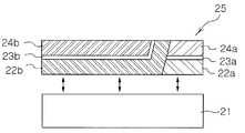
추가적으로, 도2d와 같이 후속될 분리공정 및 접합공정을 용이하게 위해서, 상기 제1 질화물 에피택셜층(25a) 상에 형성된 상기 제2 질화물 에피택셜층(25b)부분을 제거하고 제1 및 제2 질화물 에피택셜층(25a,25b) 상면을 평탄하게 하여 제1 및 제2 반도체 레이저로 제조될 질화물 에피택셜층(25)을 마련할 수 있다.In addition, in order to facilitate a subsequent separation process and a bonding process as shown in FIG. 2D, the portion of the second
또한, 상기 제1 및 제2 질화물 에피택셜층(25a,25b)은 유기금속 화학기상증착(MOCVD) 또는 분자빔에피택시법(MBE)과 같은 공지의 성장방법으로 형성될 수 있다. 상기 사파이어 기판(21)을 대신하여, 동종기판인 GaN기판 또는 SiC기판과 같은 공지된 다른 질화물 반도체 성장용 기판이 사용될 수 있다.In addition, the first and second
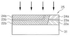
이어, 도2e와 같이, 사파이어기판(21)으로부터 제1 및 제2 질화물 에피택셜층(25)을 분리시킨다. 이러한 분리공정은 레이저를 이용한 리프트오프공정, 드라이에칭법 및, 래핑공정과 같은 공지 방법 또는 그 조합으로 실시될 수 있다. 예를 들어, 레이저를 이용한 리프트오프공정은 5eV이상의 Nd-YAG 레이저를 사파이어 기판(21) 하면에 대해 조사하여 질화물 에피택셜층(25)과 사파이어기판(21)의 계면부근 결정층을 용융시켜 질화물 에피택셜층(25)을 용이하게 리프트오프시킬 수 있 다. 이와 달리, 사파이어 기판(21)에 대해 드라이에칭 또는 래핑공정을 적용하여, 화학적 또는 기계적으로 제거하는 방법을 사용할 수 있으며, 이러한 드라이에칭 또는 래핑공정은 상술된 레이저를 이용한 리프트오프공정과 조합되어 실시될 수 있다. 대표적인 예로서, 래핑공정을 통해 사파이어 기판(21)의 두께를 감소시킨 후에, 레이저를 조사하여 질화물 에피택셜층(25)을 분리하는 공정이 바람직하게 사용될 수 있다.Next, as shown in FIG. 2E, the first and second nitride epitaxial layers 25 are separated from the
다음으로, 도2f와 같이, 분리된 질화물 에피택셜층(25)을 제1 도전형 기판(31) 상에 접합시킨다. 상기 제1 도전형 기판(31)은 후속 성장될 에피택셜층의 성장기판으로서 적합한 n형 GaAs기판일 수 있다. 본 접합공정은 도전성 접착제를 이용할 수 있으나, 바람직하게는 고온에서 소정의 압력으로 가압함으로써 실시될 수도 있다. 예를 들어, 질화물 에피택셜층(25)을 제1 도전형 기판(31)에 배치하고, 약 5㎏/㎠의 압력으로 가압한 채로, 500℃의 온도에서 약 20분간 가열시킴으로써 질화물 에피택셜층(25)과 n형 GaAs기판(31)을 접합시킬 수 있다.Next, as shown in FIG. 2F, the separated
이어, 도2g와 같이, 포토리소그래피과 드라이에칭공정을 이용하여 상기 질화물 에피택셜층(도2e의 25)을 선택적으로 제거함으로써 상기 제1 도전형 기판(31)의 일영역을 노출시키는 동시에, 제1 및 제2 질화물 에피택셜층(25a,25b)로부터 각각 서로 분리된 제1 및 제2 반도체 레이저구조(20a,20b)를 형성한다. 본 공정에서 에칭되어 노출된 제1 도전형 기판(31) 상면은 후속공정에서 제3 반도체 레이저 구조 가 형성될 영역으로서 제공된다.Next, as shown in FIG. 2G, the nitride epitaxial layer (25 of FIG. 2E) is selectively removed by using photolithography and dry etching to expose one region of the first
즉, 상기 제1 도전형 기판(31)의 노출된 상면에 상기 제1 및 제2 반도체 레이저 구조(20a,20b)와 분리되도록, 상기 제1 도전형 제3 클래드층(22c), 제3 활성층(23c) 및 제2 도전형 제3 클래드층(24c)을 순차적으로 성장시킴으로써 제3 반도체 레이저 구조(20c)를 형성한다(도2i 참조). 이러한 제3 반도체 레이저 형성공정은 도2h와 도2i에 걸쳐 예시되어 있다. That is, the first conductive
이하, 도2h 및 도2i를 참조하여 제3 반도체 레이저 형성공정을 설명한다.Hereinafter, a third semiconductor laser forming process will be described with reference to FIGS. 2H and 2I.
다음으로, 도2h와 같이, 상기 제1 및 제2 반도체 레이저 구조(20a,20b)가 형성된 상기 제1 도전형 기판(31)의 상면에 제3 반도체 레이저를 위한 에피택셜층(25c)을 형성한다. 상기 제3 반도체 레이저를 위한 에피택셜층(25c)은 제1 도전형 제3 클래드층(22c), 제3 활성층(23c) 및 제2 도전형 제3 클래드층(24c)을 순차적으로 성장시킴으로써 얻어질 수 있다. 상기 에피택셜층(25c)이 635㎚파장광을 위한 반도체 레이저로 설계되는 경우에, 제1 도전형 및 제2 도전형 제2 클래드층(22c,24c)은 n형 및 p형 (Al0.7Ga0.3)0.5In0.5P층일 수 있으며, 활성층(23c)은 InGaP/(Al0.5Ga0.5)0.5In0.5P층으로 이루어진 다중양자우물구조일 수 있다.Next, as shown in FIG. 2H, an
이어, 도2i와 같이, 상기 제1 도전형 기판(31)의 일영역 중 나머지 일부상면에 제3 반도체 레이저 구조(20c)가 형성되도록, 상기 AlGaInP계 에피택셜층(25c)을 선택적으로 에칭한다. 본 에칭공정에서는 제1 및 제2 반도체 레이저 구조(20a,20b) 의 상면과 각 반도체 레이저구조(20a,20b,20c) 사이에 위치한 AlGaInP계 에피택셜층(25c)을 제거함으로써, 제1 내지 제3 반도체 레이저 구조(20a,20b,20c)를 서로 분리시킨다.Next, as shown in FIG. 2I, the AlGaInP-based
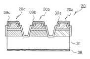
또한, 바람직하게는 도2j와 같이 상기 제1 내지 제3 반도체 레이저 구조(20a,20b,20c)의 각 제2 도전형 클래드층(24a,24b,24c)을 리지구조로 형성하기 위한 에칭공정을 도입할 수 있다. 상기 리지구조의 폭은 약 2∼7㎛을 갖도록 형성될 수 있다. 본 공정을 통해 얻어진 리지구조는 제2 도전형 클래드층(24a,24b,24c)을 통해 주입되는 전류효율을 증가시킬 수 있다.Also, as shown in FIG. 2J, an etching process for forming the second
다음으로, 도2k와 같이, 상기 리지구조의 상단면을 제외한 상기 제2 도전형 클래드층(24a,24b,24c) 상면에 절연층(32)을 형성한다. 상기 절연층(32)은 전류제한층으로서 채용된다. 바람직하게, 상기 절연층(32)은 상기 제1 내지 제3 반도체 레이저 구조(20a,20b,20c)의 측면까지 연장되도록 기판(31) 전면에 대해 형성될 수 있다. 이로써, 상기 절연층(32)은 리지구조를 위한 전류제한층뿐만 아니라, 통상의 페시베이션층으로서 사용될 수도 있다. 이러한 절연층(32)으로는 SiO2 또는 Si3N4가 사용될 수 있다.Next, as shown in FIG. 2K, the insulating
끝으로, 도2l과 같이, 상기 제1 도전형 기판(31)의 하면에 제1 전극(38)을 각각 형성하고, 상기 제1 내지 제3 반도체 레이저구조(20a,20b,20c)의 제2 도전형 클래드층(24a,24b,24c)에 접속되도록 제2 전극(39a,39b,39c)을 각각 형성한다. 본 실시형태와 같이, 상기 제2 전극(39a,39b,39c)은 상기 리지구조의 상단면을 통해 각각의 제2 도전형 클래드층(24a,24b,24c)에 접속되도록 각 반도체 레이저구조(20a,20b,20c)의 상면에 형성될 수 있다. 상기 제1 전극(38)은 AuGe, Au, Ni 또는 그 합금으로 구성될 수 있으며, 상기 제2 전극(39a,39b,39c)은 Ti, Pt, Ni 및 Au로 구성된 그룹으로부터 선택된 적어도 하나의 금속으로 이루어질 수 있다. 이로써, 고유한 파장을 발진하는 3개의 반도체 레이저(20a,20b,20c)를 동일한 기판(31)에 구비한 3파장 반도체 레이저(30)를 제조할 수 있다.Lastly, as shown in FIG. 2L, a
도2l에 도시된 바와 같이, 본 발명을 통해 삼원색(적,녹,청)에 해당하는 3파장광을 발진할 수 있는 반도체 레이저(30)는 제1 도전형 기판(31) 상에 제1 GaN계 물질로 이루어진 제1 반도체 레이저(20a)와, 제2 GaN계 물질로 이루어진 제2 반도체 레이저(20b)와, AlGaIn계 물질로 이루어진 제3 반도체 레이저(20c)를 동시에 집적화시킬 수 있다. 또한, 상기 제1 및 제2 반도체 레이저(20a,20b)는 별도의 질화물 반도체 성장용 기판에서 성장시킨 후에 분리되어 접합되며, 제3 반도체 레이저(20c)의 성장공정을 용이하게 실시하기 위해서, 바람직하게는 제1 도전형 기판(31)의 일측에 배치하며, 나아가 제1 내지 제3 반도체 레이저(20a,20b,20c)도 성장순서에 따라 그 일측으로부터 순서대로 배치하는 것이 바람직하다.As shown in FIG. 2L, the
또한, 리지구조와 전류제한층을 채용하는 경우에, 본 발명에서 각각의 제2 도전형 클래드층(24a,24b,24c)의 절연층(32)으로 구성된 전류제한층을 제공한다. 종래의 역접합을 이용한 전류제한층은 성장조건이 다른 제2 도전형 제1 클래드층(GaN계 물질)이 존재하므로, 3개의 반도체 레이저에 대해 동시에 형성하기 위해서 통상의 절연층(32)을 전류제한층으로서 채용하는 방안을 제공한다. 또한, 상기 절연층은 각 반도체 레이저(20a,20b,20c)의 페시베이션층으로서도 제공되도록 각 반도체 레이저의 측면까지 형성된다.Further, in the case of employing the ridge structure and the current limiting layer, the present invention provides a current limiting layer composed of the insulating
본 발명은 상술한 실시형태 및 첨부된 도면에 의해 한정되는 것이 아니며, 첨부된 청구범위에 의해 한정된다. 따라서, 청구범위에 기재된 본 발명의 기술적 사상을 벗어나지 않는 범위 내에서 다양한 형태의 치환, 변형 및 변경이 가능하다는 것은 당 기술분야의 통상의 지식을 가진 자에게는 자명할 것이며, 이 또한 첨부된 청구범위에 기재된 기술적 사상에 속한다 할 것이다.The present invention is not limited by the above-described embodiment and the accompanying drawings, but by the appended claims. Therefore, it will be apparent to those skilled in the art that various forms of substitution, modification, and alteration are possible without departing from the technical spirit of the present invention described in the claims, and the appended claims. Will belong to the technical spirit described in.
상술한 바와 같이, 본 발명에 따르면, 적녹청색의 파장광의 반도체 레이저 구조를 포함한 다파장 반도체 레이저를 제조하기 위해서 제1 및 제2 GaN계 반도체 레이저를 질화물 반도체성장용 기판에 수평방향으로 나란히 성장시킨 후에 분리시키고, 분리된 반도체층을 다시 GaAs기판과 같은 제1 도전형 기판에 다시 접합하여, 다른 1개의 파장에 해당하는 반도체 레이저구조를 형성함으로써 동일한 기판 상에서 성장될 수 없는 반도체 레이저를 하나의 칩으로 집적화시킬 수 있다.As described above, according to the present invention, in order to manufacture a multi-wavelength semiconductor laser including a semiconductor laser structure of red-green-blue wavelength light, first and second GaN-based semiconductor lasers are grown side by side in a horizontal direction on a nitride semiconductor growth substrate. Later, the semiconductor layer can not be grown on the same substrate by separating and then bonding the separated semiconductor layer back to a first conductive substrate such as a GaAs substrate to form a semiconductor laser structure corresponding to the other wavelength. Can be integrated.
또한, 반도체 레이저를 위한 에피택셜층이 최종 기판에 제공된 상태에서 제조되므로, 완성된 반도체 레이저를 각각 접합시킬 때에 발생되는 정렬불량문제를 해결하는 동시에 보다 간소화된 공정을 통해 우수한 3파장 반도체 레이저를 제조할 수 있다.In addition, since the epitaxial layer for the semiconductor laser is manufactured on the final substrate, an excellent three-wavelength semiconductor laser is manufactured through a simplified process while solving the problem of misalignment caused when bonding the completed semiconductor lasers. can do.
Claims (19)
Translated fromKoreanPriority Applications (4)
| Application Number | Priority Date | Filing Date | Title |
|---|---|---|---|
| KR1020040048079AKR100541110B1 (en) | 2004-06-25 | 2004-06-25 | Multi-wavelength semiconductor laser manufacturing method |
| US10/933,532US20050286591A1 (en) | 2004-06-25 | 2004-09-03 | Method of producing multi-wavelength semiconductor laser device |
| JP2004259659AJP3950878B2 (en) | 2004-06-25 | 2004-09-07 | Multi-wavelength semiconductor laser and manufacturing method thereof |
| US11/857,192US7606280B2 (en) | 2004-06-25 | 2007-09-18 | Method of producing multi-wavelength semiconductor laser device |
Applications Claiming Priority (1)
| Application Number | Priority Date | Filing Date | Title |
|---|---|---|---|
| KR1020040048079AKR100541110B1 (en) | 2004-06-25 | 2004-06-25 | Multi-wavelength semiconductor laser manufacturing method |
Publications (2)
| Publication Number | Publication Date |
|---|---|
| KR20050123423A KR20050123423A (en) | 2005-12-29 |
| KR100541110B1true KR100541110B1 (en) | 2006-01-11 |
Family
ID=35505679
Family Applications (1)
| Application Number | Title | Priority Date | Filing Date |
|---|---|---|---|
| KR1020040048079AExpired - Fee RelatedKR100541110B1 (en) | 2004-06-25 | 2004-06-25 | Multi-wavelength semiconductor laser manufacturing method |
Country Status (3)
| Country | Link |
|---|---|
| US (2) | US20050286591A1 (en) |
| JP (1) | JP3950878B2 (en) |
| KR (1) | KR100541110B1 (en) |
Families Citing this family (54)
| Publication number | Priority date | Publication date | Assignee | Title |
|---|---|---|---|---|
| JP2005347478A (en)* | 2004-06-02 | 2005-12-15 | Sharp Corp | Semiconductor laser element |
| JP2006313875A (en)* | 2005-04-08 | 2006-11-16 | Mitsubishi Electric Corp | Semiconductor laser device |
| US7285968B2 (en)* | 2005-04-19 | 2007-10-23 | Formfactor, Inc. | Apparatus and method for managing thermally induced motion of a probe card assembly |
| US20080304531A1 (en)* | 2007-02-20 | 2008-12-11 | California Institute Of Technology | Integrated broadband quantum cascade laser |
| US9407068B2 (en) | 2007-02-20 | 2016-08-02 | California Institute Of Technology | Integrated broadband quantum cascade laser |
| JP2008235606A (en)* | 2007-03-20 | 2008-10-02 | Sony Corp | Semiconductor light emitting device, method for manufacturing semiconductor light emitting device, backlight, display device, electronic device, and light emitting device |
| KR100856230B1 (en)* | 2007-03-21 | 2008-09-03 | 삼성전기주식회사 | Light emitting device, manufacturing method and monolithic light emitting diode array |
| US8847249B2 (en) | 2008-06-16 | 2014-09-30 | Soraa, Inc. | Solid-state optical device having enhanced indium content in active regions |
| US8767787B1 (en) | 2008-07-14 | 2014-07-01 | Soraa Laser Diode, Inc. | Integrated laser diodes with quality facets on GaN substrates |
| US8805134B1 (en) | 2012-02-17 | 2014-08-12 | Soraa Laser Diode, Inc. | Methods and apparatus for photonic integration in non-polar and semi-polar oriented wave-guided optical devices |
| JP2010166022A (en)* | 2008-09-26 | 2010-07-29 | Sanyo Electric Co Ltd | Semiconductor laser device and display device |
| JP2010166023A (en)* | 2008-09-30 | 2010-07-29 | Sanyo Electric Co Ltd | Semiconductor laser device and display device |
| JP2010109332A (en)* | 2008-09-30 | 2010-05-13 | Sanyo Electric Co Ltd | Semiconductor laser device, and display |
| CN102396083B (en) | 2009-04-13 | 2015-12-16 | 天空激光二极管有限公司 | For the structure of optical means of the use GAN substrate of laser application |
| US8837545B2 (en) | 2009-04-13 | 2014-09-16 | Soraa Laser Diode, Inc. | Optical device structure using GaN substrates and growth structures for laser applications |
| US8634442B1 (en) | 2009-04-13 | 2014-01-21 | Soraa Laser Diode, Inc. | Optical device structure using GaN substrates for laser applications |
| US8427590B2 (en) | 2009-05-29 | 2013-04-23 | Soraa, Inc. | Laser based display method and system |
| US8247887B1 (en) | 2009-05-29 | 2012-08-21 | Soraa, Inc. | Method and surface morphology of non-polar gallium nitride containing substrates |
| US9829780B2 (en) | 2009-05-29 | 2017-11-28 | Soraa Laser Diode, Inc. | Laser light source for a vehicle |
| US9250044B1 (en) | 2009-05-29 | 2016-02-02 | Soraa Laser Diode, Inc. | Gallium and nitrogen containing laser diode dazzling devices and methods of use |
| US10108079B2 (en) | 2009-05-29 | 2018-10-23 | Soraa Laser Diode, Inc. | Laser light source for a vehicle |
| US8750342B1 (en) | 2011-09-09 | 2014-06-10 | Soraa Laser Diode, Inc. | Laser diodes with scribe structures |
| JP5423294B2 (en)* | 2009-09-30 | 2014-02-19 | 住友電気工業株式会社 | Nitride semiconductor light emitting device |
| US8905588B2 (en) | 2010-02-03 | 2014-12-09 | Sorra, Inc. | System and method for providing color light sources in proximity to predetermined wavelength conversion structures |
| US10147850B1 (en) | 2010-02-03 | 2018-12-04 | Soraa, Inc. | System and method for providing color light sources in proximity to predetermined wavelength conversion structures |
| US8451876B1 (en) | 2010-05-17 | 2013-05-28 | Soraa, Inc. | Method and system for providing bidirectional light sources with broad spectrum |
| US20110286484A1 (en)* | 2010-05-24 | 2011-11-24 | Sorra, Inc. | System and Method of Multi-Wavelength Laser Apparatus |
| US8816319B1 (en) | 2010-11-05 | 2014-08-26 | Soraa Laser Diode, Inc. | Method of strain engineering and related optical device using a gallium and nitrogen containing active region |
| US9048170B2 (en) | 2010-11-09 | 2015-06-02 | Soraa Laser Diode, Inc. | Method of fabricating optical devices using laser treatment |
| US9025635B2 (en) | 2011-01-24 | 2015-05-05 | Soraa Laser Diode, Inc. | Laser package having multiple emitters configured on a support member |
| US9595813B2 (en) | 2011-01-24 | 2017-03-14 | Soraa Laser Diode, Inc. | Laser package having multiple emitters configured on a substrate member |
| US9093820B1 (en) | 2011-01-25 | 2015-07-28 | Soraa Laser Diode, Inc. | Method and structure for laser devices using optical blocking regions |
| US9287684B2 (en) | 2011-04-04 | 2016-03-15 | Soraa Laser Diode, Inc. | Laser package having multiple emitters with color wheel |
| US8971370B1 (en) | 2011-10-13 | 2015-03-03 | Soraa Laser Diode, Inc. | Laser devices using a semipolar plane |
| US9020003B1 (en) | 2012-03-14 | 2015-04-28 | Soraa Laser Diode, Inc. | Group III-nitride laser diode grown on a semi-polar orientation of gallium and nitrogen containing substrates |
| US9800016B1 (en) | 2012-04-05 | 2017-10-24 | Soraa Laser Diode, Inc. | Facet on a gallium and nitrogen containing laser diode |
| US9343871B1 (en) | 2012-04-05 | 2016-05-17 | Soraa Laser Diode, Inc. | Facet on a gallium and nitrogen containing laser diode |
| US10559939B1 (en) | 2012-04-05 | 2020-02-11 | Soraa Laser Diode, Inc. | Facet on a gallium and nitrogen containing laser diode |
| US9099843B1 (en) | 2012-07-19 | 2015-08-04 | Soraa Laser Diode, Inc. | High operating temperature laser diodes |
| US8971368B1 (en) | 2012-08-16 | 2015-03-03 | Soraa Laser Diode, Inc. | Laser devices having a gallium and nitrogen containing semipolar surface orientation |
| US10266488B2 (en) | 2013-10-10 | 2019-04-23 | Eastern Virginia Medical School | 4-((2-hydroxy-3-methoxybenzyl)amino)benzenesulfonamide derivatives as potent and selective inhibitors of 12-lipoxygenase |
| US9246311B1 (en) | 2014-11-06 | 2016-01-26 | Soraa Laser Diode, Inc. | Method of manufacture for an ultraviolet laser diode |
| US11437774B2 (en) | 2015-08-19 | 2022-09-06 | Kyocera Sld Laser, Inc. | High-luminous flux laser-based white light source |
| US9787963B2 (en) | 2015-10-08 | 2017-10-10 | Soraa Laser Diode, Inc. | Laser lighting having selective resolution |
| US10771155B2 (en) | 2017-09-28 | 2020-09-08 | Soraa Laser Diode, Inc. | Intelligent visible light with a gallium and nitrogen containing laser source |
| US10222474B1 (en) | 2017-12-13 | 2019-03-05 | Soraa Laser Diode, Inc. | Lidar systems including a gallium and nitrogen containing laser light source |
| US10551728B1 (en) | 2018-04-10 | 2020-02-04 | Soraa Laser Diode, Inc. | Structured phosphors for dynamic lighting |
| GB2579622B (en) | 2018-12-06 | 2021-04-28 | Exalos Ag | Superluminescent diodes and diode modules |
| US11421843B2 (en) | 2018-12-21 | 2022-08-23 | Kyocera Sld Laser, Inc. | Fiber-delivered laser-induced dynamic light system |
| US11239637B2 (en) | 2018-12-21 | 2022-02-01 | Kyocera Sld Laser, Inc. | Fiber delivered laser induced white light system |
| US11884202B2 (en) | 2019-01-18 | 2024-01-30 | Kyocera Sld Laser, Inc. | Laser-based fiber-coupled white light system |
| US12152742B2 (en) | 2019-01-18 | 2024-11-26 | Kyocera Sld Laser, Inc. | Laser-based light guide-coupled wide-spectrum light system |
| US12000552B2 (en) | 2019-01-18 | 2024-06-04 | Kyocera Sld Laser, Inc. | Laser-based fiber-coupled white light system for a vehicle |
| US12191626B1 (en) | 2020-07-31 | 2025-01-07 | Kyocera Sld Laser, Inc. | Vertically emitting laser devices and chip-scale-package laser devices and laser-based, white light emitting devices |
Family Cites Families (31)
| Publication number | Priority date | Publication date | Assignee | Title |
|---|---|---|---|---|
| FR2642228A1 (en)* | 1989-01-20 | 1990-07-27 | Menigaux Louis | METHOD FOR MANUFACTURING A MULTI-WAVELENGTH LASER EFFECT SUSCEPTIBLE LASER EFFECT SEMICONDUCTOR DEVICE AND CORRESPONDING DEVICE |
| JP2809691B2 (en)* | 1989-04-28 | 1998-10-15 | 株式会社東芝 | Semiconductor laser |
| US5436193A (en)* | 1993-11-02 | 1995-07-25 | Xerox Corporation | Method of fabricating a stacked active region laser array |
| US5386428A (en)* | 1993-11-02 | 1995-01-31 | Xerox Corporation | Stacked active region laser array for multicolor emissions |
| US5689123A (en)* | 1994-04-07 | 1997-11-18 | Sdl, Inc. | III-V aresenide-nitride semiconductor materials and devices |
| US5804834A (en)* | 1994-10-28 | 1998-09-08 | Mitsubishi Chemical Corporation | Semiconductor device having contact resistance reducing layer |
| US5777350A (en)* | 1994-12-02 | 1998-07-07 | Nichia Chemical Industries, Ltd. | Nitride semiconductor light-emitting device |
| JPH08307001A (en)* | 1995-04-28 | 1996-11-22 | Mitsubishi Electric Corp | Semiconductor laser diode and method of manufacturing the same |
| JPH09307145A (en) | 1996-05-13 | 1997-11-28 | Nichia Chem Ind Ltd | Optical semiconductor device |
| TW420835B (en)* | 1997-06-16 | 2001-02-01 | Matsushita Electric Industrial Co Ltd | Semiconductor manufacture method and manufacturing device therefor |
| JP3456118B2 (en)* | 1997-07-02 | 2003-10-14 | 松下電器産業株式会社 | Light emitting device, method of manufacturing the same, and optical disk device |
| JP3893735B2 (en) | 1998-04-24 | 2007-03-14 | 松下電器産業株式会社 | Light emitting device |
| US6233265B1 (en)* | 1998-07-31 | 2001-05-15 | Xerox Corporation | AlGaInN LED and laser diode structures for pure blue or green emission |
| US6285698B1 (en)* | 1998-09-25 | 2001-09-04 | Xerox Corporation | MOCVD growth of InGaN quantum well laser structures on a grooved lower waveguiding layer |
| TW498102B (en)* | 1998-12-28 | 2002-08-11 | Futaba Denshi Kogyo Kk | A process for preparing GaN fluorescent substance |
| US20010042866A1 (en)* | 1999-02-05 | 2001-11-22 | Carrie Carter Coman | Inxalygazn optical emitters fabricated via substrate removal |
| JP4024463B2 (en)* | 1999-09-27 | 2007-12-19 | シャープ株式会社 | Manufacturing method of semiconductor light emitting device |
| JP2001184698A (en)* | 1999-12-22 | 2001-07-06 | Pioneer Electronic Corp | Optical pickup device |
| JP3486900B2 (en)* | 2000-02-15 | 2004-01-13 | ソニー株式会社 | Light emitting device and optical device using the same |
| EP1152293A3 (en)* | 2000-05-01 | 2002-10-02 | Fuji Photo Film Co., Ltd. | Image-recording apparatus |
| US6562648B1 (en)* | 2000-08-23 | 2003-05-13 | Xerox Corporation | Structure and method for separation and transfer of semiconductor thin films onto dissimilar substrate materials |
| JP2002118331A (en) | 2000-10-06 | 2002-04-19 | Toshiba Corp | Laminated semiconductor light emitting device and its manufacturing method |
| JP2003015222A (en) | 2001-06-29 | 2003-01-15 | Seiko Epson Corp | Light source device, projector using the same, and mold for reflector for light source device |
| JP3856750B2 (en)* | 2001-11-13 | 2006-12-13 | 松下電器産業株式会社 | Semiconductor device and manufacturing method thereof |
| US6455340B1 (en)* | 2001-12-21 | 2002-09-24 | Xerox Corporation | Method of fabricating GaN semiconductor structures using laser-assisted epitaxial liftoff |
| US20030222263A1 (en)* | 2002-06-04 | 2003-12-04 | Kopin Corporation | High-efficiency light-emitting diodes |
| JP2004014943A (en)* | 2002-06-10 | 2004-01-15 | Sony Corp | Multibeam semiconductor laser, semiconductor light emitting device, and semiconductor device |
| KR20040005269A (en) | 2002-07-09 | 2004-01-16 | 엘지이노텍 주식회사 | Dual-wavelength laser diode and method for fabricating thereof |
| US6759689B2 (en)* | 2002-08-07 | 2004-07-06 | Shin-Etsu Handotai Co., Ltd. | Light emitting element and method for manufacturing the same |
| JP2004304111A (en)* | 2003-04-01 | 2004-10-28 | Sharp Corp | Multi-wavelength laser device |
| KR100631832B1 (en)* | 2003-06-24 | 2006-10-09 | 삼성전기주식회사 | White light emitting device and its manufacturing method |
- 2004
- 2004-06-25KRKR1020040048079Apatent/KR100541110B1/ennot_activeExpired - Fee Related
- 2004-09-03USUS10/933,532patent/US20050286591A1/ennot_activeAbandoned
- 2004-09-07JPJP2004259659Apatent/JP3950878B2/ennot_activeExpired - Fee Related
- 2007
- 2007-09-18USUS11/857,192patent/US7606280B2/ennot_activeExpired - Fee Related
Also Published As
| Publication number | Publication date |
|---|---|
| JP3950878B2 (en) | 2007-08-01 |
| KR20050123423A (en) | 2005-12-29 |
| JP2006013412A (en) | 2006-01-12 |
| US20050286591A1 (en) | 2005-12-29 |
| US7606280B2 (en) | 2009-10-20 |
| US20080009088A1 (en) | 2008-01-10 |
Similar Documents
| Publication | Publication Date | Title |
|---|---|---|
| KR100541110B1 (en) | Multi-wavelength semiconductor laser manufacturing method | |
| US7606281B2 (en) | Method of producing multi-wavelength semiconductor laser device | |
| US8198637B2 (en) | Nitride semiconductor laser and method for fabricating the same | |
| US20090097523A1 (en) | Semiconductor laser apparatus and method of manufacturing the same | |
| JP2008252069A (en) | Method for fabricating semiconductor laser element, and the semiconductor laser element | |
| JP4660224B2 (en) | Semiconductor laser device | |
| JP4015865B2 (en) | Manufacturing method of semiconductor device | |
| JP2007200929A (en) | Manufacturing method of semiconductor light emitting device | |
| JP4847682B2 (en) | Nitride semiconductor device and manufacturing method thereof | |
| JP2001244560A (en) | Semiconductor light emitting device manufacturing method and semiconductor light emitting device | |
| JP2007184644A (en) | Semiconductor device and manufacturing method thereof | |
| JPH10261816A (en) | Semiconductor light emitting device and method of manufacturing the same | |
| KR20060099383A (en) | Laser Diode Chip's Manufacturing Method Of Laser Diode And Laser Diode Chip | |
| KR100674835B1 (en) | Multi-wavelength semiconductor laser manufacturing method | |
| KR100877869B1 (en) | Semiconductor laser diode and manufacturing method thereof | |
| JP2006128675A (en) | Method of manufacturing multiwavelength semiconductor laser | |
| KR100586937B1 (en) | Semiconductor laser device manufacturing method | |
| KR100568323B1 (en) | Multi-wavelength semiconductor laser manufacturing method | |
| JP2008053697A (en) | Method for fabricating semiconductor optical integrated device | |
| JP4839497B2 (en) | Semiconductor light emitting device and method for manufacturing semiconductor light emitting device | |
| JP2011023754A (en) | Semiconductor laser device | |
| JP2011023754A5 (en) | ||
| JP2011018702A (en) | Multi-wavelength semiconductor laser and method of manufacturing the same | |
| JP2011018701A (en) | Multi-wavelength semiconductor laser and method of manufacturing the same |
Legal Events
| Date | Code | Title | Description |
|---|---|---|---|
| A201 | Request for examination | ||
| PA0109 | Patent application | St.27 status event code:A-0-1-A10-A12-nap-PA0109 | |
| PA0201 | Request for examination | St.27 status event code:A-1-2-D10-D11-exm-PA0201 | |
| R18-X000 | Changes to party contact information recorded | St.27 status event code:A-3-3-R10-R18-oth-X000 | |
| D13-X000 | Search requested | St.27 status event code:A-1-2-D10-D13-srh-X000 | |
| D14-X000 | Search report completed | St.27 status event code:A-1-2-D10-D14-srh-X000 | |
| E701 | Decision to grant or registration of patent right | ||
| PE0701 | Decision of registration | St.27 status event code:A-1-2-D10-D22-exm-PE0701 | |
| GRNT | Written decision to grant | ||
| PR0701 | Registration of establishment | St.27 status event code:A-2-4-F10-F11-exm-PR0701 | |
| PG1501 | Laying open of application | St.27 status event code:A-1-1-Q10-Q12-nap-PG1501 | |
| PR1002 | Payment of registration fee | St.27 status event code:A-2-2-U10-U11-oth-PR1002 Fee payment year number:1 | |
| PG1601 | Publication of registration | St.27 status event code:A-4-4-Q10-Q13-nap-PG1601 | |
| R18-X000 | Changes to party contact information recorded | St.27 status event code:A-5-5-R10-R18-oth-X000 | |
| PR1001 | Payment of annual fee | St.27 status event code:A-4-4-U10-U11-oth-PR1001 Fee payment year number:4 | |
| PR1001 | Payment of annual fee | St.27 status event code:A-4-4-U10-U11-oth-PR1001 Fee payment year number:5 | |
| PN2301 | Change of applicant | St.27 status event code:A-5-5-R10-R11-asn-PN2301 | |
| PN2301 | Change of applicant | St.27 status event code:A-5-5-R10-R14-asn-PN2301 | |
| PR1001 | Payment of annual fee | St.27 status event code:A-4-4-U10-U11-oth-PR1001 Fee payment year number:6 | |
| PR1001 | Payment of annual fee | St.27 status event code:A-4-4-U10-U11-oth-PR1001 Fee payment year number:7 | |
| R18-X000 | Changes to party contact information recorded | St.27 status event code:A-5-5-R10-R18-oth-X000 | |
| PN2301 | Change of applicant | St.27 status event code:A-5-5-R10-R11-asn-PN2301 | |
| PN2301 | Change of applicant | St.27 status event code:A-5-5-R10-R14-asn-PN2301 | |
| FPAY | Annual fee payment | Payment date:20121130 Year of fee payment:8 | |
| PR1001 | Payment of annual fee | St.27 status event code:A-4-4-U10-U11-oth-PR1001 Fee payment year number:8 | |
| FPAY | Annual fee payment | Payment date:20131129 Year of fee payment:9 | |
| PR1001 | Payment of annual fee | St.27 status event code:A-4-4-U10-U11-oth-PR1001 Fee payment year number:9 | |
| R18-X000 | Changes to party contact information recorded | St.27 status event code:A-5-5-R10-R18-oth-X000 | |
| LAPS | Lapse due to unpaid annual fee | ||
| PC1903 | Unpaid annual fee | St.27 status event code:A-4-4-U10-U13-oth-PC1903 Not in force date:20141229 Payment event data comment text:Termination Category : DEFAULT_OF_REGISTRATION_FEE | |
| PC1903 | Unpaid annual fee | St.27 status event code:N-4-6-H10-H13-oth-PC1903 Ip right cessation event data comment text:Termination Category : DEFAULT_OF_REGISTRATION_FEE Not in force date:20141229 | |
| R18-X000 | Changes to party contact information recorded | St.27 status event code:A-5-5-R10-R18-oth-X000 |