KR100486994B1 - Integrated circuit device and associated method having openings for exposing integrated circuit dies - Google Patents
Integrated circuit device and associated method having openings for exposing integrated circuit diesDownload PDFInfo
- Publication number
- KR100486994B1 KR100486994B1KR1019970002262AKR19970002262AKR100486994B1KR 100486994 B1KR100486994 B1KR 100486994B1KR 1019970002262 AKR1019970002262 AKR 1019970002262AKR 19970002262 AKR19970002262 AKR 19970002262AKR 100486994 B1KR100486994 B1KR 100486994B1
- Authority
- KR
- South Korea
- Prior art keywords
- integrated circuit
- circuit die
- fingerprint sensor
- opening
- conductive member
- Prior art date
- Legal status (The legal status is an assumption and is not a legal conclusion. Google has not performed a legal analysis and makes no representation as to the accuracy of the status listed.)
- Expired - Lifetime
Links
Images


Classifications
- G—PHYSICS
- G06—COMPUTING OR CALCULATING; COUNTING
- G06V—IMAGE OR VIDEO RECOGNITION OR UNDERSTANDING
- G06V40/00—Recognition of biometric, human-related or animal-related patterns in image or video data
- G06V40/10—Human or animal bodies, e.g. vehicle occupants or pedestrians; Body parts, e.g. hands
- G06V40/12—Fingerprints or palmprints
- G06V40/13—Sensors therefor
- G06V40/1306—Sensors therefor non-optical, e.g. ultrasonic or capacitive sensing
- G—PHYSICS
- G06—COMPUTING OR CALCULATING; COUNTING
- G06F—ELECTRIC DIGITAL DATA PROCESSING
- G06F21/00—Security arrangements for protecting computers, components thereof, programs or data against unauthorised activity
- G06F21/70—Protecting specific internal or peripheral components, in which the protection of a component leads to protection of the entire computer
- G06F21/86—Secure or tamper-resistant housings
- G—PHYSICS
- G06—COMPUTING OR CALCULATING; COUNTING
- G06F—ELECTRIC DIGITAL DATA PROCESSING
- G06F3/00—Input arrangements for transferring data to be processed into a form capable of being handled by the computer; Output arrangements for transferring data from processing unit to output unit, e.g. interface arrangements
- G06F3/01—Input arrangements or combined input and output arrangements for interaction between user and computer
- G06F3/03—Arrangements for converting the position or the displacement of a member into a coded form
- G06F3/041—Digitisers, e.g. for touch screens or touch pads, characterised by the transducing means
- G06F3/044—Digitisers, e.g. for touch screens or touch pads, characterised by the transducing means by capacitive means
- G06F3/0445—Digitisers, e.g. for touch screens or touch pads, characterised by the transducing means by capacitive means using two or more layers of sensing electrodes, e.g. using two layers of electrodes separated by a dielectric layer
- G—PHYSICS
- G06—COMPUTING OR CALCULATING; COUNTING
- G06V—IMAGE OR VIDEO RECOGNITION OR UNDERSTANDING
- G06V40/00—Recognition of biometric, human-related or animal-related patterns in image or video data
- G06V40/10—Human or animal bodies, e.g. vehicle occupants or pedestrians; Body parts, e.g. hands
- G06V40/12—Fingerprints or palmprints
- G—PHYSICS
- G06—COMPUTING OR CALCULATING; COUNTING
- G06V—IMAGE OR VIDEO RECOGNITION OR UNDERSTANDING
- G06V40/00—Recognition of biometric, human-related or animal-related patterns in image or video data
- G06V40/60—Static or dynamic means for assisting the user to position a body part for biometric acquisition
- G06V40/67—Static or dynamic means for assisting the user to position a body part for biometric acquisition by interactive indications to the user
- G—PHYSICS
- G07—CHECKING-DEVICES
- G07C—TIME OR ATTENDANCE REGISTERS; REGISTERING OR INDICATING THE WORKING OF MACHINES; GENERATING RANDOM NUMBERS; VOTING OR LOTTERY APPARATUS; ARRANGEMENTS, SYSTEMS OR APPARATUS FOR CHECKING NOT PROVIDED FOR ELSEWHERE
- G07C9/00—Individual registration on entry or exit
- G07C9/00174—Electronically operated locks; Circuits therefor; Nonmechanical keys therefor, e.g. passive or active electrical keys or other data carriers without mechanical keys
- G07C9/00563—Electronically operated locks; Circuits therefor; Nonmechanical keys therefor, e.g. passive or active electrical keys or other data carriers without mechanical keys using personal physical data of the operator, e.g. finger prints, retinal images, voicepatterns
- G—PHYSICS
- G07—CHECKING-DEVICES
- G07C—TIME OR ATTENDANCE REGISTERS; REGISTERING OR INDICATING THE WORKING OF MACHINES; GENERATING RANDOM NUMBERS; VOTING OR LOTTERY APPARATUS; ARRANGEMENTS, SYSTEMS OR APPARATUS FOR CHECKING NOT PROVIDED FOR ELSEWHERE
- G07C9/00—Individual registration on entry or exit
- G07C9/20—Individual registration on entry or exit involving the use of a pass
- G07C9/22—Individual registration on entry or exit involving the use of a pass in combination with an identity check of the pass holder
- G07C9/25—Individual registration on entry or exit involving the use of a pass in combination with an identity check of the pass holder using biometric data, e.g. fingerprints, iris scans or voice recognition
- G07C9/26—Individual registration on entry or exit involving the use of a pass in combination with an identity check of the pass holder using biometric data, e.g. fingerprints, iris scans or voice recognition using a biometric sensor integrated in the pass
- G—PHYSICS
- G07—CHECKING-DEVICES
- G07C—TIME OR ATTENDANCE REGISTERS; REGISTERING OR INDICATING THE WORKING OF MACHINES; GENERATING RANDOM NUMBERS; VOTING OR LOTTERY APPARATUS; ARRANGEMENTS, SYSTEMS OR APPARATUS FOR CHECKING NOT PROVIDED FOR ELSEWHERE
- G07C9/00—Individual registration on entry or exit
- G07C9/30—Individual registration on entry or exit not involving the use of a pass
- G07C9/32—Individual registration on entry or exit not involving the use of a pass in combination with an identity check
- G07C9/37—Individual registration on entry or exit not involving the use of a pass in combination with an identity check using biometric data, e.g. fingerprints, iris scans or voice recognition
- H—ELECTRICITY
- H01—ELECTRIC ELEMENTS
- H01L—SEMICONDUCTOR DEVICES NOT COVERED BY CLASS H10
- H01L2224/00—Indexing scheme for arrangements for connecting or disconnecting semiconductor or solid-state bodies and methods related thereto as covered by H01L24/00
- H01L2224/01—Means for bonding being attached to, or being formed on, the surface to be connected, e.g. chip-to-package, die-attach, "first-level" interconnects; Manufacturing methods related thereto
- H01L2224/42—Wire connectors; Manufacturing methods related thereto
- H01L2224/47—Structure, shape, material or disposition of the wire connectors after the connecting process
- H01L2224/48—Structure, shape, material or disposition of the wire connectors after the connecting process of an individual wire connector
- H01L2224/4805—Shape
- H01L2224/4809—Loop shape
- H01L2224/48091—Arched
- H—ELECTRICITY
- H01—ELECTRIC ELEMENTS
- H01L—SEMICONDUCTOR DEVICES NOT COVERED BY CLASS H10
- H01L2224/00—Indexing scheme for arrangements for connecting or disconnecting semiconductor or solid-state bodies and methods related thereto as covered by H01L24/00
- H01L2224/01—Means for bonding being attached to, or being formed on, the surface to be connected, e.g. chip-to-package, die-attach, "first-level" interconnects; Manufacturing methods related thereto
- H01L2224/42—Wire connectors; Manufacturing methods related thereto
- H01L2224/47—Structure, shape, material or disposition of the wire connectors after the connecting process
- H01L2224/48—Structure, shape, material or disposition of the wire connectors after the connecting process of an individual wire connector
- H01L2224/481—Disposition
- H01L2224/48151—Connecting between a semiconductor or solid-state body and an item not being a semiconductor or solid-state body, e.g. chip-to-substrate, chip-to-passive
- H01L2224/48221—Connecting between a semiconductor or solid-state body and an item not being a semiconductor or solid-state body, e.g. chip-to-substrate, chip-to-passive the body and the item being stacked
- H01L2224/48245—Connecting between a semiconductor or solid-state body and an item not being a semiconductor or solid-state body, e.g. chip-to-substrate, chip-to-passive the body and the item being stacked the item being metallic
- H01L2224/48247—Connecting between a semiconductor or solid-state body and an item not being a semiconductor or solid-state body, e.g. chip-to-substrate, chip-to-passive the body and the item being stacked the item being metallic connecting the wire to a bond pad of the item
- H—ELECTRICITY
- H01—ELECTRIC ELEMENTS
- H01L—SEMICONDUCTOR DEVICES NOT COVERED BY CLASS H10
- H01L2924/00—Indexing scheme for arrangements or methods for connecting or disconnecting semiconductor or solid-state bodies as covered by H01L24/00
- H01L2924/15—Details of package parts other than the semiconductor or other solid state devices to be connected
- H01L2924/181—Encapsulation
- H01L2924/1815—Shape
- H—ELECTRICITY
- H01—ELECTRIC ELEMENTS
- H01L—SEMICONDUCTOR DEVICES NOT COVERED BY CLASS H10
- H01L2924/00—Indexing scheme for arrangements or methods for connecting or disconnecting semiconductor or solid-state bodies as covered by H01L24/00
- H01L2924/30—Technical effects
- H01L2924/301—Electrical effects
- H01L2924/3011—Impedance
- H—ELECTRICITY
- H01—ELECTRIC ELEMENTS
- H01L—SEMICONDUCTOR DEVICES NOT COVERED BY CLASS H10
- H01L2924/00—Indexing scheme for arrangements or methods for connecting or disconnecting semiconductor or solid-state bodies as covered by H01L24/00
- H01L2924/30—Technical effects
- H01L2924/301—Electrical effects
- H01L2924/3025—Electromagnetic shielding
Landscapes
- Engineering & Computer Science (AREA)
- Theoretical Computer Science (AREA)
- Physics & Mathematics (AREA)
- General Physics & Mathematics (AREA)
- Human Computer Interaction (AREA)
- General Engineering & Computer Science (AREA)
- Multimedia (AREA)
- Computer Hardware Design (AREA)
- Software Systems (AREA)
- Computer Security & Cryptography (AREA)
- Image Input (AREA)
- Measurement Of The Respiration, Hearing Ability, Form, And Blood Characteristics Of Living Organisms (AREA)
- Measurement Of Length, Angles, Or The Like Using Electric Or Magnetic Means (AREA)
- Storage Device Security (AREA)
- Fire-Detection Mechanisms (AREA)
- Electric Clocks (AREA)
- Collating Specific Patterns (AREA)
Abstract
Translated fromKoreanDescription
Translated fromKorean본 발명은 반도체분야와 관련된 것으로서, 상세하게는 집적회로 장치 및 그것을 위한 패키지에 관한 것이다.TECHNICAL FIELD The present invention relates to the field of semiconductors, and more particularly, to an integrated circuit device and a package therefor.
인간이나 인간의 일부분과 직접적인 접근이 가능하게 하는 것과 같이, 몇 가지 응용예에서는 집적회로 다이의 최외부 표면이 환경에 노출되어야 할 것이 요구된다. 예컨대, 혈액 내의 화학물질을 측정하는 것과 같은, 어떤 의학적인 응용예에 있어서는 집적회로를 직접 혈액에 노출시켜 배치한다. 다행스럽게도 그러한 응용예에서는 상기 집적회로의 작동 수명은 한정되어 폐기되기 전까지 단 1회만 사용된다. 따라서, 장기간에 걸친 신뢰성은 통상적으로는 중요한 주제가 아니다.Some applications require that the outermost surface of the integrated circuit die be exposed to the environment, such as allowing direct access to humans or portions of humans. In some medical applications, such as measuring chemicals in the blood, the integrated circuit is directly exposed to the blood and placed. Fortunately, in such applications, the operating life of the integrated circuit is limited and only used once before being discarded. Thus, long term reliability is usually not an important topic.
이에 반하여, 센서소자의 집적회로 배열에 기초하는 지문센서는 집적회로 다이에 손가락이 직접 접촉될 것이 요구될 수 있다. 지문 감지 및 일치는 개인의 신원확인이나 인증을 위한 기술로서 신뢰할 만하며 널리 사용되고 있다.In contrast, a fingerprint sensor based on the integrated circuit arrangement of the sensor element may require that a finger is in direct contact with the integrated circuit die. Fingerprint detection and matching is a reliable and widely used technology for identifying or authenticating individuals.
통상적인 전자 지문센서는 손가락의 표면을 가시광선이나 적외선 또는 초음파 복사에 노출시키는 것에 기초되고 있다. 예컨대, 반사된 에너지는 임의의 카메라 형태에 의하여 잡히고, 그 잡힌 이미지는 조직되고, 디지털화되고 정적인 디지털 이미지로서 저장된다. 미국 특허 제4,210,899호의 명세서에, 임의의 컴퓨터 단말기에의 개인의 접근을 허가하거나 지정하는 것과 같은, 접근보안 응용예를 위하여 중앙처리국과 협력하는 광학주사지문판독기가 개시되어 있다. 미국특허 제4,525,859호의 명세서에는 지문 이미지를 잡기 위한 비디오 카메라를 개시하고 있으며 기준지문의 데이터베이스와의 일치를 결정하기 위하여 지문의 세부, 즉 지문 이랑의 가지들과 단부들의 형태를 이용하고 있다.Conventional electronic fingerprint sensors are based on exposing the surface of a finger to visible, infrared or ultrasonic radiation. For example, the reflected energy is captured by any camera form, and the captured image is organized, digitized and stored as a static digital image. In the specification of US Pat. No. 4,210,899, an optical scanning fingerprint reader is disclosed which cooperates with the central processing station for access security applications, such as granting or assigning individual access to any computer terminal. The specification of US Pat. No. 4,525,859 discloses a video camera for capturing a fingerprint image and uses the details of the fingerprint, ie the branches and ends of the fingerprint gyrus, to determine agreement with the database of the reference fingerprint.
미국특허 제4,353,056호의 명세서에서는 살아있는 지문을 감지하는 다른 방법이 개시되어 있다.In the specification of US Pat. No. 4,353,056, another method for detecting a living fingerprint is disclosed.
미국특허 제5,325,442호의 명세서에서는 복수개의 센서전극을 포함하는 지문센서가 개시되어 있다.In the specification of US Patent No. 5,325,442, a fingerprint sensor including a plurality of sensor electrodes is disclosed.
신원확인 및 인증을 위한 지문 감지 및 일치에 있어서의 큰 진보는 컴퓨터 워크스테이션, 가전제품, 자동차, 및 기밀 자료에 대한 권한 없는 사용을 방지하기 위하여 바람직하다.Major advances in fingerprint detection and matching for identification and authentication are desirable to prevent unauthorized use of computer workstations, consumer electronics, automobiles, and confidential materials.
본 발명의 목적은 사용자의 손가락과 같은 감지된 매체에 의하여 집적회로 다이의 직접적인 접촉을 허락하는 집적회로 장치 및 관련된 방법을 제공하고자 하며, 상기 다이를 위한 신뢰할 수 있는 환경적 밀봉을 제공하고자 하는 것이다.It is an object of the present invention to provide an integrated circuit device and associated method that allows direct contact of an integrated circuit die by a sensed medium, such as a user's finger, and to provide a reliable environmental seal for the die. .
본 발명의 다른 목적은 큰 규모 및 상대적으로 낮은 비용의 제조를 돕는 집적회로 장치 및 관련된 방법을 제공하고자 하는 것이다.It is another object of the present invention to provide an integrated circuit device and associated method that aids in the manufacture of large scale and relatively low cost.
본 발명은 집적회로 장치를 포함하며, 상기 장치는 :The present invention includes an integrated circuit device, the device comprising:
집적회로 다이와;An integrated circuit die;
상기 집적회로 다이를 둘러싸며 상기 집적회로 다이가 노출되도록 하는 열림구를 구비하는 외피물질층; 및An envelope material layer surrounding the integrated circuit die and having an opening for exposing the integrated circuit die; And
상기 열림구에 인접하여 상기 외피물질체에 탑재되는 프레임 부재로 이루어지는 것을 특징으로 한다.And a frame member mounted to the shell material adjacent to the opening.
또한 본 발명은 집적회로 장치를 제조하는 방법을 포함하며, 상기 방법은 :The invention also includes a method of manufacturing an integrated circuit device, the method comprising:
집적회로 다이를 제공하는 단계와;Providing an integrated circuit die;
집적회로 다이 상에 제거가능한 물질체를 배치하는 단계와;Disposing a removable material on the integrated circuit die;
집적회로 다이와 제거 가능한 물질체 주위로 외피물질체를 형성하는 단계; 및Forming an envelope material around the integrated circuit die and the removable material; And
집적회로 다이부를 노출하기 위하여 외피물질체를 통하여 열림구를 결정하는 제거가능한 물질체를 제거하는 단계로 이루어지는 것을 특징으로 한다.Removing the removable material body that determines the opening through the envelope material to expose the integrated circuit die portion.
도전성 부재가 집적회로 다이에 접착하여 부착될 수 있는 이점이 있다. 따라서, 도전성 부재 및 접착제는 다이와 외피물질체 사이의 공간을 밀봉하는 역할을 할 수 있다. 이 도전성 부재는 제조공정의 중간단계에서 제거가능한 물질체를 둘러싸는 프레임으로서 정의될 수 있다. 더욱 상세하게는, 플라스틱이 그 조립제품을 둘러싸게 하도록 사출성형되는 동안에 제거가능한 물질체와 그것의 프레임은 집적회로 상에 배치될 수 있다. 그런 다음 제거가능한 물질체는 제거되고 그럼으로써 외피물질체내에 열림구를 형성하며 둘러싼 외피물질체를 보호하는 도전성 프레임을 남겨둔다. 이 실시예에 있어서는, 도전성 부재가 제조공정 중에 프레임을 정의하며 집적회로 다이의 인접부를 노출하는 열림구의 형성을 편리하게 한다. 도전성 부재는 또한 집적회로 장치의 회로의 한 부분일 수 있다.There is an advantage that the conductive member can be adhered to the integrated circuit die. Thus, the conductive member and the adhesive may serve to seal the space between the die and the envelope material. This conductive member may be defined as a frame surrounding a removable material at an intermediate stage of the manufacturing process. More specifically, the removable material and its frame may be disposed on an integrated circuit while the plastic is injection molded to enclose the assembly. The removable material body is then removed, thereby forming an opening in the shell material, leaving a conductive frame protecting the surrounding shell material. In this embodiment, the conductive member defines a frame during the manufacturing process and facilitates the formation of openings that expose adjacent portions of the integrated circuit die. The conductive member may also be part of a circuit of an integrated circuit device.
집적회로 장치는 도전성 부재를 집적회로 다이에 전기적으로 연결하기 위한 내부연결 수단을 포함하는 것이 바람직하다. 예컨대, 도전성 부재 및 집적회로 사이의 도전성 접착제와, 집적회로 다이 내를 통하여 충전된 적어도 하나의 도체를 포함하는 것이 바람직하다.The integrated circuit device preferably includes internal connecting means for electrically connecting the conductive member to the integrated circuit die. For example, it is preferable to include a conductive adhesive between the conductive member and the integrated circuit and at least one conductor filled through the integrated circuit die.
편리하게는, 본 발명의 지문 센서 실시예에 있어서, 집적회로 다이는 전기장 지문센서를 구성할 수 있다. 더욱 상세하게는, 전기장 지문센서는 전기장 센서전극, 전기장 센서전극과 인접하는 유전체층, 및 전기장 센서전극이 지문 이미지 신호를 생성할 수 있도록 하기 위하여 손가락 주변부와 전기장 센서전극으로 전기장 구동 신호를 인가하는 구동 수단으로 구성되는 것이 바람직하다. 따라서, 도전성 부재는 지문센서부의 전극으로서 작동할 수 있다.Conveniently, in the fingerprint sensor embodiment of the present invention, the integrated circuit die may constitute an electric field fingerprint sensor. More specifically, the electric field fingerprint sensor is configured to apply an electric field driving signal to the finger periphery and the electric field sensor electrode to enable the electric field sensor electrode, the dielectric layer adjacent to the electric field sensor electrode, and the electric field sensor electrode to generate a fingerprint image signal. It is preferable that it is comprised by a means. Thus, the conductive member can operate as an electrode of the fingerprint sensor portion.
본 발명의 다른 양태는 지문을 감지하기 위한 것과 같이, 집적회로 장치를 사용자가 접촉하는 것에 기초하고 있다. 도전성 부재가 사용자의 손가락에 접촉되기 때문에, 정전기적 증대를 제거하기 위하여 그곳의 전압을 고정하기 위하여 도전성 부재에 전압 고정수단이 효과적으로 연결되는 것이 바람직한데, 그럼으로써 집적회로 장치를 정전기적인 방전 손상으로부터 보호하며 및/또는 사용자를 집적회로와의 접촉시 일어날 수 있는 전기적 쇼크로부터 보호하게 된다.Another aspect of the invention is based on a user contacting an integrated circuit device, such as for sensing a fingerprint. Since the conductive member is in contact with the user's finger, it is desirable that the voltage fixing means be effectively connected to the conductive member to fix the voltage therein to eliminate the electrostatic increase, thereby preventing the integrated circuit device from electrostatic discharge damage. And / or to protect the user from electrical shock that may occur upon contact with the integrated circuit.
특히, 집적회로 다이는 복수개의 결합 패드를 추가로 포함하는 것이 바람직하다. 따라서, 외피물질체는 상기 복수개의 결합 패드를 덮는 것이 바람직하다. 또한, 복수개의 결합 패드의 부식을 방지하기 위하여 결합 패드 밀봉수단이 제공될 수 있다. 각 결합 패드는 예컨대 알루미늄으로 구성되는 제 1 금속층을 포함할 수 있다. 따라서, 결합 패드 밀봉수단은 제 1 금속층 상에 차단 금속층을 포함할 수 있다. 결합 패드 밀봉수단은 상기 차단 금속층 상에 금박을 추가로 구비할 수 있다. 결합 패드 밀봉수단은 프레임을 제공하며 다이와의 간격을 밀봉하는 도전성 부재와 함께 사용될 수 있다. 다른 식으로, 몇몇 실시예에 있어서는 결합 패드 밀봉수단은 도전성 부재 또는 프레임 부재없이 사용될 수 있다.In particular, the integrated circuit die preferably further comprises a plurality of coupling pads. Therefore, the outer shell material preferably covers the plurality of bonding pads. In addition, bonding pad sealing means may be provided to prevent corrosion of the plurality of bonding pads. Each bond pad may comprise a first metal layer composed of aluminum, for example. Thus, the bond pad sealing means may comprise a barrier metal layer on the first metal layer. Bonding pad sealing means may further comprise a gold foil on the blocking metal layer. The bond pad seal can be used with a conductive member that provides a frame and seals the gap with the die. Alternatively, in some embodiments, the bond pad sealing means may be used without the conductive member or the frame member.
적절하게는, 외피물질층은 사출성형된 플라스틱으로 구성되는 것이 바람직하다. 도전성 부재 혹은 프레임 부재 및 외피물질층 사이의 간격에서 기계적인 자물쇠를 형성하기 위하여 폐쇄수단이 정의되는 것이 바람직하다. 집적회로의 적절한 수명의 끝을 지시함에 의한 것과 같이 신뢰성을 확신하기 위한 추가 뒷받침을 하기 위하여 집적회로 다이에 부식 감지수단이 연결될 수 있다. 또한, 도전성 부재는 예컨대, 금과 같은 금속으로 구성될 수 있다. 집적회로 다이는 예컨대 질화물, 탄화물 또는 다이아몬드 중의 최소한 하나로 구성되는 강인한 최외각 패시베이션층을 구비하는 것이 바람직하다.Suitably, the skin material layer preferably consists of injection molded plastic. Preferably, closure means are defined to form a mechanical lock at the gap between the conductive member or frame member and the layer of sheath material. Corrosion sensing means can be connected to the integrated circuit die to provide additional support to ensure reliability, such as by indicating the end of the proper life of the integrated circuit. Further, the conductive member may be made of a metal such as gold, for example. The integrated circuit die preferably has a strong outermost passivation layer, for example composed of at least one of nitride, carbide or diamond.
본 발명의 다른 양태에 있어서는, 집적회로 다이는 실리콘 기판과 같이 상대적으로 단단한 기판과, 기판상의 복수개의 금속층을 구비할 수 있다. 다이가 통상적으로 사용자에 의하여 접촉되기 때문에, 금속층은 상대적으로 얇고 집적회로에 강도를 더하여 제공할 수 있도록 상대적으로 단단한 것이 바람직하다. 바람직하게는, 복수개의 금속층은 텅스텐, 몰리브덴, 또는 티탄과 같은 내화성 금속으로 구성된다. 다른 면에서, 본 발명의 이 양태에 있어서는, 복수개의 금속층의 각각은 상대적으로 부드러운 알루미늄은 함유하지 않는 것이 바람직하다.In another aspect of the invention, an integrated circuit die may comprise a relatively rigid substrate, such as a silicon substrate, and a plurality of metal layers on the substrate. Since the die is typically contacted by the user, it is desirable that the metal layer is relatively thin and relatively hard to provide added strength to the integrated circuit. Preferably, the plurality of metal layers is composed of a refractory metal such as tungsten, molybdenum, or titanium. In another aspect, in this aspect of the present invention, it is preferable that each of the plurality of metal layers does not contain relatively soft aluminum.
바람직하게는, 본 발명에 의한 방법은 집적회로 장치를 제조하기 위한 것으로서, 상기 방법에는 : 집적회로 다이를 제공하는 단계와; 집적회로 다이 상에 제거가능한 물질체를 배치하는 단계와; 집적회로 다이 및 제거가능한 물질체 주위로 외피물질체를 형성하는 단계; 및 집적회로 다이부를 노출시키기 위하여 외피물질체를 통한 열림구를 정의하기 위하여 제거가능한 물질체를 제거하는 단계가 포함된다. 집적회로 다이는 지문센서와 같은 센서 또는 다른 집적회로 장치일 수 있다.Preferably, the method according to the invention is for manufacturing an integrated circuit device, the method comprising: providing an integrated circuit die; Disposing a removable material on the integrated circuit die; Forming an envelope material around the integrated circuit die and the removable material; And removing the removable material body to define an opening through the envelope material to expose the integrated circuit die portion. The integrated circuit die may be a sensor such as a fingerprint sensor or other integrated circuit device.
이 방법에는 제거가능한 물질체로 프레임 부재를 고정하는 단계가 추가로 포함될 수 있다. 프레임 부재는 도전성 물질로 이루어질 수 있다. 또한, 제거가능한 물질체를 제거하는 단계에는 프레임 부재가 외피물질체를 대체하여 남아있는 동안에 제거가능한 물질체를 제거하는 단계가 포함되는 것이 바람직하다. 제거가능한 물질체를 배치하는 단계에는 집적회로 다이에 프레임 부재를 접착제로 고정하는 단계가 포함되는 것이 바람직하다. 외피물질체를 형성하는 단계에는 제거가능한 물질체 및 집적회로 다이 주위로 플라스틱을 사출성형하는 단계가 포함될 수 있다. 또한, 제거가능한 물질체는 액체에 용해될 수 있는 물질체인 것이 바람직하며, 그것의 제거단계에는 액체용매에 물질체를 노출하는 단계가 포함되는 것이 바람직하다.The method may further comprise securing the frame member with a removable material. The frame member may be made of a conductive material. In addition, the step of removing the removable material preferably includes removing the removable material while the frame member replaces the envelope material. Positioning the removable material preferably includes securing the frame member to an integrated circuit die with an adhesive. Forming the shell material may include injection molding the plastic around the removable material body and the integrated circuit die. In addition, the removable substance is preferably a substance that can be dissolved in a liquid, and the removing thereof preferably includes exposing the substance to a liquid solvent.
본 발명의 양태에 따른 다른 방법은 집적회로 장치를 제조하기 위한 것으로서, 상기 방법에는 : 집적회로 다이를 제공하는 단계와; 몸체와 돌기를 가지며 돌기가 집적회로부에 접촉할 수 있도록 집적회로 상에 바깥쪽으로 연장되는 형태의 주형을 배치하는 단계; 및 상기 주형내에 외피물질을 배치하고 집적회로를 둘러싸는 단계가 포함된다. 또한 상기 방법에는 외피물질체를 통하는 열림구를 정의하고 그럼으로써 집적회로부를 노출하기 위한 돌기를 포함하는 주형을 제거하는 단계가 포함되는 것이 바람직하다.Another method according to an aspect of the present invention is for manufacturing an integrated circuit device, the method comprising: providing an integrated circuit die; Disposing a mold having a body and a protrusion and extending outwardly on the integrated circuit so that the protrusion can contact the integrated circuit portion; And placing the envelope material within the mold and surrounding the integrated circuit. The method also preferably includes the step of defining an opening through the envelope material and thereby removing the mold comprising a protrusion for exposing the integrated circuit portion.
본 발명을 첨부된 도면 및 실시예에 의하여 상세히 설명하면 다음과 같다.Hereinafter, the present invention will be described in detail with reference to the accompanying drawings and examples.
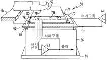
도 1 내지 도 3에 의하여 본 발명에 의한 집적회로 지문센서(30)가 처음으로 기술되어 있다. 예시되어 있는 센서(30)는 하우징(51)과, 손가락이 배치되는 표면을 제공하는 상기 하우징의 상부 표면상에 노출된 유전체층(52) 및 복수개의 신호 전도체(53)를 포함한다. 유전체층(52) 주위로 도전성 스트립 또는 전극(54)이 또한 아래에 상세하게 기술되어질 손가락을 위한 접촉전극을 제공한다. 상기 센서(30)는 상기 하우징 내에 같이 동작하는 처리 수준에 의존하는 정교한 수준의 범위에서 출력신호를 제공할 수 있다.1 to 3, an integrated
지문센서(30)는 개인 신원확인 및 인증목적에 예컨대, 도 1에 도시되어 있는 바와 같이, 자판(36) 및 접을 수 있는 디스플레이 화면(37)을 구비하는 노트북 컴퓨터(35)와 같은 컴퓨터 워크스테이션에의 접근을 허락하는 데에 사용된다. 다시 말해서, 노트북 컴퓨터(37)의 정보 및 프로그램에의 사용자 접근은 요구되는 지문이 먼저 감지되는 경우에만 허락될 수 있다.The
센서(30)는 컴퓨터 정보 시스템(40)을 위한 고정된 워크스테이션(41)에의 접근을 허락 또는 거부하는 데에 사용될 수 있다. 상기 시스템은 근거리 통신망(LAN)(42)에 연동하는 복수개의 워크스테이션(41)을 포함할 수 있는데, 이 LAN은 차례로 지문식별 서버(43) 및 전체적인 중앙 컴퓨터(44)와 연동되어 있다.
도 4 내지 10을 참조하여 지문센서(30)를 설명하면 다음과 같다. 센서(30)는 도 4 및 5에 잘 도시되어 있는 바와 같은 배열 패턴으로 나열된 복수개의 개별 픽셀들 또는 센서소자(30a)들을 포함한다. 본 기술분야의 통상적인 기술자라면 잘 알고 있는 바와 같이, 감지소자들은 도 4에 도시되어 있는 바와 같은 통상적인 지문의 이랑(59)들과 그 사이의 고랑(60)들을 감지할 수 있을 만큼 상대적으로 작다. 본 기술분야의 통상적인 기술자라면 잘 알고 있는 바와 같이, 전기장 센서(30)에서 살아있는 지문 판독은 광학적 판독보다 더 신뢰할 만한데, 이는 이랑과 고랑의 패턴으로 손가락의 피부의 전도는 예컨대, 기판상의 지문이나 혹은 지문의 3차원적인 모델로도 모방하기가 극히 어렵기 때문이다.The
센서(30)는 기판(65)과 그 위에 하나 이상의 활성 반도체층(66)을 포함한다. 예시되어 있는 실시예에 있어서는, 활성 반도체층(66) 위로 절연층(67)을 사이에 두고 접지 평면 전극층(68)이 있다. 그 위로는 다른 절연층(70)을 사이에 두고 구동 전극층(71)이 배치되어 여기 구동 증폭기(74)에 연결되어 있다. 여기 구동신호는 통상적으로 약 1 ㎑ 내지 1 ㎒의 범위일 수 있으며 모든 배열을 통과하여 코히런트하게 전달된다. 따라서, 이렇게 하여 구동 또는 여기 전자장치는 상대적으로 덜 복잡하며 센서(30)의 총비용이 감소될 수 있는 반면에, 신뢰성은 증가된다.
또 다른 절연층(76)이 구동 전극층(71) 위에 배치되고, 예컨대 고리형의 센서전극(78)이 상기 절연층(76) 위에 배치된다. 본 기술분야의 통상적인 기술자라면 쉽게 이해할 수 있는 바와 같이, 센서전극(78)은 도식적으로 예시되어 있는 것과 같이 활성 반도체층(66) 내에 형성되는 센서전자장치(73)에 연결될 수 있다.Another insulating
원형의 차폐 전극(80)이 센서전극(78) 주위의 공간에 둘러싸여 설치된다. 본 기술분야의 통상적인 기술자라면 쉽게 이해할 수 있는 바와 같이, 센서전극(78)과 그 주위의 차폐 전극(80)은 다른 모양으로 만들어질 수 있는데, 예를 들면, 센서소자(30a) 또는 픽셀들의 배열이 최적화되기 쉽도록 육각형으로 될 수도 있다. 차폐 전극(80)은 전기장 에너지의 초점을 돕기 위한 그리고 더 나아가서는 인접 전극을 구동시킬 필요성을 감소시키기 위한 증폭회로(73)의 출력부에 의하여 구동되는 능동적인 차폐장치이다. 따라서, 각각의 센서전극이 개별적으로 구동될 필요가 있는 종래 기술에 의한 센서들과는 아주 다르게, 센서(30)는 모든 센서소자들이 하나의 코히런트한 구동 신호에 의하여 구동될 수 있도록 한다.The
도 8 내지 도 10에 도시되어 있는 바와 같이, 여기 전극(71)은 센서전극(78)으로 제 1 전기장을 발생시키고 센서전극(78) 및 손가락 표면(79) 사이에 제 2 전기장을 각각 d1 및 d2의 거리사이에서 발생시킨다. 다시 말해서, 도 9에 도시되어 있는 바와 같이, 제 1 캐패시터(83)가 여기전극(71)과 센서전극(78) 사이에 설치되며, 제 2 캐패시터(85)가 손가락 표면(79)과 접지점사이에 형성된다. 제 2 캐패시터의 정전용량은 센서전극(78)이 지문의 이랑에 인접하는가 아니면 고랑에 인접하는가에 따라서 변화된다. 따라서, 센서(30)는 용량 분압기라고 생각될 수 있다. 단위 게인 전압 증폭기(73)에 의하여 감지된 전압은 상기 d2 거리가 변화함에 따라서 변화하게 되어 있다.As shown in FIGS. 8 to 10, the
일반적으로, 센서소자(30a)들은 매우 낮은 전류 및 매우 높은 임피던스에서 작동한다. 예컨대, 각 센서전극(78)으로부터의 출력신호는 노이즈에 의한 효과를 줄이고 상기 신호의 후처리작업이 가능하도록 하기 위하여 약 5 내지 10 밀리볼트 정도인 것이 바람직하다. 각 센서소자(30a)의 대략적인 지름은, 차폐 전극(80)의 외부 크기에 의하여 한정되는데, 약 0.002 내지 0.005 인치일 수 있다. 여기 유전층(76) 및 표면 유전층(52)은 약 1 ㎛의 범위내의 두께를 가지는 것이 바람직하다. 접지 평면 전극(68)은 여기 전극(71)으로부터 활성 전자장치들을 차폐한다. 상대적으로 두툼한 유전체층(67)은 이 두 구조 사이의 정전용량을 감소시킴으로써 여기 전극을 구동시키는데 필요한 전류를 감소시키게 된다. 활성 전자 회로들에 전극들(78, 80)을 위하여 다양한 신호 전달체들은 본 기술분야의 기술자들이 이해할 수 있는 바와 같이 쉽게 형성될 수 있다.In general, the
센서(30)에 있어서의 전체 접촉 또는 감지 표면을 약 0.5 × 0.5 인치의 크기로 쉽게 제조할 수 있으면서도 정확한 지문감지 및 식별에 충분한 넓이를 제공하는 크기인 것이 바람직하다. 본 발명에 의한 센서(30)는 또한 죽은 픽셀 또는 센서 소자(30a)들에 대해서도 관대하다. 비록 본 발명에서는 다른 크기의 배열도 생각될 수 있겠으나, 통상적인 센서(30)는 대략 256 × 256 픽셀 또는 센서소자들의 배열을 포함한다. 센서(30)는 또한 기존의 통상적인 반도체 제조기술에 의하여 한 번에 제조될 수 있고 그럼으로써 제조비용을 크게 감소시킬 수 있다.It is desirable that the entire contact or sensing surface in the
도 11에 도시된 바를 참조하여 지문센서(30)의 패키징을 더 설명하면 다음과 같다. 본 기술분야의 통상적인 기술자라면 쉽게 이해할 수 있듯이, 지문센서 집적회로는 스캐닝될 손가락에 의하여 접촉되어야 하는 관계로 그 패키징에는 특별한 어려움이 있다. 통상적인 집적회로의 제조에 있어서는, 부분적으로, 잠재적인 오염가능성 때문에 집적회로에의 접촉은 회피되는 것이 전형적으로 요구되었다. 고려되는 주된 오염물질은 나트륨 및 다른 알칼리 금속들이다. 이러한 이온성 오염물질들은 집적회로를 보호하기 위한 패시베이션에 통상적으로 사용되는 SiO2층내에서 이동성이 매우 크다. 그 결과적인 산화물 전하들은 특히 MOS기술에 있어서 장치의 특성을 저하시킨다.The packaging of the
이동가능한 이온성 오염을 제어하는 통상적인 방법들 중 하나는 집적회로 위로 인이 도프된 패시베이션층과 함께 밀봉 패키징법을 사용한다. 본 기술분야의 통상적인 기술자라면 쉽게 이해할 수 있듯이, 인의 도핑에 의하여 트래핑 메카니즘에 의해 오염물질의 이동성이 저하된다. 근래에는 플라스틱 패키징이 더욱 널리 사용되며 이 플라스틱 패키징과 함께 질화실리콘 또는 탄화시리콘 패시베이션층이 사용될 수 있다. 질화실리콘이나 탄화실리콘의 사용으로 오염물질의 침투성이 크게 감소됨으로써 사용자의 손가락이 집적회로에 직접 접촉될 수 있다. 따라서, 본 발명의 일실시예에 따른 지문센서(30)의 최외각의 패시베이션층으로서 질화실리콘이나 탄화실리콘이 사용되는 것이 바람직하다.One of the conventional methods of controlling movable ionic contamination uses a sealed packaging method with a passivation layer doped with phosphorus over an integrated circuit. As will be readily appreciated by one of ordinary skill in the art, the mobility of contaminants is degraded by the trapping mechanism by the doping of phosphorus. In recent years, plastic packaging is more widely used, and a silicon nitride or silicon carbide passivation layer may be used with the plastic packaging. The use of silicon nitride or silicon carbide greatly reduces the permeability of contaminants, so that the user's finger may be in direct contact with the integrated circuit. Therefore, silicon nitride or silicon carbide is preferably used as the outermost passivation layer of the
또한 지문센서(30)와 같은 집적회로 장치에는 몇 가지 독특한 패키징 요구조건이 제기되는데, 이 요구조건에는 : 패키지가 손가락과 센서 다이 접촉을 가능하게 하도록 열려질 필요가 있는 점과, 패키지는 거친 사용을 견딜 수 있도록 물리적으로 강해야만 하는 점과, 패키지 및 다이는 문지르는 것을 포함하여 세정 및/또는 살균 용액을 사용하는 반복적인 세척에 견딜 수 있어야만 하는 점과, 다이는 넓은 범위의 유기적인 및 비유기적인 다양한 오염물질과의 접촉을 견딜 수 있어야 하고 마멸에도 견딜 수 있어야 하는 점, 및 마지막으로 패키지는 상대적으로 값싼 것이어야 하는 점들이 포함된다.There are also some unique packaging requirements for integrated circuit devices such as the
도 11에 예시되어 있는 패키지(51)는 이러한 패키지 요구를 중점을 두어 다루고 있다. 패키지(51)에는 플라스틱 외피물질체(94)의 사출성형시 리드프레임(93) 위에 마운트되는 집적회로 다이(91)가 포함된다. 연결은 결합 선(97)과 리드프레임(93)을 바깥쪽으로 연장되는 리드(53)에 연결함으로써 될 수 있다. 패키지(51)의 상부 표면에는 다이(91)와의 직접적인 접촉을 가능하게 하는 전체적으로 주조된 열림구(98)가 포함된다. 보다 상세하게는, 예시되어 있는 실시예에 있어서는, 전극(54)으로서 기능하는 프레임 부재 또는 도전성 부재에 의하여 열림구(98)가 정의된다. 예시적으로 아래에서 자세하게 설명되는 바와 같은 센서(30)의 제조에 있어서 이점을 제공하는 도전성 접착제(95)에 의하여 다이(91)의 아랫면에 전극(54)이 연결되어 있다.The
전극(54)의 내부로 노출되는 면은 약간 경사져 있을 수 있다. 프레임 부재 또는 전극(54)은 플라스틱 물질의 돌기와 전극내의 대응하는 홈 사이에 맞물림 접합부에 의하여 외피물질체(94) 내에 배치되어 기계적으로 유지된다. 물론, 외피물질체(94) 및 전극(54) 사이 공간에서 맞물림하는 수단의 다른 방식들은 이 분야의 통상적인 기술자라면 쉽게 생각할 수 있을 것이다.The surface exposed to the inside of the
전극(54)은 집적회로(91)내의 회로에 내적으로 연결되는 것이 이점이 있을 수 있다. 특히 도 12에 도시되어 있는 바를 참조하면, 통로(104')를 통해 충전된 전도체가 전극(54')에 연결하도록 사용될 수 있다. 도 12에 의하여 또한 도시되어 있는 바와 같이, 외피물질체(94')와 전극(54')사이의 간격에서 다른 방식의 기계적인 맞물림 방식이 예시되어 있다. 예시되어 있는 전극(54')은 L-형상의 단면을 가지며 본 기술분야의 통상적인 기술자라면 다른 단면 형태도 가능하고 본 발명에 의하여 고려되고 있다는 것을 쉽게 이해할 수 있을 것이다.It may be advantageous for the
또한, 도 12에 의하여 도시되어 있는 바는 전극(54')이 열림구(98')와 떨어져 설치되어 있는 본 발명의 일실시예다. 보다 상세하게는, 아래에서 자세히 설명하는 바와 같이, 성형 도중에 열림구를 형성하는 제거가능한 물질체를 유지하기 위하여 버팀목(105)이 사용될 수 있다. 다시 말해서, 성형 도중에 프레임 부재 또는 전극(54')와 제거가능한 물질체 사이의 공간을 하나 이상의 버팀목(105)이 정의할 수 있다는 것이다. 따라서, 플라스틱의 내면(91a)은 사출성형 도중 전극(54')의 안쪽으로 형성된다.In addition, the bar shown by FIG. 12 is an embodiment of the present invention in which the electrode 54 'is provided away from the opening 98'. More specifically, as shown in more detail below, shoring 105 may be used to hold a removable material that forms openings during molding. In other words, one or
도 12에 도시되어 있는 것은 전극(54')에서의 전압 고정에 관련되어 있다. 보다 상세하게는, 사용자의 손가락 상의 정전기적인 전압은, 만약 적절하게 흩어버져지지 않는다면, 본 기술분야의 통상적인 기술자라면 쉽게 이해할 수 있듯이, 집적회로 다이(91')의 구성부분에 손상을 줄 수 있다. 또한, 구동 회로(109)로부터 전극(54')으로 인가되는 전압은 우연한 사용자의 쇼크를 회피하기 위하여 소정 수준를 초과하지 않는 것이 바람직하다. 따라서, 본 발명은 예시되어 있는 바와 같이 제너 다이오드 쌍(111) 및 저항(112)에 의하여 제공되는 전압 고정회로(108)를 포함하는 이점을 가진다. 지문센서의 임의의 실시예 혹은 다른 집적회로 장치에 있어서 접지 전극은 필수요소를 아닌데, 몸체 스스로가 지문센서를 위한 커다란 캐패시터로서 기능할 수 있기 때문이다. 그러나, 예시되어 있는 전극(54')은 고정회로(109)와 협력하여 작동하여 정전기적 방전을 흩어버리기 위한 손가락 접촉을 위한 전도체를 제공하는 이점을 가진다. 본 명세서에서 기술되어 있는 바와 같이, 본 발명의 또 다른 실시예에 있어서는, 상기 전극(54)은 최종적인 집적회로 장치내에서 필요하지 않을 수도 있다.Shown in FIG. 12 relates to voltage fixation at
도 13을 참조하여 본 발명의 다른 양태를 설명하면 다음과 같다. 본 발명의 어떤 실시예에 있어서는 추가적인 결합 패드의 보호가 제공된다. 예시된 구조에 있어서는, 예컨대 알루미늄으로 이루어진 결합 패드(120)가 다이의 외부면에 형성된다. 제 1 패시베이션층(122)가 다이의 상부위로 형성되어 결합 패드(120)의 모서리부분을 덥는다. 더 두꺼운 것이 바람직한 제 2 패시베이션층(123)이 제 1 패시베이션층(122) 위에 도포된다. 차단 금속층(124)이 제 2 패시베이션층(123) 내의 열림구 상에 형성되어 아래에 놓인 알루미늄 결합 패드(120)와 접한다. 차단 금속은 아래에 놓인 상대적으로 부식에 민감한 알루미늄을 보호하기 위하여 티탄/텅스텐; 질화 티탄/텅스텐; 및 티탄/텅스템의 영역으로 구성되는 합금일 수 있다. 금층(126)이 차단 금속층(124) 위에 형성될 수 있으며, 본 기술분야의 통상적인 기술자라면 쉽게 이해할 수 있듯이 그리로 결합선(97")이 연결될 수 있다. 또한 물이나 다른 오염원에 노출되는 경우의 부식이나 열화로부터 민감한 결합 패드(120)를 보호하는 다른 유사한 구조에 대하여는 이 기술분야의 통상적인 기술자라면 쉽게 인식할 수 있을 것이다.Another embodiment of the present invention will be described with reference to FIG. 13. In some embodiments of the invention, additional bond pad protection is provided. In the illustrated structure, a
외부 패시베이션층(123)은 위에서 강조된 이유들 때문에 질화실리콘으로 구성될 수 있다. 또한, 마멸 저항 및 물리적인 보호에 장점을 가진 폴리이미드 또는 PTFE(등록상표 '테플론')과 같은 유기물질로 구성되는 다른 보호 코팅이 제공될 수 있다. 탄화실리콘이나 비정질 다이아몬드와 같은 비유기물층도 외부층(123)으로 사용될 수 있는데, 이 경우에는 마멸 저항 특히 연마성 입자들에 대한 저항이 크게 향상될 수 있다. 또한, 외부 패시베이션층(123)의 물질은 예컨대 결합 패드 에칭이 가능하게 되는 표준 IC 패턴 정의 방법과 양립가능한 것이 바람직하다.The
도 13을 참조하면, 집적회로 다이(91")에는 상대적으로 견고한 실리콘 기판(132)에 의하여 지지되는 복수개의 금속층(131)과 그 사이에 낀 유전체층(130)이 포함된다. 통상적으로 어닐된 알루미늄은 전형적으로는 상대적으로 부드러우며 상대적으로 큰 두께로 증착된다. 금속층(131)은 상대적으로 얇으며 상대적으로 견고한 내화 금속 또는 합금에 의하여 제공될 수 있다. 예컨대, 내화 금속에는 텅스텐, 몰리브덴, 티탄 또는 이들의 합금이 포함될 수 있다. 다른 내화 금속 및 비내와금속은 상대적으로 견고하며 상대적으로 얇은 층으로 형성될 수 있는 한 또한 사용될 수 있다. 예컨대, CVD 텅스텐에 있어서 그 두께는 약 0.1 ㎛ 이상이고 약 1.0 ㎛이하인 것이 바람직하다. 다른 식으로 생각하면, 상기 금속층은 알루미늄을 함유하지 않는 것이 바람직하다. 이렇게 하여, 집적회로 다이(91")는 예컨대 사용자의 손가락의 직접적이고 물리적인 접촉으로 야기될 수도 있는 손상에 저항력이 더욱 강하게 된다.13, an integrated circuit die 91 "includes a plurality of
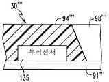
이 기술분야의 통상적인 기술자라면 여기에 기술되어 있으며 도 13에 의하여 도시되어 있는 결합 패드 밀봉수단이 접착제에 의하여 고정되는 전극(54)에 의하여 제공되는 간격 밀봉과 결합하여 사용하면 이점이 있을 것이라는 것을 쉽게 인식할 수 있을 것이다. 도 14에 의하여 도시되어 있는 바와 같은 어떤 실시예에 있어서는 결합 패드 밀봉수단이 단독으로 사용될 수도 있는데, 즉 간격의 전부분이나 그 일부분에 대하여도 열림구(98")에 인접하여 남아있는 전극이 없다. 또한 도 14에 도시된 바와 같이, 결합 패드의 단락이나 다른 구성부품의 손상이 발생하기 전에 부식감지수단(135)이 집적회로 다이(91'") 상의 제어 논리를 가능하게 하거나 원격지에서 부식을 감지할 수 있도록 제공될 수 있다. 부식감지 수단(135)은 이 기술분야의 통상적인 기술자라면 쉽게 이해할 수 있득이 그 값의 변화를 주기적으로 모니터하는 보조네트워크에 의하여 제공될 수 있다.Those skilled in the art will appreciate that the bonding pad sealing means described herein and illustrated by FIG. 13 may be advantageous in combination with the gap sealing provided by the
도 15에 의하여 지문센서(30"")의 다른 변형이 도시되어 있는데, 집적회로 다이는 사용자가 가지고 다니는 카드(139)를 정의하는 플라스틱 물질내에 매몰되어 있다. 예시되어 있는 센서(30"")는 일반적으로 사각형의 열림구 부분을 따라 연장되는 단일 전극부(54"")를 포함할 뿐이다. 위에서 기술한 바와 같은 다른 실시예에 있어서, 전극 또는 프레임 부재는 사각형과 같은 닫힌 기학학적 도형으로 정의될 수 있다. 카드(139)는 예컨대 데이터를 기억하기 위해 예시된 마그네틱 스트립(138)을 포함할 수 있으며, 이 스트립(138)은 이 분야의 통상적인 기술자라면 쉽게 이해할 수 있듯이 지문센서(30"")과 협력하여 작동한다. 카드(139)에는 데이터 처리 및 저장을 가능하게 하는 다른 하나이상의 집적회로 다이가 또한 포함될 수 있다.Another variation of the
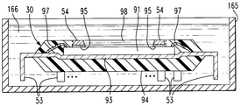
도 16 내지 18을 참조하여 본 발명의 다른 방법의 실시예를 설명하면 다음과 같다. 도 16에 도시된 바와 같이, 전극(54), 제거가능한 물질체(151), 및 전극의 하부상의 접착층(95)을 포함하는 어셈블리(150)가 집적회로 다이(91) 상으로 얼라인 되어 배치되며, 이 다이는 리드 프레임(93)에 연결, 고정된다. 이렇게 형성된 구조는 도 17에 도시된 통상적인 집적회로 패키지 사출 성형기(160)와 외피 플라스틱 물질체(94) 내에 배치된다. 도 18에 도시된 바와 같이, 사출성형기(160)로부터 제거된 후, 상기 구조는 예컨대, 물과 같은 용매(166)가 들어있는 용액조(165) 내에 배치되고 제거가능한 물질체는 용해되어 제거되고 집적회로 다이(91)의 상부에 열림구(98)를 형성한다. 또한, 제거가능한 물질을 용해하기 위하여 용매 스프레이도 사용될 수 있다.An embodiment of another method of the present invention will be described with reference to FIGS. 16 to 18. As shown in FIG. 16, an
도 19 및 20을 참조하여 도 14의 집적회로 장치(30'")를 제조하는 본 발명에 따른 다른 방법을 설명하면 다음과 같다. 본 실시예에 있어서는, 성형기의 상부(171)에는 아래쪽으로 연장되는 몸체(173)와 돌기(172)가 포함된다. 성형기의 상부(171)가 성형기의 하부(174)와 결합되고, 플라스틱 외피물질(94'")이 도 20에 도시된 바와 같이 정의된 성형기 캐비티내로 사출된다. 돌기(172)는 내부에 공동이 형성될 수 있다. 다른 구성요소들은 삼중의 프라임으로 표시되어 있다.Referring to Figs. 19 and 20, another method according to the present invention for manufacturing the integrated circuit device 30 '"of Fig. 14 will be described. In this embodiment, the
이 분야의 통상적인 기술자라면 쉽게 이해할 수 있는 바와 같이, 사출 성형 공정동안에 집적회로 다이(91)에 대하여 돌기(172)를 확실히 바이어스하기 위한 설비가 제공될 수 있다. 주형의 상부와 하부는 집적회로 장치(30'")를 꺼내기 위해 분리될 수 있다.As will be readily appreciated by those skilled in the art, provision may be made for biasing the
본 발명은 특히 사용자의 손가락이 직접 접촉되어 수행되는 지문센서(30)에 응용가능하다. 본 발명은 또한 가스 또는 액체 센서와 같은 다른 센서에도 사용가능한데, 여기서는 감지된 매체에 집적회로 다이의 직접적인 노출이 요구되고 그러한 노출로부터 다이의 다른 부분이 보호될 필요성이 있는 경우이다.The present invention is particularly applicable to the
지문센서(30)및 그와 관련된 처리회로의 다양한 실시예는 많은 통상적인 지문일치 알고리즘 중 어느 것에 있어서도 구현될 수 있다.Various embodiments of
지문의 세부들, 즉 지문 이랑의 가지들이나 혹은 갈라지는 모양 및 끝점들은 종종 샘플지문과 기준지문 데이터베이스 사이의 일치를 결정하기 위하여 사용된다. 그러한 세부 일치는 프로세싱 회로에 의하여 쉽게 구현될 수 있다. 미국특허 제3,859,633호 및 제3,893,080호의 명세서에는 지문의 세부들의 일치에 기초하는 지문식별법이 개시되어 있다. 미국특허 제4,151,512호의 명세서에는 추출된 이랑의 윤곽선 데이터를 사용하는 지문 분류법이 개시되어 있다. 미국특허 제4,185,270호의 명세서에는 세부에 기초하는 변환 및 인증을 위한 방법이 개시되어 있다. 미국특허 제5,040,224호의 명세서에는 세부 패턴에 의한 나중의 일치확인을 위하여 각 지문 이미지의 중심 위치를 바르게 결정하기 위한 지문처리방법이 개시되어 있다.The details of the fingerprint, ie the branches of the fingerprint ridge or the shape and endpoints of the fingerprint, are often used to determine the correspondence between the sample fingerprint and the reference fingerprint database. Such detail matching can be easily implemented by the processing circuit. The specification of US Pat. Nos. 3,859,633 and 3,893,080 discloses a fingerprint identification method based on matching of details of a fingerprint. The specification of US Pat. No. 4,151,512 discloses a fingerprint classification method using contour data of extracted ridges. The specification of US Pat. No. 4,185,270 discloses a method for conversion and authentication based on details. The specification of US Pat. No. 5,040,224 discloses a fingerprint processing method for correctly determining the center position of each fingerprint image for later confirmation of conformity by detailed pattern.
상기한 바와 같이 본 발명은 지문센서 장치를 포함하며, 집적회로 다이와, 집적회로 다이를 둘러싸며 집적회로 다이 부분을 노출시키는 열림구를 가지는 외피물질체, 그리고 열림구에 인접하여 외피물질체에 마운트되는 도전성 부재 또는 프레임을 구비하는 집적회로 장치에 관한 것이다. 도전성 부재는 집적회로 다이에 접착되어 부착된다. 따라서, 접착되어 설치되는 도전성 부재는 외피층 및 다이 사이의 공간을 밀봉하는 역할을 할 수 있다. 프레임은 제조공정의 중간 단계에서 제거가능한 물질을 둘러싸는 것으로 정의될 수 있다. 제거 가능한 물질층 및 그것의 프레임은 플라스틱이 사출되어 어셈블리를 둘러싸게 하기 위해 주조되는 동안에 집적회로 다이 상에 설치될 수 있다.As described above, the present invention includes a fingerprint sensor device, and includes an integrated circuit die, an envelope material surrounding the integrated circuit die and having an opening for exposing the integrated circuit die portion, and mounted to the envelope material adjacent to the opening. An integrated circuit device having a conductive member or frame. The conductive member is adhered to and attached to the integrated circuit die. Therefore, the conductive member bonded and installed may serve to seal the space between the outer skin layer and the die. The frame can be defined as surrounding the removable material at an intermediate stage of the manufacturing process. The removable material layer and its frame may be installed on an integrated circuit die while plastic is cast to inject and surround the assembly.
도 1은 노트북 컴퓨터와 결합되어 있는 상태인 집적회로 지문센서를 도시하고 있는 개략도.1 is a schematic diagram illustrating an integrated circuit fingerprint sensor in a state coupled with a notebook computer.
도 2는 컴퓨터 워크스테이션 및 관련 정보처리 컴퓨터 그리고 근거리통신망(LAN)과 결합되어 있는 상태의 집적회로 지문센서를 도시하고 있는 개략도.2 is a schematic diagram showing an integrated circuit fingerprint sensor in a state coupled with a computer workstation and associated information processing computer and a local area network (LAN).
도 3은 집적회로 지문센서의 일실시예에 대한 도식적인 원근 조감도.3 is a schematic perspective view of one embodiment of an integrated circuit fingerprint sensor.
도 4는 집적회로 지문센서부 및 그 위에 있는 지문 패턴이 명확한 예시를 위해 크게 확대된 상태로 도시되어 있는 평면도.4 is a plan view showing the integrated circuit fingerprint sensor unit and the fingerprint pattern thereon in a greatly enlarged state for clarity of illustration.
도 5는 집적회로 지문센서부의 상부 유전체층이 제거된 모습이 명확한 예시를 위해 크게 확대된 상태로 도시되어 있는 평면도.FIG. 5 is a plan view showing an enlarged state in which the upper dielectric layer of the integrated circuit fingerprint sensor unit is removed for clarity.
도 6은 집적회로 지문센서부에 대한 도식적인 원근 조감도.6 is a schematic perspective view of the integrated circuit fingerprint sensor.
도 7은 집적회로 지문센서부에 대한 도식적인 부분도.7 is a schematic partial view of an integrated circuit fingerprint sensor.
도 8은 전기장이 표시되어 있는 부분적인 단면의 도시적인 측면도.8 is an illustrative side view of a partial cross section in which an electric field is indicated;
도 9는 지문센서부의 도식적인 회로도.9 is a schematic circuit diagram of a fingerprint sensor unit.
도 10은 전기장이 표시되어 있는 부분적인 단면의 확대된 도식적인 측면도.10 is an enlarged schematic side view of a partial cross section showing an electric field;
도 11은 도 3의 11-11 선을 따라 자른 단면을 약간 확대한 도식적인 개략도.FIG. 11 is a schematic enlarged view of a section cut along the line 11-11 of FIG. 3; FIG.
도 12는 집적회로 장치의 다른 실시예의 단면을 크게 확대한 도식적인 개략도.12 is a schematic schematic enlarged view of a cross section of another embodiment of an integrated circuit device.
도 13은 집적회로 장치의 다른 실시예의 접촉 패드에 대한 단면을 크게 확대한 도식적인 개략도.FIG. 13 is a schematic enlarged enlarged cross section of a contact pad of another embodiment of an integrated circuit device. FIG.
도 14는 집적회로 장치의 다른 실시예의 단면을 크게 확대한 도식적인 개략도.14 is a schematic schematic enlarged view of a cross section of another embodiment of an integrated circuit device.
도 15는 들고다니는 카드내에 결합되어 있는 집적회로 지문감지장치의 평면도.Fig. 15 is a plan view of an integrated circuit fingerprint sensing device coupled within a carrying card.
도 16 내지 도 18은 제공공정 중의 집적회로 장치의 단면의 도식도.16 to 18 are schematic views of a cross section of an integrated circuit device during a provision process.
도 19 및 도 20은 다른 제조공정 중의 집적회로 장치의 단면의 도식도.19 and 20 are schematic views of a cross section of an integrated circuit device during another manufacturing process.
Claims (14)
Translated fromKoreanApplications Claiming Priority (4)
| Application Number | Priority Date | Filing Date | Title |
|---|---|---|---|
| US08/592,472 | 1996-01-26 | ||
| US08/592,472US5956415A (en) | 1996-01-26 | 1996-01-26 | Enhanced security fingerprint sensor package and related methods |
| US08/671,430 | 1996-06-27 | ||
| US08/671,430US5862248A (en) | 1996-01-26 | 1996-06-27 | Integrated circuit device having an opening exposing the integrated circuit die and related methods |
Publications (2)
| Publication Number | Publication Date |
|---|---|
| KR980006151A KR980006151A (en) | 1998-03-30 |
| KR100486994B1true KR100486994B1 (en) | 2005-08-05 |
Family
ID=24370781
Family Applications (2)
| Application Number | Title | Priority Date | Filing Date |
|---|---|---|---|
| KR1019970001954AWithdrawnKR970059976A (en) | 1996-01-26 | 1997-01-23 | Enhanced Safety Fingerprint Sensor Package and Related Methods |
| KR1019970002262AExpired - LifetimeKR100486994B1 (en) | 1996-01-26 | 1997-01-27 | Integrated circuit device and associated method having openings for exposing integrated circuit dies |
Family Applications Before (1)
| Application Number | Title | Priority Date | Filing Date |
|---|---|---|---|
| KR1019970001954AWithdrawnKR970059976A (en) | 1996-01-26 | 1997-01-23 | Enhanced Safety Fingerprint Sensor Package and Related Methods |
Country Status (6)
| Country | Link |
|---|---|
| US (2) | US5956415A (en) |
| EP (1) | EP0786745B1 (en) |
| JP (1) | JPH09231346A (en) |
| KR (2) | KR970059976A (en) |
| AT (1) | ATE281677T1 (en) |
| DE (1) | DE69731415T2 (en) |
Cited By (1)
| Publication number | Priority date | Publication date | Assignee | Title |
|---|---|---|---|---|
| KR101344222B1 (en) | 2013-07-23 | 2013-12-23 | (주)드림텍 | Method of manufacturing fingerprint recognition home key applied deposition of high dielectric constant material |
Families Citing this family (189)
| Publication number | Priority date | Publication date | Assignee | Title |
|---|---|---|---|---|
| US20030050263A1 (en)* | 1994-07-15 | 2003-03-13 | The University Of Iowa Research Foundation | Methods and products for treating HIV infection |
| US6049620A (en) | 1995-12-15 | 2000-04-11 | Veridicom, Inc. | Capacitive fingerprint sensor with adjustable gain |
| US6067368A (en)* | 1996-01-26 | 2000-05-23 | Authentec, Inc. | Fingerprint sensor having filtering and power conserving features and related methods |
| DE69618559T2 (en) | 1996-02-14 | 2002-08-14 | Stmicroelectronics S.R.L., Agrate Brianza | Capacitive distance sensor, especially for capturing fingerprints |
| US6320394B1 (en) | 1996-02-14 | 2001-11-20 | Stmicroelectronics S.R.L. | Capacitive distance sensor |
| US6114862A (en) | 1996-02-14 | 2000-09-05 | Stmicroelectronics, Inc. | Capacitive distance sensor |
| US6088585A (en)* | 1997-05-16 | 2000-07-11 | Authentec, Inc. | Portable telecommunication device including a fingerprint sensor and related methods |
| US6098330A (en)* | 1997-05-16 | 2000-08-08 | Authentec, Inc. | Machine including vibration and shock resistant fingerprint sensor and related methods |
| US6259804B1 (en) | 1997-05-16 | 2001-07-10 | Authentic, Inc. | Fingerprint sensor with gain control features and associated methods |
| US5940526A (en)* | 1997-05-16 | 1999-08-17 | Harris Corporation | Electric field fingerprint sensor having enhanced features and related methods |
| NO304766B1 (en) | 1997-06-16 | 1999-02-08 | Sintef | fingerprint Sensor |
| US6240199B1 (en)* | 1997-07-24 | 2001-05-29 | Agere Systems Guardian Corp. | Electronic apparatus having improved scratch and mechanical resistance |
| US6483931B2 (en) | 1997-09-11 | 2002-11-19 | Stmicroelectronics, Inc. | Electrostatic discharge protection of a capacitve type fingerprint sensing array |
| ES2140322B1 (en)* | 1997-10-28 | 2000-10-16 | Soom Huggenberger Verena | CODING DEVICE FOR THE VALIDATION OF ELECTRONIC TRANSACTIONS USING THE PERSONAL SIGNATURE THROUGH FINGERPRINT. |
| GB9725571D0 (en)* | 1997-12-04 | 1998-02-04 | Philips Electronics Nv | Electronic apparatus comprising fingerprint sensing devices |
| US6191593B1 (en) | 1997-12-17 | 2001-02-20 | Stmicroelectronics, Inc. | Method for the non-invasive sensing of physical matter on the detection surface of a capacitive sensor |
| US6408087B1 (en) | 1998-01-13 | 2002-06-18 | Stmicroelectronics, Inc. | Capacitive semiconductor user input device |
| US7663607B2 (en) | 2004-05-06 | 2010-02-16 | Apple Inc. | Multipoint touchscreen |
| DE19803020C2 (en) | 1998-01-27 | 1999-12-02 | Siemens Ag | Chip card module for biometric sensors |
| US6091082A (en) | 1998-02-17 | 2000-07-18 | Stmicroelectronics, Inc. | Electrostatic discharge protection for integrated circuit sensor passivation |
| NO307065B1 (en) | 1998-02-26 | 2000-01-31 | Idex As | fingerprint Sensor |
| ATE222010T1 (en) | 1998-05-19 | 2002-08-15 | Infineon Technologies Ag | SENSOR DEVICE FOR DETECTING BIOMETRIC CHARACTERISTICS, IN PARTICULAR FINGER MINUTES |
| EP0969477B1 (en) | 1998-07-02 | 2006-09-27 | Nippon Telegraph and Telephone Corporation | Small capacitance change detection device |
| DE19831570A1 (en)* | 1998-07-14 | 2000-01-20 | Siemens Ag | Biometrical sensor for fingerprint identification for mobile phone |
| US6870946B1 (en) | 1998-08-06 | 2005-03-22 | Secugen Corporation | Compact optical fingerprint capturing and recognition system |
| DE19841001C1 (en)* | 1998-09-08 | 2000-04-20 | Siemens Ag | Method and device for capacitive image acquisition |
| US6381347B1 (en) | 1998-11-12 | 2002-04-30 | Secugen | High contrast, low distortion optical acquistion system for image capturing |
| US6307258B1 (en) | 1998-12-22 | 2001-10-23 | Silicon Bandwidth, Inc. | Open-cavity semiconductor die package |
| DE19860068C2 (en)* | 1998-12-23 | 2002-10-17 | Delsy Electronic Components Ag | Device for personal identification |
| US6346739B1 (en) | 1998-12-30 | 2002-02-12 | Stmicroelectronics, Inc. | Static charge dissipation pads for sensors |
| US6330145B1 (en)* | 1998-12-30 | 2001-12-11 | Stmicroelectronics, Inc. | Apparatus and method for contacting a sensor conductive layer |
| US6686546B2 (en) | 1998-12-30 | 2004-02-03 | Stmicroelectronics, Inc. | Static charge dissipation for an active circuit surface |
| US6440814B1 (en) | 1998-12-30 | 2002-08-27 | Stmicroelectronics, Inc. | Electrostatic discharge protection for sensors |
| US6326227B1 (en) | 1998-12-30 | 2001-12-04 | Stmicroelectronics, Inc. | Topographical electrostatic protection grid for sensors |
| US6478976B1 (en) | 1998-12-30 | 2002-11-12 | Stmicroelectronics, Inc. | Apparatus and method for contacting a conductive layer |
| US6332193B1 (en)* | 1999-01-18 | 2001-12-18 | Sensar, Inc. | Method and apparatus for securely transmitting and authenticating biometric data over a network |
| EP1153452B1 (en) | 1999-01-28 | 2003-04-02 | Siemens Aktiengesellschaft | Device and method for controlling the output of a fuel cell stack |
| US6246566B1 (en) | 1999-02-08 | 2001-06-12 | Amkor Technology, Inc. | Electrostatic discharge protection package and method |
| JP2000276445A (en) | 1999-03-23 | 2000-10-06 | Nec Corp | Authentication method and device using biometrics discrimination, authentication execution device, and recording medium recorded with authentication program |
| US6331452B1 (en) | 1999-04-12 | 2001-12-18 | Verdicom, Inc. | Method of fabricating integrated circuit package with opening allowing access to die |
| US6628812B1 (en) | 1999-05-11 | 2003-09-30 | Authentec, Inc. | Fingerprint sensor package having enhanced electrostatic discharge protection and associated methods |
| US6683971B1 (en)* | 1999-05-11 | 2004-01-27 | Authentec, Inc. | Fingerprint sensor with leadframe bent pin conductive path and associated methods |
| US6950541B1 (en)* | 1999-05-11 | 2005-09-27 | Authentec, Inc. | Fingerprint sensor package including flexible circuit substrate and associated methods |
| US6785408B1 (en) | 1999-05-11 | 2004-08-31 | Authentic, Inc. | Fingerprint segment area processing method and associated apparatus |
| JP3976086B2 (en)* | 1999-05-17 | 2007-09-12 | 日本電信電話株式会社 | Surface shape recognition apparatus and method |
| JP3970269B2 (en)* | 1999-05-17 | 2007-09-05 | 日本電信電話株式会社 | Surface shape recognition apparatus and method |
| DE60032286T8 (en)* | 1999-06-10 | 2007-09-27 | Nippon Telegraph And Telephone Corp. | Device for recognizing surface shapes |
| DE19928946A1 (en)* | 1999-06-24 | 2000-12-28 | Scm Microsystems Gmbh | Arrangement for acquiring fingerprint data has sensor and data compression forming module connected via serial or parallel interface to data processing unit that decompresses fingerprint data |
| JP2001005951A (en)* | 1999-06-24 | 2001-01-12 | Nec Shizuoka Ltd | Static electricity eliminating method in fingerprint reader, fingerprint reader and terminal provided with fingerprint reader |
| DE60025435T2 (en)* | 1999-09-13 | 2006-09-21 | Nippon Telegraph And Telephone Corp. | Parallel processing device and method |
| US6728881B1 (en)* | 1999-10-01 | 2004-04-27 | The United States Of America As Represented By The Secretary Of The Army | Fingerprint and signature identification and authorization card and pen |
| US7239227B1 (en) | 1999-12-30 | 2007-07-03 | Upek, Inc. | Command interface using fingerprint sensor input system |
| US6512381B2 (en) | 1999-12-30 | 2003-01-28 | Stmicroelectronics, Inc. | Enhanced fingerprint detection |
| HUP0203134A2 (en)* | 2000-02-21 | 2003-01-28 | Trek 2000 Int Ltd | A portable data storage device |
| FR2806187B1 (en)* | 2000-03-10 | 2004-03-05 | Gemplus Card Int | BIOMETRIC IDENTIFICATION METHOD, PORTABLE ELECTRONIC DEVICE AND ELECTRONIC BIOMETRIC DATA ACQUISITION DEVICE FOR IMPLEMENTING IT |
| JP3825222B2 (en)* | 2000-03-24 | 2006-09-27 | 松下電器産業株式会社 | Personal authentication device, personal authentication system, and electronic payment system |
| DE50011685D1 (en)* | 2000-04-14 | 2005-12-29 | Infineon Technologies Ag | Capacitive biometric sensor |
| US6518560B1 (en) | 2000-04-27 | 2003-02-11 | Veridicom, Inc. | Automatic gain amplifier for biometric sensor device |
| NO315016B1 (en)* | 2000-06-09 | 2003-06-23 | Idex Asa | Miniature sensor |
| NO315017B1 (en)* | 2000-06-09 | 2003-06-23 | Idex Asa | Sensor chip, especially for measuring structures in a finger surface |
| US7049166B2 (en)* | 2000-08-17 | 2006-05-23 | Authentec, Inc. | Methods and apparatus for making integrated circuit package including opening exposing portion of the IC |
| WO2002015267A2 (en)* | 2000-08-17 | 2002-02-21 | Authentec Inc. | Integrated circuit package including opening exposing portion of an ic |
| US6787388B1 (en) | 2000-09-07 | 2004-09-07 | Stmicroelectronics, Inc. | Surface mount package with integral electro-static charge dissipating ring using lead frame as ESD device |
| US6910132B1 (en) | 2000-09-15 | 2005-06-21 | Matsushita Electric Industrial Co., Ltd. | Secure system and method for accessing files in computers using fingerprints |
| EP1220309A1 (en)* | 2000-12-28 | 2002-07-03 | STMicroelectronics S.r.l. | Manufacturing method of an electronic device package |
| US6901343B2 (en)* | 2001-01-10 | 2005-05-31 | Matsushita Electric Industrial Co., Ltd. | Multilayer board in which wiring of signal line that requires tamper-resistance is covered by component or foil, design apparatus, method, and program for the multilayer board, and medium recording the program |
| US6970582B2 (en)* | 2001-03-06 | 2005-11-29 | Northrop Grumman Corporation | Method and system for identity verification using multiple simultaneously scanned biometric images |
| FR2822229A1 (en)* | 2001-03-14 | 2002-09-20 | St Microelectronics Sa | CAPACITIVE MICROSENSOR |
| AUPR389801A0 (en)* | 2001-03-22 | 2001-04-12 | Eracom Pty Ltd | An encryption module |
| US6694269B2 (en)* | 2001-04-23 | 2004-02-17 | Sentronics Corporation | Capacitive circuit array for fingerprint sensing |
| US7256589B2 (en) | 2001-04-27 | 2007-08-14 | Atrua Technologies, Inc. | Capacitive sensor system with improved capacitance measuring sensitivity |
| US20030105966A1 (en)* | 2001-05-02 | 2003-06-05 | Eric Pu | Authentication server using multiple metrics for identity verification |
| KR20020028754A (en)* | 2001-05-04 | 2002-04-17 | 안준영 | LCD panel also functioning as fingerprint acquisition |
| US7259573B2 (en)* | 2001-05-22 | 2007-08-21 | Atrua Technologies, Inc. | Surface capacitance sensor system using buried stimulus electrode |
| WO2002095801A2 (en)* | 2001-05-22 | 2002-11-28 | Atrua Technologies, Inc. | Improved connection assembly for integrated circuit sensors |
| CN100432962C (en)* | 2001-06-28 | 2008-11-12 | 特科2000国际有限公司 | Data transmission method and device |
| TWI246028B (en)* | 2001-06-28 | 2005-12-21 | Trek 2000 Int Ltd | A portable device having biometrics-based authentication capabilities |
| WO2003003295A1 (en)* | 2001-06-28 | 2003-01-09 | Trek 2000 International Ltd. | A portable device having biometrics-based authentication capabilities |
| JP2003058872A (en)* | 2001-08-21 | 2003-02-28 | Sony Corp | Fingerprint detecting device, production method therefor and film forming device |
| JP4702586B2 (en)* | 2001-09-10 | 2011-06-15 | 日本電気株式会社 | Fingerprint sensor, fingerprint sensor mounting structure, and fingerprint detector having the fingerprint sensor |
| KR100432490B1 (en) | 2001-09-17 | 2004-05-22 | (주)니트 젠 | Optical fingerprint acquisition apparatus |
| US7276394B2 (en)* | 2001-09-20 | 2007-10-02 | Eastman Kodak Company | Large area flat image sensor assembly |
| NL1019042C2 (en)* | 2001-09-26 | 2003-03-27 | Europ Semiconductor Assembly E | Method for encapsulating a chip and / or other object. |
| JP2003093370A (en)* | 2001-09-26 | 2003-04-02 | Sony Corp | Finger print detection device |
| US20030104693A1 (en)* | 2001-11-30 | 2003-06-05 | Siegel Harry M. | Use of fluoropolymer coating for planarizing and passivating integrated circuit devices |
| KR100447141B1 (en)* | 2002-03-09 | 2004-09-07 | (주)멜파스 | A semiconductor fingerprint sensing device with shielding means |
| US6653723B2 (en)* | 2002-03-09 | 2003-11-25 | Fujitsu Limited | System for providing an open-cavity low profile encapsulated semiconductor package |
| JP2003282791A (en)* | 2002-03-20 | 2003-10-03 | Fujitsu Ltd | Semiconductor device with built-in contact sensor and method of manufacturing the same |
| DE10218120A1 (en)* | 2002-04-23 | 2003-11-20 | Siemens Ag | Authentication module |
| NZ535995A (en) | 2002-05-13 | 2007-02-23 | Trek 2000 Int Ltd | System and apparatus for compressing and decompressing data stored to a portable data storage device |
| DE10221422A1 (en)* | 2002-05-14 | 2003-12-04 | Siemens Ag | Authentication with biometric data |
| US7076089B2 (en)* | 2002-05-17 | 2006-07-11 | Authentec, Inc. | Fingerprint sensor having enhanced ESD protection and associated methods |
| TW588243B (en)* | 2002-07-31 | 2004-05-21 | Trek 2000 Int Ltd | System and method for authentication |
| US20050157914A1 (en)* | 2002-08-21 | 2005-07-21 | Jee-Hoon Kim | TFT sensor having improved imaging surface |
| US7004817B2 (en) | 2002-08-23 | 2006-02-28 | Micron Technology, Inc. | Carrier assemblies, planarizing apparatuses including carrier assemblies, and methods for planarizing micro-device workpieces |
| EP1400887A1 (en)* | 2002-09-20 | 2004-03-24 | EM Microelectronic-Marin SA | Protecting device for electronic chip containing confidential data |
| FI20030102A0 (en) | 2003-01-22 | 2003-01-22 | Nokia Corp | Device for verification of a person |
| FI115109B (en)* | 2003-01-22 | 2005-02-28 | Nokia Corp | Sensor arrangement and mobile communicator comprising a sensor arrangement |
| JP2004319530A (en)* | 2003-02-28 | 2004-11-11 | Sanyo Electric Co Ltd | Optical semiconductor device and method of manufacturing the same |
| US20040190761A1 (en)* | 2003-03-05 | 2004-09-30 | Ju-Hyeon Lee | Apparatus for fingerprint analysis using current detection |
| WO2004093005A1 (en)* | 2003-04-15 | 2004-10-28 | Fujitsu Limited | Information processor |
| US7474772B2 (en) | 2003-06-25 | 2009-01-06 | Atrua Technologies, Inc. | System and method for a miniature user input device |
| JP2005055327A (en)* | 2003-08-05 | 2005-03-03 | Sony Corp | Fingerprint collation device |
| US7587072B2 (en) | 2003-08-22 | 2009-09-08 | Authentec, Inc. | System for and method of generating rotational inputs |
| DE10352002A1 (en)* | 2003-11-07 | 2005-06-09 | Robert Bosch Gmbh | sensor module |
| US20050152586A1 (en)* | 2004-01-13 | 2005-07-14 | Tri-D Systems, Inc. | Print analysis |
| US7697729B2 (en) | 2004-01-29 | 2010-04-13 | Authentec, Inc. | System for and method of finger initiated actions |
| US20050178827A1 (en)* | 2004-02-13 | 2005-08-18 | Will Shatford | Flexible fingerprint sensor arrays |
| KR100603975B1 (en)* | 2004-06-16 | 2006-07-24 | 정승민 | Fingerprint reader implemented with a single chip |
| JP4604087B2 (en)* | 2004-06-18 | 2010-12-22 | フィンガープリント カーズ アーベー | Fingerprint sensor element |
| JP4479402B2 (en)* | 2004-07-29 | 2010-06-09 | 株式会社デンソー | Dicing line positioning method |
| USD535295S1 (en)* | 2004-08-06 | 2007-01-16 | Axalto Sa | Reader for portable device such as a smart card |
| TWI236289B (en)* | 2004-08-11 | 2005-07-11 | Pixart Imaging Inc | Interactive device capable of improving image processing |
| US9024880B2 (en)* | 2004-08-11 | 2015-05-05 | Pixart Imaging Inc. | Interactive system capable of improving image processing |
| DE102004043875A1 (en)* | 2004-09-10 | 2006-03-16 | Frank Bechtold | Method and system for optimizing recognition or recognition security in the identification or verification of test objects |
| US7273767B2 (en)* | 2004-12-31 | 2007-09-25 | Carsem (M) Sdn. Bhd. | Method of manufacturing a cavity package |
| US7831070B1 (en) | 2005-02-18 | 2010-11-09 | Authentec, Inc. | Dynamic finger detection mechanism for a fingerprint sensor |
| US8231056B2 (en)* | 2005-04-08 | 2012-07-31 | Authentec, Inc. | System for and method of protecting an integrated circuit from over currents |
| US7496216B2 (en)* | 2005-06-21 | 2009-02-24 | Hewlett-Packard Development Company, L.P. | Fingerprint capture |
| US7505613B2 (en)* | 2005-07-12 | 2009-03-17 | Atrua Technologies, Inc. | System for and method of securing fingerprint biometric systems against fake-finger spoofing |
| US20070061126A1 (en)* | 2005-09-01 | 2007-03-15 | Anthony Russo | System for and method of emulating electronic input devices |
| JP4881387B2 (en)* | 2005-10-18 | 2012-02-22 | オーセンテック,インコーポレイテッド | Finger sensor with flexible circuit and related method |
| US8358816B2 (en)* | 2005-10-18 | 2013-01-22 | Authentec, Inc. | Thinned finger sensor and associated methods |
| US7940249B2 (en)* | 2005-11-01 | 2011-05-10 | Authentec, Inc. | Devices using a metal layer with an array of vias to reduce degradation |
| US8259078B2 (en) | 2006-06-09 | 2012-09-04 | Apple Inc. | Touch screen liquid crystal display |
| CN104965621B (en) | 2006-06-09 | 2018-06-12 | 苹果公司 | Touch screen LCD and its operating method |
| CN102981678B (en) | 2006-06-09 | 2015-07-22 | 苹果公司 | Touch screen liquid crystal display |
| US7885436B2 (en)* | 2006-07-13 | 2011-02-08 | Authentec, Inc. | System for and method of assigning confidence values to fingerprint minutiae points |
| JP5098276B2 (en)* | 2006-09-29 | 2012-12-12 | 富士通セミコンダクター株式会社 | Manufacturing method of semiconductor device |
| US8493330B2 (en) | 2007-01-03 | 2013-07-23 | Apple Inc. | Individual channel phase delay scheme |
| US9710095B2 (en) | 2007-01-05 | 2017-07-18 | Apple Inc. | Touch screen stack-ups |
| FR2912532B1 (en)* | 2007-02-14 | 2009-04-03 | Sagem Defense Securite | SECURED BIOMETRIC CAPTURE DEVICE |
| DE102007020873A1 (en)* | 2007-04-26 | 2008-10-30 | Ident Technology Ag | Sensor device, and methods for generating signals indicative of the position or position change of limbs |
| DE102007033005A1 (en)* | 2007-07-16 | 2009-01-22 | Robert Bosch Gmbh | Module and method for making a module |
| US9704817B2 (en)* | 2007-09-06 | 2017-07-11 | Qortek, Inc. | Integrated laser auto-destruct system for electronic components |
| US20090070593A1 (en)* | 2007-09-07 | 2009-03-12 | Authentec, Inc. | Finger sensing apparatus using unique session key and associated methods |
| US20090067685A1 (en)* | 2007-09-07 | 2009-03-12 | Authentec, Inc. | Finger sensing apparatus using template watermarking and associated methods |
| US20090067688A1 (en)* | 2007-09-07 | 2009-03-12 | Authentec, Inc. | Finger sensing apparatus with credential release and associated methods |
| US9053351B2 (en)* | 2007-09-07 | 2015-06-09 | Apple Inc. | Finger sensing apparatus using image watermarking and associated methods |
| US9165175B2 (en)* | 2007-09-07 | 2015-10-20 | Apple Inc. | Finger sensing apparatus performing secure software update and associated methods |
| US8145916B2 (en)* | 2007-09-07 | 2012-03-27 | Authentec, Inc. | Finger sensing apparatus using encrypted user template and associated methods |
| US9158957B2 (en)* | 2007-09-07 | 2015-10-13 | Apple Inc. | Finger sensing apparatus using hybrid matching and associated methods |
| US8115497B2 (en)* | 2007-11-13 | 2012-02-14 | Authentec, Inc. | Pixel sensing circuit with common mode cancellation |
| JP2011515768A (en) | 2008-03-27 | 2011-05-19 | クライプテラ アー/エス | Safety keypad system |
| US8195118B2 (en)* | 2008-07-15 | 2012-06-05 | Linear Signal, Inc. | Apparatus, system, and method for integrated phase shifting and amplitude control of phased array signals |
| US8080885B2 (en)* | 2008-11-19 | 2011-12-20 | Stats Chippac Ltd. | Integrated circuit packaging system with multi level contact and method of manufacture thereof |
| US9235747B2 (en) | 2008-11-27 | 2016-01-12 | Apple Inc. | Integrated leadframe and bezel structure and device formed from same |
| US9336428B2 (en) | 2009-10-30 | 2016-05-10 | Synaptics Incorporated | Integrated fingerprint sensor and display |
| US9400911B2 (en) | 2009-10-30 | 2016-07-26 | Synaptics Incorporated | Fingerprint sensor and integratable electronic display |
| US9274553B2 (en) | 2009-10-30 | 2016-03-01 | Synaptics Incorporated | Fingerprint sensor and integratable electronic display |
| US8872719B2 (en)* | 2009-11-09 | 2014-10-28 | Linear Signal, Inc. | Apparatus, system, and method for integrated modular phased array tile configuration |
| NO20093601A1 (en) | 2009-12-29 | 2011-06-30 | Idex Asa | surface Sensor |
| US8421890B2 (en) | 2010-01-15 | 2013-04-16 | Picofield Technologies, Inc. | Electronic imager using an impedance sensor grid array and method of making |
| US8791792B2 (en) | 2010-01-15 | 2014-07-29 | Idex Asa | Electronic imager using an impedance sensor grid array mounted on or about a switch and method of making |
| US8866347B2 (en) | 2010-01-15 | 2014-10-21 | Idex Asa | Biometric image sensing |
| US20110186397A1 (en)* | 2010-01-29 | 2011-08-04 | Heys (USA), Inc. | Suitcase with biometric lock mechanism |
| US8378508B2 (en)* | 2010-03-05 | 2013-02-19 | Authentec, Inc. | Integrally molded die and bezel structure for fingerprint sensors and the like |
| US9335870B2 (en)* | 2010-06-07 | 2016-05-10 | Apple Inc. | Touch-display crosstalk |
| WO2012027754A2 (en)* | 2010-08-27 | 2012-03-01 | Uico, Inc. | Capacitive touch screen having dynamic capacitance control and improved touch-sensing |
| US8564314B2 (en)* | 2010-11-02 | 2013-10-22 | Atmel Corporation | Capacitive touch sensor for identifying a fingerprint |
| US8804056B2 (en) | 2010-12-22 | 2014-08-12 | Apple Inc. | Integrated touch screens |
| JP5797973B2 (en)* | 2011-02-08 | 2015-10-21 | ローム株式会社 | CAPACITANCE / VOLTAGE CONVERSION CIRCUIT, INPUT DEVICE USING SAME, ELECTRONIC DEVICE, AND CAPACITANCE / VOLTAGE CONVERSION METHOD |
| KR101849702B1 (en) | 2011-07-25 | 2018-04-17 | 삼성전자주식회사 | External Intrinsic Interface |
| US9229564B2 (en) | 2012-01-18 | 2016-01-05 | Htc Corporation | Touch display and electronic device |
| US20130279769A1 (en) | 2012-04-10 | 2013-10-24 | Picofield Technologies Inc. | Biometric Sensing |
| US9025301B1 (en)* | 2012-04-30 | 2015-05-05 | Amkor Technology, Inc. | Wire fence fingerprint sensor package and fabrication method |
| KR101356143B1 (en)* | 2012-05-15 | 2014-01-27 | 크루셜텍 (주) | Finger Print Sensor Package and Method for Fabricating The Same |
| US9030440B2 (en)* | 2012-05-18 | 2015-05-12 | Apple Inc. | Capacitive sensor packaging |
| NO340311B1 (en) | 2013-02-22 | 2017-03-27 | Idex Asa | INTEGRATED FINGER PRINT SENSOR |
| NO20131423A1 (en) | 2013-02-22 | 2014-08-25 | Idex Asa | Integrated fingerprint sensor |
| FR3005763B1 (en)* | 2013-05-17 | 2016-10-14 | Fogale Nanotech | DEVICE AND METHOD FOR A CAPACITIVE CONTROL INTERFACE ADAPTED TO THE IMPLEMENTATION OF ELECTRODES OF HIGHLY RESISTIVE MEASUREMENTS |
| KR101368262B1 (en)* | 2013-06-10 | 2014-02-28 | (주)드림텍 | Method of manufacturing fingerprint recognition home key |
| CN106575351B (en) | 2014-02-21 | 2019-12-13 | 傲迪司威生物识别公司 | Sensor employing overlapping grid lines and conductive probes for extending a sensing surface from the grid lines |
| FR3028061B1 (en) | 2014-10-29 | 2016-12-30 | Fogale Nanotech | CAPACITIVE SENSOR DEVICE COMPRISING ADJUSTED ELECTRODES |
| TWI531980B (en)* | 2015-01-19 | 2016-05-01 | 致伸科技股份有限公司 | A method of producing sensing device |
| FR3032287B1 (en) | 2015-02-04 | 2018-03-09 | Quickstep Technologies Llc | MULTILAYER CAPACITIVE DETECTION DEVICE, AND APPARATUS COMPRISING THE DEVICE |
| DE102015114367A1 (en)* | 2015-08-28 | 2017-03-02 | Stone-ID GmbH & Co. KG | Device and method for authenticating and authorizing persons |
| CN106548116B (en)* | 2015-09-22 | 2020-09-15 | 神盾股份有限公司 | Array type sensing device and sensing method thereof |
| US10068936B2 (en)* | 2015-11-16 | 2018-09-04 | Sunasic Technologies, Inc. | Printed circuit board assembly forming enhanced biometric module and manufacturing method thereof |
| US9904776B2 (en)* | 2016-02-10 | 2018-02-27 | Taiwan Semiconductor Manufacturing Company, Ltd. | Fingerprint sensor pixel array and methods of forming same |
| CN105975839B (en)* | 2016-06-12 | 2019-07-05 | 北京集创北方科技股份有限公司 | A kind of biometric devices and method and biometric templates register method |
| KR102503231B1 (en) | 2016-07-14 | 2023-02-27 | 삼성전자주식회사 | Input module wiring structure of electronic device |
| DE102016114188A1 (en) | 2016-08-01 | 2018-02-01 | JENETRIC GmbH | Device and method for direct recording of prints of unrolled fingers |
| US10591250B2 (en)* | 2016-12-19 | 2020-03-17 | Crosman Corporation | Switchless sensing for electronic devices used with deterrent devices |
| CN109478115B (en)* | 2016-12-22 | 2022-02-15 | 深圳市汇顶科技股份有限公司 | Noise sensing circuit and touch device |
| TWI649696B (en)* | 2017-01-13 | 2019-02-01 | 致伸科技股份有限公司 | Fingerprint identifying module with indicating function |
| SE1751447A1 (en)* | 2017-11-24 | 2019-05-25 | Fingerprint Cards Ab | Cost-efficient fingerprint sensor component and manufacturing method |
| US10740499B2 (en) | 2018-03-12 | 2020-08-11 | Nuvoton Technology Corporation | Active shield portion serving as serial keypad |
| FR3103934B1 (en) | 2019-11-29 | 2022-11-18 | Idemia Identity & Security France | Impedance sensing fingerprint sensor |
Family Cites Families (71)
| Publication number | Priority date | Publication date | Assignee | Title |
|---|---|---|---|---|
| US3781855A (en)* | 1970-03-13 | 1973-12-25 | Identification Systems Inc | Fingerprint identification system and method |
| US3893080A (en) | 1973-06-29 | 1975-07-01 | Ibm | Minutiae recognition system |
| US3859633A (en)* | 1973-06-29 | 1975-01-07 | Ibm | Minutiae recognition system |
| US4210899A (en)* | 1975-06-23 | 1980-07-01 | Fingermatrix, Inc. | Fingerprint-based access control and identification apparatus |
| US3959884A (en)* | 1975-07-25 | 1976-06-01 | First Ann Arbor Corporation | Method of classifying fingerprints |
| US4185270A (en)* | 1976-07-19 | 1980-01-22 | Fingermatrix, Inc. | Fingerprint identification method and apparatus |
| US4151512A (en)* | 1976-09-10 | 1979-04-24 | Rockwell International Corporation | Automatic pattern processing system |
| US4140272A (en)* | 1977-08-15 | 1979-02-20 | Atalla Technovations | Optical card, system and method for securing personal identification data |
| US4156230A (en)* | 1977-11-02 | 1979-05-22 | Rockwell International Corporation | Method and apparatus for automatic extraction of fingerprint cores and tri-radii |
| US4312228A (en)* | 1979-07-30 | 1982-01-26 | Henry Wohltjen | Methods of detection with surface acoustic wave and apparati therefor |
| US4358677A (en)* | 1980-05-22 | 1982-11-09 | Siemens Corporation | Transducer for fingerprints and apparatus for analyzing fingerprints |
| US4336998A (en)* | 1980-05-22 | 1982-06-29 | Siemens Corporation | Fingerprint transducer and reading apparatus |
| US4353056A (en)* | 1980-06-05 | 1982-10-05 | Siemens Corporation | Capacitive fingerprint sensor |
| US4394773A (en)* | 1980-07-21 | 1983-07-19 | Siemens Corporation | Fingerprint sensor |
| SE425704B (en)* | 1981-03-18 | 1982-10-25 | Loefberg Bo | DATABERARE |
| US4429413A (en)* | 1981-07-30 | 1984-01-31 | Siemens Corporation | Fingerprint sensor |
| US4525859A (en)* | 1982-09-03 | 1985-06-25 | Bowles Romald E | Pattern recognition system |
| US4512198A (en)* | 1982-09-29 | 1985-04-23 | Schlumberger Technology Corporation | Surface acoustic wave sensors |
| US4581760A (en)* | 1983-04-27 | 1986-04-08 | Fingermatrix, Inc. | Fingerprint verification method |
| US4526043A (en)* | 1983-05-23 | 1985-07-02 | At&T Bell Laboratories | Conformable tactile sensor |
| US4581815A (en)* | 1984-03-01 | 1986-04-15 | Advanced Micro Devices, Inc. | Integrated circuit structure having intermediate metal silicide layer and method of making same |
| US4577345A (en)* | 1984-04-05 | 1986-03-18 | Igor Abramov | Fingerprint sensor |
| US4845610A (en)* | 1984-07-13 | 1989-07-04 | Ford Aerospace & Communications Corporation | Target recognition using string-to-string matching |
| US4761386A (en)* | 1984-10-22 | 1988-08-02 | National Semiconductor Corporation | Method of fabricating conductive non-metallic self-passivating non-corrodable IC bonding pads |
| US4593384A (en)* | 1984-12-21 | 1986-06-03 | Ncr Corporation | Security device for the secure storage of sensitive data |
| EP0218668A1 (en)* | 1985-04-22 | 1987-04-22 | The Quantum Fund Ltd. | Skin-pattern recognition method and device |
| US4684884A (en)* | 1985-07-02 | 1987-08-04 | Gte Communication Systems Corporation | Universal test circuit for integrated circuit packages |
| US4747147A (en)* | 1985-09-03 | 1988-05-24 | Sparrow Malcolm K | Fingerprint recognition and retrieval system |
| US5010772A (en)* | 1986-04-11 | 1991-04-30 | Purdue Research Foundation | Pressure mapping system with capacitive measuring pad |
| EP0310603B1 (en)* | 1986-05-07 | 1992-07-15 | COSTELLO, Brendan David | Method and apparatus for verifying identity |
| US4932776A (en)* | 1987-11-05 | 1990-06-12 | Fingerprint Technology, Inc. | Fingerprint acquisition system |
| US5040223A (en)* | 1988-02-17 | 1991-08-13 | Nippondenso Co., Ltd. | Fingerprint verification method employing plural correlation judgement levels and sequential judgement stages |
| EP0339527B1 (en)* | 1988-04-23 | 1997-07-09 | Nec Corporation | Fingerprint processing system capable of detecting a core of a fingerprint image by curvature parameters |
| GB2219870A (en)* | 1988-06-17 | 1989-12-20 | De La Rue Syst | Optical reflector for use in imaging a fingerprint |
| US5185717A (en)* | 1988-08-05 | 1993-02-09 | Ryoichi Mori | Tamper resistant module having logical elements arranged in multiple layers on the outer surface of a substrate to protect stored information |
| US5264393A (en)* | 1988-11-25 | 1993-11-23 | Fuji Photo Film Co., Ltd. | Solid state image pickup device and method of manufacturing the same |
| CA1326304C (en)* | 1989-01-17 | 1994-01-18 | Marcel Graves | Secure data interchange system |
| US4895017A (en)* | 1989-01-23 | 1990-01-23 | The Boeing Company | Apparatus and method for early detection and identification of dilute chemical vapors |
| FR2659157B2 (en)* | 1989-05-26 | 1994-09-30 | Lemaire Gerard | METHOD FOR MANUFACTURING A CARD, SAID CARD, AND CARD OBTAINED BY THIS PROCESS. |
| JP2664485B2 (en)* | 1989-07-03 | 1997-10-15 | 日本電信電話株式会社 | Ceramic multilayer wiring board |
| DE4026167C2 (en)* | 1989-08-17 | 1999-06-10 | Kurt Rux | Papillary line comparison computer lock input sensor |
| WO1991006920A1 (en)* | 1989-11-02 | 1991-05-16 | Tms, Incorporated | Non-minutiae automatic fingerprint identification system and methods |
| US4993068A (en)* | 1989-11-27 | 1991-02-12 | Motorola, Inc. | Unforgeable personal identification system |
| JP2796428B2 (en)* | 1990-11-26 | 1998-09-10 | シャープ株式会社 | Fingerprint input device |
| GB2244164A (en)* | 1990-05-18 | 1991-11-20 | Philips Electronic Associated | Fingerprint sensing |
| GB9012167D0 (en)* | 1990-05-31 | 1990-07-18 | Marconi Gec Ltd | Digitizers |
| US5050220A (en)* | 1990-07-24 | 1991-09-17 | The United States Of America As Represented By The Secretary Of The Navy | Optical fingerprint correlator |
| DE69124312T2 (en)* | 1990-08-07 | 1997-05-07 | Sharp Kk | Procedure for checking fingerprints |
| KR930001001Y1 (en)* | 1990-11-17 | 1993-03-02 | 주식회사 금성사 | Fingerprint recognition apparatus |
| FR2674051A1 (en)* | 1991-03-14 | 1992-09-18 | Gemplus Card Int | Device for identifying a person, especially by fingerprint detection |
| US5140642A (en)* | 1991-04-23 | 1992-08-18 | Wen Hsing Hsu | Method and device for allocating core points of finger prints |
| JPH04332089A (en)* | 1991-05-07 | 1992-11-19 | Takayama:Kk | How to register fingerprint data |
| US5488719A (en)* | 1991-12-30 | 1996-01-30 | Xerox Corporation | System for categorizing character strings using acceptability and category information contained in ending substrings |
| JPH05203522A (en)* | 1992-01-23 | 1993-08-10 | Mitsubishi Electric Corp | Mold package semiconductor pressure sensor and manufacturing method thereof |
| JPH0758234B2 (en)* | 1992-04-16 | 1995-06-21 | 株式会社エニックス | Semiconductor matrix type fine surface pressure distribution sensor |
| US5400662A (en)* | 1992-04-17 | 1995-03-28 | Enix Corporation | Matrix type surface pressure distribution detecting element |
| EP0593386A3 (en)* | 1992-10-16 | 1996-07-31 | Ibm | Method and apparatus for accessing touch screen desktop objects via fingerprint recognition |
| DE4236133C1 (en)* | 1992-10-26 | 1994-03-10 | Siemens Ag | Sensor arrangement for recording fingerprints and method for their production |
| US5559504A (en)* | 1993-01-08 | 1996-09-24 | Kabushiki Kaisha Toshiba | Surface shape sensor, identification device using this sensor, and protected system using this device |
| GB9308665D0 (en)* | 1993-04-27 | 1993-06-09 | Ross William L | Sensor |
| US5337357A (en)* | 1993-06-17 | 1994-08-09 | Software Security, Inc. | Method of software distribution protection |
| JPH07105370A (en)* | 1993-10-01 | 1995-04-21 | Nippon Denki Security Syst Kk | Method for classifying fingerprint pattern |
| US5436972A (en)* | 1993-10-04 | 1995-07-25 | Fischer; Addison M. | Method for preventing inadvertent betrayal by a trustee of escrowed digital secrets |
| JP2557795B2 (en)* | 1993-10-08 | 1996-11-27 | 株式会社エニックス | Active matrix type surface pressure input panel |
| JP2520848B2 (en)* | 1993-10-25 | 1996-07-31 | 株式会社エニックス | Magnetic surface pressure input panel |
| US5465303A (en)* | 1993-11-12 | 1995-11-07 | Aeroflex Systems Corporation | Automated fingerprint classification/identification system and method |
| KR970005706B1 (en)* | 1994-01-24 | 1997-04-19 | 금성일렉트론 주식회사 | Ccd and the manufacturing method |
| US5581226A (en)* | 1994-11-02 | 1996-12-03 | Motorola, Inc. | High pressure sensor structure and method |
| US5613012A (en)* | 1994-11-28 | 1997-03-18 | Smarttouch, Llc. | Tokenless identification system for authorization of electronic transactions and electronic transmissions |
| US5682062A (en)* | 1995-06-05 | 1997-10-28 | Harris Corporation | System for interconnecting stacked integrated circuits |
| KR100199064B1 (en)* | 1995-10-17 | 1999-07-01 | 구자홍 | Thin film transistor manufacturing method |
- 1996
- 1996-01-26USUS08/592,472patent/US5956415A/ennot_activeExpired - Lifetime
- 1996-06-27USUS08/671,430patent/US5862248A/ennot_activeExpired - Lifetime
- 1997
- 1997-01-15ATAT97100540Tpatent/ATE281677T1/ennot_activeIP Right Cessation
- 1997-01-15DEDE69731415Tpatent/DE69731415T2/ennot_activeExpired - Lifetime
- 1997-01-15EPEP97100540Apatent/EP0786745B1/ennot_activeExpired - Lifetime
- 1997-01-21JPJP9008967Apatent/JPH09231346A/ennot_activeWithdrawn
- 1997-01-23KRKR1019970001954Apatent/KR970059976A/ennot_activeWithdrawn
- 1997-01-27KRKR1019970002262Apatent/KR100486994B1/ennot_activeExpired - Lifetime
Cited By (1)
| Publication number | Priority date | Publication date | Assignee | Title |
|---|---|---|---|---|
| KR101344222B1 (en) | 2013-07-23 | 2013-12-23 | (주)드림텍 | Method of manufacturing fingerprint recognition home key applied deposition of high dielectric constant material |
Also Published As
| Publication number | Publication date |
|---|---|
| EP0786745A3 (en) | 1999-02-24 |
| ATE281677T1 (en) | 2004-11-15 |
| EP0786745B1 (en) | 2004-11-03 |
| EP0786745A2 (en) | 1997-07-30 |
| US5956415A (en) | 1999-09-21 |
| DE69731415D1 (en) | 2004-12-09 |
| DE69731415T2 (en) | 2005-11-03 |
| US5862248A (en) | 1999-01-19 |
| JPH09231346A (en) | 1997-09-05 |
| KR970059976A (en) | 1997-08-12 |
| KR980006151A (en) | 1998-03-30 |
Similar Documents
| Publication | Publication Date | Title |
|---|---|---|
| KR100486994B1 (en) | Integrated circuit device and associated method having openings for exposing integrated circuit dies | |
| JP4024335B2 (en) | Integrated circuit device having an opening exposing die of integrated circuit and manufacturing method thereof | |
| KR100479731B1 (en) | Electric fingerprint sensor device and related method | |
| US5852670A (en) | Fingerprint sensing apparatus with finger position indication | |
| US6028773A (en) | Packaging for silicon sensors | |
| KR101449226B1 (en) | Finger sensor including capacitive lens and associated methods | |
| US6737329B2 (en) | Static charge dissipation pads for sensors | |
| US10133907B2 (en) | Fingerprint recognition chip packaging structure and packaging method | |
| US6628812B1 (en) | Fingerprint sensor package having enhanced electrostatic discharge protection and associated methods | |
| KR101798800B1 (en) | Biometric sensor stack structure | |
| KR101503183B1 (en) | Finger sensor including encapsulating layer over sensing area and related methods | |
| US6011859A (en) | Solid state fingerprint sensor packaging apparatus and method | |
| JP6654566B2 (en) | Fingerprint detection system connection pad | |
| US6330145B1 (en) | Apparatus and method for contacting a sensor conductive layer | |
| EP3543897A1 (en) | Fingerprint sensing device | |
| JP4035289B2 (en) | Fingerprint sensor | |
| US6919618B2 (en) | Shielding device for integrated circuits | |
| JP4314685B2 (en) | Semiconductor device for fingerprint recognition | |
| JP3545348B2 (en) | Mounting package | |
| JP2002048507A (en) | Semiconductor device, and method of manufacturing the same | |
| JP2005242648A (en) | IC card |
Legal Events
| Date | Code | Title | Description |
|---|---|---|---|
| PA0109 | Patent application | Patent event code:PA01091R01D Comment text:Patent Application Patent event date:19970127 | |
| PG1501 | Laying open of application | ||
| A201 | Request for examination | ||
| PA0201 | Request for examination | Patent event code:PA02012R01D Patent event date:20020119 Comment text:Request for Examination of Application Patent event code:PA02011R01I Patent event date:19970127 Comment text:Patent Application | |
| E902 | Notification of reason for refusal | ||
| PE0902 | Notice of grounds for rejection | Comment text:Notification of reason for refusal Patent event date:20031213 Patent event code:PE09021S01D | |
| E902 | Notification of reason for refusal | ||
| PE0902 | Notice of grounds for rejection | Comment text:Notification of reason for refusal Patent event date:20040816 Patent event code:PE09021S01D | |
| E701 | Decision to grant or registration of patent right | ||
| PE0701 | Decision of registration | Patent event code:PE07011S01D Comment text:Decision to Grant Registration Patent event date:20050318 | |
| GRNT | Written decision to grant | ||
| PR0701 | Registration of establishment | Comment text:Registration of Establishment Patent event date:20050425 Patent event code:PR07011E01D | |
| PR1002 | Payment of registration fee | Payment date:20050426 End annual number:3 Start annual number:1 | |
| PG1601 | Publication of registration | ||
| PR1001 | Payment of annual fee | Payment date:20080623 Start annual number:4 End annual number:4 | |
| PR1001 | Payment of annual fee | Payment date:20091001 Start annual number:5 End annual number:5 | |
| PR1001 | Payment of annual fee | Payment date:20100414 Start annual number:6 End annual number:6 | |
| PR1001 | Payment of annual fee | Payment date:20110421 Start annual number:7 End annual number:7 | |
| FPAY | Annual fee payment | ||
| PR1001 | Payment of annual fee | Payment date:20120409 Start annual number:8 End annual number:8 | |
| FPAY | Annual fee payment | ||
| PR1001 | Payment of annual fee | Payment date:20130403 Start annual number:9 End annual number:9 | |
| PR1001 | Payment of annual fee | Payment date:20140331 Start annual number:10 End annual number:10 | |
| PR1001 | Payment of annual fee | Payment date:20150330 Start annual number:11 End annual number:11 | |
| PR1001 | Payment of annual fee | Payment date:20160331 Start annual number:12 End annual number:12 | |
| EXPY | Expiration of term | ||
| PC1801 | Expiration of term |