KR100486194B1 - Test board for temperature characteristic evalution in semiconductor device - Google Patents
Test board for temperature characteristic evalution in semiconductor deviceDownload PDFInfo
- Publication number
- KR100486194B1 KR100486194B1KR1019970024915AKR19970024915AKR100486194B1KR 100486194 B1KR100486194 B1KR 100486194B1KR 1019970024915 AKR1019970024915 AKR 1019970024915AKR 19970024915 AKR19970024915 AKR 19970024915AKR 100486194 B1KR100486194 B1KR 100486194B1
- Authority
- KR
- South Korea
- Prior art keywords
- test board
- semiconductor device
- temperature
- socket
- test
- Prior art date
- Legal status (The legal status is an assumption and is not a legal conclusion. Google has not performed a legal analysis and makes no representation as to the accuracy of the status listed.)
- Expired - Fee Related
Links
Images
Classifications
- G—PHYSICS
- G01—MEASURING; TESTING
- G01R—MEASURING ELECTRIC VARIABLES; MEASURING MAGNETIC VARIABLES
- G01R31/00—Arrangements for testing electric properties; Arrangements for locating electric faults; Arrangements for electrical testing characterised by what is being tested not provided for elsewhere
- G01R31/28—Testing of electronic circuits, e.g. by signal tracer
- G01R31/2851—Testing of integrated circuits [IC]
- G01R31/2855—Environmental, reliability or burn-in testing
- G01R31/286—External aspects, e.g. related to chambers, contacting devices or handlers
- G01R31/2863—Contacting devices, e.g. sockets, burn-in boards or mounting fixtures
- G—PHYSICS
- G01—MEASURING; TESTING
- G01R—MEASURING ELECTRIC VARIABLES; MEASURING MAGNETIC VARIABLES
- G01R3/00—Apparatus or processes specially adapted for the manufacture or maintenance of measuring instruments, e.g. of probe tips
Landscapes
- Engineering & Computer Science (AREA)
- Physics & Mathematics (AREA)
- General Physics & Mathematics (AREA)
- Environmental & Geological Engineering (AREA)
- Computer Hardware Design (AREA)
- Microelectronics & Electronic Packaging (AREA)
- General Engineering & Computer Science (AREA)
- Testing Of Individual Semiconductor Devices (AREA)
Abstract
Translated fromKoreanDescription
Translated fromKorean본 발명은 반도체 디바이스의 테스트에 관한 것으로서, 특히 디바이스의 온도 특성 평가시에 사용되는 온도 특성 평가용 테스트 보드(test board)에 관한 것이다.BACKGROUND OF THE INVENTION 1. Field of the Invention The present invention relates to testing of semiconductor devices, and more particularly to a test board for temperature characteristic evaluation used in the evaluation of temperature characteristics of a device.
현재 반도체 기술이 발달함에 따라 반도체 디바이스는 더욱 고기능화 및 고집적화되고 있다. 이에 따라 웨이퍼 또는 패키지 테스트시에 양품의 반도체 디바이스를 선별하는 것은 더욱 어려워 지고 있으며, 불량 발생 가능성은 더욱 높아졌다.With the development of semiconductor technology, semiconductor devices are becoming more highly functional and highly integrated. This makes it more difficult to select good semiconductor devices during wafer or package testing, and the likelihood of defects is higher.
이러한 이유로 인해, 반도체 디바이스의 신뢰도를 높이기 위하여 디바이스의 특성 평가시에 온도 특성 평가가 이루어진다. 온도 특성 평가는 보통 -25℃에서 +85℃에서 이루어지며, 전원전압(VDD) 및 타이밍 마진(timing margin), 디바이스 동적 전류(IDD) 레벨, 디바이스 정적 전류(IDS) 레벨, 출력 하이/로우전압(VOH/L) 레벨, 입력 하이/로우전류(IIH/L) 레벨등 디바이스 규격에 명시된 전 항목에 걸쳐 온도별로 테스트가 수행된다. 디바이스의 온도 특성 평가는 온도별로 각 테스트 항목의 산포를 산출하여 이루어진다.For this reason, in order to increase the reliability of the semiconductor device, temperature characteristic evaluation is performed at the time of evaluating the characteristic of the device. Temperature characteristics are typically evaluated from -25 ° C to + 85 ° C, with supply voltage (VDD) and timing margins, device dynamic current (IDD) levels, device static current (IDS) levels, and output high / low voltages. Temperature-specific tests are performed on all items specified in the device specification, such as the (VOH / L) level and input high / low current (IIH / L) level. Evaluation of temperature characteristics of the device is made by calculating the dispersion of each test item for each temperature.
이와 같은 디바이스의 온도 특성 평가시에 디바이스의 시험대로서 사용되는 테스트 보드는 디바이스에 직접적으로 영향을 미칠 수 있다. 즉, 테스트 보드의 변화에 따라 디바이스의 특성이 변화될 수도 있으므로, 테스트 보드의 조건은 매우 중요하다.The test board used as the test bench of the device in evaluating the temperature characteristics of such a device can directly affect the device. That is, since the characteristics of the device may change according to the change of the test board, the condition of the test board is very important.
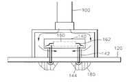
도 1은 종래의 온도 특성 평가용 테스트 보드를 설명하기 위한 수직 단면도이다. 도 1에서 100은 온도 변화 장치(미도시) 즉, 핫/콜(hot/cold) 증기 발생장치에 연결된 튜브를 나타내고, 120은 테스트 보드를 나타내고, 140은 테스트 보드상에 고정된 소켓을 나타내고, 160은 소켓내에 수용된 패키지된 반도체 디바이스를 나타낸다.1 is a vertical cross-sectional view illustrating a conventional test board for evaluation of temperature characteristics. In FIG. 1, 100 represents a tube connected to a temperature change device (not shown), that is, a hot / cold steam generator, 120 represents a test board, 140 represents a socket fixed on the test board, 160 represents a packaged semiconductor device contained within a socket.
여기서, 소켓(140)으로부터 뻗어 있는 소켓 핀(142)의 일측은 테스트 보드(120)를 관통하여 테스트 보드(120)의 하부면상에 납땜되어 있고, 반도체 디바이스(160)의 리드(lead)(162)는 소켓(140)내에 있는 소켓 핀(142)의 타측에 탑재되어 있다.Here, one side of the
도 1에 도시된 바와 같이, 온도 특성 평가시에 반도체 디바이스(160)는 소켓(140)을 통해 테스트 보드(120)에 연결되어 있다. 현재 사용되는 대부분의 온도 변화 장치는 핫/콜 증기를 이용하여 측정하고자하는 디바이스(160)를 측정 온도로 유지시킨다. 온도 특성 검토는 측정 온도에서 보통 5분이상 유지되므로, 테스트 보드(120) 역시 동일한 시간에서 동일한 온도로 유지되어야 한다.As shown in FIG. 1, in the temperature characteristic evaluation, the
그러나, 테스트 보드(120)의 상부와 하부에는 온도차가 생기며, 특히 0℃ 이하의 저온에서는 이러한 온도차로 인해 테스트 보드(120)의 하부면의 납땜 부위(144)에 물방울(180)이 생긴다. 즉, 이 납땜 부위(144)는 테스트 보드(120)의 상부면의 온도가 전도되어 온도차가 가장 극심한 부위이므로, 주위의 온도차에 의해 물방울(180)이 맺히게 된다. 이러한 물방울(180)은 주위의 다른 납땜 부위의 물방울과 합쳐져서 납땝 부위들을 서로 단락시키고, 결국 소켓 핀과 핀 사이에 경로가 형성되어 누설을 발생시킨다. 또한, 심하게는 디바이스 리드(162)와 소켓(140)의 접촉면 사이에 습기가 침투하여 테스트를 불가능하게 만든다.However, a temperature difference occurs between the upper part and the lower part of the
따라서, 이러한 테스트 보드(120)의 조건으로 인해 온도 특성 평가가 정확하게 이루어 질수 없으며, 심지어 테스트를 불가능하게 만든다. 이러한 경우에, 테스트 보드(120)에 묻어 있는 물기를 제거한 후에 다시 테스트를 한다면 시간적인 손실이 매우 크다. 즉, 테스트 보드(120)의 물기를 닦아내고, 건조시키는데 시간이 걸릴뿐만 아니라, 테스트 보드(120)에 연결된 온도 변화 장치(미도시) 및 기타 테스트 장비(미도시)를 다시 세팅하는데도 상당한 시간이 걸리기 때문이다.Therefore, due to the condition of the
본 발명이 이루고자 하는 기술적 과제는, 디바이스의 온도 특성 평가시에 온도 변화에 따라 디바이스에 영향을 미치지 않는 온도 특성 평가용 테스트 보드를 제공하는데 있다.SUMMARY OF THE INVENTION The present invention has been made in an effort to provide a test board for evaluating temperature characteristics that does not affect the device due to temperature change at the time of evaluating temperature characteristics of the device.
상기 과제를 이루기 위하여, 테스트할 반도체 디바이스를 수용하는 소켓을 지지하는 본 발명에 따른 반도체 디바이스의 온도 특성 평가용 테스트 보드는 적어도 하나 이상의 관통 구멍 및 하부 캡을 구비하는 것이 바람직하다. 여기서, 관통 구멍을 소켓의 부근에 배치되어 있으며, 테스트 보드의 상부면과 하부면을 관통한다. 그리고, 하부 캡은 관통 구멍이 위치된 영역 및 테스트 보드의 하부면에 있는 소켓의 납땜 부위들을 소정의 공간을 두고 에워싸고 있다. 이에 따라, 테스트 보드의 상부와 하부를 등온으로 유지함으로써 디바이스의 온도 특성 평가시에 온도 변화에 따라 디바이스에 영향을 미치지 않고 테스트를 원활하게 진행시킨다.In order to achieve the above object, it is preferable that the test board for temperature characteristic evaluation of the semiconductor device according to the present invention supporting the socket for receiving the semiconductor device to be tested has at least one through hole and a lower cap. Here, the through hole is disposed in the vicinity of the socket and penetrates the upper and lower surfaces of the test board. The lower cap surrounds the area where the through hole is located and the soldering portions of the socket on the lower surface of the test board with a predetermined space. Accordingly, by keeping the upper and lower portions of the test board at isothermal temperature, the test proceeds smoothly without affecting the device according to the temperature change during the temperature characteristic evaluation of the device.
이하, 본 발명에 따른 반도체 디바이스의 온도 특성 평가용 테스트 보드의 구성 및 작용을 첨부한 도면을 참조하여 다음과 같이 설명한다.Hereinafter, with reference to the accompanying drawings, the configuration and operation of the test board for evaluation of temperature characteristics of a semiconductor device according to the present invention will be described.
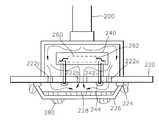
도 2는 본 발명에 따른 온도 특성 평가용 테스트 보드를 설명하기 위한 수직 단면도이다. 도 2에서 200은 온도 변화 장치(미도시) 즉, 핫/콜 증기 발생장치에 연결된 튜브를 나타내고, 220은 테스트 보드를 나타내고, 240은 테스트 보드상에 고정된 소켓을 나타내고, 260은 소켓내에 수용된 패키지된 반도체 디바이스를 나타낸다.2 is a vertical cross-sectional view for explaining a test board for evaluation of temperature characteristics according to the present invention. In FIG. 2, 200 represents a tube connected to a temperature changer (not shown), that is, a hot / call steam generator, 220 represents a test board, 240 represents a socket fixed on the test board, and 260 is housed within the socket. Represents a packaged semiconductor device.
여기서, 소켓(240)으로부터 뻗어 있는 소켓 핀(242)의 일측은 테스트 보드(220)를 관통하여 테스트 보드(220)의 하부면상에 납땜되어 있고, 반도체 디바이스(260)의 리드(262)는 소켓(240)내에 있는 소켓 핀(242)의 타측에 탑재되어 있다.Here, one side of the
도 2에 도시된 본 발명에 따른 테스트 보드(220)는 관통 구멍들(222a 내지 222c) 및 하부 캡(226)을 포함한다.The
관통 구멍들(222a 내지 222b)은 테스트 보드(220)상에 고정된 소켓(240)의 부근 예컨대, 소켓(240)의 바로 밑부분 및 소켓(240)의 측면 부분에 배치되어 있으며, 테스트 보드(220)의 상부면과 하부면을 관통한다.The through
하부 캡(226)은 테스트 보드(220)의 하부에 배치되며, 관통 구멍들(222a 내지 222b)이 위치된 영역 및 테스트 보드(220)의 하부면에 있는 납땜 부위(244)들을 소정의 공간을 두고 에워싸고 있다. 이러한 하부 캡(226)은 테스트 보드(220)의 상부면과 하부면의 온도가 동일하게 유지되도록 하기 위해서 단열재로 되어 있다.The
온도 특성 평가시에, 테스트할 반도체 디바이스(260)는 테스트 보드(220)에 고정된 소켓(240)내에 수용되고, 온도 변화 장치에 연결된 튜브(200)의 끝부분은 도 2에 도시된 바와 같이 소켓(240)을 에워싸도록 배치된다.In evaluating the temperature characteristics, the semiconductor device to be tested 260 is housed in a
튜브(200)로부터 증기가 나오게 되면, 그 증기는 도 2에 화살표로 표시된 바와 같이 튜브(200)의 끝부분으로 에워싸인 테스트 보드(220)의 상부 뿐만 아니라, 하부 캡(226)으로 에워싸인 테스트 보드(220)의 하부로도 관통 구멍들(222a 내지 222c)을 통해 이동한다. 따라서, 튜브(200)의 끝부분 및 하부 캡(226)으로 에워싸인 테스트 보드(220)의 상부와 하부는 어떠한 온도 변화에도 등온을 유지하게 된다.When steam emerges from the
예컨대, 0℃ 이하의 저온에서 온도 특성을 평가하고자 할 경우에도, 테스트 보드(220)의 상부 및 하부는 등온을 유지하게 되므로, 종래와 같이 테스트 보드(220)의 하부면에 있는 납땜 부위(244)에 물방울이 생기지 않는다. 결국, 테스트 보드(220)의 하부를 에워싸는 하부 캡(226)의 내부와 그 외부에는 온도차가 있으므로, 도 2에 도시된 바와 같이 하부 캡(226)의 외부 주위에 물방울(280)이 생기게 된다. 그러나, 하부 캡(226)의 외부 주위에 생긴 물방울(280)은 반도체 디바이스의 온도 특성에 따른 테스시에 아무런 영향을 미치지 않는다.For example, even when a temperature characteristic is to be evaluated at a low temperature of 0 ° C. or lower, the upper and lower portions of the
도 2에 도시된 바에 의하면, 하부 캡(226)은 하나의 실시예로서 테스트 보드(220)에 미리 고정된 캡 물림틀(224)을 통해 테스트 보드(220)에 부착 및 분리가능하게 결합될 수 있다. 예컨대, 임계치 이상의 고온에서 특성 검토가 이루어 질 경우에 하부 캡(226)을 간단하게 분리하여 종래의 테스트 보드처럼 이용할 수도 있다. 임계치 이상의 고온에서는 하부 캡(226) 없이도 납땜 부위(244)에 물방울이 잘 생기지 않기 때문이다. 다른 실시예로서, 하부 캡(226)은 캡 물림틀(224)을 통하지 않고, 테스트 보드(220)에 일체형으로 결합될 수도 있다.As shown in FIG. 2, the
또한, 하부 캡(226)은 테스트 보드(220)의 하부면으로부터 소정 공간을 두고 이격된 밑바닥 부분을 가지며, 그 밑바닥 부분에 제습제(228)를 넣음으로써 하부 캡(226)의 외부 주위에 생긴 물방울(280)로 인하여, 테스트 보드(220)의 하부면과 하부 캡(226)의 밑바닥 부분 사이에 생길 수 있는 습기를 제거한다.In addition, the
지금까지 본 발명에 따른 테스트 보드(220)를 설명하였지만, 전술한 실시예에 제한되지 않고, 그 변형이 가능하다는 것은 본 기술의 당업자에게 명백할 것이다. 예컨대, 관통 구멍의 갯수, 크기 및 그 위치는 임의대로 변형할 수 있으며, 하부 캡의 형상은 도 2에서 각이 지고 볼록한 형상으로 되어 있지만, 테스트 보드(220)의 하부면을 소정 공간을 두고 에워싸는 형상이면 어떤 형상으로도 가능하다.Although the
이상에서 설명한 바와 같이, 본 발명에 의한 온도 특성 평가용 테스트 보드는 테스트 보드의 상부와 하부를 등온으로 유지함으로써 디바이스의 온도 특성 평가시에 디바이스에 영향을 미치지 않고 테스트를 원활하게 진행시키는 이점이 있다.As described above, the test board for temperature characteristic evaluation according to the present invention has the advantage of smoothly proceeding the test without affecting the device during the temperature characteristic evaluation of the device by keeping the upper and lower parts of the test board at isothermal temperature. .
도 1은 종래의 온도 특성 평가용 테스트 보드를 설명하기 위한 수직 단면도이다.1 is a vertical cross-sectional view illustrating a conventional test board for evaluation of temperature characteristics.
도 2는 본 발명에 따른 온도 특성 평가용 테스트 보드를 설명하기 위한 수직 단면도이다.2 is a vertical cross-sectional view for explaining a test board for evaluation of temperature characteristics according to the present invention.
Claims (2)
Translated fromKoreanPriority Applications (1)
| Application Number | Priority Date | Filing Date | Title |
|---|---|---|---|
| KR1019970024915AKR100486194B1 (en) | 1997-06-16 | 1997-06-16 | Test board for temperature characteristic evalution in semiconductor device |
Applications Claiming Priority (1)
| Application Number | Priority Date | Filing Date | Title |
|---|---|---|---|
| KR1019970024915AKR100486194B1 (en) | 1997-06-16 | 1997-06-16 | Test board for temperature characteristic evalution in semiconductor device |
Publications (2)
| Publication Number | Publication Date |
|---|---|
| KR19990001544A KR19990001544A (en) | 1999-01-15 |
| KR100486194B1true KR100486194B1 (en) | 2005-06-16 |
Family
ID=37303033
Family Applications (1)
| Application Number | Title | Priority Date | Filing Date |
|---|---|---|---|
| KR1019970024915AExpired - Fee RelatedKR100486194B1 (en) | 1997-06-16 | 1997-06-16 | Test board for temperature characteristic evalution in semiconductor device |
Country Status (1)
| Country | Link |
|---|---|
| KR (1) | KR100486194B1 (en) |
Families Citing this family (1)
| Publication number | Priority date | Publication date | Assignee | Title |
|---|---|---|---|---|
| JP2002111157A (en)* | 2000-09-27 | 2002-04-12 | Ando Electric Co Ltd | Printed circuit board and its manufacturing method |
Citations (4)
| Publication number | Priority date | Publication date | Assignee | Title |
|---|---|---|---|---|
| JPS60128629A (en)* | 1983-12-16 | 1985-07-09 | Toshiba Corp | Method of measurement of semiconductor element |
| JPH06118136A (en)* | 1992-10-07 | 1994-04-28 | Mitsubishi Electric Corp | Low temperature handler |
| JPH07209373A (en)* | 1993-11-30 | 1995-08-11 | Nec Corp | Cooling tester |
| US5977785A (en)* | 1996-05-28 | 1999-11-02 | Burward-Hoy; Trevor | Method and apparatus for rapidly varying the operating temperature of a semiconductor device in a testing environment |
- 1997
- 1997-06-16KRKR1019970024915Apatent/KR100486194B1/ennot_activeExpired - Fee Related
Patent Citations (4)
| Publication number | Priority date | Publication date | Assignee | Title |
|---|---|---|---|---|
| JPS60128629A (en)* | 1983-12-16 | 1985-07-09 | Toshiba Corp | Method of measurement of semiconductor element |
| JPH06118136A (en)* | 1992-10-07 | 1994-04-28 | Mitsubishi Electric Corp | Low temperature handler |
| JPH07209373A (en)* | 1993-11-30 | 1995-08-11 | Nec Corp | Cooling tester |
| US5977785A (en)* | 1996-05-28 | 1999-11-02 | Burward-Hoy; Trevor | Method and apparatus for rapidly varying the operating temperature of a semiconductor device in a testing environment |
Also Published As
| Publication number | Publication date |
|---|---|
| KR19990001544A (en) | 1999-01-15 |
Similar Documents
| Publication | Publication Date | Title |
|---|---|---|
| US6573743B2 (en) | Testing apparatus for test piece, testing method, contactor and method of manufacturing the same | |
| US7138811B1 (en) | Seals used for testing on an integrated circuit tester | |
| KR100471357B1 (en) | Carrier Module for Semiconductor Test Handler | |
| KR970062714A (en) | Contact inspection device for checking the contact failure of the processor and integrated circuit device inspection system incorporating the same | |
| US8106671B2 (en) | Socketless integrated circuit contact connector | |
| KR100486194B1 (en) | Test board for temperature characteristic evalution in semiconductor device | |
| US9476936B1 (en) | Thermal management for microcircuit testing system | |
| KR100422341B1 (en) | package test socket | |
| KR200312425Y1 (en) | Contactor for Testing Microwave Device | |
| KR20030068629A (en) | Test board assemble | |
| KR100844486B1 (en) | Semiconductor chip test socket | |
| JP2000150598A (en) | Contactor and its manufacture | |
| KR100391822B1 (en) | Test fixture for semiconductor package using computer mother board | |
| KR950009876Y1 (en) | Test board device of semiconductor test equipment | |
| KR100729052B1 (en) | Universal socket for semiconductor package test | |
| KR0154731B1 (en) | Inspecting apparatus with power control circuit | |
| KR100331262B1 (en) | Connection state test circuit of BGA package | |
| KR20080053120A (en) | Universal Package Test Board Assembly | |
| KR980012339A (en) | Semiconductor package test board | |
| KR200171210Y1 (en) | Multi thermal cap of thermostream | |
| KR20000012577U (en) | Test device for semiconductor package | |
| KR100253278B1 (en) | Integrated circuit test socket | |
| KR200165882Y1 (en) | Semiconductor Package Test Device | |
| KR100290440B1 (en) | Variable element mounting structure of the probe card | |
| JPS5838876A (en) | Testing of semiconductor device |
Legal Events
| Date | Code | Title | Description |
|---|---|---|---|
| PA0109 | Patent application | St.27 status event code:A-0-1-A10-A12-nap-PA0109 | |
| R17-X000 | Change to representative recorded | St.27 status event code:A-3-3-R10-R17-oth-X000 | |
| R18-X000 | Changes to party contact information recorded | St.27 status event code:A-3-3-R10-R18-oth-X000 | |
| PG1501 | Laying open of application | St.27 status event code:A-1-1-Q10-Q12-nap-PG1501 | |
| PN2301 | Change of applicant | St.27 status event code:A-3-3-R10-R13-asn-PN2301 St.27 status event code:A-3-3-R10-R11-asn-PN2301 | |
| PN2301 | Change of applicant | St.27 status event code:A-3-3-R10-R13-asn-PN2301 St.27 status event code:A-3-3-R10-R11-asn-PN2301 | |
| R18-X000 | Changes to party contact information recorded | St.27 status event code:A-3-3-R10-R18-oth-X000 | |
| PN2301 | Change of applicant | St.27 status event code:A-3-3-R10-R13-asn-PN2301 St.27 status event code:A-3-3-R10-R11-asn-PN2301 | |
| A201 | Request for examination | ||
| PA0201 | Request for examination | St.27 status event code:A-1-2-D10-D11-exm-PA0201 | |
| R18-X000 | Changes to party contact information recorded | St.27 status event code:A-3-3-R10-R18-oth-X000 | |
| R18-X000 | Changes to party contact information recorded | St.27 status event code:A-3-3-R10-R18-oth-X000 | |
| R18-X000 | Changes to party contact information recorded | St.27 status event code:A-3-3-R10-R18-oth-X000 | |
| R17-X000 | Change to representative recorded | St.27 status event code:A-3-3-R10-R17-oth-X000 | |
| D13-X000 | Search requested | St.27 status event code:A-1-2-D10-D13-srh-X000 | |
| D14-X000 | Search report completed | St.27 status event code:A-1-2-D10-D14-srh-X000 | |
| E902 | Notification of reason for refusal | ||
| PE0902 | Notice of grounds for rejection | St.27 status event code:A-1-2-D10-D21-exm-PE0902 | |
| E601 | Decision to refuse application | ||
| PE0601 | Decision on rejection of patent | St.27 status event code:N-2-6-B10-B15-exm-PE0601 | |
| J201 | Request for trial against refusal decision | ||
| PJ0201 | Trial against decision of rejection | St.27 status event code:A-3-3-V10-V11-apl-PJ0201 | |
| AMND | Amendment | ||
| P11-X000 | Amendment of application requested | St.27 status event code:A-2-2-P10-P11-nap-X000 | |
| P13-X000 | Application amended | St.27 status event code:A-2-2-P10-P13-nap-X000 | |
| PB0901 | Examination by re-examination before a trial | St.27 status event code:A-6-3-E10-E12-rex-PB0901 | |
| B701 | Decision to grant | ||
| PB0701 | Decision of registration after re-examination before a trial | St.27 status event code:A-3-4-F10-F13-rex-PB0701 | |
| GRNT | Written decision to grant | ||
| PR0701 | Registration of establishment | St.27 status event code:A-2-4-F10-F11-exm-PR0701 | |
| PR1002 | Payment of registration fee | St.27 status event code:A-2-2-U10-U11-oth-PR1002 Fee payment year number:1 | |
| PG1601 | Publication of registration | St.27 status event code:A-4-4-Q10-Q13-nap-PG1601 | |
| PN2301 | Change of applicant | St.27 status event code:A-5-5-R10-R13-asn-PN2301 St.27 status event code:A-5-5-R10-R11-asn-PN2301 | |
| PN2301 | Change of applicant | St.27 status event code:A-5-5-R10-R13-asn-PN2301 St.27 status event code:A-5-5-R10-R11-asn-PN2301 | |
| LAPS | Lapse due to unpaid annual fee | ||
| PC1903 | Unpaid annual fee | St.27 status event code:A-4-4-U10-U13-oth-PC1903 Not in force date:20080422 Payment event data comment text:Termination Category : DEFAULT_OF_REGISTRATION_FEE | |
| PC1903 | Unpaid annual fee | St.27 status event code:N-4-6-H10-H13-oth-PC1903 Ip right cessation event data comment text:Termination Category : DEFAULT_OF_REGISTRATION_FEE Not in force date:20080422 | |
| R18-X000 | Changes to party contact information recorded | St.27 status event code:A-5-5-R10-R18-oth-X000 | |
| P22-X000 | Classification modified | St.27 status event code:A-4-4-P10-P22-nap-X000 |