KR100483636B1 - Method and apparatus for design verification using emulation and simulation - Google Patents
Method and apparatus for design verification using emulation and simulationDownload PDFInfo
- Publication number
- KR100483636B1 KR100483636B1KR1019970053374AKR19970053374AKR100483636B1KR 100483636 B1KR100483636 B1KR 100483636B1KR 1019970053374 AKR1019970053374 AKR 1019970053374AKR 19970053374 AKR19970053374 AKR 19970053374AKR 100483636 B1KR100483636 B1KR 100483636B1
- Authority
- KR
- South Korea
- Prior art keywords
- event
- design
- simulation
- microprocessor
- reconfigurable
- Prior art date
- Legal status (The legal status is an assumption and is not a legal conclusion. Google has not performed a legal analysis and makes no representation as to the accuracy of the status listed.)
- Expired - Fee Related
Links
Images


Classifications
- G—PHYSICS
- G06—COMPUTING OR CALCULATING; COUNTING
- G06F—ELECTRIC DIGITAL DATA PROCESSING
- G06F8/00—Arrangements for software engineering
- G—PHYSICS
- G06—COMPUTING OR CALCULATING; COUNTING
- G06F—ELECTRIC DIGITAL DATA PROCESSING
- G06F30/00—Computer-aided design [CAD]
- G06F30/30—Circuit design
- G06F30/32—Circuit design at the digital level
- G06F30/33—Design verification, e.g. functional simulation or model checking
- G06F30/3308—Design verification, e.g. functional simulation or model checking using simulation
- G06F30/331—Design verification, e.g. functional simulation or model checking using simulation with hardware acceleration, e.g. by using field programmable gate array [FPGA] or emulation
Landscapes
- Engineering & Computer Science (AREA)
- Computer Hardware Design (AREA)
- Theoretical Computer Science (AREA)
- Physics & Mathematics (AREA)
- General Engineering & Computer Science (AREA)
- General Physics & Mathematics (AREA)
- Evolutionary Computation (AREA)
- Geometry (AREA)
- Software Systems (AREA)
- Design And Manufacture Of Integrated Circuits (AREA)
- Test And Diagnosis Of Digital Computers (AREA)
- Tests Of Electronic Circuits (AREA)
- Management, Administration, Business Operations System, And Electronic Commerce (AREA)
Abstract
Translated fromKoreanDescription
Translated fromKorean본 발명은 논리 설계를 검증하기 위해 에뮬레이션과 시뮬레이션을 결합시키는 것에 관한 것이다.The present invention relates to combining emulation and simulation to verify a logic design.
에뮬레이션 제조 전에 시스템 및 집적회로는 기능적으로 테스트하기 위한 회로 및 시스템 설계자의 강력한 방법을 제공한다. 회로 설계자 및 엔지니어는 설계를 일시 동작 하드웨어(temporary operating hardware)로 전환하기 위해 에뮬레이터를 이용하여, 엔지니어가 실시간 조건에서 또는 그 조건에 근접하여 설계를 테스트할 수 있게 한다. 부가적으로, 엔지니어는 집적 회로, 시스템 하드웨어, 및 소프트웨어를 동시에 검증할 수 있다. 에뮬레이션 시스템의 예가 샘플 등의 미국 특허 제5,109,353호 및 버츠 등의 미국 특허 제5,036,473호에 설명되어 있으며, 상기 양 특허는 본 명세서에 참조로서 고려된다.Prior to emulation manufacture, systems and integrated circuits provide a powerful way for circuit and system designers to functionally test. Circuit designers and engineers use emulators to turn designs into temporary operating hardware, enabling engineers to test the design at or near real-time conditions. In addition, engineers can simultaneously verify integrated circuits, system hardware, and software. Examples of emulation systems are described in US Pat. No. 5,109,353 to Sample et al. And US Pat. No. 5,036,473 to Burtz et al., Both of which are incorporated herein by reference.
전형적으로, 설계 프로세스는 초기 설계 아이디어 레벨에서 상세한 제조 레벨까지의 설계의 다수의 변형들(transformation)을 포함한다. 엔지니어는 설계 아이디어로부터 시작할 것이다. 이어서 엔지니어는 설계 아이디어의 행위 정의(behavioral definition)를 발생시킬 것이다. 행위 설계(behavioral design)의 결과는 플로우챠트이거나 또는 플로우 그래프일 것이다. 다음으로, 엔지니어는 시스템 데이터 경로를 설계할 수 있으며 시스템의 구현에 필요한 레지스터 및 논리 유닛을 명기할 수 있다. 이 단계에서, 엔지니어는 버스를 통한 레지스터와 논리 유닛간의 데이터의 이동을 제어하는 절차를 성립시킬 수 있다. 설계 프로세스에서 논리 설계가 다음 단계로서, 이에 의해 엔지니어는 데이터 레지스터, 버스, 논리 유닛, 및 그것의 제어 하드웨어의 구현을 위해 프리머티브 게이트들(primitive gate) 및 플립-플롭을 이용한다. 이 설계 단계의 결과는 게이트 및 플립-플롭의 넷리스트(netlist)이다.Typically, the design process includes a number of transformations of the design from the initial design idea level to the detailed manufacturing level. The engineer will start with the design idea. The engineer will then generate a behavioral definition of the design idea. The result of a behavioral design may be a flowchart or a flow graph. Next, engineers can design the system data path and specify the registers and logic units needed to implement the system. At this stage, engineers can establish procedures to control the movement of data between registers and logic units across the bus. Logic design is the next step in the design process, whereby the engineer uses primitive gates and flip-flops for the implementation of data registers, buses, logic units, and its control hardware. The result of this design step is a netlist of gates and flip-flops.
다음 설계 단계는 게이트 및 플립-플롭의 넷리스트를 트랜지스터 리스트(transistor list) 또는 레이아웃으로 변환한다. 따라서, 게이트 및 플립-플롭은 그것의 트랜지스터 등가물 또는 라이브러리 셀들로 교체된다. 셀 및 트랜지스터 선택 프로세스 동안에, 타이밍 및 로딩 요구가 고려된다. 최종적으로, 설계가 제조되며, 이에 의해 프로그램가능한 디바이스의 퓨즈를 가열하거나(burn) 집적회로 제조를 위한 마스크를 발생하기 위해 트랜지스터 리스트 또는 레이아웃 명세가 사용된다.The next design step converts the netlist of gates and flip-flops into a transistor list or layout. Thus, the gate and flip-flop are replaced with its transistor equivalent or library cells. During the cell and transistor selection process, timing and loading requirements are considered. Finally, the design is manufactured, whereby a transistor list or layout specification is used to burn the fuse of the programmable device or generate a mask for integrated circuit fabrication.
하드웨어 기술 언어들("HLD")은 상술된 다양한 설계 단계의 출력을 표현하는 다양한 포맷을 제공한다. 이 언어는 기능 블록의 게이트 레벨 기술 및 완전 시스템들(complete system)의 하이 레벨 기술(High-level description)을 포함하는 다양한 레벨에서 회로를 생성하기 위해 사용될 수 있다. 따라서, HDL은 추상화된 많은 레벨에서 전자 시스템을 기술할 수 있다.Hardware description languages (“HLD”) provide a variety of formats for representing the output of the various design steps described above. This language can be used to create circuits at various levels, including gate level descriptions of functional blocks and high-level descriptions of complete systems. Thus, HDL can describe electronic systems at many levels of abstraction.
하드웨어 기술 언어는 설계의 시뮬레이션, 모델링, 테스팅, 생성 및 문서화(documentation)를 목적으로 하드웨어를 기술하기 위해 사용된다. 이전에, 회로 설계자는 논리 게이트 레벨에서 설계하려는 경향이 있었다. 점차로, 설계자는 특히, HDL 방법론을 이용하여 더욱 하이 레벨로 설계하고 있다. HDL은 설계의 기능 및 배선 세부사항의 표현을 위한 편리한 포맷을 제공하며 추상화된 1개 이상의 레벨로 하드웨어를 표현할 수 있다.Hardware description language is used to describe hardware for the purpose of simulation, modeling, testing, generation, and documentation of a design. Previously, circuit designers tended to design at the logic gate level. Increasingly, designers are designing at higher levels, especially using the HDL methodology. HDL provides a convenient format for representing design features and wiring details, and can represent hardware at one or more levels of abstraction.
2개의 인기있는 하드웨어 기술 언어가 베리로그(Verilog) 및 초고속 집적회로(Very-High-Speed Integrated Circuit; VHSIC) 하드웨어 기술 언어("VHDL")이다. VHDL은 1980년대 초기에 미국 국방성에서 시작하였으며 처음에는 디지털 하드웨어 시스템을 기술하기 위한 문서화 언어로서 시작되었다. 이후에, 이 언어는 기술(description)이 시뮬레이션되고 합성될 수 있도록 세련되었다. 설계 엔트리(design entry), 시뮬레이션 및 합성을 포함하는 HDL-기본 설계 툴의 등장은 결과적으로 VHDL의 초점을 설계 문서화로부터 하이 레벨 설계로 이양시켰다. 다른 하드웨어 기술 언어는 다음과 같은 것을 포함하며, 그에 한정되는 것은 아니다; 하드웨어 프로그래밍 언어(A Hardware Programming Language; AHPL), 컴퓨터 설계 언어(Computer Design Language; CDL), 컨센서스 랭귀지(CONsensus LANguage; CONLAN), 대화형 설계 언어(Interactive Design Language; IDL), 명령어 집합 프로세서 규약(Instruction Set Processor Specification; ISPS), 테스트 발생 및 시뮬레이션(Test Generation And Simulation; TEGAS), 텍사스 인스트루먼츠 하드웨어 기술 언어(Texas Instrument Hardware Description Language; Ti-HDL), 도시바 기술 언어(Toshiba Description Language; TDL), ZEUS, 및 NDL.Two popular hardware description languages are Verilog and Very-High-Speed Integrated Circuit (VHSIC) hardware description language ("VHDL"). VHDL started with the US Department of Defense in the early 1980s and initially as a documentation language for describing digital hardware systems. Later, the language was refined so that descriptions could be simulated and synthesized. The emergence of HDL-based design tools, including design entry, simulation, and synthesis, has in turn shifted the focus of VHDL from design documentation to high-level designs. Other hardware description languages include, but are not limited to: A Hardware Programming Language (AHPL), Computer Design Language (CDL), Consensus LANguage (CONLAN), Interactive Design Language (IDL), Instruction Set Processor Conventions Set Processor Specification (ISPS), Test Generation And Simulation (TEGAS), Texas Instrument Hardware Description Language (Ti-HDL), Toshiba Description Language (TDL), ZEUS, And NDL.
시뮬레이션은 오랫동안 복잡한 전자 회로 설계의 논리적 교정의 검증을 위한 양호한 방법이었다. 시뮬레이션은 임의의 자극이 가해지는 경우, 제조되고 테스트된 설계와 유사한 방식으로 응답하는 모델의 생성으로서 광범위하게 정의되었다. 보다 구체적으로, "시뮬레이션"이라는 용어는 전형적으로 그러한 모델이 컴퓨터 프로그램으로서 수행되는 경우에 사용된다. 그와 대조적으로, "에뮬레이션"은 프로그램가능(혹은 재구성가능) 논리 또는 필드-프로그래머블 게이트 어레이(FPGA) 디바이스를 이용하는 모델의 생성이다. 시뮬레이션은 설계자의 비싼 제조 프로세스가 수행되기 이전에 설계상의 에러를 검출할 수 있게 하기 때문에 많은 양의 시간 및 재정 자원을 절감한다. 더욱이, 설계 프로세스 그 자체는 새로운 제품의 초기 일반적인 개념이 상세한 청사진으로 변환되는 일련의 단계들로서 보여질 수 있다. 이러한 프로세스의 초기 단계에서의 에러의 검출은 또한 시간 및 엔지니어링 자원을 절감한다.Simulation has long been a good method for verifying the logical calibration of complex electronic circuit designs. Simulation is broadly defined as the generation of a model that responds in a similar fashion to the manufactured and tested design when any stimulus is applied. More specifically, the term "simulation" is typically used when such a model is performed as a computer program. In contrast, “emulation” is the creation of a model using a programmable (or reconfigurable) logic or field-programmable gate array (FPGA) device. Simulation saves a lot of time and financial resources because it allows designers to detect design errors before expensive manufacturing processes are performed. Moreover, the design process itself can be seen as a series of steps where the initial general concept of a new product is translated into a detailed blueprint. Detection of errors at an early stage of this process also saves time and engineering resources.
시뮬레이터는 2가지 종류로 분류될 수 있다. 제1 종류의 시뮬레이터는 레벨화된 시뮬레이션 원리(levelized simulation principle)를 따르며, 제2 종류는 이벤트-중심 시뮬레이션 원리(event-driven simulation principle)를 따른다. 각 시뮬레이션 사이클에서, 레벨화된 시뮬레이터는 컴포넌트의 입력 신호가 변화되는 것에 상관없이 시뮬레이션된 설계의 모든 컴포넌트의 새로운 상태를 재평가해야 한다. 부가적으로 상태가 변화되지 않았을지라도 컴포넌트의 상태는 재전송되어야 한다. 이벤트 중심 시뮬레이터는 어떤 입력 조건이 현재의 시뮬레이션 사이클에서 변화하는 컴포넌트만을 평가한다. 결과적으로, 이벤트 중심 시뮬레이터는 컴포넌트 평가 시간의 현저한 절감을 실현한다. 그러나, 현저한 부가적 소프트웨어 실행 시간이 특정 컴포넌트가 평가되어야 하는 지에 대한 결정 수립에 소비된다. 그 결과, 두가지 종류의 종래의 시뮬레이터(레벨화된 시뮬레이터 및 이벤트 중심 시뮬레이터)는 유사한 성능을 갖는다.Simulators can be classified into two types. The first kind of simulator follows the leveled simulation principle, and the second kind follows the event-driven simulation principle. In each simulation cycle, the leveled simulator must re-evaluate the new state of all components of the simulated design, regardless of which component's input signal changes. Additionally, the state of the component must be retransmitted even if the state has not changed. Event-driven simulators only evaluate components whose input conditions change in the current simulation cycle. As a result, the event driven simulator realizes significant savings in component evaluation time. However, significant additional software execution time is spent making decisions about whether a particular component should be evaluated. As a result, both kinds of conventional simulators (leveled simulators and event driven simulators) have similar performance.
시뮬레이션에 대한 에뮬레이션의 제1 장점은 속도이다. 에뮬레이션은 검증 하에 있는 각 컴포넌트를 물리적으로 상이한 프로그램가능한 논리 디바이스로 맵핑하여 그러한 모든 컴포넌트가 동시에 검증된다. 그러나, 전형적인 시뮬레이터에서, 단일 프로세싱 엘리먼트는 각 시뮬레이션 시간 단계에서 각 컴포넌트의 다음 상태를 연속적으로 계산한다.The first advantage of emulation over simulation is speed. Emulation maps each component under verification to a physically different programmable logic device so that all such components are verified at the same time. However, in a typical simulator, a single processing element continuously calculates the next state of each component at each simulation time step.
에뮬레이션은 논리 게이트의 네트워크로서 표현되거나 또는 네트워크로 용이하게 변환된 설계에 대한 효율적인 검증 기술(verification technology)이다. 그러나, 현대의 설계 방법론은 초기 설계 단계에서, 큰 설계부가 행위 모델(behavioral model)로서 표현될 것을 필요로 한다. 일련의 설계 결정을 통해서 이와 같은 행위 모델은 점차로 동등한 구조 기술로 교체된다. 각 교체 단계의 교정은 어떤 지점에서 설계 그 자체가 행위적, 구조적, 및 게이트 레벨 컴포넌트의 복잡화된 혼합으로서 표현되는 지가 검증된다. 설계의 구조적 부분은 광범위하게 유용한 논리 합성 프로그램을 이용하여 에뮬레이션 하드웨어 내로 직접적으로 맵핑된다. 그러나, 행위 부분(behavioral portion)은 컴퓨터 프로그램으로 컴파일되고 실행되기만 할 수 있다. 그 성질에 의해, 에뮬레이션은 실제 하드웨어를 이용하여 모델을 생성할 것을 필요로 하며 따라서 새로운 제품의 개념이 그 기능의 하이 레벨 기술에 의하지 않고서는 그 컴포넌트에 의해 표현되지 않는 경우에 설계 사이클의 초기 단계에서 사용될 수 없다. 따라서, 설계 단계의 초기에 검증을 수행하기 위해, 가장 적합한 환경은 에뮬레이션 및 행위 시뮬레이션의 특성을 효율적으로 결합시킬 것이다. 또한, 에뮬레이션과 시뮬레이션을 결합시킴으로써 설계자가 아날로그 신호와 같은 물리적 제약조건 때문에 에뮬레이션될 수 없는 설계 컴포넌트를 시뮬레이션할 수 있게 한다.Emulation is an efficient verification technology for a design that is represented as a network of logic gates or easily converted to a network. However, modern design methodologies require that, at an early design stage, a large design part be represented as a behavioral model. Through a series of design decisions, these behavior models are gradually replaced by equivalent structural techniques. The calibration of each replacement step verifies at what point the design itself is represented as a complex mixture of behavioral, structural, and gate level components. The structural part of the design is directly mapped into the emulation hardware using a wide variety of logical synthesis programs. However, the behavioral portion may only be compiled and executed as a computer program. By its nature, emulation requires the creation of a model using real hardware, so that the initial stage of the design cycle is when a new product concept is not represented by that component without high-level description of the function. Cannot be used in Thus, to perform verification early in the design phase, the most appropriate environment will efficiently combine the characteristics of emulation and behavior simulation. In addition, combining emulation and simulation allows designers to simulate design components that cannot be emulated because of physical constraints such as analog signals.
설계가 완료되어 감에 따라, 행위 시뮬레이션에서 논리 에뮬레이션으로 주안점이 이양된다. 그러나, 미래의 제품의 동작 환경을 나타내는 부분은 결코 구조 기술로 변환될 수 없다. 이러한 경우에, 시스템 레벨 환경의 행위 기술(behavioral description)은 에뮬레이션된 설계를 위한 테스트 벤치로서의 역할을 한다. 시스템 레벨 기술(system-level description)은 테스트 자극(test stimulus)을 생성하고 실제 동작 조건을 아주 유사하게 복사하는 방법으로 검증 하에 있는 설계의 응답을 평가한다. 그러한 행위 테스트 벤치를 실행할 필요성은 하나의 논리 검증 시스템에서 시뮬레이션 및 에뮬레이션 기능을 결합하는 다른 동기이다.As the design completes, the focus shifts from behavior simulation to logic emulation. However, the part that represents the operating environment of future products can never be converted to structural technology. In this case, the behavioral description of the system level environment serves as a test bench for the emulated design. System-level descriptions evaluate the response of a design under validation by generating test stimulus and copying the actual operating conditions very similarly. The need to run such behavior test benches is another motivation to combine simulation and emulation functions in one logical verification system.
에뮬레이션과 시뮬레이션을 결합시키는 한 방법은 신호 상태의 이벤트 또는 변화를 네트워크 인터페이스 상의 설계의 에뮬레이션된 부분으로 또는 에뮬레이션된 부분으로부터 통신하는 호스트 워크스테이션 (또는 그 네트워크) 상에서 시뮬레이터를 실행시키는 것이다. 그러나, 그러한 방법에서, 이벤트 전달의 속도는 성능을 크게 제한한다. 실험에 의하면, SUN 워크스테이션 컴퓨터(예, SPARC-20) 상에서 실행되는 전송 제어 프로토콜(TCP) 상에서 4-바이트 데이터 패킷을 전달하는 평균 시간은 50 마이크로초 내외이다. 그와 같은 크기의 데이터 패킷이 이벤트 및 시뮬레이션 사이클 당 1000 이벤트의 주어진 평균 설계 활동성을 인코딩하기 위해 사용된다고 가정하면, 시뮬레이션의 속도는 초당 20 사이클로 한정될 것이다. 따라서, 현재 게이트 레벨 기술, 구조 기술 및 행위 기술의 혼합일 수 있는 회로 설계를 효율적으로 검증하기 위해 에뮬레이션과 시뮬레이션을 결합시킬 필요성이 존재한다.One way to combine emulation and simulation is to run a simulator on a host workstation (or its network) that communicates events or changes in signal status to or from an emulated portion of the design on a network interface. However, in such a method, the rate of event delivery greatly limits performance. Experiments have shown that the average time to deliver a 4-byte data packet on Transmission Control Protocol (TCP) running on a SUN workstation computer (eg SPARC-20) is around 50 microseconds. Assuming that such data packets are used to encode a given average design activity of 1000 events per event and simulation cycle, the speed of the simulation will be limited to 20 cycles per second. Thus, there is a need to combine emulation and simulation to efficiently validate circuit designs that can be a mix of current gate level technology, structural technology, and behavioral technology.
따라서, 본 발명의 일반적인 목적은 논리 설계의 시뮬레이션과 에뮬레이션을 효율적으로 결합시키는 장치 및 방법을 제공하여, 시뮬레이션된 그리고 에뮬레이션된 설계 부분간의 이벤트 전송의 오버헤드가 최소화되게 하는 것이다.It is therefore a general object of the present invention to provide an apparatus and method for efficiently combining simulation and emulation of a logic design so that the overhead of event transmission between simulated and emulated design parts is minimized.
상기 목적을 실현하기 위해, 상기 설계 검증 방법 및 장치는 검증 하에 있는 논리 설계의 일부분을 에뮬레이션하는데 사용되는 적어도 하나의 재구성가능한 디바이스를 포함한다. 부가적으로, 행위 기술로서 표현될 수 있는 다른 설계 부분을 시뮬레이션하기 위해 적어도 하나의 마이크로프로세서가 사용된다. 이 마이크로프로세서는 시뮬레이션된 부분과 에뮬레이션된 부분 간의 데이터 전송 시간을 최소화하는 방법으로 재구성가능한 디바이스에 접속된다. 또한, 설계의 검증 동안에 이벤트를 검출하기 위해 이벤트 검출기가 제공된다. 마이크로프로세서는 그러한 이벤트 검출 기능을 수행하는 것으로부터 해방되고, 이에 의해 설계 검증 시간을 절감한다.To achieve the above object, the design verification method and apparatus includes at least one reconfigurable device used to emulate a portion of the logical design under verification. Additionally, at least one microprocessor is used to simulate other parts of the design that can be represented as behavioral techniques. The microprocessor is connected to a reconfigurable device in a way that minimizes data transfer time between the simulated and emulated portions. In addition, an event detector is provided to detect the event during verification of the design. The microprocessor is freed from performing such event detection functions, thereby saving design verification time.
본 발명의 다른 목적, 장점, 및 특성이 당분야의 숙련된 사람에게 있어 다음의 명세서 및 도면을 연구함으로써 더욱 명확해질 것이다.Other objects, advantages, and features of the present invention will become more apparent to those skilled in the art from studying the following specification and drawings.
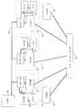
도 1은 논리 검증 시스템의 양호한 실시예의 도면이다. 이 시스템은 프로그램가능한 상호접속부(12)를 사용하여 상호접속된 프로그램가능한 게이트 어레이("FPGA") 디바이스(10)일 수 있는 하나 이상의 재구성가능한 논리 컴포넌트를 포함한다. 상호접속부(12)는 그에 접속된 디바이스의 몇 개의 입력 또는 출력간의 임의의 접속을 생성하도록 프로그램될 수 있다. 장치는 또한 하나 이상의 시뮬레이션 모듈(14)을 포함한다(예시의 목적상 3개가 도시되어 있음). 각각의 시뮬레이션 모듈(14)은 마이크로프로세서 버스(18)를 통해 하나 이상의 임의 접근 메모리 디바이스(20), FPGA(22)일 수 있는 하나 이상의 재구성가능한 논리 컴포넌트, 및 시스템 버스 제어기(24)로 접속된 마이크로프로세서(16)를 포함한다. 비록 도 1에는 하나의 임의 접근 메모리 디바이스(20), 및 하나의 FPGA(22) 만이 도시되어 있으나, 당분야의 숙련공이라면 몇 개의 메모리 디바이스(20) 또는 FPGA(22)가 채용될 수 있다는 것이 알 수 있을 것이다. 또한, 어떤 종류의 메모리도 임의 접근 메모리(20)의 기능을 유사하게 수행하는데 사용될 수 있다. 부가적으로, PAL 또는 PLA같은 다른 종류의 재구성가능한 논리 컴포넌트가 FPGA(10, 22)의 기능을 수행할 수 있다. 어떤 종류의 FPGA를 사용할 것인가는 순전히 설계자의 선택의 문제이다. 양호한 실시예에서, Xilinx, Inc(사)로부터의 4036EX 디바이스가 사용되었다. 이 디바이스는 본 명세서에 참조로서 고려되는 Xilinx 사의 1996년 6월호 PN 0010303, 프로그램가능한 논리 데이터 북(Programmable Logic Data Book)에 설명되어 있다. 어떤 CPU(16)를 사용할 것인가도 또한 설계자의 선택의 문제이다. 양호한 실시예에서, IBM(사)로부터의 PPC403GC CPU 칩이 사용되었다. 각 시뮬레이션 모듈(14) 내의 각 FPGA 디바이스들(22)은 또한 프로그램가능한 상호접속부(12)에 접속된다.1 is a diagram of a preferred embodiment of a logic verification system. The system includes one or more reconfigurable logic components that may be programmable gate array (“FPGA”)
FPGA 디바이스(10)는 버츠 등의 미국 특허 제5,036,473호에 개시된 바와 같이, 컴포넌트의 상호접속으로서 나타나는 검증 하에 있는 논리 회로 부분을 에뮬레이션한다. 시뮬레이션 모듈(14)은 행위 기술에 의해 표현될 수 있는 검증 하에 있는 논리 회로 부분을 시뮬레이션한다. 모듈(14) 내에는, 마이크로프로세서(16)가 행위 기술의 프래그먼트를 선택적으로 실행한다. FPGA(22) 내에서 구현되는 하드웨어 논리는 실행될 행위 프래그먼트 및 실행의 순서를 선택한다. 종래 기술에서 공지된 이벤트-중심 시뮬레이터와는 달리, 마이크로프로세서(16)는 검출, 스케줄, 및 이벤트의 순서 정렬(ordering the event)의 기능으로부터 해방된다. 그 결과, 시뮬레이션 속도가 극적으로 향상된다. FPGA 디바이스(22)는 또한 컴포넌트의 상호접속에 의해 표현되는 행위 기술부분와 그것의 설계부분 사이에 공유된 신호값을 통신한다. 부가적으로, FPGA(22)은 상이한 시뮬레이션 모듈(14) 간에 공유된 신호값을 통신한다.
FPGA 디바이스(22)가 컴포넌트 상호접속으로서 표현된 논리 회로 부분을 에뮬레이션하지 않는다는 것은 본 발명에 있어서 필수인 것은 아니다. 유사하게, FPGA 디바이스(10)가 마이크로프로세서(16)에 의한 실행을 위한 행위 코드 프래그먼트의 선택 및 순서를 결정하는 논리를 수행하지 않는다는 것이 본 발명에 필수인 것은 아니다. 오히려, 양호한 실시예에서, 본 발명은 FPGA 디바이스(10) 및 FPGA 디바이스(22) 중에서 이러한 목적중에서 어떤 것을 위해 사용된 하드웨어 논리의 임의의 배분을 허용한다. 비록 간략화를 위해 FPGA 디바이스(22)가 채용되었으나, 당분야의 숙련공이라면 FPGA 디바이스(10)가 유사하게 채택될 수 있다는 것이 이해될 수 있다.It is not essential to the present invention that the
시스템 버스 제어기(24)가 시스템 버스(28)를 통해서 시스템 제어기(26)에 접속된다. 시스템 제어기(26)는 구성 데이터를 FPGA 디바이스(10, 22) 내로의 다운로딩, 실행가능한 데이터의 임의 접근 메모리 디바이스(20)로의 다운로딩, 논리 검증 시스템의 시동, 논리 검증 시스템과 호스트 워크스테이션(도시 생략) 사이의 데이터의 통신의 기능을 수행한다. 이 시스템 제어기(26)는 상업적으로 삽입된 제어기 보드를 사용하여 또는 당분야의 업자에게 공지된 다른 수단에 의해 구현된다.
임의 접근 메모리 디바이스(20)는 행위 코드 프래그먼트 및 행위 기술 부분과 컴포넌트 상호접속부분간에 또는 다수의 시뮬레이션 모듈(14) 간에 공유되지 않은 시뮬레이션 변수의 값을 저장한다. 시스템 버스 제어기(24)는 시스템 버스(28)를 통해서 시스템 제어기(26)로 또는 제어기로부터 데이터를 통신한다. 논리 검증 시스템은 FPGA 디바이스(10, 22) 및 프로그래밍 상호접속부(12)에 대한 구성 데이터의 프로그래밍을 가능하게 한다. 또한 실행가능한 소프트웨어 코드 프래그먼트가 임의 접근 메모리 디바이스(20) 내로 다운로드된다. 그러한 프로그래밍은 컴퓨터 프로그램으로서 수행되고 컴퓨터 워크스테이션 상에서 실행될 수 있다.The random
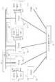
논리 검증 시스템의 대체적인 실시예가 도 2에 도시되어 있다. 이 실시예는 모든 FPGA 디바이스(22)에 병렬로 접속된 다수의 신호선(30), 및 모든 FPGA 디바이스(22)에 직렬로 접속된 데이지 체인 라인(32)을 포함하는 글로벌-이벤트-통신 버스(global-event-communication bus)를 더 포함한다. 이 실시예는 또한 도 1에 도시된 것과 같은 시스템 버스 제어기(24), 시스템 제어기(26) 및 시스템 버스(28)를 포함한다는 것을 알아야 한다. 도면을 간략화하기 위해 이 컴포넌트는 도 2에서 생략된다. 프로그램가능한 상호접속부(12)가 한정되고 비싼 자원을 구성하기 때문에 글로벌-이벤트-통신 버스가 포함된다. 프로그램가능한 상호접속부(12)를 통해서 다수의 시뮬레이션 모듈(14) 간에 공유된 신호를 라우트하기보다는, 그러한 신호는 글로벌-이벤트-통신 버스 상에서 한번에 한 신호씩 연속적으로 통신될 수 있다. 새로운 신호값의 송신기로서의 역할을 하는 시뮬레이션 모듈(14)은 그러한 신호의 일련 번호 및 그것의 새로운 값을 나타내기 위해 신호선(30)의 일부를 세트한다. 이러한 정보는 모든 다른 시뮬레이션 모듈(14)에 도달하고 필요에 따라 포획된다.An alternative embodiment of a logic verification system is shown in FIG. This embodiment is a global-event-communication bus comprising a plurality of
몇 개의 시뮬레이션 모듈(14)이 동시에 송신기로서의 역할을 할 때, 신호선(30)을 제어하게 되는 순서가 설정될 필요가 있다. 이러한 순서를 실현하기 위해, 데이지 체인 라인(32)이 토큰 링 원리에 따라 동작된다. 어떤 주어진 순간에, 데이지 체인 라인(32)의 입력부 상의 값에 의해 나타내어지는 토큰은 시뮬레이션 모듈중에서 하나와 함께 존재하여, 모듈(14)에게 신호선(30)을 제어할 수 있는 권리를 준다. 전송을 완료한 후에, 시뮬레이션 모듈(14)은 데이지 체인 라인(32) 등을 따라 다음 모듈로 토큰을 이양한다.When
시뮬레이션 모듈(14) 간에 공유된 신호를 전송하는 것에 부가적으로, 글로벌-이벤트-통신 버스도 또한 신호를 전송하여서 시뮬레이션 모듈(14)의 동작을 동기화한다. 그러한 동기화 신호의 예는 시뮬레이션 시간 진행 신호, 및 시뮬레이션 모듈(14)이 아직 현재 시뮬레이션 사이클 내에 프로세스될 몇 개의 이벤트를 갖는다는 것을 나타내는 BUSY 신호를 포함한다.In addition to transmitting a signal shared between the
행위 기술 프래그먼트를 실행하면서, 마이크로프로세서(16)는 시뮬레이션되는 논리 설계의 현재 상태를 설명하는 변수에 새로운 값을 세트할 필요가 있다. 오직 하나의 시뮬레이션 모듈(14)에 국부적으로 사용된 그러한 변수는 임의 접근 메모리 디바이스(20) 내의 적합한 위치에 의해 나타내어진다. 그러나, 행위 기술부분과 컴포넌트 상호접속부분간에 공유되고, 다수의 시뮬레이션 모듈(14) 간에 공유된 그러한 변수는 시뮬레이션 모듈(14)의 외부로 전송되어야 한다. 도 3은 마이크로프로세서 버스(18)가 다수의 어드레스 라인(34), 버스 동작(판독 또는 기록) 라인(36), 전송되는 변수를 정확하게 식별하는 코드(또는 "가변 ID")를 나타내는 다수의 데이터 라인(38), 및 그러한 변수의 새로운 값을 나타내는 데이터 라인(40)으로 분할되는 그러한 전송의 도면이다. i/o 명령의 실행 후에, 마이크로프로세서(16)는 적합한 신호값을 마이크로프로세서 버스(18)를 함께 구성하는 라인들(34-40) 상에 인스톨한다. 라인(34)과 라인(36) 상의 값의 특정의 독특한 결합은 동작 디코더(42)에 마이크로프로세서(16)가 어떤 변수의 새로운 값을 전송할 것이라는 것을 표시한다. 그 응답으로, 동작 디코더(42)는 가변 선택기(44)를 인에이블 시켜서 특정 변수의 표시로서 라인(38) 상의 값의 결합을 인식하게 한다. 그 응답으로, 가변 선택기(44)는 레지스터(46)를 인에이블하여 라인(40)으로부터의 새로운 변수값을 포획한다.While executing the behavior description fragment, the
유사하게, 행위 기술 프래그먼트를 실행하는 동안에 마이크로프로세서(16)는 논리 설계의 현재 상태가 시뮬레이션된다는 것을 기술하는 새로운 변수값을 포획할 필요가 있다. 오직 하나의 시뮬레이션 모듈(14) 내에 국부적으로 사용되는 그러한 변수는 임의 접근 메모리 디바이스(20) 내의 적합한 위치에 의해 나타내어진다. 행위 기술부분와 컴포넌트 상호접속부분간에 공유되고, 다수의 시뮬레이션 모듈(14) 간에 공유된 그러한 변수는 시뮬레이션 모듈(14)의 외부로부터 포획되어야 한다. 도 4는 FPGA(22)가 멀티플렉서(48), 중간 레지스터(50), 및 버스 구동기(52)를 부가적으로 포함할 때에 그러한 포획을 도시한다.Similarly, during execution of the behavior description fragment, the
포획 동작은 2개의 단계를 진행하며 완료시키기 위해 2개의 마이크로프로세서 명령을 수행한다. 제1 단계에서, 기록 동작이 수행된다. 동작 디코더(42)는 마이크로프로세서가 변수값을 포획하기 시작하려 한다는 표시로서 라인(34) 상의 어드레스와 라인(36) 상의 버스 동작의 결합을 인식한다. 그 응답으로, 동작 디코더(42)는 레지스터(50)를 인에이블시키고, 다음으로 라인(38) 상의 가변 ID에 기초하여 멀티플렉서(48)에 의해 선택된 변수값을 포획한다.The capture operation goes through two steps and performs two microprocessor instructions to complete. In the first step, a recording operation is performed. The
제2 단계에서 판독 동작이 수행된다. 동작 디코더(42)는 라인(34) 상의 어드레스와 라인(36) 상의 버스 동작의 결합을 마이크로프로세서가 변수값의 포획을 완료하려 하다는 표시로서 인식한다. 다음으로, 동작 디코더(42)는 버스 드라이버(52)를 인에이블시켜서 변수값을 레지스터(50)의 출력으로부터 마이크로프로세서 버스(18)의 라인(40) 상으로 전송한다.In the second step, a read operation is performed. The
상술된 바와 같이, FPGA(10, 22) 내에서 구현된 하드웨어 논리는 마이크로프로세서(16)에 의한 실행에 대한 행위 코드 프래그먼트를 선택하고 순서를 정한다. 그러한 논리의 한 실시예가 도 5에 도시되어 있다. 이 실시예는 1개 이상의 이벤트 검출기(54)(예시의 목적상, 2개가 도시됨), 이벤트 인코더(56), 및 버스 드라이버(58)를 포함한다. 각 이벤트 검출기(54)는 마이크로프로세서(16)에 의한 행위 코드의 하나의 특정 프래그먼트의 실행을 트리거하는 신호를 개별적으로 생성한다. 그 신호는 이벤트 인코더(56) 내로 공급되어서 그 출력에서 세트된 입력 신호를 정확하게 식별하는 ("이벤트 ID"라고 공지된) 코드를 제공한다.As discussed above, hardware logic implemented within
이벤트 디코더(56)로의 2개 이상의 입력이 동시에 세트되는 경우, 행위 코드 프래그먼트 실행 순서에 우선권을 갖는 이벤트의 ID를 발생시킨다. 예를 들어, 더욱 작은 이벤트 ID값을 갖는 이벤트일 수 있다.When two or more inputs to the
마이크로프로세서(16)가 다음 행위 프래그먼트를 실행할 준비가 된 경우, 판독 동작을 수행한다. 동작 디코더(42)는 라인(34) 상의 어드레스와 라인(36) 상의 버스 동작의 결합을 마이크로프로세서가 실행될 다음 행위 코드 프래그먼트의 ID를 포획하려 한다는 표시로서 인식한다. 그 응답으로, 동작 디코더는 버스 드라이버(58)를 인에이블시켜 이벤트 ID를 이벤트 인코더(56)의 출력으로부터 마이크로프로세서 버스(18)의 라인(38) 상으로 전송한다. 어떤 이벤트 검출기(54)도 행위 코드 프래그먼트의 실행을 요구하는 신호를 발생시키지 않는 경우, 이벤트 인코더(56)는 마이크로프로세서(16)에 이때에 어떤 동작도 요구되지 않는다고 표시하는 출력 신호를 발생시킨다. 적어도 하나의 이벤트 검출기(54)의 출력에서의 출력 신호의 등장은 한 실시예에서, 마이크로프로세서(16)의 방해 동작을 유발할 수 있다.When the
이벤트 ID를 마이크로프로세서(16)로 전송한 후에, 이벤트 인코더(56)는 대응하는 이벤트 검출기(54)를 자동적으로 리셋한다. 이 리셋 회로는 도면에서는 도시 생략되었으나 당분야에 공지되어 있으며, 당분야의 업자에 의해 용이하게 재생될 수 있다.After sending the event ID to the
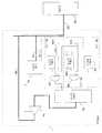
이벤트 ID 계산 논리의 다른 실시예가 도 6에 도시되어 있다. 이 실시예에서, 이벤트 검출기(54)는 행위 모델의 스케줄 요구에 따라 그룹화될 수 있다. 예를 들어, Verilog 하드웨어 기술 언어로 작성된 모델에 대해서 그러한 유구가 I.E.E.E. 드래프트 표준 1364의 5장에 정의되어 있다. 특히, Verilog 모델은 동일한 시뮬레이션 사이클 내에서 프로세스된 모든 이벤트가 4개의 그룹으로, 즉, 활성 이벤트들(active event), 비활성 이벤트들(inactive event), 비-블록킹 할당 업데이트 이벤트들(non-blocking assign update event), 및 모니터 이벤트들(monitor event)로 그룹화될 것을 요구한다. Verilog 모델은 또한 활성 이벤트, 비활성 이벤트, 비-블록킹 할당 업데이트 이벤트, 그리고 모니터 이벤트의 순서로 프로세스될 것을 요구한다.Another embodiment of the event ID calculation logic is shown in FIG. 6. In this embodiment, the
이러한 요구에 부합하기 위해, 도 6에 도시된 실시예는 다수의 이벤트 검출기의 그룹을 포함한다. 각 그룹은 하나 이상의 이벤트 검출기(54)(예로서, 각 그룹에 하나씩 도시됨), 및 AND 게이트(60)를 갖는다(예외, 제1 그룹은 그런 AND 게이트(60)를 포함하지 않음). 제2 그룹에 속하는 AND 게이트(60)는 제1 그룹에 프로세스되지 않은 이벤트가 있다는 것을 표시하는 BUSY[1] 신호(62a)에 의해 제어된다. 유사하게, 제3 그룹의 AND 게이트(60)는 BUSY[1] 신호(62a), 및 여전히 제2 그룹 내에 프로세스되지 않은 이벤트가 있다는 것을 표시하는 BUSY[2] 신호(62b)에 의해 제어된다. 그 결과, 제1 그룹 내에 어떤 두드러진 이벤트가 없는 경우에 한하여 제2 그룹에 속하는 이벤트 검출기(54a)로부터의 신호가 이벤트 인코더(56)에 도달하게 될 것이다. 유사하게, 제1 또는 제2 그룹에 어떤 두드러진 이벤트가 없는 경우에 한하여 제3 그룹에 속하는 이벤트 검출기(54b)로부터의 신호가 이벤트 인코더(56)에 도달하게 된다. 이 패턴은 필요에 따라 더욱 많은 BUSY 신호(62)를 이용하여 제4 및 그 이상의 그룹에 대해서 지속한다.To meet this need, the embodiment shown in FIG. 6 includes a group of multiple event detectors. Each group has one or more event detectors 54 (eg, one shown in each group), and an AND gate 60 (except, the first group does not include such an AND gate 60). AND
BUSY 신호들(62)의 형성이 도 7에 도시되어 있다. 각 BUSY 신호(62)는 대응하는 그룹에 속하는 모든 이벤트 검출기(54)의 출력 신호의 논리 OR 함수(64)로서 형성된다. 구체적으로 BUSY[1] 신호(62a)가 제1 그룹의 이벤트 검출기를 이용하여 형성되고, BUSY[2] 신호(62b)가 제2 그룹의 이벤트 검출기를 이용하여 형성되는 등등이다. 모든 시뮬레이션 모듈들(14)로부터의 그룹 내의 모든 이벤트 검출기(54)로부터의 출력은 BUSY 신호(62)를 형성하기 위해 모두 OR되어야 한다. 본 발명의 한 실시예에서, BUSY 신호(62)를 형성하기 위해 포선 논리가 사용되어서, OR 함수(64)가 배선으로 암시적으로 구현되어 있다. 그러나, 다른 실시예에서, 글로벌-이벤트-통신 버스 라인들(30)의 일부가 모든 시뮬레이션 모듈(14) 중에 BUSY 신호(62)를 전파시키기 위해 사용되었다.The formation of
어떠한 BUSY 신호(62)도 표명되지 않는 경우, 현재 시뮬레이션 사이클이 완료된다. 그러한 완료를 검출하고 시뮬레이션을 다음 사이클로 진행시키는 회로가 도 8에 도시되어 있다. 회로는 사용된 BUSY 신호(62)의 개수에 상응하는 개수의 입력을 갖는 NOR 게이트(66), 및 카운터(68)로 구성되어 있다. 비록 4개의 BUSY 신호(62)가 NOR(66)로의 입력으로 도시되었으나, 몇 개의 BUSY 신호(62)라도 채택될 수 있다는 것이 알아야 한다. 어떤 BUSY 신호도 표명되지 않는 경우, NOR 게이트(66)는 카운터(68)의 동작을 인에이블시킨다. 이 카운터는 논리 검증 시스템 내부를 비동기적으로 및 연속적으로 실행시키는 고속 주기적 클럭 신호(70)에 의해 클럭된다. 클럭의 주파수는 시스템 내의 신호 트랜지스터의 주파수보다 높아야 한다. BUSY 신호(62)의 가장 긴 전파 지연에 대한 보상을 위해 필요한 클럭 신호(70) 상의 클럭 사이클의 개수를 카운트한 후에, 카운터(68)는 모든 시뮬레이션 모듈(14)에 전파되는 시간 선행 신호(time advance signal)(72)를 발생시키면서 오버플로우한다. 본 발명의 한 실시예에서, 글로벌-이벤트-통신 버스 라인(30)은 모든 시뮬레이션 모듈(14) 중에서 시간 선행 신호를 전파하는데 사용된다.If no
도 9는 공유된 멀티플렉스된 버스(82) 상에서 한 FPGA(22)로부터 다른 FPGA로의 이벤트의 전송을 상세하게 보여준다. 이 데이터 전송 방법은 프로그램가능한 상호접속부(12)의 가치 있는 자원의 보전하기 위해 본 발명의 한 실시예에서 사용된다.9 details the transfer of events from one
전송 FPGA(22)(도 9의 좌측)는 이벤트 인코더(56)와 그 기능성에 있어서 유사한 제2 이벤트 인코더(74)를 포함한다. 이 전송 FPGA(22)는 (버스 드라이버(58)와 유사한) 버스 드라이버(76) 및 전송 제어기(78)를 더 포함한다. 전송 제어기(78)가 버스 중재 입력 신호(80)를 검출할 때, 이벤트 인코더(74)가 다수의 이벤트 검출기들(54)로부터의 입력에 어떤 활성 신호를 갖는가를 체크한다. 그러한 신호가 존재할 때, 버스 드라이버(76)를 통해서 공유 멀티플렉스된 버스(82) 상에 제1 이벤트 ID의 전송을 인에이블시킨다. 버스(82)의 가장 긴 전파 지연에 대해서 보상하기 위해 필요한 고속 주기적 클럭 신호(70)(도시 생략)의 다수의 사이클 후에, 전송 제어기(78)는 이미 전송된 이벤트에 상응하는 이벤트 검출기(54)를 리셋하고, 소정의 순서로 다음 이벤트를 등장시키기 위해 이벤트 인코더(74)에 신호를 전송한다. 모든 이벤트를 전송한 후에, 전송 제어기(78)는 버스 드라이버(76)를 디스에이블하고 버스 중재 출력 신호(84)를 표명하고, 이에 따라 버스(82)에 대한 제어를 포기한다. 한 시뮬레이션 모듈(14)의 버스 중재 출력 신호(84)는 데이지 체인을 형성하기 위해 다른 시뮬레이션 모듈(14)의 버스 중재 입력 신호(80)에 접속된다.Transmit FPGA 22 (left of FIG. 9) includes an
FPGA(22)(도 9의 우측)를 수용함에 있어서, 공유 멀티플렉스된 버스(82)는 이벤트 ID 라인(88), 변수값 라인(86), 및 이벤트 준비 라인(90)으로 분할된다. 이벤트 준비 신호(90)의 검출 중에, 가변 선택기(92)는 라인(88) 상의 값의 결합을 특정 변수의 표시로서 인식한다. 그 응답으로, 가변 선택기(92)는 레지스터(46)를 인에이블하여 라인(86)으로부터의 변수의 새로운 값을 포획한다.In accommodating the FPGA 22 (right side of FIG. 9), the shared multiplexed
본 발명의 한 실시예에서, 글로벌-이벤트-통신 버스 라인(30)이 공유 멀티플렉스된 버스(82)를 구현하는데 사용되고 데이지 체인(32)의 선택이 버스 중재 신호들(80, 84)을 구현하기 위해 사용된다.In one embodiment of the invention, global-event-
도 10은 이벤트 검출기(54)의 양호한 실시예를 상세하게 설명한다. 이벤트 검출기는 하나 이상의 입력 및 하나의 출력을 갖는 조합 논리 블럭(98)을 포함한다. 블럭(98)의 하나 이상의 입력은 변수값을 나타내는 신호에 직접 접속될 수 있다. 블럭(98)의 다른 입력은 다른 결합 블럭들(94) 및 에지 검출기(96)를 통해서 변수값을 나타내는 신호에 접속될 수 있다. 에지 검출기(96)는 그 입력 신호의 포지티브 에지(positive edge), 네거티브 에지(negative edge), 또는 임의의 에지를 검출한다. 에지 검출기의 구성은 도시 생략되었으나 당분야의 업자에 의해 용이하게 재생될 수 있으며, 당분야에 공지되어 있다.10 describes in detail the preferred embodiment of the
도 10에 도시된 바와 같이, 결합 블럭(98)의 출력은 플립/플롭(102)의 "세트" 입력에 직접 또는 지연 카운터(100)를 통해서 접속된다. 후자의 경우, 조합 논리 블럭(98)의 출력 신호는 시간 선행 신호(72)에 의해 클럭된 지연 카운터(100)를 인에이블시킨다. 소정의 개수의 시간 선행 신호(72)를 카운트한 후에, 카운터(100)는 오버플로우하고 이벤트 검출기(54)의 출력에서 신호를 발생시킨다. 이벤트 출력이 전송된 후에, 상술된 이벤트 인코더(56)에 의해 리셋 라인(101)을 이용하여 이벤트 검출기(54)가 리셋된다.As shown in FIG. 10, the output of the
도 10에 도시된 일반적인 구조는 (조합 논리 블럭(98) 만을 이용하여) 임의 레벨 감응 이벤트 제어(arbitrary level sensitive event control)를, 또는 (결합 블럭들(94) 및 에지 검출기(96)를 사용하여) 에지 감응 이벤트 제어를, 또는 (지연 카운터(100)를 이용하여) 지연을, 또는 그것의 조합을 구현할 수 있다. 각 특정 이벤트 검출기(54)는 필요에 따라 그러한 기능 모두 또는 일부를 가질 수 있다.The general structure shown in FIG. 10 uses arbitrary level sensitive event control (using only combinational logic block 98), or (using combination blocks 94 and edge detector 96). Edge sensitive event control, or delay (using delay counter 100), or a combination thereof. Each
일반적으로 에뮬레이션 기술은 다양한 입력 및 출력 신호 이벤트사이의 정확한 시간 간격을 계산하는 의미에서 설계의 실제 타이밍의 검증을 위해 적합하지 않다. 따라서, 서로에 대한 데이터 의존성을 갖는 상이한 회로 컴포넌트의 교정 평가 순서를 보장하는 방법으로서만 교정 모델 타이밍은 중요하다. 이러한 타이밍 교정 문제의 가장 중요한 경우는 유지 시간 위반이 가능한 플립/플롭의 체인의 평가이다. 어떤 클럭된 디바이스에 대해서도 특정된 "셋업 타임" 및 "유지 시간"이 있다. 셋업 타임은 입력 데이터가 플립-플롭 디바이스의 데이터 입력 리드(data input lead)에서 클럭 전이 이전에 소정의 시간량에 대한 안정적인 형태로 나타나야할 것을 요구한다. 유지 시간은 데이터가 플립-플롭의 제어 리드에 도달하는 클럭 전이의 시점으로부터 적합한 동작에 대한 클럭의 도달 후에 특정의 시간 간격까지 안정하게 될 것을 요구한다. 사용자의 넷리스트로부터 논리 회로를 구현하는 핵심 프로세스는 데이터의 셋업 및 유지 시간을 상응하는 클럭의 도달과 동기화시키는 것이다. 구현된 논리 회로의 적합한 동작을 보장하기 위해 클럭 입력에서 상응하는 클럭의 도달에 대하여 시간의 특정 간격 동안에 플립-플롭의 D 입력에서 데이터가 나타나고 안정화하여야 한다. 사용자의 넷리스트로부터 회로를 구현함에 있어서, 클럭 신호의 적합한 타이밍이 클럭 스큐(skew)를 원인으로 하여 클럭 라인내의 과도한 지연으로 인해 방해받을 수 있다. 이것은 플립-플롭 또는 시프트 레지스터 같은 제1 논리 디바이스 내의 데이터가 제2 레지스터 상의 데이터보다 더 일찍 시프트되도록 유발한다. 제2 레지스터의 유지 시간 요구는 위반되고 이어서 데이터 비트는 시프트 레지스터가 적합하게 동기화되지 않는 한 유실될 수 있다.In general, emulation techniques are not suitable for verifying the actual timing of a design in the sense of calculating the exact time interval between various input and output signal events. Thus, calibration model timing is important only as a method of ensuring the calibration evaluation order of different circuit components having data dependencies on each other. The most important case of this timing correction problem is the evaluation of the chain of flips / flops, which can lead to retention time violations. There is a "setup time" and "hold time" specified for any clocked device. The setup time requires that the input data appear in a stable form for a predetermined amount of time before the clock transition in the data input lead of the flip-flop device. The hold time requires that the data be stable from a point in time of the clock transition that reaches the control lead of the flip-flop until a certain time interval after the arrival of the clock for proper operation. The key process for implementing logic circuitry from the user's netlist is to synchronize the setup and maintenance time of the data with the arrival of the corresponding clock. To ensure proper operation of the implemented logic circuit, data must appear and stabilize at the D input of the flip-flop during a certain interval of time with respect to the arrival of the corresponding clock at the clock input. In implementing circuitry from the user's netlist, proper timing of the clock signal may be hindered by excessive delay in the clock line due to clock skew. This causes the data in the first logical device, such as a flip-flop or shift register, to shift earlier than the data on the second register. The hold time requirement of the second register is violated and the data bits may then be lost unless the shift register is properly synchronized.
유지 시간 위반은 그 위반이 에뮬레이션 회로의 의도적 생성물이 아니기 때문에 목표 시스템 또는 최종 제품에서는 발생하지 않는다. 이것은 재프로그램가능한 논리 디바이스내의 한정된 자원이 클럭 신호의 발생을 지원하도록 설계되었으므로 유지 시간 위반이 목적 시스템 내의 클럭 스큐와 종종 상이한 에뮬레이션 회로 내의 클럭 스큐로부터 유래하기 때문이다. 논리 검증 시스템 내의 행위 시뮬레이션은 시뮬레이션된 그리고 에뮬레이션된 회로 컴포넌트가 공존할 것을 요구하기 때문에, 양 기술에서의 타이밍 교정을 위해 호환성 있는 수단이 사용되는 것은 중요하다.The retention time violation does not occur in the target system or the final product because the violation is not an intentional product of the emulation circuit. This is because the hold time violation comes from a clock skew in an emulation circuit that is often different from the clock skew in the target system because the limited resources in the reprogrammable logic device are designed to support the generation of the clock signal. Because behavioral simulations within a logic verification system require simulated and emulated circuit components to coexist, it is important that compatible means be used for timing correction in both techniques.
시뮬레이션 기술, 모델 타이밍이 지연 및 비-블록킹 할당 명령문 같은 적합한 언어 구성 요소에 의해 기술된다. 타이밍은 그러한 구성 요소의 어의가 시뮬레이터에 의해 정확하게 번역되는 한 정의에 의해 정확하다. 이것은 실제의 지연값이 미지라고 추정되는 경우 제로-지연 시뮬레이션의 경우에서도 참이다. 예를 들어, 2개의 플립/플롭각각은 평가의 정확한 순서를 보장할 Verilog 하드웨어 기술 언어 내의 다음의 행위 코드로써 정의될 수 있다.Simulation techniques, model timing are described by suitable language components, such as delay and non-blocking assignment statements. Timing is accurate by definition, as long as the semantics of such components are translated correctly by the simulator. This is true even in the case of zero-delay simulation when the actual delay value is assumed to be unknown. For example, two flips / flops each can be defined as the following behavior code in the Verilog hardware description language that will ensure the correct order of evaluation.
always @ (postage clk)always @ (postage clk)
q = #0 d; q = # 0 d;
또는or
always @ (postage clk)always @ (postage clk)
q < = d;q <= d;
명시적 지연, 제로 지연, 및 비-블록킹 할당의 해석은 상이한 시뮬레이션 사이클들로의 또는 동일한 사이클 내의 상이한 그룹들로의 이벤트의 할당에 기초한다. 이러한 이벤트 할당은 행위 설계부에 대한 언어 어의에 의해 함축된 이벤트 순서를 강제하게 한다.The interpretation of explicit delay, zero delay, and non-blocking assignment is based on the assignment of an event to different simulation cycles or to different groups within the same cycle. This event assignment causes the sequence of events implied by the language semantics to the behavior design unit.
그러나, 에뮬레이션 기술에 있어서, 직렬 접속 플립/플롭의 쌍은 다음과 같이 기술된다.However, in the emulation technique, the pair of serially connected flip / flops is described as follows.
always @ (posedge clk1)always @ (posedge clk1)
q1 = #t1 d1; q1 = # t1 d1;
always @ (posedge clk2)always @ (posedge clk2)
q2 = #t2 d2; q2 = # t2 d2;
assign #td d2 = q1;assign #td d2 = q1;
assign #tc clk2 = clk1;assign #tc clk2 = clk1;
(모든 에뮬레이션 회로 지연(t1, t2, td, 및 tc)이 공지되어 있으나 상한 T를 갖는다.) 교정 평가 순서를 보장하기 위해, 에뮬레이션은 T만큼 td의 값을 증가시킨다. 에뮬레이터는 또한 (클럭 트리(clock tree)의 공통 부분의 특별 FPGA 디바이스 및 클럭 논리의 복제로의 분리 같은) 회로 변환을 구현하여서 T의 값이 가능한 한 작게 된다. 이 프로세스는 첸 등의 1995년 12월 12일 출원된 미국 특허 제5,475,830호 "Structure and Method for Providing a Reconfigurable Emulation Circuit without Hold Time Violation"(퀵턴 시스템사(Quickturn Systems, Inc.)에 양도)에 설명되어 있다.(All emulation circuit delays t1, t2, td, and tc are known but have an upper limit T.) To ensure calibration evaluation order, the emulation increases the value of td by T. The emulator also implements circuit transformations (such as the separation of special FPGA devices and clock logic from a common part of the clock tree) so that the value of T is as small as possible. This process is described in US Pat. No. 5,475,830, filed December 12, 1995, entitled "Structure and Method for Providing a Reconfigurable Emulation Circuit without Hold Time Violation" (transferred to Quickturn Systems, Inc.). It is.
타이밍 교정을 보장하는 각 방법은 그 자신의 도메인 내에서 호환성이 있다. 그러나, 에뮬레이션과 시뮬레이션 모델의 혼합은 문제를 발생시킬 수 있다. 예를 들어, 체인 내의 제2 플립/플롭, 또는 그 클럭 논리의 어떤 부분이 에뮬레이션 모델로서보다는 제로-지연 행위(즉, 시뮬레이션 모델)로서 기술될 가능성을 고려하자. 이러한 경우에 지연값의 상한 T가 결정될 수 없으며 전형적인 에뮬레이터에 의해 사용된 타이밍 교정을 보장하는 방법이 작동하지 않은 것이다.Each method of ensuring timing correction is compatible within its own domain. However, mixing emulation and simulation models can cause problems. For example, consider the possibility that a second flip / flop, or any portion of its clock logic, in the chain may be described as a zero-delay behavior (ie, a simulation model) rather than as an emulation model. In this case the upper limit T of the delay cannot be determined and the method of guaranteeing the timing correction used by a typical emulator has not worked.
유지 시간 위반을 제거하는 해결방법은 각 에뮬레이션 플립/플롭의 데이터경로를 따라 부가적인 플립/플롭 업스트림을 배치하게 한다. 이러한 방법의 예가 프라이스 등의 1993. 11. 2.에 출원된 미국 특허 제5,259,006호 "Method for Substantially Eliminating Hold Time Violation in Implementing High Speed Logic Circuits or the like"에 보여진다. 그러나, 이 방법은 부가적인 플립/플롭이 삽입될 필요가 있는가를 결정하기 위해 각 행위 블록이 플립/플롭 또는 조합 회로로서 분류될 것을 요구하기 때문에 행위 검증 시스템에 적용하기에는 어렵거나 불가능하다. 또한 그러한 블럭의 각 입력이 데이터 입력 또는 클럭 입력으로서 식별할 필요가 있다. 그러한 식별은 하드웨어 기술 언어의 제약 조건으로 인해 어렵거나 불가능하다. 부가적인 플립/플롭이 조합 논리 블럭의 업스트림에 배치되는 경우 설계자가 의도한 행위를 변경할 수 있다.The solution to eliminate hold time violations allows placing additional flip / flop upstream along the datapath of each emulation flip / flop. An example of such a method is shown in US Pat. No. 5,259,006, entitled "Method for Substantially Eliminating Hold Time Violation in Implementing High Speed Logic Circuits or the like," filed November 11, 1993, to Price et al. However, this method is difficult or impossible to apply to an action verification system because it requires each action block to be classified as a flip / flop or combination circuit to determine if additional flip / flops need to be inserted. In addition, each input of such a block needs to be identified as a data input or clock input. Such identification is difficult or impossible due to the constraints of the hardware description language. If additional flip / flops are placed upstream of the combinational logic block, the designer can change the intended behavior.
본 발명에 의해 제공되는 한 방법은 상이한 종류의 지연-무관 유지 시간 위반 제거 방법(delay-independent hold-time violation elimination)이다. 도 11에 도시된 바와 같이, 유지 시간 위반을 갖는 어떤 다른 회로 컴포넌트(106)에 잠재적으로 도달할 수 있는 신호의 소스인 각 플립/플롭(104)에 대해서, 부가적인 플립/플롭(108)이 다운스트림으로 삽입된다. 시뮬레이션 클럭(110)은 모든 BUSY 신호들(62)이 표명되지 않은 때에 표명된다. 그 결과, 플립/플롭(104)으로부터 유래한 데이터경로(112) 내의 효과적인 지연은 플립/플롭(104)이 에뮬레이션되었는지 또는 시뮬레이션되었는지 여부에 상관없이 플립/플롭(104)의 클럭 신호(116)와 플립/플롭(106)의 클럭 신호(118)를 분리시키는 결합 클럭 경로(114) 내의 지연보다 항상 더 크다.One method provided by the present invention is a different kind of delay-independent hold-time violation elimination. As shown in FIG. 11, for each flip /
더 복잡한 상황이 도 12에 도시되어 있는데, 에뮬레이션된 플립/플롭(120)이 클럭 회로(122) 내에 존재한다. 회로(122)의 지연이 회로(112)의 지연보다 적다는 것이 설계 의도였다고 가정하면, 부가적인 플립/플롭이 클럭 회로(122) 내에 삽입되지 않아야 한다. 플립/플롭(120)에 의해 발생된 신호가 다른 플립/플롭(126)에 대한 데이터 소스로서도 사용되었을 경우, 이에 따라 도 12에 도시된 바와 같이 부가적인 플립/플롭(124) 및 회로(128)와 같은 회로(122)의 복제가 필요하다. 이전에 회로(122)를 플립/플롭(126)과 접속시키는 신호(130)는 제거되어야 한다. 이러한 변환이 정확하게 적용되도록 하기 위해, 클럭 회로 분석이 수행되어서 어떤 클럭 에지가 (에뮬레이션된 또는 시뮬레이션된) 각 저장 엘리먼트의 클럭 입력상에 잠재적으로 활성화될 수 있는가를 결정할 필요가 있다. 행위 블럭에 대해서, 외부 플립/플롭이 유지 시간 위반의 위험에 처해있다고 잘못 식별할 때일지라도 변환이 검증 하의 회로에 의해 수행된 기능을 대체시키지 않을 것이기 때문에 그 저장기능이 적용될 것인지에 대해 신중한 가정이 이루어진다. 최악의 경우 회로의 에뮬레이션된 부분 내의 각 플립/플롭은 시뮬레이션 클럭 신호(110)에 의해 동기화된 플립/플롭으로 복제되어야 한다.A more complex situation is shown in FIG. 12, where emulated flip /
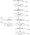
도 13은 논리 검증 시스템에 의해 사용될 구성 데이터를 준비하는 플로우 다이어그램이다. 일반적으로, 컴파일화는 예를 들어 Verilog 하드웨어 기술 언어("Verilog HDL") 내의 사용자의 설계 기술 파일로부터 시작한다. 그러나, 컴파일레이션은 다양한 다른 언어들로써 시작할 수 있다. 입력 단계(132)의 결과로서, 행위 데이터베이스 기술(134)이 생성된다. 이 기술은 다른 행위 기술(138)을 발생시키는 전처리 단계(136)에 의해 증대된다. 넷리스트 발생 단계(140) 및 코드 발생 단계(144)는 에뮬레이션 모델의 넷리스트 기술(142) 및 논리 모듈 프로세서 메모리(20)에 다운로드될 수 있는 실행의 세트(146)를 발생시킨다. 이 넷리스트 기술(142)은 분할(partitioning), 위치(placement), 및 라우팅 단계(148)를 거치게 되어 FPGA(10, 22) 및 프로그램가능한 상호접속(12)에 대한 구성 데이터(150)를 발생시킨다. 이 분할, 배치, 라우팅 단계는 샘플 등의 미국 특허 제5,329,470호 및 버츠 등의 제5,036,473호에 기술되어 있으며 당분야의 업자에게 공지되어 있다.13 is a flow diagram for preparing configuration data for use by a logic verification system. In general, compilation starts with a user's design description file, for example in Verilog hardware description language ("Verilog HDL"). However, compilation can be started in a variety of other languages. As a result of the
보다 구체적으로, 입력(132)은 사용자의 Verilog 소스 파일을 프로세스하고 행위 데이터베이스 라이브러리를 발생시킨다. 그것은 소스 파일명의 리스트, "인클루드(include)" 경로 및 다른 정의되지 않은 모듈 참조가 해결된 탐색 라이브러리의 리스트를 수용한다. 임포터는 행위 기술은 동시에 실행가능한 코드 프래그먼트들로 분할한다.More specifically, input 132 processes the user's Verilog source file and generates an action database library. It accepts a list of source file names, an "include" path, and a list of search libraries in which other undefined module references are resolved. The importer splits the behavior description into executable code fragments at the same time.
전처리기(136)는 입력 단계(132)에 의해 생성된 행위 데이터베이스 라이브러리를 변환시킨다. 그것은 행위 코드를 사용가능한 모듈(14) 각각 상에서 실행을 지향하는 클러스터로 분할하고, 행위 코드 프래그먼트의 실행 순서 및 구획내의 변수의 국부성을 결정한다. 또한, 전처리기(136)는 상술된 유지-시간위반-자유 모델(hold-time-violation-free model)을 생성하는데 필요한 변환을 수행한다.
코드 발생기(144)는 전처리기(136)에 의해 변환된 만큼의 행위 데이터베이스 라이브러리를 판독하고 전처리기(136)에 의해 식별되는 만큼의 시뮬레이션 모듈들(14) 각각에 대해서 다운로딩가능한 실행가능물(executable)(146)을 발생시킨다.The
넷리스트 발생기(140)는 전처리기(136)에 의해 변환된 만큼의 행위 데이터베이스 라이브러리를 판독하고 분할, 위치, 및 라우팅 단계(148)에 의한 또 다른 프로세싱을 위해서 넷리스트 데이터베이스 라이브러리를 발생시킨다.
논리 검증 시스템의 동작은 당분야의 업자에게 공지된 이벤트-중심 시뮬레이션의 원리에 기초한다. 기본적 가정은 다음과 같다: (1) 어떤 주어진 행위 모델은 평가 프로세스의 세트로 분할될 수 있어서, 행위 기술에 기초하여 컴파일된다; (2) 시뮬레이션의 프로세스는 어떤 변수(입력)의 논리값을 판독하고 다른 변수(출력)의 새로운 값을 계산하는 상기 절차의 일련의 실행가능으로 구성된다; (3) 상기 절차는 시뮬레이션 모델의 현재 상태에 따라 각 절차를 실행할 것인가를 결정하는 할당된 트리거링 조건이다.The operation of the logic verification system is based on the principles of event-driven simulation known to those skilled in the art. The basic assumptions are as follows: (1) Any given behavior model can be broken down into a set of evaluation processes, compiled based on the behavior description; (2) the process of simulation consists of a series of executables of the above procedure of reading the logical value of one variable (input) and calculating a new value of another variable (output); (3) The procedure is an assigned triggering condition that determines whether to execute each procedure according to the current state of the simulation model.
예를 들어, 도 14에 도시된 Verilog HDL 모델을 고려하자. 이 모델은 Q_ AN02로 시작하는 10개의 평가 프로세스들로 구성된다. 이 절차중의 9개는 라이브러리 프리머티브(Q_AN02 및 Q_FDP0)를 참조로 하여 사전 정의되고 하나는 행위 기술로써 표현된다. 평가 프로세스간의 이러한 관계는 도 15에 도시된 바와 같이 그래프로 설명될 수 있다.For example, consider the Verilog HDL model shown in FIG. This model consists of 10 evaluation processes starting with Q_ AN02. Nine of these procedures are predefined with reference to the library primitives Q_AN02 and Q_FDP0 and one is represented as an action description. This relationship between the evaluation processes can be described graphically as shown in FIG. 15.
에뮬레이션의 목적상, 인스턴스(U1 및 m0-m7)는 FPGA 내에서 직접 수행될 수 있다. 인스턴스 라인_선택(instance line_select)의 출력을 평가하는 행위 코드는 내장 마이크로프로세서에 대한 명령의 시퀀스로서 컴파일된다. 이 시퀀스가 적합한 시간에 호출되도록 하기 위해서는 유일한 ID가 하나의 마이크로프로세서 내에 로드된 그러한 시퀀스 각각에 할당되어야 한다. ID는 상응하는 트리거링 조건이 참이 되는 경우 FPGA 내에서 발생될 수 있다. (ID을 발생시키는 회로는 도 5에 상술되었다.) 동시에 몇 가지 트리거링 조건이 참이 되는 경우, 그의 ID중에서 가장 작은 것이 발생된다. 마이크로프로세서(16)는 ID을 지속적으로 모니터하고, 새로운 ID가 발생될 때마다, 상응하는 명령 시퀀스가 실행된다. 라인_선택 기능의 ID가 5라고 가정하면, 이벤트-발생 논리는 도 16에 도시된 바와 같이 수행될 수 있다. (고속 주기적 신호에 의해 동기화된) CLK의 네거티브 에지가 검출되는 경우, 이벤트 검출기(152) 내의 RS-트리거를 세트한다. 5 이하의 ID를 갖는 이벤트가 전혀 없는 경우, 이에 따라 이벤트 인코더(154)는 번호 5를 발생시키고 마이크로프로세서(16)는 FPGA 어드레스 공간에 속하는 어드레스중의 하나로부터 판독 명령이 실행되는 경우 번호 5를 검출한다. 이때 RS 트리거가 리셋된다(동작 디코더, 버스 드라이버 및 데이터 레지스터는 도시 생략).For the purposes of emulation, instances U1 and m0-m7 can be performed directly within the FPGA. The act code evaluating the output of the instance line_select is compiled as a sequence of instructions for the embedded microprocessor. In order for this sequence to be called at the appropriate time, a unique ID must be assigned to each such sequence loaded in one microprocessor. An ID can be generated within the FPGA if the corresponding triggering condition is true. (The circuit that generates the ID has been described above in Fig. 5) At the same time, when several triggering conditions become true, the smallest of the IDs thereof is generated. The
동작 방법은 다음과 같이 요약될 수 있다. 모델 컴파일 시에, 행위 코드들로써 나타내어지는 셀(예, 도 15의 라인_선택 셀)이 그의 상응하는 이벤트 발생 논리 블록들(도 16에 도시된 것과 유사)로 교체된다. 실행 시에, 마이크로프로세서(16)는 FPGA로부터의 다음 이벤트의 ID의 판독, 및 이러한 이벤트에 상응하는 기능의 실행으로 구성된 루프 내에서 지속적으로 실행한다. 이러한 동작을 수행하기 위해 마이크로프로세서(16)에 의해 사용될 수 있는 프로그램의 예가 도 17에 도시되어 있다.The method of operation can be summarized as follows. Upon model compilation, the cell represented by the behavior codes (eg, the line_selection cell of FIG. 15) is replaced with its corresponding event generation logic blocks (similar to that shown in FIG. 16). At execution time, the
시뮬레이션 알고리즘의 이러한 소프트웨어-하드웨어 구현은 레벨화된 그리고 이벤트-중심 시뮬레이션의 최상의 특성을 결합시킨다. 이벤트-중심 시뮬레이션에서와 같이, 오직 그러한 프리머티브만이 활성화 조건이 만족되는 각 사이클에서 평가된다. 레벨화되고 컴파일된 시뮬레이션에서와 같이, 이벤트 큐 조작의 오버헤드가 모델 실행 단계로부터 제거된다. 모든 필요한 이벤트 검출 및 조작이 재구성가능한 하드웨어(FPGA) 내에서 구현된다. 이벤트 검출 하드웨어 넷리스트는 모델 분할 및 정렬의 결과뿐아니라, 각 평가된 루틴에 대해서 트리거 조건에 기초하여 컴파일 시에 생성된다.This software-hardware implementation of the simulation algorithm combines the best features of leveled and event-driven simulation. As in event-driven simulation, only such primitives are evaluated in each cycle where the activation condition is met. As with the leveled and compiled simulations, the overhead of event queue manipulation is removed from the model execution phase. All necessary event detection and manipulation is implemented in reconfigurable hardware (FPGA). Event detection hardware netlists are generated at compile time based on trigger conditions for each evaluated routine as well as the results of model partitioning and sorting.
본 발명의 상기 실시예가 설명되었으나, 당분야의 업자라면 본 발명의 사상 또는 범위로부터 벗어나지 않고 수많은 변화가 이루어질 수 있다는 것이 명백할 것이다. 상기 설명 내에 포함되고 첨부 도면내에 도시된 모든 것은 설명을 위한 것이며 발명을 한정하는 것은 아닌 것으로 해석되어야 한다. 따라서, 본 발명은 청구범위에 의해서만 한정될 것이다.While the foregoing embodiments of the invention have been described, it will be apparent to those skilled in the art that numerous changes may be made without departing from the spirit or scope of the invention. All things included in the above description and shown in the accompanying drawings are to be interpreted as illustrative and not restrictive. Accordingly, the invention will be limited only by the claims.
도 1은 다수의 프로세서 및 프로그램가능한 게이트 어레이 디바이스를 갖는 논리 검증 시스템의 한 실시예의 블럭 다이어그램.1 is a block diagram of one embodiment of a logic verification system having multiple processors and a programmable gate array device.
도 2는 글로벌-이벤트-전송 버스를 포함하는 논리 검증 시스템의 다른 실시예의 블럭 다이어그램.2 is a block diagram of another embodiment of a logic verification system including a global-event-transmission bus.
도 3은 시뮬레이션된 설계부분으로부터 에뮬레이션된 설계부분 내로의 변수의 계산된 값의 전송의 블럭 다이어그램.3 is a block diagram of the transfer of a calculated value of a variable from a simulated design portion into an emulated design portion.
도 4는 에뮬레이션된 설계부분으로부터 시뮬레이션된 설계부분 내로의 변수의 계산된 값의 포획의 블럭 다이어그램.4 is a block diagram of the capture of a calculated value of a variable from an emulated design portion into a simulated design portion.
도 5는 이벤트 코드의 계산 및 행위 시뮬레이션을 수행하는 마이크로프로세서로의 전송의 블럭 다이어그램.5 is a block diagram of transmission to a microprocessor for performing calculation of event codes and simulation of behavior.
도 6은 이벤트가 예를 들어, 활성 이벤트, 비활성 이벤트, 비-블록킹 할당 업데이트 이벤트, 및 모니터 이벤트들로 그룹화할 때 이벤트 코드의 계산 및 행위 시뮬레이션을 수행하는 마이크로프로세서로의 전송을 도시하는 다른 실시예의 블럭 다이어그램.FIG. 6 is another implementation showing transmission to a microprocessor that performs calculations and simulations of event codes when events are grouped into, for example, active events, inactive events, non-blocking allocation update events, and monitor events. Example block diagram.
도 7은 이벤트 그룹내의 두드러진 이벤트의 검출의 블럭 다이어그램.7 is a block diagram of detection of salient events in an event group.
도 8은 시뮬레이션 시간을 선행시키는 신호의 계산을 설명하는 블럭 다이어그램.8 is a block diagram illustrating the calculation of a signal that precedes the simulation time.
도 9는 공유 멀티플렉스된 버스 상에서 한 마이크프로세서로부터 다른 마이크로프로세서로의 이벤트의 전송의 도면.9 is a diagram of the transmission of events from one microprocessor to another on a shared multiplexed bus.
도 10은 이벤트 검출기의 블럭 다이어그램.10 is a block diagram of an event detector.
도 11은 설계의 에뮬레이션 동안에 유지 시간 위반을 방지하기 위해 검증 하에서 논리 설계에 대해서 고안된 한 변환의 블럭 다이어그램.11 is a block diagram of a transform designed for a logic design under validation to prevent retention time violations during emulation of the design.
도 12는 설계 에뮬레이션 동안에 유지 시간 위반을 방지하기 위해 논리 설계에 대해서 고안된 다른 변환의 블럭 다이어그램.12 is a block diagram of another transformation designed for a logic design to prevent hold time violations during design emulation.
도 13은 논리 검증 시스템의 프로그래밍의 블럭 다이어그램.13 is a block diagram of the programming of a logic verification system.
도 14는 Verilog 하드웨어 기술 언어 내의 코드 프래그먼트를 사용하여 부분적으로는 컴포넌트 상호접속에 의해, 그리고 부분적으로는 행위 기술에 의해 표현된 논리 설계의 예의 도면.14 is a diagram of an example of a logical design represented in part by component interconnects and in part by behavior description using code fragments in the Verilog hardware description language.
도 15는 (도 13에 도시된 입력 단계(132)의 완료 후에) 행위 데이터베이스 내의 논리 설계의 중간 표현의 예의 도면.FIG. 15 is a diagram of an example of an intermediate representation of a logical design in the behavioral database (after completion of the
도 16은 넷리스트 발생 단계(140)(도 13에 도시된 단계)에 의해 생성된 회로 프래그먼트의 예의 도면.FIG. 16 is a diagram of an example of a circuit fragment generated by the netlist generation step 140 (step shown in FIG. 13).
도 17은 코드 발생 단계(144)(도 13에 도시된 단계)에 의해 생성된 ('C' 프로그래밍 언어 내의) 실행가능한 코드의 예의 도면.FIG. 17 is a diagram of an example of executable code (in a 'C' programming language) generated by code generation step 144 (step shown in FIG. 13).
<도면의 주요 부분에 대한 부호의 설명><Explanation of symbols for the main parts of the drawings>
10 : FPGA10: FPGA
12 : 프로그램가능한 상호접속부12: programmable interconnect
16 : CPU16: CPU
20 : RAM20: RAM
22 : FPGA22: FPGA
24 : 버스 제어기24: bus controller
26 : 제어기26: controller
28 : 시스템 버스28: system bus
Claims (70)
Translated fromKoreanApplications Claiming Priority (3)
| Application Number | Priority Date | Filing Date | Title |
|---|---|---|---|
| US08/733,352 | 1996-10-17 | ||
| US08/733,352US5841967A (en) | 1996-10-17 | 1996-10-17 | Method and apparatus for design verification using emulation and simulation |
| US8/733,352 | 1996-10-17 |
Publications (2)
| Publication Number | Publication Date |
|---|---|
| KR19980032933A KR19980032933A (en) | 1998-07-25 |
| KR100483636B1true KR100483636B1 (en) | 2005-06-16 |
Family
ID=24947260
Family Applications (1)
| Application Number | Title | Priority Date | Filing Date |
|---|---|---|---|
| KR1019970053374AExpired - Fee RelatedKR100483636B1 (en) | 1996-10-17 | 1997-10-17 | Method and apparatus for design verification using emulation and simulation |
Country Status (8)
| Country | Link |
|---|---|
| US (2) | US5841967A (en) |
| EP (1) | EP0838772A3 (en) |
| JP (2) | JP3131177B2 (en) |
| KR (1) | KR100483636B1 (en) |
| CA (1) | CA2218458C (en) |
| IL (1) | IL121955A (en) |
| SG (1) | SG54583A1 (en) |
| TW (1) | TW464828B (en) |
Families Citing this family (152)
| Publication number | Priority date | Publication date | Assignee | Title |
|---|---|---|---|---|
| US5905883A (en)* | 1996-04-15 | 1999-05-18 | Sun Microsystems, Inc. | Verification system for circuit simulator |
| DE69704004T2 (en)* | 1996-06-19 | 2001-06-07 | Matsushita Electric Industrial Co., Ltd. | Debugging device |
| US5841967A (en) | 1996-10-17 | 1998-11-24 | Quickturn Design Systems, Inc. | Method and apparatus for design verification using emulation and simulation |
| US6321366B1 (en) | 1997-05-02 | 2001-11-20 | Axis Systems, Inc. | Timing-insensitive glitch-free logic system and method |
| US6421251B1 (en) | 1997-05-02 | 2002-07-16 | Axis Systems Inc | Array board interconnect system and method |
| US6009256A (en) | 1997-05-02 | 1999-12-28 | Axis Systems, Inc. | Simulation/emulation system and method |
| US6389379B1 (en)* | 1997-05-02 | 2002-05-14 | Axis Systems, Inc. | Converification system and method |
| US6134516A (en) | 1997-05-02 | 2000-10-17 | Axis Systems, Inc. | Simulation server system and method |
| US6099577A (en)* | 1997-05-13 | 2000-08-08 | Kabushiki Kaisha Toshiba | Logic circuit conversion method and logic circuit design support device |
| US5960191A (en)* | 1997-05-30 | 1999-09-28 | Quickturn Design Systems, Inc. | Emulation system with time-multiplexed interconnect |
| US5943490A (en)* | 1997-05-30 | 1999-08-24 | Quickturn Design Systems, Inc. | Distributed logic analyzer for use in a hardware logic emulation system |
| US6081864A (en)* | 1997-07-31 | 2000-06-27 | Advanced Micro Devices, Inc. | Dynamic configuration of a device under test |
| JPH1185810A (en)* | 1997-09-09 | 1999-03-30 | Mitsubishi Electric Corp | Logic circuit verification device for semiconductor integrated circuit and logic circuit verification method in logic circuit verification device |
| US5999734A (en)* | 1997-10-21 | 1999-12-07 | Ftl Systems, Inc. | Compiler-oriented apparatus for parallel compilation, simulation and execution of computer programs and hardware models |
| US6728667B1 (en)* | 1998-10-20 | 2004-04-27 | Quickturn Design Systems, Inc. | Multiple instantiation system |
| US6338158B1 (en)* | 1997-10-31 | 2002-01-08 | Vlsi Technology, Inc. | Custom IC hardware modeling using standard ICs for use in IC design validation |
| US6216258B1 (en)* | 1998-03-27 | 2001-04-10 | Xilinx, Inc. | FPGA modules parameterized by expressions |
| US6317706B1 (en)* | 1998-03-31 | 2001-11-13 | Sony Corporation | Simulation development tool for an embedded system |
| US6571204B1 (en)* | 1998-08-04 | 2003-05-27 | Micron Technology, Inc. | Bus modeling language generator |
| US6381565B1 (en)* | 1998-08-21 | 2002-04-30 | Nec Corporation | Functional logic circuit verification device |
| US6356862B2 (en)* | 1998-09-24 | 2002-03-12 | Brian Bailey | Hardware and software co-verification employing deferred synchronization |
| US6212491B1 (en)* | 1998-11-09 | 2001-04-03 | International Business Machines Corporation | Automatic adjustment for counting instrumentation |
| US6195629B1 (en)* | 1998-11-09 | 2001-02-27 | International Business Machines Corporation | Method and system for selectively disabling simulation model instrumentation |
| US6202042B1 (en)* | 1998-11-09 | 2001-03-13 | International Business Machines Corporation | Hardware simulator instrumentation |
| WO2000028430A1 (en)* | 1998-11-10 | 2000-05-18 | Fujitsu Limited | Parallel processor system |
| KR100337006B1 (en) | 1998-11-17 | 2002-05-17 | 김 만 복 | Method and apparatus for design verification of electronic circuits |
| US6898189B1 (en)* | 2000-08-23 | 2005-05-24 | Cisco Technology, Inc. | Restartable spanning tree for high availability network systems |
| KR100306596B1 (en)* | 1999-03-19 | 2001-09-29 | 윤덕용 | VLSI Emulator Using Processors and Reconfigurable Chips |
| US6493841B1 (en)* | 1999-03-31 | 2002-12-10 | Synopsys, Inc. | Method and apparatus for determining expected values during circuit design verification |
| US6553531B1 (en) | 1999-04-22 | 2003-04-22 | Synopsys, Inc. | Method and apparatus for random stimulus generation |
| US6499127B1 (en) | 1999-04-22 | 2002-12-24 | Synopsys, Inc. | Method and apparatus for random stimulus generation |
| US6513144B1 (en) | 1999-04-22 | 2003-01-28 | Synopsys, Inc. | Method and apparatus for random stimulus generation |
| US6449745B1 (en) | 1999-04-22 | 2002-09-10 | Synopsys, Inc. | Method and apparatus for random stimulus generation |
| US6427223B1 (en) | 1999-04-30 | 2002-07-30 | Synopsys, Inc. | Method and apparatus for adaptive verification of circuit designs |
| US6701491B1 (en)* | 1999-06-26 | 2004-03-02 | Sei-Yang Yang | Input/output probing apparatus and input/output probing method using the same, and mixed emulation/simulation method based on it |
| KR20010006983A (en)* | 1999-06-26 | 2001-01-26 | 양세양 | Rapid Prototyping Apparatus and Its Input/Output Probing Method, and Mixed Verification Method Using the Same |
| KR100710972B1 (en)* | 1999-06-26 | 2007-04-24 | 양세양 | Mixed Verification Device capable of Mixed Emulation and Simulation and Mixed Verification Method Using the Same |
| US6470478B1 (en) | 1999-06-29 | 2002-10-22 | International Business Machines Corporation | Method and system for counting events within a simulation model |
| US6272451B1 (en)* | 1999-07-16 | 2001-08-07 | Atmel Corporation | Software tool to allow field programmable system level devices |
| US6611924B1 (en)* | 1999-07-16 | 2003-08-26 | Lucent Technologies Inc. | Reducing code size of debug output statements |
| US6601025B1 (en) | 1999-08-10 | 2003-07-29 | International Business Machines Corporation | Method to partition the physical design of an integrated circuit for electrical simulation |
| US6346427B1 (en) | 1999-08-18 | 2002-02-12 | Utmc Microelectronic Systems Inc. | Parameter adjustment in a MOS integrated circuit |
| US7062425B1 (en)* | 1999-09-30 | 2006-06-13 | Cypress Semiconductor Corp. | Method and apparatus for automated enumeration, simulation, identification and/or irradiation of device attributes |
| US7185293B1 (en) | 1999-11-29 | 2007-02-27 | Cellot, Inc. | Universal hardware device and method and tools for use therewith |
| US6873946B1 (en) | 1999-12-01 | 2005-03-29 | The United States Of America As Represented By The Secretary Of The Navy | Zeus code tool a method for implementing same and storage medium storing computer readable instructions for instantiating the zeus code tool |
| US6816829B1 (en) | 2000-01-04 | 2004-11-09 | International Business Machines Corporation | System and method to independently verify the execution rate of individual tasks by a device via simulation |
| US6539522B1 (en)* | 2000-01-31 | 2003-03-25 | International Business Machines Corporation | Method of developing re-usable software for efficient verification of system-on-chip integrated circuit designs |
| US6701514B1 (en) | 2000-03-27 | 2004-03-02 | Accenture Llp | System, method, and article of manufacture for test maintenance in an automated scripting framework |
| US6907546B1 (en) | 2000-03-27 | 2005-06-14 | Accenture Llp | Language-driven interface for an automated testing framework |
| US6519757B1 (en)* | 2000-04-11 | 2003-02-11 | International Business Machines Corporation | Hardware design language generation for input/output logic level |
| US6611936B2 (en)* | 2000-04-28 | 2003-08-26 | Hewlett-Packard Development Company, L.P. | Programmable delay elements for source synchronous link function design verification through simulation |
| US7379859B2 (en)* | 2001-04-24 | 2008-05-27 | Mentor Graphics Corporation | Emulator with switching network connections |
| KR100824503B1 (en)* | 2000-06-20 | 2008-04-22 | 양세양 | Rapid input / output probe device, input / output probe method using the same, and mixed emulation / simulation method based on the same |
| US6546531B1 (en)* | 2000-10-06 | 2003-04-08 | Sun Microsystems, Inc. | Automatic delay element insertion system for addressing holdtime problems |
| US7054802B2 (en)* | 2000-10-20 | 2006-05-30 | Quickturn Design Systems, Inc. | Hardware-assisted design verification system using a packet-based protocol logic synthesized for efficient data loading and unloading |
| US6978231B2 (en) | 2000-12-05 | 2005-12-20 | Derek Edward Williams | Embedded hardware description language instrumentation |
| US7092864B2 (en)* | 2000-12-29 | 2006-08-15 | International Business Machines Corporation | Signal override for simulation models |
| US7039574B1 (en)* | 2000-12-29 | 2006-05-02 | International Business Machines Corporation | Naming and managing simulation model events |
| US6920418B2 (en) | 2000-12-30 | 2005-07-19 | International Business Machines Corporation | Detecting events within simulation models |
| US20020128809A1 (en)* | 2000-12-30 | 2002-09-12 | International Business Machines Corporation | Randomized simulation model instrumentation |
| US6941257B2 (en)* | 2000-12-30 | 2005-09-06 | International Business Machines Corporation | Hierarchical processing of simulation model events |
| US6922665B1 (en)* | 2001-01-08 | 2005-07-26 | Xilinx, Inc. | Method and system for device-level simulation of a circuit design for a programmable logic device |
| US6493850B2 (en)* | 2001-02-16 | 2002-12-10 | Texas Instruments Incorporated | Integrated circuit design error detector for electrostatic discharge and latch-up applications |
| US20020173942A1 (en)* | 2001-03-14 | 2002-11-21 | Rochit Rajsuman | Method and apparatus for design validation of complex IC without using logic simulation |
| US7080365B2 (en)* | 2001-08-17 | 2006-07-18 | Sun Microsystems, Inc. | Method and apparatus for simulation system compiler |
| KR100794916B1 (en)* | 2001-09-14 | 2008-01-14 | 양세양 | Design Verification Device for Progressive Design Verification Using Emulation and Simulation and Design Verification Method Using the Same |
| US20030149962A1 (en)* | 2001-11-21 | 2003-08-07 | Willis John Christopher | Simulation of designs using programmable processors and electronically re-configurable logic arrays |
| ES2188418B1 (en)* | 2001-11-29 | 2004-11-16 | Universidad De Sevilla | METHOD FOR ANALYSIS AND FUNCTIONAL DIGITAL CIRCUIT TEST OF LARGE DIMENSION THROUGH HARDWARE EMULATORS. |
| US20030105617A1 (en)* | 2001-12-05 | 2003-06-05 | Nec Usa, Inc. | Hardware acceleration system for logic simulation |
| US7353156B2 (en)* | 2002-02-01 | 2008-04-01 | International Business Machines Corporation | Method of switching external models in an automated system-on-chip integrated circuit design verification system |
| US20030163788A1 (en)* | 2002-02-22 | 2003-08-28 | Jim Dougherty | Structured design documentation importer |
| US20030188278A1 (en)* | 2002-03-26 | 2003-10-02 | Carrie Susan Elizabeth | Method and apparatus for accelerating digital logic simulations |
| US20030188302A1 (en)* | 2002-03-29 | 2003-10-02 | Chen Liang T. | Method and apparatus for detecting and decomposing component loops in a logic design |
| US7672452B2 (en)* | 2002-05-03 | 2010-03-02 | General Instrument Corporation | Secure scan |
| US7024654B2 (en)* | 2002-06-11 | 2006-04-04 | Anadigm, Inc. | System and method for configuring analog elements in a configurable hardware device |
| US7577553B2 (en)* | 2002-07-10 | 2009-08-18 | Numerate, Inc. | Method and apparatus for molecular mechanics analysis of molecular systems |
| US20040010401A1 (en)* | 2002-07-11 | 2004-01-15 | International Business Machines Corporation | Unified simulation system and method for selectively including one or more cores in an integrated circuit simulation model |
| JP2004086546A (en)* | 2002-08-27 | 2004-03-18 | Matsushita Electric Ind Co Ltd | Circuit simulation method |
| US20040044508A1 (en)* | 2002-08-29 | 2004-03-04 | Hoffman Robert R. | Method for generating commands for testing hardware device models |
| FR2845497B1 (en) | 2002-10-08 | 2004-12-24 | Renault Sa | DEVICE FOR SIMULATING AN ON-BOARD SYSTEM IN A MOTOR VEHICLE |
| US7146581B2 (en)* | 2002-11-15 | 2006-12-05 | Russell Alan Klein | Automated repartitioning of hardware and software components in an embedded system |
| US6856951B2 (en) | 2002-11-15 | 2005-02-15 | Rajat Moona | Repartitioning performance estimation in a hardware-software system |
| US20040115995A1 (en)* | 2002-11-25 | 2004-06-17 | Sanders Samuel Sidney | Circuit array module |
| US7552445B2 (en)* | 2002-12-13 | 2009-06-23 | Savvis Communications Corporation | Systems and methods for monitoring events from multiple brokers |
| US7181652B2 (en)* | 2003-01-07 | 2007-02-20 | Hewlett-Packard Development Company, L.P. | System and method for detecting and isolating certain code in a simulated environment |
| US7437261B2 (en)* | 2003-02-14 | 2008-10-14 | Advantest Corporation | Method and apparatus for testing integrated circuits |
| US7460988B2 (en)* | 2003-03-31 | 2008-12-02 | Advantest Corporation | Test emulator, test module emulator, and record medium storing program therein |
| US20040242261A1 (en)* | 2003-05-29 | 2004-12-02 | General Dynamics Decision Systems, Inc. | Software-defined radio |
| US7120571B2 (en)* | 2003-06-16 | 2006-10-10 | Fortelink, Inc. | Resource board for emulation system |
| US7509548B2 (en)* | 2003-06-30 | 2009-03-24 | Mates John W | Method and apparatus for integrated circuit self-description |
| US7779212B2 (en) | 2003-10-17 | 2010-08-17 | Micron Technology, Inc. | Method and apparatus for sending data from multiple sources over a communications bus |
| US7356454B2 (en)* | 2003-10-17 | 2008-04-08 | Ud Technology Corporation | Method and apparatus for emulation of logic circuits |
| JP4656929B2 (en)* | 2003-11-18 | 2011-03-23 | クイックターン・デザイン・システムズ・インコーポレイテッド | Optimized interface for simulation and visualization data transfer between emulation system and simulator |
| US7664846B2 (en)* | 2003-11-26 | 2010-02-16 | Siemens Communications, Inc. | System and method for distributed modeling of real time systems |
| KR100536293B1 (en)* | 2004-02-17 | 2005-12-12 | 박현주 | chip design verification apparatus and method |
| JP4371856B2 (en)* | 2004-03-04 | 2009-11-25 | 株式会社東芝 | Safety protection instrumentation system and its handling method |
| FR2867290A1 (en)* | 2004-03-08 | 2005-09-09 | Jean Paul Petrolli | Data processing circuit for emulating logical function, has processing unit providing signal representative of timing to programmable synchronous logic array according to signals provided by event detection unit or event programming unit |
| US7797653B2 (en)* | 2004-03-30 | 2010-09-14 | Nec Corporation | Circuit verification apparatus, circuit verification method, and signal distribution method for the same |
| US7379861B2 (en)* | 2004-05-28 | 2008-05-27 | Quickturn Design Systems, Inc. | Dynamic programming of trigger conditions in hardware emulation systems |
| US7721036B2 (en)* | 2004-06-01 | 2010-05-18 | Quickturn Design Systems Inc. | System and method for providing flexible signal routing and timing |
| US7606697B2 (en)* | 2004-06-01 | 2009-10-20 | Quickturn Design Systems, Inc. | System and method for resolving artifacts in differential signals |
| US7440866B2 (en)* | 2004-06-01 | 2008-10-21 | Quickturn Design Systems Inc. | System and method for validating an input/output voltage of a target system |
| US7738399B2 (en)* | 2004-06-01 | 2010-06-15 | Quickturn Design Systems Inc. | System and method for identifying target systems |
| US7739093B2 (en)* | 2004-06-01 | 2010-06-15 | Quickturn Design System, Inc. | Method of visualization in processor based emulation system |
| US7640155B2 (en)* | 2004-06-01 | 2009-12-29 | Quickturn Design Systems, Inc. | Extensible memory architecture and communication protocol for supporting multiple devices in low-bandwidth, asynchronous applications |
| US7278122B2 (en)* | 2004-06-24 | 2007-10-02 | Ftl Systems, Inc. | Hardware/software design tool and language specification mechanism enabling efficient technology retargeting and optimization |
| KR100921314B1 (en)* | 2004-07-12 | 2009-10-13 | 양세양 | High Performance Design Verification Apparatus Using Verification Results Re-use Technique and Its Rapid Verification Method Using the Same |
| US8566616B1 (en) | 2004-09-10 | 2013-10-22 | Altera Corporation | Method and apparatus for protecting designs in SRAM-based programmable logic devices and the like |
| US8612772B1 (en)* | 2004-09-10 | 2013-12-17 | Altera Corporation | Security core using soft key |
| KR100594593B1 (en)* | 2004-12-31 | 2006-06-30 | 한국전자통신연구원 | Fast Parallel Simulation Method for Design Verification of Semiconductor Devices |
| US7778812B2 (en)* | 2005-01-07 | 2010-08-17 | Micron Technology, Inc. | Selecting data to verify in hardware device model simulation test generation |
| US7353162B2 (en)* | 2005-02-11 | 2008-04-01 | S2C, Inc. | Scalable reconfigurable prototyping system and method |
| US8036873B2 (en)* | 2005-02-28 | 2011-10-11 | Synopsys, Inc. | Efficient clock models and their use in simulation |
| US20070073999A1 (en)* | 2005-09-28 | 2007-03-29 | Verheyen Henry T | Hardware acceleration system for logic simulation using shift register as local cache with path for bypassing shift register |
| US7444276B2 (en)* | 2005-09-28 | 2008-10-28 | Liga Systems, Inc. | Hardware acceleration system for logic simulation using shift register as local cache |
| US20070074000A1 (en)* | 2005-09-28 | 2007-03-29 | Liga Systems, Inc. | VLIW Acceleration System Using Multi-state Logic |
| US20070129924A1 (en)* | 2005-12-06 | 2007-06-07 | Verheyen Henry T | Partitioning of tasks for execution by a VLIW hardware acceleration system |
| US20070129926A1 (en)* | 2005-12-01 | 2007-06-07 | Verheyen Henry T | Hardware acceleration system for simulation of logic and memory |
| US20070150702A1 (en)* | 2005-12-23 | 2007-06-28 | Verheyen Henry T | Processor |
| US8359186B2 (en)* | 2006-01-26 | 2013-01-22 | Subbu Ganesan | Method for delay immune and accelerated evaluation of digital circuits by compiling asynchronous completion handshaking means |
| US8612201B2 (en)* | 2006-04-11 | 2013-12-17 | Cadence Design Systems, Inc. | Hardware emulation system having a heterogeneous cluster of processors |
| US8706467B2 (en)* | 2008-04-02 | 2014-04-22 | Synopsys, Inc. | Compact circuit-simulation output |
| FR2932040A1 (en)* | 2008-05-30 | 2009-12-04 | Jean Paul Petrolli | Electronic device for automatic switching of data in simulator circuit, has automatic switching unit arranged on line networks, and connection unit arranged between line networks for assuring switched connection between networks |
| US8776019B2 (en)* | 2008-12-05 | 2014-07-08 | Invensys Systems, Inc. | Configurator with embedded firmware for offline instrument user settings implementation |
| WO2010095635A1 (en)* | 2009-02-18 | 2010-08-26 | 日本電気株式会社 | Circuit design assistance device, circuit design assistance method, and computer readable recording medium |
| US10423740B2 (en)* | 2009-04-29 | 2019-09-24 | Synopsys, Inc. | Logic simulation and/or emulation which follows hardware semantics |
| US8589133B1 (en)* | 2009-07-17 | 2013-11-19 | The United States Of America As Represented By The Secretary Of The Navy | Dynamic simulation of a system of interdependent systems |
| US8739088B1 (en)* | 2009-10-16 | 2014-05-27 | Xilinx, Inc. | Using constraints wtihin a high-level modeling system for circuit design |
| US10474784B2 (en)* | 2009-12-17 | 2019-11-12 | Texas Instruments Incorporated | Method and system for defining generic topologies for use in topology matching engines |
| KR101647817B1 (en) | 2010-03-31 | 2016-08-24 | 삼성전자주식회사 | Apparatus and method for simulating reconfigrable processor |
| US8522176B2 (en) | 2010-05-11 | 2013-08-27 | Synopsys, Inc. | Method of recording and replaying call frames for the testbench |
| TWI450118B (en)* | 2010-11-02 | 2014-08-21 | Global Unichip Corp | Hybrid electronic design system and reconfigurable connection matrix thereof |
| US8959010B1 (en) | 2011-12-08 | 2015-02-17 | Cadence Design Systems, Inc. | Emulation system with improved reliability of interconnect and a method for programming such interconnect |
| US8743735B1 (en) | 2012-01-18 | 2014-06-03 | Cadence Design Systems, Inc. | Emulation system for verifying a network device |
| JP5927012B2 (en)* | 2012-04-11 | 2016-05-25 | 太陽誘電株式会社 | Reconfigurable semiconductor device |
| US8595683B1 (en) | 2012-04-12 | 2013-11-26 | Cadence Design Systems, Inc. | Generating user clocks for a prototyping environment |
| US8601415B2 (en) | 2012-04-13 | 2013-12-03 | International Business Machines Corporation | Planning for hardware-accelerated functional verification |
| TWI448968B (en)* | 2012-07-30 | 2014-08-11 | Faraday Tech Corp | Apparatus of system level simulation and emulation, and associated method |
| US8726205B1 (en) | 2013-04-15 | 2014-05-13 | Nvidia Corporation | Optimized simulation technique for design verification of an electronic circuit |
| US9122823B2 (en)* | 2013-12-20 | 2015-09-01 | International Business Machines Corporation | Stacked multiple-input delay gates |
| US9026966B1 (en) | 2014-03-13 | 2015-05-05 | Cadence Design Systems, Inc. | Co-simulation methodology to address performance and runtime challenges of gate level simulations with, SDF timing using emulators |
| US9405877B1 (en) | 2014-12-22 | 2016-08-02 | Cadence Design Systems, Inc. | System and method of fast phase aligned local generation of clocks on multiple FPGA system |
| US9495492B1 (en) | 2015-01-05 | 2016-11-15 | Cadence Design Systems, Inc. | Implementing synchronous triggers for waveform capture in an FPGA prototyping system |
| US9294094B1 (en) | 2015-01-08 | 2016-03-22 | Cadence Design Systems, Inc. | Method and apparatus for fast low skew phase generation for multiplexing signals on a multi-FPGA prototyping system |
| US10437949B1 (en)* | 2017-08-14 | 2019-10-08 | Xilinx, Inc. | Scheduling events in hardware design language simulation |
| US10962595B1 (en) | 2017-12-04 | 2021-03-30 | Synopsys, Inc. | Efficient realization of coverage collection in emulation |
| US11138089B2 (en)* | 2018-12-19 | 2021-10-05 | International Business Machines Corporation | Performance benchmark generation |
| US11080446B2 (en)* | 2019-03-18 | 2021-08-03 | Synopsys, Inc. | Method to regulate clock frequencies of hybrid electronic systems |
| WO2020223955A1 (en)* | 2019-05-09 | 2020-11-12 | Yangtze Memory Technologies Co., Ltd. | Simulation method for use in functional equivalence check |
| KR102777276B1 (en)* | 2019-06-04 | 2025-03-10 | 삼성전자주식회사 | System including fpga and method of operation thereof |
| CN111274750B (en)* | 2020-03-05 | 2023-05-30 | 中国工程物理研究院计算机应用研究所 | FPGA simulation verification system and method based on visual modeling |
| CN120337825B (en)* | 2025-06-19 | 2025-08-29 | 中国空气动力研究与发展中心计算空气动力研究所 | Aircraft aerodynamic simulation vortex characteristic analysis method, device, equipment and medium |
Family Cites Families (150)
| Publication number | Priority date | Publication date | Assignee | Title |
|---|---|---|---|---|
| NL238555A (en)* | 1958-04-25 | |||
| US3287703A (en)* | 1962-12-04 | 1966-11-22 | Westinghouse Electric Corp | Computer |
| US3287702A (en)* | 1962-12-04 | 1966-11-22 | Westinghouse Electric Corp | Computer control |
| US3473160A (en)* | 1966-10-10 | 1969-10-14 | Stanford Research Inst | Electronically controlled microelectronic cellular logic array |
| US4315315A (en)* | 1971-03-09 | 1982-02-09 | The Johns Hopkins University | Graphical automatic programming |
| GB1444084A (en) | 1972-06-21 | 1976-07-28 | Honeywell Inf Systems | Generalized logic device |
| NL7408823A (en)* | 1974-07-01 | 1974-09-25 | ||
| US4020469A (en)* | 1975-04-09 | 1977-04-26 | Frank Manning | Programmable arrays |
| CH584488A5 (en)* | 1975-05-05 | 1977-01-31 | Ibm | |
| US4306286A (en)* | 1979-06-29 | 1981-12-15 | International Business Machines Corporation | Logic simulation machine |
| US4357678A (en)* | 1979-12-26 | 1982-11-02 | International Business Machines Corporation | Programmable sequential logic array mechanism |
| US4386403A (en)* | 1979-12-31 | 1983-05-31 | International Business Machines Corp. | System and method for LSI circuit analysis |
| JPS57105898A (en)* | 1980-12-23 | 1982-07-01 | Fujitsu Ltd | Field programmable element |
| US4404635A (en)* | 1981-03-27 | 1983-09-13 | International Business Machines Corporation | Programmable integrated circuit and method of testing the circuit before it is programmed |
| FR2508669A1 (en)* | 1981-06-24 | 1982-12-31 | Fordahl | PROGRAMMABLE LOGIC DEVICE FOR TAKING, PROCESSING AND TRANSMITTING DATA |
| US4488354A (en)* | 1981-11-16 | 1984-12-18 | Ncr Corporation | Method for simulating and testing an integrated circuit chip |
| US4503386A (en)* | 1982-04-20 | 1985-03-05 | International Business Machines Corporation | Chip partitioning aid (CPA)-A structure for test pattern generation for large logic networks |
| US4656580A (en)* | 1982-06-11 | 1987-04-07 | International Business Machines Corporation | Logic simulation machine |
| JPS5916050A (en)* | 1982-07-16 | 1984-01-27 | Nec Corp | Dynamic gate array |
| US4525789A (en)* | 1982-07-16 | 1985-06-25 | At&T Bell Laboratories | Programmable network tester with data formatter |
| US4539564A (en)* | 1982-08-04 | 1985-09-03 | Smithson G Ronald | Electronically controlled interconnection system |
| US4613940A (en)* | 1982-11-09 | 1986-09-23 | International Microelectronic Products | Method and structure for use in designing and building electronic systems in integrated circuits |
| US4527115A (en)* | 1982-12-22 | 1985-07-02 | Raytheon Company | Configurable logic gate array |
| US4578761A (en)* | 1983-03-25 | 1986-03-25 | At&T Bell Laboratories | Separating an equivalent circuit into components to detect terminating networks |
| US4791602A (en)* | 1983-04-14 | 1988-12-13 | Control Data Corporation | Soft programmable logic array |
| US4612618A (en)* | 1983-06-10 | 1986-09-16 | Rca Corporation | Hierarchical, computerized design of integrated circuits |
| US4621339A (en)* | 1983-06-13 | 1986-11-04 | Duke University | SIMD machine using cube connected cycles network architecture for vector processing |
| US4593363A (en)* | 1983-08-12 | 1986-06-03 | International Business Machines Corporation | Simultaneous placement and wiring for VLSI chips |
| US4524240A (en)* | 1983-08-17 | 1985-06-18 | Lucasfilm Ltd. | Universal circuit prototyping board |
| US4577276A (en)* | 1983-09-12 | 1986-03-18 | At&T Bell Laboratories | Placement of components on circuit substrates |
| US4600846A (en)* | 1983-10-06 | 1986-07-15 | Sanders Associates, Inc. | Universal logic circuit modules |
| EP0138535A3 (en)* | 1983-10-13 | 1987-01-28 | British Telecommunications Plc | Visual display logic simulation system |
| NL8303536A (en)* | 1983-10-14 | 1985-05-01 | Philips Nv | LARGE-INTEGRATED CIRCULATION WHICH IS DIVIDED IN ISOCHRONIC AREAS, METHOD FOR DESIGNING SUCH AN INTEGRATED CIRCUIT, AND METHOD FOR TESTING SUCH AS INTEGRATED CIRCUIT. |
| WO1985002033A1 (en)* | 1983-11-03 | 1985-05-09 | Prime Computer, Inc. | Digital system simulation method and apparatus |
| US4870302A (en)* | 1984-03-12 | 1989-09-26 | Xilinx, Inc. | Configurable electrical circuit having configurable logic elements and configurable interconnects |
| US4695999A (en)* | 1984-06-27 | 1987-09-22 | International Business Machines Corporation | Cross-point switch of multiple autonomous planes |
| JPS6124250A (en)* | 1984-07-13 | 1986-02-01 | Nippon Gakki Seizo Kk | Semiconductor integrated circuit device |
| JPS6142040A (en)* | 1984-08-03 | 1986-02-28 | Nec Corp | Logical simulator |
| US4695950A (en)* | 1984-09-17 | 1987-09-22 | International Business Machines Corporation | Fast two-level dynamic address translation method and means |
| US4642487A (en)* | 1984-09-26 | 1987-02-10 | Xilinx, Inc. | Special interconnect for configurable logic array |
| US4713557A (en)* | 1984-09-26 | 1987-12-15 | Xilinx, Inc. | Bidirectional buffer amplifier |
| US4695740A (en)* | 1984-09-26 | 1987-09-22 | Xilinx, Inc. | Bidirectional buffer amplifier |
| US5023775A (en)* | 1985-02-14 | 1991-06-11 | Intel Corporation | Software programmable logic array utilizing "and" and "or" gates |
| US4706216A (en)* | 1985-02-27 | 1987-11-10 | Xilinx, Inc. | Configurable logic element |
| US4937827A (en)* | 1985-03-01 | 1990-06-26 | Mentor Graphics Corporation | Circuit verification accessory |
| JPS61199166A (en)* | 1985-03-01 | 1986-09-03 | Nec Corp | Device for retrieving wiring path |
| US4697241A (en)* | 1985-03-01 | 1987-09-29 | Simulog, Inc. | Hardware logic simulator |
| US4766569A (en)* | 1985-03-04 | 1988-08-23 | Lattice Semiconductor Corporation | Programmable logic array |
| US4761768A (en)* | 1985-03-04 | 1988-08-02 | Lattice Semiconductor Corporation | Programmable logic device |
| US4814646A (en)* | 1985-03-22 | 1989-03-21 | Monolithic Memories, Inc. | Programmable logic array using emitter-coupled logic |
| JPS61226844A (en)* | 1985-03-30 | 1986-10-08 | Nec Corp | Simulation control method for logic circuit |
| US4674089A (en)* | 1985-04-16 | 1987-06-16 | Intel Corporation | In-circuit emulator |
| JPH0668756B2 (en)* | 1985-04-19 | 1994-08-31 | 株式会社日立製作所 | Circuit automatic conversion method |
| DE3520003A1 (en)* | 1985-06-04 | 1986-12-04 | Texas Instruments Deutschland Gmbh, 8050 Freising | ELECTRICALLY PROGRAMMABLE LINK MATRIX |
| CA1269726A (en) | 1985-09-11 | 1990-05-29 | Pilkington Micro-Electronics Limited | Semi-conductor integrated circuits/systems |
| US4725835A (en)* | 1985-09-13 | 1988-02-16 | T-Bar Incorporated | Time multiplexed bus matrix switching system |
| JPH0756656B2 (en)* | 1985-09-26 | 1995-06-14 | 株式会社日立製作所 | Gate logic automatic update method |
| JPS6274158A (en)* | 1985-09-27 | 1987-04-04 | Hitachi Ltd | Circuit conversion method |
| US4722084A (en)* | 1985-10-02 | 1988-01-26 | Itt Corporation | Array reconfiguration apparatus and methods particularly adapted for use with very large scale integrated circuits |
| JPH07109710B2 (en)* | 1985-10-23 | 1995-11-22 | ピルキントン マイクロ−エレクトロニクス リミテツド | Field effect semiconductor integrated circuit |
| US4845633A (en)* | 1985-12-02 | 1989-07-04 | Apple Computer Inc. | System for programming graphically a programmable, asynchronous logic cell and array |
| US4700187A (en)* | 1985-12-02 | 1987-10-13 | Concurrent Logic, Inc. | Programmable, asynchronous logic cell and array |
| JPS62182939A (en)* | 1986-02-07 | 1987-08-11 | Hitachi Ltd | Logic simulation method for information processor |
| JPS63137A (en)* | 1986-02-17 | 1988-01-05 | Mitsubishi Electric Corp | Wiring area determination processing device |
| US4744084A (en)* | 1986-02-27 | 1988-05-10 | Mentor Graphics Corporation | Hardware modeling system and method for simulating portions of electrical circuits |
| JPH0770598B2 (en)* | 1986-03-20 | 1995-07-31 | 株式会社東芝 | Wiring method for semiconductor integrated circuit device |
| US4862347A (en)* | 1986-04-22 | 1989-08-29 | International Business Machine Corporation | System for simulating memory arrays in a logic simulation machine |
| US4777606A (en)* | 1986-06-05 | 1988-10-11 | Northern Telecom Limited | Method for deriving an interconnection route between elements in an interconnection medium |
| US4787061A (en)* | 1986-06-25 | 1988-11-22 | Ikos Systems, Inc. | Dual delay mode pipelined logic simulator |
| US5126966A (en) | 1986-06-25 | 1992-06-30 | Ikos Systems, Inc. | High speed logic simulation system with stimulus engine using independent event channels selectively driven by independent stimulus programs |
| US4787062A (en)* | 1986-06-26 | 1988-11-22 | Ikos Systems, Inc. | Glitch detection by forcing the output of a simulated logic device to an undefined state |
| GB8621357D0 (en)* | 1986-09-04 | 1986-10-15 | Mcallister R I | Hinged barrier semiconductor integrated circuits |
| US4758745B1 (en)* | 1986-09-19 | 1994-11-15 | Actel Corp | User programmable integrated circuit interconnect architecture and test method |
| US5083083A (en) | 1986-09-19 | 1992-01-21 | Actel Corporation | Testability architecture and techniques for programmable interconnect architecture |
| US4736338A (en)* | 1986-10-07 | 1988-04-05 | Silicon Solutions Corporation | Programmable look up system |
| US4945503A (en)* | 1986-10-21 | 1990-07-31 | Nec Corporation | Hardware simulator capable of reducing an amount of information |
| US4768196A (en)* | 1986-10-28 | 1988-08-30 | Silc Technologies, Inc. | Programmable logic array |
| US4918440A (en)* | 1986-11-07 | 1990-04-17 | Furtek Frederick C | Programmable logic cell and array |
| US4811214A (en)* | 1986-11-14 | 1989-03-07 | Princeton University | Multinode reconfigurable pipeline computer |
| US4786904A (en)* | 1986-12-15 | 1988-11-22 | Zoran Corporation | Electronically programmable gate array having programmable interconnect lines |
| US4849928A (en)* | 1987-01-28 | 1989-07-18 | Hauck Lane T | Logic array programmer |
| JPS63204441A (en)* | 1987-02-20 | 1988-08-24 | Fujitsu Ltd | Processing method of processor dedicated to logic simulation |
| JP2699377B2 (en)* | 1987-02-25 | 1998-01-19 | 日本電気株式会社 | Hardware logic simulator |
| US4827427A (en)* | 1987-03-05 | 1989-05-02 | Hyduke Stanley M | Instantaneous incremental compiler for producing logic circuit designs |
| US4965739A (en)* | 1987-03-26 | 1990-10-23 | Vlsi Technology, Inc. | Machine process for routing interconnections from one module to another module and for positioning said two modules after said modules are interconnected |
| US4908772A (en)* | 1987-03-30 | 1990-03-13 | Bell Telephone Laboratories | Integrated circuits with component placement by rectilinear partitioning |
| US5329471A (en) | 1987-06-02 | 1994-07-12 | Texas Instruments Incorporated | Emulation devices, systems and methods utilizing state machines |
| US4849904A (en)* | 1987-06-19 | 1989-07-18 | International Business Machines Corporation | Macro structural arrangement and method for generating macros for VLSI semiconductor circuit devices |
| US4815003A (en)* | 1987-06-19 | 1989-03-21 | General Electric Company | Structured design method for high density standard cell and macrocell layout of VLSI chips |
| US5093920A (en) | 1987-06-25 | 1992-03-03 | At&T Bell Laboratories | Programmable processing elements interconnected by a communication network including field operation unit for performing field operations |
| JPS6425399A (en)* | 1987-07-21 | 1989-01-27 | Fujitsu Ltd | Programmable device and its test method |
| DE3853860D1 (en)* | 1987-09-22 | 1995-06-29 | Siemens Ag | Device for producing a test-compatible, largely fault-tolerant configuration of redundantly implemented systolic VLSI systems. |
| US4855669A (en)* | 1987-10-07 | 1989-08-08 | Xilinx, Inc. | System for scan testing of logic circuit networks |
| US4901260A (en)* | 1987-10-28 | 1990-02-13 | American Telephone And Telegraph Company At&T Bell Laboratories | Bounded lag distributed discrete event simulation method and apparatus |
| JP2541248B2 (en)* | 1987-11-20 | 1996-10-09 | 三菱電機株式会社 | Programmable logic array |
| FR2623653B1 (en)* | 1987-11-24 | 1992-10-23 | Sgs Thomson Microelectronics | METHOD FOR TESTING ELECTRICALLY PROGRAMMABLE MEMORY CELLS AND CORRESPONDING INTEGRATED CIRCUIT |
| JP2564344B2 (en)* | 1987-12-23 | 1996-12-18 | 株式会社日立製作所 | Design method of semiconductor integrated circuit |
| US4922432A (en)* | 1988-01-13 | 1990-05-01 | International Chip Corporation | Knowledge based method and apparatus for designing integrated circuits using functional specifications |
| JP2563451B2 (en) | 1988-03-10 | 1996-12-11 | 松下電器産業株式会社 | Logic simulation method and logic simulation device |
| US4931946A (en)* | 1988-03-10 | 1990-06-05 | Cirrus Logic, Inc. | Programmable tiles |
| US5253363A (en) | 1988-03-15 | 1993-10-12 | Edward Hyman | Method and apparatus for compiling and implementing state-machine states and outputs for a universal cellular sequential local array |
| US4914612A (en)* | 1988-03-31 | 1990-04-03 | International Business Machines Corporation | Massively distributed simulation engine |
| US4854039A (en)* | 1988-05-04 | 1989-08-08 | The Technology Congress, Ltd. | Prototype circuit board and method of testing |
| US5003487A (en)* | 1988-06-28 | 1991-03-26 | International Business Machines Corporation | Method and apparatus for performing timing correction transformations on a technology-independent logic model during logic synthesis |
| US4901259A (en)* | 1988-08-15 | 1990-02-13 | Lsi Logic Corporation | Asic emulator |
| JPH0650514B2 (en)* | 1988-09-30 | 1994-06-29 | 日本電気株式会社 | Automatic logic circuit synthesis method |
| EP0651343B1 (en)* | 1988-10-05 | 2004-04-28 | Quickturn Design Systems, Inc. | Method of using electronically reconfigurable gate array logic and apparatus formed thereby |
| US5452231A (en) | 1988-10-05 | 1995-09-19 | Quickturn Design Systems, Inc. | Hierarchically connected reconfigurable logic assembly |
| US5109353A (en)* | 1988-12-02 | 1992-04-28 | Quickturn Systems, Incorporated | Apparatus for emulation of electronic hardware system |
| US5329470A (en) | 1988-12-02 | 1994-07-12 | Quickturn Systems, Inc. | Reconfigurable hardware emulation system |
| US5140526A (en) | 1989-01-06 | 1992-08-18 | Minc Incorporated | Partitioning of Boolean logic equations into physical logic devices |
| GB8902982D0 (en) | 1989-02-10 | 1989-03-30 | Plessey Co Plc | Machine for circuit design |
| US5051938A (en) | 1989-06-23 | 1991-09-24 | Hyduke Stanley M | Simulation of selected logic circuit designs |
| US5172011A (en) | 1989-06-30 | 1992-12-15 | Digital Equipment Corporation | Latch circuit and method with complementary clocking and level sensitive scan capability |
| US5231588A (en) | 1989-08-15 | 1993-07-27 | Advanced Micro Devices, Inc. | Programmable gate array with logic cells having symmetrical input/output structures |
| US5233539A (en) | 1989-08-15 | 1993-08-03 | Advanced Micro Devices, Inc. | Programmable gate array with improved interconnect structure, input/output structure and configurable logic block |
| US5377124A (en) | 1989-09-20 | 1994-12-27 | Aptix Corporation | Field programmable printed circuit board |
| US5081602A (en) | 1989-11-07 | 1992-01-14 | Amp Incorporated | Computer simulator for electrical connectors |
| JPH03180976A (en) | 1989-12-11 | 1991-08-06 | Hitachi Ltd | Input/output terminal assignment method |
| US5128871A (en) | 1990-03-07 | 1992-07-07 | Advanced Micro Devices, Inc. | Apparatus and method for allocation of resoures in programmable logic devices |
| US5084824A (en) | 1990-03-29 | 1992-01-28 | National Semiconductor Corporation | Simulation model generation from a physical data base of a combinatorial circuit |
| US5259006A (en) | 1990-04-18 | 1993-11-02 | Quickturn Systems, Incorporated | Method for substantially eliminating hold time violations in implementing high speed logic circuits or the like |
| US5224056A (en) | 1991-10-30 | 1993-06-29 | Xilinx, Inc. | Logic placement using positionally asymmetrical partitioning algorithm |
| US5280826A (en) | 1991-09-20 | 1994-01-25 | Sugano Farm Machinery Mfg. Co., Ltd. | Coulter adjusting device for reversible plow |
| JP2941135B2 (en) | 1992-01-24 | 1999-08-25 | 富士通株式会社 | Pseudo LSI device and debug device using the same |
| US5475830A (en) | 1992-01-31 | 1995-12-12 | Quickturn Design Systems, Inc. | Structure and method for providing a reconfigurable emulation circuit without hold time violations |
| JP3620860B2 (en) | 1992-06-05 | 2005-02-16 | 株式会社メガチップス | Simulation device |
| US5352123A (en) | 1992-06-08 | 1994-10-04 | Quickturn Systems, Incorporated | Switching midplane and interconnection system for interconnecting large numbers of signals |
| US5339262A (en) | 1992-07-10 | 1994-08-16 | Lsi Logic Corporation | Method and apparatus for interim, in-situ testing of an electronic system with an inchoate ASIC |
| US5572710A (en) | 1992-09-11 | 1996-11-05 | Kabushiki Kaisha Toshiba | High speed logic simulation system using time division emulation suitable for large scale logic circuits |
| US5425036A (en) | 1992-09-18 | 1995-06-13 | Quickturn Design Systems, Inc. | Method and apparatus for debugging reconfigurable emulation systems |
| US5452239A (en) | 1993-01-29 | 1995-09-19 | Quickturn Design Systems, Inc. | Method of removing gated clocks from the clock nets of a netlist for timing sensitive implementation of the netlist in a hardware emulation system |
| US5596742A (en) | 1993-04-02 | 1997-01-21 | Massachusetts Institute Of Technology | Virtual interconnections for reconfigurable logic systems |
| US5535223A (en) | 1993-05-28 | 1996-07-09 | Sun Microsystems, Inc. | Method and apparatus for the verification and testing of electrical circuits |
| US5581738A (en) | 1993-06-07 | 1996-12-03 | Xilinx, Inc. | Method and apparatus for back-annotating timing constraints into simulation models of field programmable gate arrays |
| US5479355A (en)* | 1993-09-14 | 1995-12-26 | Hyduke; Stanley M. | System and method for a closed loop operation of schematic designs with electrical hardware |
| US5448522A (en) | 1994-03-24 | 1995-09-05 | Quickturn Design Systems, Inc. | Multi-port memory emulation using tag registers |
| US5604888A (en) | 1994-04-07 | 1997-02-18 | Zycad Corporation | Emulation system employing motherboard and flexible daughterboards |
| US5633813A (en) | 1994-05-04 | 1997-05-27 | Srinivasan; Seshan R. | Apparatus and method for automatic test generation and fault simulation of electronic circuits, based on programmable logic circuits |
| US5551013A (en) | 1994-06-03 | 1996-08-27 | International Business Machines Corporation | Multiprocessor for hardware emulation |
| JP3168839B2 (en) | 1994-09-09 | 2001-05-21 | 株式会社日立製作所 | Logic emulation system and equivalent circuit generation method |
| US5659716A (en) | 1994-11-23 | 1997-08-19 | Virtual Machine Works, Inc. | Pipe-lined static router and scheduler for configurable logic system performing simultaneous communications and computation |
| US5546562A (en)* | 1995-02-28 | 1996-08-13 | Patel; Chandresh | Method and apparatus to emulate VLSI circuits within a logic simulator |
| US5857091A (en)* | 1995-03-14 | 1999-01-05 | Siemens Business Communication Systems, Inc. | Machine and method for simulating a processor-based digital system |
| US5649176A (en) | 1995-08-10 | 1997-07-15 | Virtual Machine Works, Inc. | Transition analysis and circuit resynthesis method and device for digital circuit modeling |
| US5872953A (en) | 1995-08-30 | 1999-02-16 | Mentor Graphics Corporation | Simulating circuit design on a circuit emulation system |
| US5574388A (en) | 1995-10-13 | 1996-11-12 | Mentor Graphics Corporation | Emulation system having a scalable multi-level multi-stage programmable interconnect network |
| US5838948A (en)* | 1995-12-01 | 1998-11-17 | Eagle Design Automation, Inc. | System and method for simulation of computer systems combining hardware and software interaction |
| US5748875A (en) | 1996-06-12 | 1998-05-05 | Simpod, Inc. | Digital logic simulation/emulation system |
| US5841967A (en) | 1996-10-17 | 1998-11-24 | Quickturn Design Systems, Inc. | Method and apparatus for design verification using emulation and simulation |
- 1996
- 1996-10-17USUS08/733,352patent/US5841967A/ennot_activeExpired - Lifetime
- 1997
- 1997-10-13ILIL12195597Apatent/IL121955A/ennot_activeIP Right Cessation
- 1997-10-14EPEP97117782Apatent/EP0838772A3/ennot_activeWithdrawn
- 1997-10-15TWTW086115169Apatent/TW464828B/ennot_activeIP Right Cessation
- 1997-10-16SGSG1997003763Apatent/SG54583A1/enunknown
- 1997-10-16CACA002218458Apatent/CA2218458C/ennot_activeExpired - Fee Related
- 1997-10-17KRKR1019970053374Apatent/KR100483636B1/ennot_activeExpired - Fee Related
- 1997-10-17JPJP09321879Apatent/JP3131177B2/ennot_activeExpired - Fee Related
- 1998
- 1998-11-12USUS09/191,228patent/US6058492A/ennot_activeExpired - Lifetime
- 2000
- 2000-07-17JPJP2000216060Apatent/JP2001060219A/enactivePending
Also Published As
| Publication number | Publication date |
|---|---|
| US5841967A (en) | 1998-11-24 |
| CA2218458A1 (en) | 1998-04-17 |
| JP3131177B2 (en) | 2001-01-31 |
| US6058492A (en) | 2000-05-02 |
| TW464828B (en) | 2001-11-21 |
| KR19980032933A (en) | 1998-07-25 |
| IL121955A (en) | 2000-12-06 |
| JPH10171847A (en) | 1998-06-26 |
| IL121955A0 (en) | 1998-03-10 |
| SG54583A1 (en) | 1998-11-16 |
| CA2218458C (en) | 2005-12-06 |
| JP2001060219A (en) | 2001-03-06 |
| EP0838772A2 (en) | 1998-04-29 |
| EP0838772A3 (en) | 1998-05-13 |
Similar Documents
| Publication | Publication Date | Title |
|---|---|---|
| KR100483636B1 (en) | Method and apparatus for design verification using emulation and simulation | |
| JP4125675B2 (en) | Glitch-free logic system and method insensitive to timing | |
| US6389379B1 (en) | Converification system and method | |
| US7512728B2 (en) | Inter-chip communication system | |
| US6810442B1 (en) | Memory mapping system and method | |
| US8136065B2 (en) | Integrated prototyping system for validating an electronic system design | |
| JP4456420B2 (en) | Network-based hierarchical emulation system | |
| US6009256A (en) | Simulation/emulation system and method | |
| US6321366B1 (en) | Timing-insensitive glitch-free logic system and method | |
| US6993469B1 (en) | Method and apparatus for unified simulation | |
| US20050131670A1 (en) | Clock distribution in a circuit emulator | |
| US8359186B2 (en) | Method for delay immune and accelerated evaluation of digital circuits by compiling asynchronous completion handshaking means | |
| US20030040896A1 (en) | Method and apparatus for cycle-based computation | |
| WO2003077078A2 (en) | Hub array system and method | |
| JP2002505024A (en) | Concurrent hardware-software co-simulation | |
| KR100928134B1 (en) | Custom DCC Systems and Methods | |
| US7050958B1 (en) | Method and apparatus for accelerating hardware simulation | |
| Gong et al. | Modeling dynamically reconfigurable systems for simulation-based functional verification | |
| US20040230934A1 (en) | System and method for emulating systems with multiple field programmable gate arrays | |
| Chevalier et al. | SPACE: A hardware/software SystemC modeling platform including an RTOS | |
| Haufe et al. | Accelerated logic simulation by using prototype boards | |
| Kurula | A FRAMEWORK FOR EARLY SYSTEM-ON-CHIP CO-VALIDATION | |
| Siddiqui | System-on-Chip (SoC) emulation | |
| WO2024049472A2 (en) | Communication link latency tolerance for hardware assisted verification systems | |
| Shah | Verification & Debugging Challenges In The Scalable Low-Power IP Subsystems |
Legal Events
| Date | Code | Title | Description |
|---|---|---|---|
| PA0109 | Patent application | St.27 status event code:A-0-1-A10-A12-nap-PA0109 | |
| R17-X000 | Change to representative recorded | St.27 status event code:A-3-3-R10-R17-oth-X000 | |
| PG1501 | Laying open of application | St.27 status event code:A-1-1-Q10-Q12-nap-PG1501 | |
| A201 | Request for examination | ||
| P11-X000 | Amendment of application requested | St.27 status event code:A-2-2-P10-P11-nap-X000 | |
| P13-X000 | Application amended | St.27 status event code:A-2-2-P10-P13-nap-X000 | |
| PA0201 | Request for examination | St.27 status event code:A-1-2-D10-D11-exm-PA0201 | |
| D13-X000 | Search requested | St.27 status event code:A-1-2-D10-D13-srh-X000 | |
| D14-X000 | Search report completed | St.27 status event code:A-1-2-D10-D14-srh-X000 | |
| E902 | Notification of reason for refusal | ||
| PE0902 | Notice of grounds for rejection | St.27 status event code:A-1-2-D10-D21-exm-PE0902 | |
| P11-X000 | Amendment of application requested | St.27 status event code:A-2-2-P10-P11-nap-X000 | |
| P13-X000 | Application amended | St.27 status event code:A-2-2-P10-P13-nap-X000 | |
| E701 | Decision to grant or registration of patent right | ||
| PE0701 | Decision of registration | St.27 status event code:A-1-2-D10-D22-exm-PE0701 | |
| GRNT | Written decision to grant | ||
| PR0701 | Registration of establishment | St.27 status event code:A-2-4-F10-F11-exm-PR0701 | |
| PR1002 | Payment of registration fee | St.27 status event code:A-2-2-U10-U11-oth-PR1002 Fee payment year number:1 | |
| PG1601 | Publication of registration | St.27 status event code:A-4-4-Q10-Q13-nap-PG1601 | |
| PR1001 | Payment of annual fee | St.27 status event code:A-4-4-U10-U11-oth-PR1001 Fee payment year number:4 | |
| PR1001 | Payment of annual fee | St.27 status event code:A-4-4-U10-U11-oth-PR1001 Fee payment year number:5 | |
| PR1001 | Payment of annual fee | St.27 status event code:A-4-4-U10-U11-oth-PR1001 Fee payment year number:6 | |
| PR1001 | Payment of annual fee | St.27 status event code:A-4-4-U10-U11-oth-PR1001 Fee payment year number:7 | |
| FPAY | Annual fee payment | Payment date:20120327 Year of fee payment:8 | |
| PR1001 | Payment of annual fee | St.27 status event code:A-4-4-U10-U11-oth-PR1001 Fee payment year number:8 | |
| FPAY | Annual fee payment | Payment date:20130325 Year of fee payment:9 | |
| PR1001 | Payment of annual fee | St.27 status event code:A-4-4-U10-U11-oth-PR1001 Fee payment year number:9 | |
| LAPS | Lapse due to unpaid annual fee | ||
| PC1903 | Unpaid annual fee | St.27 status event code:A-4-4-U10-U13-oth-PC1903 Not in force date:20140408 Payment event data comment text:Termination Category : DEFAULT_OF_REGISTRATION_FEE | |
| PC1903 | Unpaid annual fee | St.27 status event code:N-4-6-H10-H13-oth-PC1903 Ip right cessation event data comment text:Termination Category : DEFAULT_OF_REGISTRATION_FEE Not in force date:20140408 | |
| P22-X000 | Classification modified | St.27 status event code:A-4-4-P10-P22-nap-X000 |