KR100476372B1 - Trench type isolation layer formation method for semiconductor devices with different trench widths - Google Patents
Trench type isolation layer formation method for semiconductor devices with different trench widthsDownload PDFInfo
- Publication number
- KR100476372B1 KR100476372B1KR1019970078027AKR19970078027AKR100476372B1KR 100476372 B1KR100476372 B1KR 100476372B1KR 1019970078027 AKR1019970078027 AKR 1019970078027AKR 19970078027 AKR19970078027 AKR 19970078027AKR 100476372 B1KR100476372 B1KR 100476372B1
- Authority
- KR
- South Korea
- Prior art keywords
- trench
- forming
- oxide film
- film
- deposition
- Prior art date
- Legal status (The legal status is an assumption and is not a legal conclusion. Google has not performed a legal analysis and makes no representation as to the accuracy of the status listed.)
- Expired - Fee Related
Links
Images

Classifications
- H—ELECTRICITY
- H01—ELECTRIC ELEMENTS
- H01L—SEMICONDUCTOR DEVICES NOT COVERED BY CLASS H10
- H01L21/00—Processes or apparatus adapted for the manufacture or treatment of semiconductor or solid state devices or of parts thereof
- H01L21/70—Manufacture or treatment of devices consisting of a plurality of solid state components formed in or on a common substrate or of parts thereof; Manufacture of integrated circuit devices or of parts thereof
- H01L21/71—Manufacture of specific parts of devices defined in group H01L21/70
- H01L21/76—Making of isolation regions between components
- H01L21/762—Dielectric regions, e.g. EPIC dielectric isolation, LOCOS; Trench refilling techniques, SOI technology, use of channel stoppers
- H01L21/76224—Dielectric regions, e.g. EPIC dielectric isolation, LOCOS; Trench refilling techniques, SOI technology, use of channel stoppers using trench refilling with dielectric materials
- H01L21/76229—Concurrent filling of a plurality of trenches having a different trench shape or dimension, e.g. rectangular and V-shaped trenches, wide and narrow trenches, shallow and deep trenches
- H—ELECTRICITY
- H01—ELECTRIC ELEMENTS
- H01L—SEMICONDUCTOR DEVICES NOT COVERED BY CLASS H10
- H01L21/00—Processes or apparatus adapted for the manufacture or treatment of semiconductor or solid state devices or of parts thereof
- H01L21/02—Manufacture or treatment of semiconductor devices or of parts thereof
- H01L21/02104—Forming layers
- H01L21/02107—Forming insulating materials on a substrate
- H01L21/02225—Forming insulating materials on a substrate characterised by the process for the formation of the insulating layer
- H01L21/0226—Forming insulating materials on a substrate characterised by the process for the formation of the insulating layer formation by a deposition process
- H01L21/02263—Forming insulating materials on a substrate characterised by the process for the formation of the insulating layer formation by a deposition process deposition from the gas or vapour phase
- H01L21/02271—Forming insulating materials on a substrate characterised by the process for the formation of the insulating layer formation by a deposition process deposition from the gas or vapour phase deposition by decomposition or reaction of gaseous or vapour phase compounds, i.e. chemical vapour deposition
- H01L21/02274—Forming insulating materials on a substrate characterised by the process for the formation of the insulating layer formation by a deposition process deposition from the gas or vapour phase deposition by decomposition or reaction of gaseous or vapour phase compounds, i.e. chemical vapour deposition in the presence of a plasma [PECVD]
- H—ELECTRICITY
- H01—ELECTRIC ELEMENTS
- H01L—SEMICONDUCTOR DEVICES NOT COVERED BY CLASS H10
- H01L21/00—Processes or apparatus adapted for the manufacture or treatment of semiconductor or solid state devices or of parts thereof
- H01L21/02—Manufacture or treatment of semiconductor devices or of parts thereof
- H01L21/04—Manufacture or treatment of semiconductor devices or of parts thereof the devices having potential barriers, e.g. a PN junction, depletion layer or carrier concentration layer
- H01L21/18—Manufacture or treatment of semiconductor devices or of parts thereof the devices having potential barriers, e.g. a PN junction, depletion layer or carrier concentration layer the devices having semiconductor bodies comprising elements of Group IV of the Periodic Table or AIIIBV compounds with or without impurities, e.g. doping materials
- H01L21/30—Treatment of semiconductor bodies using processes or apparatus not provided for in groups H01L21/20 - H01L21/26
- H01L21/31—Treatment of semiconductor bodies using processes or apparatus not provided for in groups H01L21/20 - H01L21/26 to form insulating layers thereon, e.g. for masking or by using photolithographic techniques; After treatment of these layers; Selection of materials for these layers
- H01L21/3105—After-treatment
- H01L21/31051—Planarisation of the insulating layers
- H01L21/31053—Planarisation of the insulating layers involving a dielectric removal step
- H01L21/31055—Planarisation of the insulating layers involving a dielectric removal step the removal being a chemical etching step, e.g. dry etching
Landscapes
- Engineering & Computer Science (AREA)
- Physics & Mathematics (AREA)
- Microelectronics & Electronic Packaging (AREA)
- General Physics & Mathematics (AREA)
- Manufacturing & Machinery (AREA)
- Computer Hardware Design (AREA)
- Condensed Matter Physics & Semiconductors (AREA)
- Power Engineering (AREA)
- Chemical & Material Sciences (AREA)
- Chemical Kinetics & Catalysis (AREA)
- General Chemical & Material Sciences (AREA)
- Plasma & Fusion (AREA)
- Element Separation (AREA)
Abstract
Translated fromKoreanDescription
Translated fromKorean본 발명은 반도체 소자의 제조 방법에 관한 것으로, 특히 트렌치형 소자분리막 폭의 차이가 심한 반도체 소자에서의 매립특성이 향상된 반도체 소자의 트렌치형 소자분리막 형성 방법에 관한 것이다.BACKGROUND OF THE INVENTION 1. Field of the Invention The present invention relates to a method of manufacturing a semiconductor device, and more particularly, to a method of forming a trench type device isolation film of a semiconductor device having improved embedding characteristics in a semiconductor device having a large difference in trench type device isolation film width.
잘 알려진 바와 같이, 고집적화된 반도체 소자는 각 소자의 절연을 위하여 LOCOS(LOCal Oxidation Silicon) 공정을 사용하는 필드 산화막을 형성하거나, 또는 실리콘 기판에 트렌치를 형성하여 이러한 트렌치에 산화막을 성장시키는 공정을 사용하는 낮은 트렌치형 소자분리막(shallow trench isolation : 이하 STI공정이라 함)을 형성한다. 일반적으로, 이러한 트렌치에 형성되는 절연 특성이 우수한 소자분리막을 형성하기 위해서는 트렌치에 보이드(void)를 형성시키지 않을 수 있는 매립특성이 우수한 산화막의 증착공정과 화학적 기계적 연마 공정(Chemical Mechanical Plasma) 공정이 필수적으로 요구된다.As is well known, highly integrated semiconductor devices use a process of forming a field oxide film using a LOCOS (LOCal Oxidation Silicon) process to insulate each device, or by forming a trench in a silicon substrate to grow an oxide film in these trenches. Low trench isolation (hereinafter referred to as STI process) is formed. In general, in order to form a device isolation film having excellent insulation characteristics formed in such a trench, a deposition process of an oxide film having excellent buried characteristics and a chemical mechanical plasma process that may not form voids in the trench may be performed. It is required.
바람직하게, 이러한 트렌치에 매립되는 산화막은 O3TEOS(Tetra ethyl orthosilicate)산화막 또는 HDP(High density plasma) 화학 기상 증착 방법으로 형성된 산화막을 사용하여 이루어진다.Preferably, the oxide film embedded in the trench is formed by using an oxide film formed by O3 TEOS (Tetra ethyl orthosilicate) oxide film or HDP (High density plasma) chemical vapor deposition method.
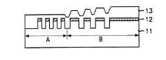
이하, 도1a 및 도1b를 참조하여 종래의 반도체 소자에서의 트렌치 소자분리막 형성 방법 및 그 문제점을 설명한다.Hereinafter, a method of forming a trench isolation layer and a problem thereof in a conventional semiconductor device will be described with reference to FIGS. 1A and 1B.
먼저, 도1a에 도시된 바와 같이, 실리콘 기판(11)상부에 패드 산화막(도시되지 않음), 산화방지막으로 질화막(12)을 형성한다. 그리고, 소자분리 마스크(도시되지 않음)를 사용한 상기 질화막(12), 패드산화막을 식각하고, 계속해서 식각제에 노출되는 실리콘 기판(11)을 소정 깊이 부분 식각하여 트렌치를 형성한다.First, as shown in FIG. 1A, a
이어서, 트렌치 내에 산화막(13)을 매립한다. 산화막(13)으로서 O3TEOS(Tetra ethyl orthosilicate)산화막 또는 HDP(High density plasma)산화막을 형성한다.Subsequently, an
한편, O3TEOS 산화막을 트렌치에 형성하는 경우 트렌치 내부로의 매립특성(gap-filling)은 우수하나 증착방법이 하부로부터 형성되는 것이 아니기 때문에 트렌치 내에 보이드 및 틈새를 형성시키는 문제점을 유발시킨다. 이러한 문제점을 극복하기 위하여 트렌치 내에 HDP를 사용하는 화학기상증착방법으로 산화막을 형성할 경우, 도1a와 같이 트렌치 내로의 매립특성이 우수하고 트렌치의 폭이 작은 구조물에서는 자체 평탄화 되는 특성이 있다. 즉, 트렌치 폭의 크기가 일정하지 않고 작고 좁은 간격을 갖는 트렌치 영역(A)과 트렌치 폭의 크기가 넓은 단일 면적을 갖는 트렌치 영역(B)이 공존할 경우 HDP방법의 자체 식각 작용에 의하여 작고 좁은 간격을 갖는 트렌치 영역(A) 위에서는 산화막(13)의 증착량이 감소하는 반면, 넓은 단일 면적을 갖는 트렌치 영역(B)의 상부에서는 설정한 양이 모두 증착 되어 산화막의 표면단차를 유발시킨다.On the other hand, when the O3 TEOS oxide film is formed in the trench, the gap filling in the trench is excellent, but since the deposition method is not formed from the bottom, it causes a problem of forming voids and gaps in the trench. In order to overcome this problem, when the oxide film is formed by a chemical vapor deposition method using HDP in the trench, as shown in FIG. 1A, the buried property into the trench is excellent and the structure having the small width of the trench has a self-flattening characteristic. That is, when the trench width A is not constant and the trench area A having a small and narrow gap and the trench area B having a single area having a wide trench width coexist, the small and narrow gap is caused by the self-etching action of the HDP method. While the deposition amount of the
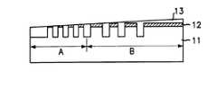
다음으로, 도1b에 도시된 바와 같이, 넓은 단일 면적을 갖는 트렌치 영역(B) 상부의 산화막(13) 두께를 화학적 기계적 연마 공정시 공정 타켓으로 설정하여 화학적 기계적 연마 공정을 진행할 경우, 작고 좁은 간격을 갖는 트렌치 영역(A)에서는 과도한 연마가 발생하게 된다.Next, as shown in Figure 1b, when the chemical mechanical polishing process is performed by setting the thickness of the
따라서, 경우에 따라 연마 정지 역할로 형성된 질화막(12)이 제거될 수 있고, 이에 따라 최종적으로 형성되는 트렌치형 소자분리막의 두께변화에 따라 동작특성이 부분적으로 달라지게 된다. 이러한 문제점을 극복하기 위한 트렌치 폭이 다양한 소자에서의 트렌치형 소자분리막 형성방법의 개발이 필요하게 되었다.Therefore, in some cases, the
전술한 바와 같은 문제점을 해결하기 위하여 안출된 본 발명은, 반도체 소자의 트렌치형 소자분리막의 형성시, 트렌치 폭의 크기의 차이에 의해 유도되는 추후 공정으로 증착되는 산화막의 표면단차를 줄일 수 있는 반도체 소자의 트렌치형 소자분리막 형성 방법 및 산화막 증착 방법을 제공하고자 함을 그 목적으로 한다.In order to solve the above problems, the present invention provides a semiconductor device capable of reducing the surface step of an oxide film deposited in a subsequent process induced by a difference in the size of a trench when forming a trench type device isolation film of a semiconductor device. An object of the present invention is to provide a trench type device isolation film formation method and an oxide film deposition method of a device.
상기와 같은 목적을 달성하기 위하여 본 발명의 반도체 소자의 트렌치형 소자분리막 형성 방법은, 트렌치 폭이 좁은 영역과 트렌치 폭이 넓은 영역이 혼재하는 반도체 소자의 트렌치형 소자분리막 형성 방법에 있어서, 기판 상부에 질화막을 형성한 후, 소자분리 마스크를 사용하여 상기 기판 상부에 트렌치를 형성하는 제1단계; 상기 트렌치 내부에 매립특성을 우수하게 하기 위하여 소정값의 제1 식각대 증착간의 비율을 갖는 HDP 방법으로 제1산화막을 상기 트렌치 내에 형성하는 제2단계; 상기 제2단계가 완료된 결과물 상부에 상기 제1 식각대 증착간의 비율에 대하여 상대적으로 낮은 제2 식각대 증착간의 비율을 갖는 HDP 방법으로 평탄화 특성이 우수한 제2산화막을 형성하는 제3단계; 및 상기 제2 및 제1산화막에 화학적 기계적 연마 공정을 실시하여 상기 질화막을 노출시키는 제4단계를 포함하여 이루어진다.In order to achieve the above object, a method of forming a trench type device isolation film of a semiconductor device of the present invention includes a method of forming a trench type device isolation film of a semiconductor device in which a narrow trench width and a wide trench width are mixed. Forming a trench in the upper portion of the substrate using a device isolation mask after forming a nitride film on the substrate; A second step of forming a first oxide film in the trench by an HDP method having a ratio between first etching and deposition of a predetermined value in order to improve buried characteristics in the trench; A third step of forming a second oxide film having excellent planarization characteristics by using an HDP method having a relatively low ratio between second etch deposits and a ratio between the first etch deposits and a ratio of deposition between the first etch deposits; And a fourth step of exposing the nitride film by performing a chemical mechanical polishing process on the second and first oxide films.
그리고, 본 발명의 HDP 화학기상증착방법의 산화막 형성 방법은, 갭필링 및 평탄화가 우수한 HDP화학기상증착방법의 산화막 증착 방법에 있어서, 소정 공정이 완료된 기판상에 매립특성을 우수하게 하기 위하여 소정값의 제1 식각대 증착간의 비율을 갖는 제1산화막을 형성하는 단계; 및 상기 제1산화막 상부에 상기 제1 식각대 증착간의 비율에 대하여 상대적으로 낮은 제2 식각대 증착간의 비율로 설정하여 평탄화 특성이 우수한 제2산화막을 형성하는 단계를 포함하여 이루어진다.In addition, the oxide film formation method of the HDP chemical vapor deposition method of the present invention, in the oxide film deposition method of the HDP chemical vapor deposition method excellent in gap filling and planarization, in order to improve the buried characteristics on the substrate on which the predetermined process is completed Forming a first oxide film having a ratio between first etch versus deposition of the first oxide film; And forming a second oxide film having excellent planarization characteristics by setting the ratio between the second etching stand deposition relatively low to the ratio between the first etching stand deposition on the first oxide film.
본 발명은, 사일렌, 아르곤, O2분위기의 산화막 증착 챔버 내에 HF(high frequency)를 인가하여 아르곤을 가속시켜 HF의 파워를 조절함으로써 식각/증착비가 조절된 산화막을 형성한다.The present invention forms an oxide film having an etch / deposition ratio controlled by applying HF (high frequency) in an oxide film deposition chamber in a xylene, argon, O2 atmosphere to accelerate argon to adjust the power of HF.
이하, 첨부된 도면을 참조하여 본 발명을 상세히 설명한다.Hereinafter, with reference to the accompanying drawings will be described in detail the present invention.
도2a 및 도2b는 본 발명의 일실시예에 따른 반도체 소자의 트렌치형 소자분리막 형성 방법을 나타내는 공정 단면도이다.2A and 2B are cross-sectional views illustrating a method of forming a trench type isolation layer in a semiconductor device according to an embodiment of the present invention.
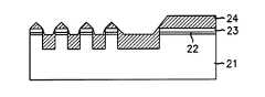
먼저, 도2a에 도시된 바와 같이, 실리콘 기판(21)상부에 50Å 내지 250Å의 두께를 갖는 패드 산화막(22), 500Å 내지 2500Å의 두께를 갖는 질화막(23)을 형성한다. 그리고, 소자분리 마스크(도시되지 않음)를 사용한 상기 질화막(23), 패드산화막(22)을 식각하고, 계속해서 식각제에 노출되는 실리콘 기판(21)을 소정 깊이 부분 식각하여 트렌치를 형성한다. 여기서 형성되는 트렌치의 깊이는 1500Å 내지 3500Å를 갖도록 한다. 이어서, 이러한 트렌치 측벽의 결함을 제거하기 위해 희생산화막(도시되지 않음)을 성장시키고 이것을 다시 습식식각하여 제거한다. 그리고, 전체구조 상부에 HDP 화학기상 증착 방법으로 식각/증착비를 10% 내지 40%로 설정하여 제1산화막(24)을 증착 하되, 형성되는 제1산화막(24)은 트렌치와 패드산화막(21)을 합친 두께 만큼으로 형성한다.First, as shown in FIG. 2A, a
다음으로, 도2b에 도시된 바와 같이, 상기 제1산화막(24)을 형성시킨 HDP화학기상 증착 챔버에서 인시츄(insitu) 방법으로 식각/증착비를 0에 가깝게 설정하여 제2산화막(25)을 형성한다. 이어서 이러한 제1 및 제2산화막(24, 25)의 밀도를 증가시키기 위해 열처리를 실시한다. 이러한 열처리는 900℃ 내지 1100℃의 질소분위기에서 30분 내지 1시간 동안 실시된다. 이어서, 제1 및 제2 산화막(24, 25)을 화학적 기계적 연마방법으로 연마하여 연마정지막인 질화막(23)을 노출시킨다. 본 발명에서 제시하는 화학적 기계적 연마 공정은, 산화막용 슬러리를 공급하여 이루어지며, 이때 연마압력은 7psi 내지 10psi, 연마 테이블 회전수는 30rpm 내지70rpm, 웨이퍼 회전수는 30rpm 내지 70rpm이 되도록 하여 설정하여 진행된다.Next, as shown in FIG. 2B, in the HDP chemical vapor deposition chamber in which the
전술한 바와 같이 진행되는 본 발명은, 제1 및 제2산화막의 형성후에 표면단차를 감소시켜 가격이 높고 불안정한 고선택비 슬러리를 사용하지 않고 기존의 산화막 슬러리로도 충분히 STI공정을 구현할 수 있어 고집적 디바이스를 위한 소자분리공정에 용이하게 사용될 수 있다.As described above, the present invention proceeds by reducing the surface step after the formation of the first and second oxide films, thereby enabling the STI process to be sufficiently implemented even with the existing oxide films slurry without using a high-cost and unstable high selectivity slurry. It can be easily used in the device isolation process for the device.
즉, 본 발명은 HDP화학기상증착방법으로 산화막을 증착할 때 식각/증착비(Etch/Deposition ratio)를 각각 다르게 조절하는 두 단계로 나누는 것을 그 특징으로 한다. 우선 매립 특성이 좋은 식각/증착비를 적용하여 매립특성을 만족시킨 후 두 번째 단계로 식각/증착비를 평탄화특성이 우수한 특성을 나타내도록 하여 플라즈마에 의한 식각이 전혀 없는 보통의 PE-CVD 저럼 증착한다.That is, the present invention is characterized by dividing into two stages of controlling the etching / deposition ratio differently when the oxide film is deposited by the HDP chemical vapor deposition method. First, by satisfying the landfill characteristics by applying the etch / deposition ratio with good landfill characteristics, the second step is to make the etch / deposition ratio exhibit the excellent flattening characteristics. do.
바람직하게, 본 발명은 트렌치형 소자분리막을 형성하는 방법의 적용이지만 본 발명의 사상은 여기서 국한되는 것이 아니고, 패턴의 밀도와 크기 차이가 심하고 HDP화학 기상 증착 방법의 산화막을 증착하는 모든 공정에 적용할 수 있다.Preferably, the present invention is an application of a method of forming a trench type isolation film, but the spirit of the present invention is not limited thereto, and the density and size of the pattern are severe and apply to all processes of depositing an oxide film of the HDP chemical vapor deposition method. can do.
이상에서 설명한 본 발명은 전술한 실시예 및 첨부된 도면에 의해 한정되는 것이 아니고, 본 발명이 기술적 사상을 벗어나지 않는 범위 내에서 여러 가지 치환, 변형 및 변경이 가능함이 본 발명이 속하는 기술분야에서 통상의 지식을 가진자에게 있어 명백할 것이다.The present invention described above is not limited to the above-described embodiment and the accompanying drawings, and various substitutions, modifications, and changes are possible within the scope of the present invention without departing from the technical idea. It will be evident to those who have knowledge of.
상기와 같이 이루어지는 본 발명은 트렌치형 소자분리막의 형성시 하나의 HDP-CVD 산화막 증착 장비 내에서 제1 및 제2산화막을 연속하여 증착하되, 제1산화막은 식각/증착비를 상대적으로 높게 설정하여 매립특성이 우수하게 하며, 제2산화막은 식각/증착비를 상대적으로 낮게 설정하여 평탄화 특성을 우수하게 함으로써, 트렌치 폭이 좁은 영역과 트렌치 폭이 넓은 영역과의 단차를 방지함으로써, 결과적으로 소자의 수율을 향상시킨다.In the present invention made as described above, the first and second oxide films are continuously deposited in one HDP-CVD oxide deposition apparatus during the formation of the trench type isolation layer, but the first oxide film is set to have a relatively high etching / deposition ratio. The buried property is excellent, and the second oxide film has a relatively low etching / deposition ratio to improve the planarization property, thereby preventing a step between a narrow trench width and a wide trench width. Improve yield.
도1a 및 도1b는 종래의 반도체 소자에서의 트렌치 소자분리막 형성 방법을 나타내는 공정 단면도.1A and 1B are cross-sectional views illustrating a method of forming a trench isolation layer in a conventional semiconductor device.
도2a 및 도2b는 본 발명의 일실시예에 따른 반도체 소자의 트렌치 소자분리막 형성 방법을 나타내는 공정 단면도.2A and 2B are cross-sectional views illustrating a method of forming a trench isolation layer in a semiconductor device in accordance with an embodiment of the present invention.
* 도면의 주요 부분에 대한 부호의 설명* Explanation of symbols for the main parts of the drawings
21 : 실리콘 기판 22 : 패드산화막21
23 : 질화막 24 : 제1열산화막23
25 : 제2열산화막25: second thermal oxide film
Claims (7)
Translated fromKoreanPriority Applications (1)
| Application Number | Priority Date | Filing Date | Title |
|---|---|---|---|
| KR1019970078027AKR100476372B1 (en) | 1997-12-30 | 1997-12-30 | Trench type isolation layer formation method for semiconductor devices with different trench widths |
Applications Claiming Priority (1)
| Application Number | Priority Date | Filing Date | Title |
|---|---|---|---|
| KR1019970078027AKR100476372B1 (en) | 1997-12-30 | 1997-12-30 | Trench type isolation layer formation method for semiconductor devices with different trench widths |
Publications (2)
| Publication Number | Publication Date |
|---|---|
| KR19990057948A KR19990057948A (en) | 1999-07-15 |
| KR100476372B1true KR100476372B1 (en) | 2005-07-07 |
Family
ID=37303392
Family Applications (1)
| Application Number | Title | Priority Date | Filing Date |
|---|---|---|---|
| KR1019970078027AExpired - Fee RelatedKR100476372B1 (en) | 1997-12-30 | 1997-12-30 | Trench type isolation layer formation method for semiconductor devices with different trench widths |
Country Status (1)
| Country | Link |
|---|---|
| KR (1) | KR100476372B1 (en) |
Families Citing this family (4)
| Publication number | Priority date | Publication date | Assignee | Title |
|---|---|---|---|---|
| KR100734254B1 (en)* | 2001-04-23 | 2007-07-02 | 삼성전자주식회사 | Wafer alignment key A method for separating semiconductor devices using trenches while maintaining signal sensitivity. |
| KR100478484B1 (en)* | 2002-10-09 | 2005-03-28 | 동부아남반도체 주식회사 | Formation method of trench in semiconductor device |
| KR100576424B1 (en)* | 2004-06-22 | 2006-05-08 | 동부일렉트로닉스 주식회사 | Trench Formation Method for Semiconductor Devices |
| KR100806793B1 (en)* | 2006-09-05 | 2008-02-27 | 동부일렉트로닉스 주식회사 | Manufacturing Method of Semiconductor Device |
Citations (10)
| Publication number | Priority date | Publication date | Assignee | Title |
|---|---|---|---|---|
| JPS6425433A (en)* | 1987-07-21 | 1989-01-27 | Matsushita Electric Industrial Co Ltd | Manufacture of semiconductor device |
| JPS6466939A (en)* | 1987-09-07 | 1989-03-13 | Fujitsu Ltd | Manufacture of semiconductor device |
| JPH05315441A (en)* | 1992-01-30 | 1993-11-26 | Sony Corp | Manufacture of semiconductor device provided with polishing process |
| JPH06334031A (en)* | 1993-05-25 | 1994-12-02 | Nec Corp | Element-isolation method for semiconductor device |
| KR960026585A (en)* | 1994-12-29 | 1996-07-22 | 김주용 | Method for manufacturing device isolation oxide film of semiconductor device |
| JPH0964166A (en)* | 1995-08-30 | 1997-03-07 | Toshiba Corp | Method for manufacturing semiconductor device |
| KR970053449A (en)* | 1995-12-27 | 1997-07-31 | 김주용 | Method for manufacturing device isolation region of semiconductor device |
| KR19980063317A (en)* | 1996-12-20 | 1998-10-07 | 윤종용 | Device Separation Method of Semiconductor Device |
| KR19980083839A (en)* | 1997-05-19 | 1998-12-05 | 윤종용 | Trench isolation method for semiconductor devices |
| KR100230431B1 (en)* | 1997-07-25 | 1999-11-15 | 윤종용 | Method of forming trench isolation using two kinds of oxides films |
- 1997
- 1997-12-30KRKR1019970078027Apatent/KR100476372B1/ennot_activeExpired - Fee Related
Patent Citations (11)
| Publication number | Priority date | Publication date | Assignee | Title |
|---|---|---|---|---|
| JPS6425433A (en)* | 1987-07-21 | 1989-01-27 | Matsushita Electric Industrial Co Ltd | Manufacture of semiconductor device |
| JPS6466939A (en)* | 1987-09-07 | 1989-03-13 | Fujitsu Ltd | Manufacture of semiconductor device |
| JPH05315441A (en)* | 1992-01-30 | 1993-11-26 | Sony Corp | Manufacture of semiconductor device provided with polishing process |
| JPH06334031A (en)* | 1993-05-25 | 1994-12-02 | Nec Corp | Element-isolation method for semiconductor device |
| KR960026585A (en)* | 1994-12-29 | 1996-07-22 | 김주용 | Method for manufacturing device isolation oxide film of semiconductor device |
| JPH0964166A (en)* | 1995-08-30 | 1997-03-07 | Toshiba Corp | Method for manufacturing semiconductor device |
| KR970053449A (en)* | 1995-12-27 | 1997-07-31 | 김주용 | Method for manufacturing device isolation region of semiconductor device |
| KR0172792B1 (en)* | 1995-12-27 | 1999-03-30 | 김주용 | Method of manufacturing isolation for semiconductor device |
| KR19980063317A (en)* | 1996-12-20 | 1998-10-07 | 윤종용 | Device Separation Method of Semiconductor Device |
| KR19980083839A (en)* | 1997-05-19 | 1998-12-05 | 윤종용 | Trench isolation method for semiconductor devices |
| KR100230431B1 (en)* | 1997-07-25 | 1999-11-15 | 윤종용 | Method of forming trench isolation using two kinds of oxides films |
Also Published As
| Publication number | Publication date |
|---|---|
| KR19990057948A (en) | 1999-07-15 |
Similar Documents
| Publication | Publication Date | Title |
|---|---|---|
| KR100898580B1 (en) | Device Separating Method of Semiconductor Device | |
| KR20010058498A (en) | Method of forming trench type isolation layer in semiconductor device | |
| KR20010064324A (en) | Method for forming isolation layer of semiconductor device using trench technology | |
| KR100476372B1 (en) | Trench type isolation layer formation method for semiconductor devices with different trench widths | |
| KR100895825B1 (en) | Device Separating Method of Semiconductor Device | |
| KR950009888B1 (en) | Manufacturing Method of Semiconductor Device | |
| KR100257764B1 (en) | Semiconductor device and manufacturing method | |
| KR100874429B1 (en) | Gap filling method in semiconductor device manufacturing | |
| KR100323868B1 (en) | Method of forming a trench type isolation film in a semiconductor device | |
| KR100511896B1 (en) | Method of manufacturing soi substrate | |
| KR100437541B1 (en) | Method for forming isolation layer of semiconductor device using two-step gap filling processes | |
| KR20080062560A (en) | Device Separating Method of Semiconductor Device | |
| KR20030050781A (en) | Method of forming a isolation film in flash memory device | |
| KR20010008560A (en) | Method For Forming The Isolation Layer Of Semiconductor Device | |
| KR100637095B1 (en) | Manufacturing method of semiconductor device | |
| KR20030059482A (en) | Method of forming isolating layer for semiconductor device | |
| KR100379524B1 (en) | Method for forming isolation layer in the semiconductor device | |
| KR20030050596A (en) | Method for forming isolation in semiconductor device | |
| KR100876874B1 (en) | Device Separating Method of Semiconductor Device | |
| KR100480625B1 (en) | Method for forming trench isolation and semiconductor device comprising the same | |
| KR20040005388A (en) | Method for forming isolation layer of semiconductor device | |
| KR20030051041A (en) | Method of forming a isolation film in flash memory device | |
| KR20020002603A (en) | Method for forming isolation in semiconductor device | |
| KR20040065030A (en) | Method for forming Shallow Trench Isolation in semiconductor device | |
| KR20020056659A (en) | Method for forming element isolating film of semicoductor device |
Legal Events
| Date | Code | Title | Description |
|---|---|---|---|
| PA0109 | Patent application | St.27 status event code:A-0-1-A10-A12-nap-PA0109 | |
| R17-X000 | Change to representative recorded | St.27 status event code:A-3-3-R10-R17-oth-X000 | |
| PG1501 | Laying open of application | St.27 status event code:A-1-1-Q10-Q12-nap-PG1501 | |
| R17-X000 | Change to representative recorded | St.27 status event code:A-3-3-R10-R17-oth-X000 | |
| PN2301 | Change of applicant | St.27 status event code:A-3-3-R10-R13-asn-PN2301 St.27 status event code:A-3-3-R10-R11-asn-PN2301 | |
| PN2301 | Change of applicant | St.27 status event code:A-3-3-R10-R13-asn-PN2301 St.27 status event code:A-3-3-R10-R11-asn-PN2301 | |
| A201 | Request for examination | ||
| PA0201 | Request for examination | St.27 status event code:A-1-2-D10-D11-exm-PA0201 | |
| D13-X000 | Search requested | St.27 status event code:A-1-2-D10-D13-srh-X000 | |
| D14-X000 | Search report completed | St.27 status event code:A-1-2-D10-D14-srh-X000 | |
| E902 | Notification of reason for refusal | ||
| PE0902 | Notice of grounds for rejection | St.27 status event code:A-1-2-D10-D21-exm-PE0902 | |
| P11-X000 | Amendment of application requested | St.27 status event code:A-2-2-P10-P11-nap-X000 | |
| P13-X000 | Application amended | St.27 status event code:A-2-2-P10-P13-nap-X000 | |
| E701 | Decision to grant or registration of patent right | ||
| PE0701 | Decision of registration | St.27 status event code:A-1-2-D10-D22-exm-PE0701 | |
| GRNT | Written decision to grant | ||
| PR0701 | Registration of establishment | St.27 status event code:A-2-4-F10-F11-exm-PR0701 | |
| PR1002 | Payment of registration fee | St.27 status event code:A-2-2-U10-U11-oth-PR1002 Fee payment year number:1 | |
| PG1601 | Publication of registration | St.27 status event code:A-4-4-Q10-Q13-nap-PG1601 | |
| PR1001 | Payment of annual fee | St.27 status event code:A-4-4-U10-U11-oth-PR1001 Fee payment year number:4 | |
| PR1001 | Payment of annual fee | St.27 status event code:A-4-4-U10-U11-oth-PR1001 Fee payment year number:5 | |
| PR1001 | Payment of annual fee | St.27 status event code:A-4-4-U10-U11-oth-PR1001 Fee payment year number:6 | |
| FPAY | Annual fee payment | Payment date:20110222 Year of fee payment:7 | |
| PR1001 | Payment of annual fee | St.27 status event code:A-4-4-U10-U11-oth-PR1001 Fee payment year number:7 | |
| LAPS | Lapse due to unpaid annual fee | ||
| PC1903 | Unpaid annual fee | St.27 status event code:A-4-4-U10-U13-oth-PC1903 Not in force date:20120304 Payment event data comment text:Termination Category : DEFAULT_OF_REGISTRATION_FEE | |
| PN2301 | Change of applicant | St.27 status event code:A-5-5-R10-R13-asn-PN2301 St.27 status event code:A-5-5-R10-R11-asn-PN2301 | |
| PN2301 | Change of applicant | St.27 status event code:A-5-5-R10-R13-asn-PN2301 St.27 status event code:A-5-5-R10-R11-asn-PN2301 | |
| PC1903 | Unpaid annual fee | St.27 status event code:N-4-6-H10-H13-oth-PC1903 Ip right cessation event data comment text:Termination Category : DEFAULT_OF_REGISTRATION_FEE Not in force date:20120304 | |
| PN2301 | Change of applicant | St.27 status event code:A-5-5-R10-R13-asn-PN2301 St.27 status event code:A-5-5-R10-R11-asn-PN2301 | |
| P22-X000 | Classification modified | St.27 status event code:A-4-4-P10-P22-nap-X000 |