KR100413649B1 - Method of manufacturing semiconductor devices - Google Patents
Method of manufacturing semiconductor devicesDownload PDFInfo
- Publication number
- KR100413649B1 KR100413649B1KR1019970001443AKR19970001443AKR100413649B1KR 100413649 B1KR100413649 B1KR 100413649B1KR 1019970001443 AKR1019970001443 AKR 1019970001443AKR 19970001443 AKR19970001443 AKR 19970001443AKR 100413649 B1KR100413649 B1KR 100413649B1
- Authority
- KR
- South Korea
- Prior art keywords
- film
- mask
- titanium
- etched
- forming
- Prior art date
- Legal status (The legal status is an assumption and is not a legal conclusion. Google has not performed a legal analysis and makes no representation as to the accuracy of the status listed.)
- Expired - Fee Related
Links
Images


Classifications
- H—ELECTRICITY
- H01—ELECTRIC ELEMENTS
- H01L—SEMICONDUCTOR DEVICES NOT COVERED BY CLASS H10
- H01L21/00—Processes or apparatus adapted for the manufacture or treatment of semiconductor or solid state devices or of parts thereof
- H01L21/02—Manufacture or treatment of semiconductor devices or of parts thereof
- H01L21/04—Manufacture or treatment of semiconductor devices or of parts thereof the devices having potential barriers, e.g. a PN junction, depletion layer or carrier concentration layer
- H01L21/18—Manufacture or treatment of semiconductor devices or of parts thereof the devices having potential barriers, e.g. a PN junction, depletion layer or carrier concentration layer the devices having semiconductor bodies comprising elements of Group IV of the Periodic Table or AIIIBV compounds with or without impurities, e.g. doping materials
- H01L21/30—Treatment of semiconductor bodies using processes or apparatus not provided for in groups H01L21/20 - H01L21/26
- H01L21/302—Treatment of semiconductor bodies using processes or apparatus not provided for in groups H01L21/20 - H01L21/26 to change their surface-physical characteristics or shape, e.g. etching, polishing, cutting
- H—ELECTRICITY
- H10—SEMICONDUCTOR DEVICES; ELECTRIC SOLID-STATE DEVICES NOT OTHERWISE PROVIDED FOR
- H10D—INORGANIC ELECTRIC SEMICONDUCTOR DEVICES
- H10D1/00—Resistors, capacitors or inductors
- H10D1/60—Capacitors
- H10D1/68—Capacitors having no potential barriers
- H10D1/682—Capacitors having no potential barriers having dielectrics comprising perovskite structures
- H—ELECTRICITY
- H01—ELECTRIC ELEMENTS
- H01L—SEMICONDUCTOR DEVICES NOT COVERED BY CLASS H10
- H01L21/00—Processes or apparatus adapted for the manufacture or treatment of semiconductor or solid state devices or of parts thereof
- H01L21/02—Manufacture or treatment of semiconductor devices or of parts thereof
- H01L21/04—Manufacture or treatment of semiconductor devices or of parts thereof the devices having potential barriers, e.g. a PN junction, depletion layer or carrier concentration layer
- H01L21/18—Manufacture or treatment of semiconductor devices or of parts thereof the devices having potential barriers, e.g. a PN junction, depletion layer or carrier concentration layer the devices having semiconductor bodies comprising elements of Group IV of the Periodic Table or AIIIBV compounds with or without impurities, e.g. doping materials
- H01L21/30—Treatment of semiconductor bodies using processes or apparatus not provided for in groups H01L21/20 - H01L21/26
- H01L21/31—Treatment of semiconductor bodies using processes or apparatus not provided for in groups H01L21/20 - H01L21/26 to form insulating layers thereon, e.g. for masking or by using photolithographic techniques; After treatment of these layers; Selection of materials for these layers
- H01L21/3105—After-treatment
- H01L21/311—Etching the insulating layers by chemical or physical means
- H01L21/31105—Etching inorganic layers
- H01L21/31111—Etching inorganic layers by chemical means
- H01L21/31116—Etching inorganic layers by chemical means by dry-etching
- H01L21/31122—Etching inorganic layers by chemical means by dry-etching of layers not containing Si, e.g. PZT, Al2O3
- H—ELECTRICITY
- H01—ELECTRIC ELEMENTS
- H01L—SEMICONDUCTOR DEVICES NOT COVERED BY CLASS H10
- H01L21/00—Processes or apparatus adapted for the manufacture or treatment of semiconductor or solid state devices or of parts thereof
- H01L21/02—Manufacture or treatment of semiconductor devices or of parts thereof
- H01L21/04—Manufacture or treatment of semiconductor devices or of parts thereof the devices having potential barriers, e.g. a PN junction, depletion layer or carrier concentration layer
- H01L21/18—Manufacture or treatment of semiconductor devices or of parts thereof the devices having potential barriers, e.g. a PN junction, depletion layer or carrier concentration layer the devices having semiconductor bodies comprising elements of Group IV of the Periodic Table or AIIIBV compounds with or without impurities, e.g. doping materials
- H01L21/30—Treatment of semiconductor bodies using processes or apparatus not provided for in groups H01L21/20 - H01L21/26
- H01L21/31—Treatment of semiconductor bodies using processes or apparatus not provided for in groups H01L21/20 - H01L21/26 to form insulating layers thereon, e.g. for masking or by using photolithographic techniques; After treatment of these layers; Selection of materials for these layers
- H01L21/3205—Deposition of non-insulating-, e.g. conductive- or resistive-, layers on insulating layers; After-treatment of these layers
- H01L21/321—After treatment
- H01L21/3213—Physical or chemical etching of the layers, e.g. to produce a patterned layer from a pre-deposited extensive layer
- H01L21/32133—Physical or chemical etching of the layers, e.g. to produce a patterned layer from a pre-deposited extensive layer by chemical means only
- H01L21/32135—Physical or chemical etching of the layers, e.g. to produce a patterned layer from a pre-deposited extensive layer by chemical means only by vapour etching only
- H01L21/32136—Physical or chemical etching of the layers, e.g. to produce a patterned layer from a pre-deposited extensive layer by chemical means only by vapour etching only using plasmas
Landscapes
- Engineering & Computer Science (AREA)
- Physics & Mathematics (AREA)
- Chemical & Material Sciences (AREA)
- Microelectronics & Electronic Packaging (AREA)
- Manufacturing & Machinery (AREA)
- Computer Hardware Design (AREA)
- General Physics & Mathematics (AREA)
- Power Engineering (AREA)
- Condensed Matter Physics & Semiconductors (AREA)
- Chemical Kinetics & Catalysis (AREA)
- General Chemical & Material Sciences (AREA)
- Inorganic Chemistry (AREA)
- Plasma & Fusion (AREA)
- Drying Of Semiconductors (AREA)
- Semiconductor Memories (AREA)
Abstract
Translated fromKoreanDescription
Translated fromKorean본 발명은 반도체 장치의 제조 방법에 관한 것으로, 특히 강유전체 재료, 고유전율 재료 및 백금의 에칭 방법에 관한 것이다.More particularly, the present invention relates to a ferroelectric material, a high dielectric constant material, and an etching method of platinum.
종래부터 반도체 기판 위에 형성된 강유전체막의 자발 분극(spontaneous polarization)을 이용한 비휘발성 메모리가 알려져 있다. 또, 고유전율 재료로 된 커패시터를 반도체 기판상에 구비한 DRAM(다이나믹 RAM)이 알려져 있다. 이러한 종류의 메모리 제조 공정에서는 강유전체 재료 및 고유전율 재료나 그들의 전극으로서 사용되는 백금(Pt)의 미세 가공이 필요하다.2. Description of the Related Art Nonvolatile memories using spontaneous polarization of a ferroelectric film formed on a semiconductor substrate are known. A DRAM (Dynamic RAM) having a capacitor made of a high dielectric constant material on a semiconductor substrate is known. In this type of memory fabrication process, micro-fabrication of ferroelectric materials and high-k materials and platinum (Pt) used as their electrodes is required.
포토레지스트를 마스크로 하고, 또 염소(Cl2) 가스의 플라즈마를 이용한 드라이 에칭법으로 강유전체 재료나 고유전율 재료를 가공하는 방법이 알려져 있다. 그러나, 강유전체 재료나 고유전율 재료는 녹는점(melting point)이 높고 비등점(boiling point)이 높은 금속의 복합 산화물이기 때문에 에칭 속도가 느리다There is known a method of processing a ferroelectric material or a high dielectric constant material by a dry etching method using a photoresist as a mask and a plasma of chlorine (Cl2 ) gas. However, since the ferroelectric material or the high-dielectric constant material is a complex oxide of a metal having a high melting point and a high boiling point, the etching rate is low
결국, 이 방법으로는 충분한 선택비를 얻기 곤란하기 때문에, 종래에는 포토레지스트 마스크를 불필요하게 두껍게 할 필요가 있었다. 따라서, 미세 가공이 곤란하였다.As a result, since it is difficult to obtain a sufficient selection ratio by this method, conventionally, it has been necessary to make the photoresist mask unnecessarily thick. Therefore, fine processing was difficult.
본 발명의 목적은 강유전체 재료, 고유전율 재료 및 백금의 미세 가공을 용이하게 실현할 수 있도록 하기 위한 것이다.An object of the present invention is to facilitate the microfabrication of a ferroelectric material, a high dielectric constant material and platinum.
도 1의 (a)∼(e)는 본 발명에 의한 반도체 장치의 제조 방법의 공정을 나타내는 단면도.1 (a) to 1 (e) are sectional views showing the steps of a method of manufacturing a semiconductor device according to the present invention.
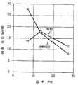
도 2는 염소와 산소의 혼합 가스의 플라즈마에 의한 드라이 에칭을 실시한 경우, 혼합 가스 중의 산소 가스의 체적 농도와, 백금, 강유전체 및 티탄의 각각의 에칭 속도와의 관계를 나타내는 도면.2 is a view showing the relationship between the volume concentration of oxygen gas in the mixed gas and the respective etching rates of platinum, ferroelectric, and titanium when dry etching is performed by plasma of a mixed gas of chlorine and oxygen.
도 3의 (a)∼(d)는 본 발명에 의한 반도체 장치의 제조 방법의 다른 공정을 나타내는 단면도.3 (a) to 3 (d) are cross-sectional views showing other steps of a method of manufacturing a semiconductor device according to the present invention.
도 4는 3염화붕소 가스의 플라즈마에 의한 드라이 에칭을 실시한 경우, 챔버 내의 압력과 티탄 및 산화 티탄의 각각의 에칭 속도와의 관계를 나타내는 도면.4 is a view showing the relationship between the pressure in the chamber and the respective etching rates of titanium and titanium oxide when dry etching is performed by plasma of boron trichloride gas.
5의 (a)∼(d)는 본 발명에 의한 반도체 장치의 제조 방법의 또 다른 공정을 나타내는 단면도.5 (a) to 5 (d) are cross-sectional views showing still another step of the method of manufacturing a semiconductor device according to the present invention.
< 도면의 주요 부분에 대한 부호의 설명 >Description of the Related Art
1, 11, 21 : 반도체 기판1, 11, 21: semiconductor substrate
2, 12, 22 : 디바이스 절연막2, 12, and 22: device insulating film
3, 13, 23 : 하층 백금막3, 13, 23: Lower platinum film
4, 14, 24 : 강유전체막4, 14, 24: ferroelectric film
5, 15, 25 : 상층 백금막5, 15, 25: upper layer platinum film
6, 17 : 티탄막6, 17: Thin film
7 : 포토레지스트 마스크7: Photoresist mask
16, 26 : 마스크 절연막16, 26: mask insulating film
상기 목적 달성을 위하여, 본 발명은 강유전체 재료, 고유전율 재료 및 백금 중 적어도 하나로 이루어지는 에칭 대상막 위에 산화하기 쉬운 금속막을 마스크로서 패턴 형성하고, 할로겐 가스와 산소 가스의 혼합 가스의 플라즈마로 에칭 대상막을 선택적으로 에칭하는 것이다. 이 방법에 의하면 마스크로서 형성된 금속막은 플라즈마에 의해 산화된다. 이 결과, 마스크의 에칭 속도는 느려지게 된다. 이것과는 대조적으로 에칭 대상막에 대해서는 빠른 에칭 속도가 확보된다. 따라서, 에칭의 높은 선택비가 실현되어 에칭 대상막의 미세 가공이 용이하게 된다.In order to achieve the above object, the present invention provides a method of manufacturing a semiconductor device, comprising the steps of forming a pattern on a film to be etched made of at least one of a ferroelectric material, a high-dielectric constant material and platinum, Thereby selectively etching. According to this method, a metal film formed as a mask is oxidized by plasma. As a result, the etching rate of the mask becomes slow. In contrast to this, a rapid etching rate is secured for the film to be etched. Therefore, a high selection ratio of etching is realized, and fine processing of the film to be etched is facilitated.
또, 본 발명에 의하면, 강유전체 재료 및 고유전율 재료 중 적어도 하나로 이루어지는 에칭 대상막 위에 절연물로 된 하층 마스크와 산화되기 쉬운 금속으로 된 상층 마스크를 패턴 형성하고, 할로겐 가스와 산소 가스의 혼합 가스의 플라즈마로 에칭 대상막을 선택적으로 에칭한 후에, 하층 마스크를 잔존시키면서 상층 마스크를 제거한다. 이 방법에 의하면, 상층 마스크로서 형성된 금속막은 플라즈마에 의해 산화된다. 이 결과, 마스크의 에칭 속도는 느려지게 된다. 이것과는 대조적으로, 에칭 대상막에 대해서는, 빠른 에칭 속도가 확보된다. 따라서, 에칭의 높은 선택비가 실현되고 에칭 대상막의 미세 가공이 용이하게 된다. 게다가, 상층 마스크를 제거할 때에는 에칭 대상막이 하층 마스크로 덮혀 있기 때문에, 그 에칭 대상막이 에칭 가스에 노출되지 않는다. 따라서, 강유전체 특성이나 고유전율 특성의 바람직하지 않은 변동이나 열화가 억제된다. 또한, 상층 마스크의 잔재 발생을 방지하기 위해서는 환원성을 갖는 가스의 플라즈마, 예를 들면 3염화붕소의 가스 플라즈마를 이용하여 상층 마스크를 에칭한다.According to the present invention, a lower layer mask made of an insulating material and an upper layer mask made of a metal that can be oxidized are pattern-formed on a film to be etched composed of at least one of a ferroelectric material and a high-dielectric constant material and a plasma of a mixed gas of halogen gas and oxygen gas After the etching target film is selectively etched, the upper layer mask is removed while remaining the lower layer mask. According to this method, the metal film formed as the upper layer mask is oxidized by the plasma. As a result, the etching rate of the mask becomes slow. In contrast to this, a high etching rate is secured for the film to be etched. Therefore, a high selection ratio of etching is realized and the microfabrication of the film to be etched is facilitated. Further, when removing the upper layer mask, the film to be etched is not exposed to the etching gas because the film to be etched is covered with the lower layer mask. Therefore, an undesirable fluctuation or deterioration of the ferroelectric characteristic or the high-dielectric constant characteristic is suppressed. Further, in order to prevent the remnants of the upper layer mask from being formed, the upper layer mask is etched using a plasma of a reducing gas, for example, a gas plasma of boron trichloride.
또, 본 발명에 의하면, 강유전체 재료 및 고유전율 재료 중 적어도 하나로 이루어진 에칭 대상막 위에 절연물을 마스크로서 패턴 형성하고, 가스 플라즈마로 에칭 대상막을 선택적으로 에칭한 후에, 절연물로 이루어진 마스크 중 상층 부분만을 제거한다. 이 방법에 의하면, 절연물로 이루어진 마스크를 이용한 드라이 에칭법의 채용에 의해 포토레지스트 마스크를 이용하는 경우에 비하여 에칭 대상막의 미세 가공이 용이하게 된다. 게다가, 마스크를 부분적으로 제거하였으므로, 이 마스크를 제거할 때에 에칭 대상막이 보호되는 결과, 강유전체 특성이나 고유전율 특성의 바람직하지 않은 변동 및 열화가 억제된다.Further, according to the present invention, after the pattern of the object to be etched, which is made of at least one of the ferroelectric material and the high-dielectric constant material, is pattern-formed by using the insulator as a mask and the etching target film is selectively etched by the gas plasma, do. According to this method, by employing the dry etching method using a mask made of an insulating material, fine processing of the film to be etched is easier than when a photoresist mask is used. In addition, since the mask is partially removed, the film to be etched is protected at the time of removing the mask, and as a result, undesirable fluctuation and deterioration of the ferroelectric characteristic and the high-dielectric constant characteristic are suppressed.
이하, 본 발명에 의한 반도체 장치의 제조 방법의 구체예에 대하여 도면을 참조하면서 설명한다.Hereinafter, specific examples of the method of manufacturing a semiconductor device according to the present invention will be described with reference to the drawings.
도 1의 (a)∼(e)는 본 발명에 의한 반도체 장치의 제조 방법의 공정을 나타내고 있다. 도 1의 (a)∼(e)에 있어서, 도면부호 1은 실리콘(Si) 단결정으로 이루어진 반도체 기판, 2는 산화 실리콘(SiO2)으로 이루어진 디바이스 절연막, 3은 하층백금(Pt)막, 4는 SBT, 즉 SrBi2Ta3O9로 이루어진 강유전체막, 5는 상층 백금(Pt)막, 6은 티탄(Ti)막, 7은 포토레지스트 마스크이다.1 (a) to 1 (e) show the steps of a method of manufacturing a semiconductor device according to the present invention. 1 (a) to 1 (e),
순서대로 설명하면, 반도체 기판(1)의 위에 디바이스 절연막(2)을 형성하고, 그 위에 하층 백금막(3), 강유전체막(4), 상층 백금막(5) 및 티탄막(6)을 차례로 형성하며, 다시 그 위에 포토리소그라피를 이용하여 원하는 패턴의 포토레지스트 마스크(7)를 형성한다(도 1의 (a)). 디바이스 절연막(2)은 CVD법에 의해, 하층 백금막(3), 상층 백금막(5) 및 티탄막(6)은 스퍼터링법에 의해, 그리고 강유전체막(4)은 졸겔법(sol-gel process)(상세하게는 스핀도포법, 미스트법 등)에 의해 각각 형성된다. 각각의 막 두께는, 예를 들면 디바이스 절연막(2)이 200 nm, 하층 백금막(3)이 300 nm, 강유전체막(4)이 200 nm, 상층 백금막(5)이 200 nm, 티탄막(6)이 200 nm, 포토레지스트 마스크(7)가 1200 nm 이다. 이 때, 티탄막(6)의 두께는 상층 백금막(5), 강유전체막(4) 및 하층 백금막(3)으로 이루어진 적층막의 두께의 합계의 1/10 이상으로 설정된다.The device insulating film 2 is formed on the
다음으로, 염소(Cl2) 가스의 플라즈마를 이용한 드라이 에칭법으로 티탄막(6)을 에칭하고(도 1의 (b)), 포토레지스트 마스크(7)를 산소(O2) 플라즈마에 의한 애싱(ashing) 처리로 제거한다(도 1의 (c)).Next, the chlorine (Cl2) ashing by a dry etching method using a plasma of a gas titanium film 6 is etched, and ((b) in Fig. 1), the photoresist mask 7 to the plasma of oxygen (O2) (as shown in Fig. 1 (c)).
그 다음으로, 패턴화된 티탄막(6)을 마스크로 하고, 또 염소(Cl2)와 산소(O2)의 혼합 가스의 플라즈마를 이용한 드라이 에칭법에 의해 상층 백금막(5),강유전체막(4) 및 하층 백금막(3)으로 이루어진 적층막을 에칭한다(도 1의 (d)). 이 때, 드라이 에칭을 위한 챔버를 이용하여, 예를 들면 염소 가스의 유량을 분당 12 cc(cc/분)로, 산소 가스의 유량을 분당 8 cc(cc/분)으로 각각 설정하고, 챔버내의 압력을 2 Pa로 유지하면서 또한 13.56 MHz의 고주파 전력을 5 W/cm2의 밀도로 인가함으로써 염소와 산소의 혼합가스의 플라즈마를 발생시킨다. 이 경우의 염소와 산소의 혼합 가스 중에서 산소 가스가 차지하는 체적 농도는 40 %이다.Next, the upper
또, 염소 가스의 플라즈마를 이용한 드라이 에칭법으로 티탄막(6)을 에칭함으로써, 이 티탄막(6)을 제거한다(도 1의 (e)). 이 때, 예를 들면 염소 가스의 유량을 분당 30 cc(cc/분)로 설정하고, 챔버내의 압력을 20 Pa로 유지하면서 13.56 MHz의 고주파전력을 0.7 W/cm2의 밀도로 인가함으로써, 염소 가스의 플라즈마를 발생시킨다. 이상의 공정에 의해, 반도체 기판(1) 위에 디바이스 절연막(2)을 개재하여 강유전체 커패시터가 형성된다. 그리고, 도 1의 (e)의 공정 후에 도시하지 않은 배선 공정이 실시된다.The titanium film 6 is removed by dry etching using a plasma of chlorine gas to remove the titanium film 6 (Fig. 1 (e)). At this time, for example, by setting the flow rate of chlorine gas to 30 cc (cc / min) per minute and applying a high frequency power of 13.56 MHz at a density of 0.7 W / cm2 while maintaining the pressure in the chamber at 20 Pa, Thereby generating a plasma of gas. By the above process, the ferroelectric capacitor is formed on the
도 2는 염소와 산소의 혼합 가스의 플라즈마에 의한 드라이 에칭을 실시한 경우, 이 혼합 가스 중의 산소 가스의 체적 농도와, 백금, 강유전체 및 티탄의 각각의 에칭 속도와의 관계를 나타내고 있다. 도 2에 있어서, 횡축은 염소와 산소의 혼합 가스 중에서 산소 가스가 차지하는 체적 농도를 나타내고, 종축은 백금, 강유전체 및 티탄 각각의 에칭 속도의 상대값을 나타내고 있다. 이 상대값은 산소 가스가 0 %(염소 가스는 100 %)인 경우 백금의 에칭 속도를 1로 한 것이다. 에칭을 위한 플라즈마는 챔버내의 압력을 2 Pa로 유지하면서 13.56 MHz의 고주파전력을 5 W/cm2의 밀도로 인가함으로써 생성하였다.Fig. 2 shows the relationship between the volume concentration of oxygen gas in the mixed gas and the respective etching rates of platinum, ferroelectric, and titanium when dry etching is performed by plasma of a mixed gas of chlorine and oxygen. In Fig. 2, the abscissa indicates the volume concentration occupied by the oxygen gas in the mixed gas of chlorine and oxygen, and the ordinate indicates the relative value of the etch rates of platinum, ferroelectric, and titanium, respectively. This relative value is obtained by setting the platinum etching rate to 1 when the oxygen gas is 0% (chlorine gas is 100%). Plasma for etching was generated by applying a high-frequency power of 13.56 MHz, while maintaining the pressure in the chamber to 2 Pa at a density of 5 W / cm2.
도 2에 의하면, 산소 가스의 체적 농도가 27 % 이상이 되면 티탄의 에칭 속도가 급격하게 감소한다. 이것은 티탄이 플라즈마에 의하여 산화되어 에칭되기 어렵게 된 것을 의미한다. 산소 가스의 체적 농도를 30 % 이상으로 설정하면, 티탄의 에칭 속도는 백금이나 강유전체 에칭 속도의 1/10 이하가 된다. 결국, 상기와 같이 티탄막(6)의 두께를 상층 백금막(5), 강유전체막(4) 및 하층 백금막(3)으로 이루어진 적층막 두께 합계의 1/10 이상으로 설정하면, 도 1의 (d)에 도시된 바와 같이, 패턴화된 티탄막(6)과 그 아래에 위치하는 적층막(3, 4, 5)의 필요한 부분을 남기면서, 이 적층막(3, 4, 5)의 불필요한 부분을 에칭으로 제거할 수 있다.According to Fig. 2, when the volume concentration of oxygen gas is 27% or more, the etching rate of titanium decreases sharply. This means that titanium is hardly oxidized and etched by the plasma. When the volume concentration of oxygen gas is set to 30% or more, the etching rate of titanium is 1/10 or less of the etching rate of platinum or ferroelectric. If the thickness of the titanium film 6 is set to 1/10 or more of the total thickness of the laminated film composed of the
이상과 같이 본 방법에 의하면, 백금과 강유전체의 적층막(3, 4, 5)의 위에 티탄막(6)을 마스크로서 패턴 형성하고, 염소와 산소의 혼합 가스의 플라즈마로 적층막(3, 4, 5)을 선택적으로 에칭하였으므로, 이 적층막(3, 4, 5)의 가공 정밀도가 향상된다. 또, 티탄막(6)의 패턴화를 위해서만 포토레지스트 마스크(7)를 이용하였으므로, 포토레지스트 마스크(7)의 두께를 저감할 수 있는 결과, 포토리소그라피의 해상도나 광학계의 초점심도 여유의 향상에 기여할 수 있다. 이들의 이점을 활용하면, 종래 가공성이 나쁘기 때문에 채용이 보류되었던 각종 강유전체 재료를 사용할 수 있게 되고, 반도체 장치의 특성이나 신뢰성, 수율을 향상시킬 수 있다.As described above, according to this method, the titanium film 6 is pattern-formed on the platinum and
디바이스 절연막(2)과 하층 백금막(3)의 사이에 접착층으로서 티탄층, 질화티탄층, 산화티탄층 중 어느 하나를 개재하여도 된다. 또, 상층 백금막(5)과 티탄막(6)의 사이에 상기 접착층을 개재하고, 티탄막(6)을 제거한 후에 남는 이 접착층을 상층 백금막(5)과 도 1의 (e)의 공정 후에 형성되는 산화 실리콘막과의 밀착성 확보에 이용하여도 된다.Any one of a titanium layer, a titanium nitride layer, and a titanium oxide layer may be interposed between the device insulating film 2 and the lower layer platinum film 3 as an adhesive layer. The adhesive layer remaining after removing the titanium film 6 with the adhesive layer interposed between the
또, 도 2로부터 알 수 있는 바와 같이, 상기 Pt와 SBT의 적층막에 한정되지 않고, Pt의 단층막이나, SBT의 단층막이어도 높은 선택비가 얻어진다. 졸겔법 또는 스퍼터링법에 의해 형성된 강유전체막의 일종인 PZT막, 즉 PbTiO3- PbZrO3막이나, 고유전율막의 일종인 BST막, 즉 BaTiO3- SrTiO3막의 에칭에 본 방법을 적용하는 것도 가능하다. 상기한 예에서는 마스크로서 티탄(Ti)막을 채용하였으나, 티탄 화합물 또는 티탄을 포함하는 합금으로 된 마스크를 채용하여도 된다. 또는, 크롬(Cr), 탄탈(Ta), 알루미늄(Al) 등의 산화되기 쉬운 다른 금속으로 된 마스크를 채용하여도 된다. 에칭 가스로서, Cl2와 O2의 혼합 가스 대신에 HBr, SF6, HC1 등의 다른 할로겐 가스와 O2의 혼합 가스를 선정하여도 된다. 다만, 백금(Pt)의 염화물은 그 불화물에 비하여 증기압이 높으므로, Pt의 에칭에는 불소계 가스보다도 염소계 가스가 바람직하다.Further, as can be seen from Fig. 2, not only the laminated film of Pt and SBT but also a single layer of Pt or a single layer of SBT has a high selectivity. A ferroelectric film one kinds formed by the sol-gel method or a sputtering method PZT film, that is, PbTiO3 - it is also possible to apply the SrTiO the method in thethird film etching - PbZrO3 film or a high dielectric constant film is a type of BST film, that is BaTiO3. In the above example, a titanium (Ti) film is used as a mask, but a mask made of an alloy containing a titanium compound or titanium may be employed. Alternatively, a mask made of another easily oxidizable metal such as chromium (Cr), tantalum (Ta), or aluminum (Al) may be employed. Instead of the mixed gas of Cl2 and O2 , another halogen gas such as HBr, SF6 , HCl, and a mixed gas of O2 may be selected as the etching gas. However, the chloride of platinum (Pt) has a higher vapor pressure than the fluoride, so chlorine gas is preferable to fluorine gas for etching of Pt.
그런데, 상기한 바와 같이, 강유전체 커패시터는 강유전체막을 상층 백금막과 하층 백금막과의 사이에 삽입한 구조를 가지고 있다. 반도체 장치의 사용시에 있어서 강유전체막의 측면에서의 표면층 리크(surface leakage)를 방지하기 위하여, 상층 백금막의 면적을 강유전체막의 면적보다 작게하는 것이 바람직하다. 이하, 상층 백금막과는 별도로 강유전체막과 하층 백금막을 에칭하는 방법에 대하여 설명한다.As described above, the ferroelectric capacitor has a structure in which a ferroelectric film is interposed between an upper platinum film and a lower platinum film. It is preferable to make the area of the upper platinum film smaller than the area of the ferroelectric film in order to prevent surface leakage of the side surface of the ferroelectric film at the time of using the semiconductor device. Hereinafter, a method of etching the ferroelectric film and the lower platinum film separately from the upper platinum film will be described.
도 3의 (a)∼(d)는 본 발명에 의한 반도체 장치의 제조 방법의 다른 공정을 나타내고 있다. 도 3의 (a)∼(d)에 있어서, 도면부호 11은 실리콘(Si) 단결정으로 된 반도체 기판, 12는 산화 실리콘(SiO2)으로 된 디바이스 절연막, 13은 하층 백금(Pt)막, 14는 SBT, 즉 SrBi2Ta3O9로 된 강유전체막, 15는 상층 백금(Pt)막, 16은 산화 실리콘의 일종인 NSG (non-doped silicate glass)로 된 마스크 절연막, 17은 티탄(Ti)막이다.3 (a) to 3 (d) show other steps of the method for manufacturing a semiconductor device according to the present invention. (Si) single
순서대로 설명하면, 반도체 기판(11)의 위에 디바이스 절연막(12)을 형성하고, 그 위에 하층 백금막(13), 강유전체막(14) 및 상층 백금막(15)을 차례로 형성한 후, 상층 백금막(15)을 원하는 패턴으로 에칭한다(도 3의 (a)). 디바이스 절연막(12)은 CVD법에 의해, 하층 백금막(13) 및 상층 백금막(15)은 스퍼터링법에 의해, 강유전체막(14)은 졸겔법(상세하게는 스핀도포법, 미스트법 등)에 의해 각각 형성된다. 각각의 막 두께는, 예를 들면 디바이스 절연막(12)이 100 nm, 하층 백금막(13)이 200 nm, 강유전체막(14)이 200 nm, 상층 백금막(15)이 200 nm이다. 여기에서는 상층 백금막(15)만을 에칭하므로 그 에칭에는 포토레지스트 마스크를 이용한 드라이 에칭법을 적용할 수 있다. 에칭 가스는, 예를 들면 염소(Cl2) 가스이다. 포토레지스트 마스크는 산소(O2) 플라즈마에 의한 애싱 처리로 제거된다.The
다음으로, 패턴화된 상층 백금막(15)을 덮도록 마스크 절연막(16)을 CVD법에의해 형성하고, 그 위에 티탄막(17)을 스퍼터링법에 의해 형성한 후, 티탄막(17) 및 마스크 절연막(16)을 상층 백금막(15)보다 큰 패턴으로 에칭한다(도 3의 (b)). 각각의 막두께는, 예를 들면 마스크 절연막(16)이 100 nm, 티탄막(17)이 200 nm이다. 이 에칭에도 포토레지스트 마스크를 이용한 드라이 에칭법을 적용할 수 있다. 에칭 가스는, 예를 들면 티탄막(17)에 대해서는 Cl2가스를, 마스크 절연막(16)에 대해서는 CF4가스를 사용한다. 포토레지스트 마스크는 산소(O2) 플라즈마에 의한 애싱 처리로 제거된다.Next, a
계속하여, 패턴화된 티탄막(17) 및 절연막(16)을 마스크로 하면서 염소(Cl2)와 산소(O2)의 혼합 가스의 플라즈마를 이용한 드라이 에칭법에 의해 강유전체막(14)을 에칭한다(도 3의 (c)). 이 때, 티탄막(17)은 부분적으로 산화 티탄(TiO2)으로 변화한다.Subsequently, the
또, 환원성을 갖는 3염화붕소(BCl3) 가스의 플라즈마를 이용한 드라이 에칭법으로 티탄막(17)을 에칭함으로써 절연막(16)을 남기면서 티탄막(17)을 제거한다(도 3의 (d)). 이 때, 예를 들면 3염화붕소 가스의 유량을 분당 80 cc(cc/분)로 설정하고, 챔버내의 압력을 13.3 Pa(= 100 mTorr)로 유지하면서 115 W의 고주파 전력을 인가함으로써 3염화붕소 가스의 플라즈마를 발생시킨다. 그리고, 도 3의 (d)의 공정 후에, 절연막(16)의 천공을 포함하는 도시하지 않은 배선 공정이 실시된다.The
상술한 바와 같이, 본 방법에 의하면, 강유전체막(14)의 위에 티탄막(17)을마스크로서 패턴 형성하고, 염소와 산소의 혼합 가스의 플라즈마로 강유전체막(14)을 선택적으로 에칭하였으므로, 이 강유전체막(14)의 가공 정밀도가 향상한다. 게다가, 마스크로서 사용된 티탄막(17)은 완전하게 제거될 수 있다.As described above, according to the present method, since the
도 4는 3염화붕소 가스의 플라즈마에 의한 드라이 에칭을 실시한 경우, 챔버 내의 압력과 티탄 및 산화티탄 각각의 에칭 속도의 관계를 도시하고 있다. 압력이 13.3 Pa일 때에 티탄과 산화티탄의 에칭 속도가 거의 같아지는 것을 알 수 있다. 결국, 상기 조건에서 티탄막(17)을 에칭하면 티탄 및 산화티탄의 잔재가 발생하지 않는다. 따라서, 배선 공정에 지장을 주는 일은 없다. 게다가, 티탄막(17)을 제거할 때 강유전체막(14)이 마스크 절연막(16)으로 덮혀 있으므로, 이 강유전체막(14)이 에칭 가스에 노출되지 않는다. 따라서, 강유전체 특성의 바람직하지 않은 변동이나 열화가 억제된다. 실험에 의하면, 강유전체막(14)의 잔류분극으로서 15μC/cm2가, 그 내압으로서 30 V가 각각 얻어졌다. 디바이스 절연막(12)과 하층 백금막(13)과의 사이 및 상층 백금막(15)과 마스크 절연막(16)의 사이에 각각 접착층으로서 티탄층, 질화티탄층, 산화티탄층 중 어느 하나를 개재하여도 된다.Fig. 4 shows the relationship between the pressure in the chamber and the etching rate of titanium and titanium oxide, respectively, when dry etching is performed by plasma of boron trichloride gas. It can be seen that the etching rates of titanium and titanium oxide are almost equal when the pressure is 13.3 Pa. As a result, when the
또, 강유전체막의 일종인 PZT막이나, 고유전율막의 일종인 BST막의 에칭에 본 방법을 적용하는 것도 가능하다. 마스크 절연막(16)은 질화실리콘(Si3N4)막이어도 된다. 다만, 질화 실리콘의 성막(成膜)시에 암모니아(NH3) 가스 등의 수소를 포함하는 가스를 이용하면 강유전체막(14)에 열화가 생기므로 성막 방법의 선정이 중요하다. 티탄막(17)을 대신하여 티탄 화합물 또는 티탄을 포함하는 합금으로 된 마스크를 채용하여도 된다. 또는, 크롬(Cr), 탄탈(Ta), 알루미늄(Al) 등의 산화되기 쉬운 다른 금속으로 된 마스크를 채용하여도 된다. 티탄막(17)의 에칭 가스로서, Cl2, CHCl3, HCl 등의 염소계 가스를 사용하여도 된다. 다만, 잔재의 발생방지의 관점에서 3염화붕소(BCl3) 가스가 가장 적합하다. 상층 백금막(15)을 에칭할 때에도 NSG와 티탄의 적층막을 마스크로한 드라이 에칭법이 적용 가능하다. 티탄막 또는 NSG막만을 마스크로 하여 상층 백금막(15)을 에칭하여도 된다. 다만, 선택비는 티탄, NSG, 포토레지스트의 순서로 낮아진다. 결국, 단층 마스크를 사용하는 경우에는 티탄막으로 된 마스크를 채용함으로써, 이 중에서는 최대의 선택비가 얻어진다. 또, 강유전체막(14)과 하층 백금막(13)을 동시에 에칭하여도 된다.It is also possible to apply this method to the etching of a PZT film, which is one type of ferroelectric film, or a BST film, which is a type of high-permittivity film. The
도 5의 (a)∼(d)는 본 발명에 의한 반도체 장치의 제조 방법의 또 다른 공정을 도시하고 있다. 도 5의 (a)∼(d)에 있어서, 도면부호 21은 실리콘(Si) 단결정으로 된 반도체 기판, 22는 산화 실리콘(SiO2)으로 된 디바이스 절연막, 23은 하층 백금(Pt)막, 24는 SBT, 즉 SrBi2Ta3O9로 이루어진 강유전체막, 25는 상층 백금(Pt)막, 26은 NSG로 이루어진 마스크 절연막이다.5 (a) to 5 (d) show still another step of the method of manufacturing a semiconductor device according to the present invention. 5,
순서대로 설명하면, 반도체 기판(21) 위에 디바이스 절연막(22)을 형성하고, 그 위에 하층 백금막(23), 강유전체막(24) 및 상층 백금막(25)을 순차로 형성한 후, 상층 백금막(25)을 원하는 패턴으로 에칭한다(도 5의 (a)). 이 공정은 도 3의 (a)의 공정과 같다.The
다음에, 패턴화된 상층 백금막(25)을 덮도록 마스크 절연막(26)을 CVD법에의해 형성한 후, 이 마스크 절연막(26)을 상층 백금막(25)보다 큰 패턴으로 에칭한다(도 5의 (b)). 마스크 절연막(26)의 두께는, 예를 들면 500 nm이다. 이 에칭에는 포토레지스트 마스크를 이용한 드라이 에칭법을 적용할 수 있다. 에칭 가스는, 예를 들면 CF4, CHF3등의 붕소계 가스이다. 포토레지스트 마스크는 산소(O2) 플라즈마에 의한 애싱 처리로 제거된다.Next, after the
계속하여, 패턴화된 절연막(26)을 마스크로 하고, 또 염소(Cl2)와 산소(O2)의 혼합 가스의 플라즈마를 이용한 드라이 에칭법에 의해 강유전체막(24)을 에칭한다(도 5의 (c)).Subsequently, the
또, CF4, CHF3등의 붕소계 가스의 플라즈마를 이용한 드라이 에칭법으로 마스크 절연막(26)을 에칭함으로써, 이 마스크 절연막(26)을 일부 제거한다(도5의 (d)). 이 때, 예를 들면 마스크 절연막(26)의 두께가 100 nm가 되도록 에칭 시간을 조정한다. 그리고, 도 5의 (d)의 공정 후에 절연막(26)의 천공을 포함하는 도시하지 않은 배선 공정이 실시된다.The
본 방법에 의하면, NSG로 된 마스크 절연막(26)을 이용한 드라이 에칭법의 채용에 의해 강유전체막(24)의 미세 가공이 용이해진다. 게다가, 도 5의 (d)의 공정에 있어서 강유전체막(24)이 마스크 절연막(26)으로 덮혀 있으므로, 이 강유전체막(24)이 에칭 가스에 노출되지 않는다. 따라서, 강유전체 특성의 바람직하지 않은 변동이나 열화가 억제된다. 실험에 의하면, 강유전체막(24)의 잔류분극으로서 13∼15 μC/cm2가, 그 내압으로서 25∼30 V가 각각 얻어졌다. 디바이스 절연막(22)과 하층 백금막(23)의 사이 및 상층 백금막(25)과 마스크 절연막(26)의 사이에 각각 접착층으로서 티탄층, 질화티탄층, 산화티탄층 중 어느 하나를 개재하여도 된다.According to this method, the fine processing of the
또, 강유전체막의 일종인 PZT막이나 고유전율막의 일종인 BST막의 에칭에 본 방법을 적용하는 것도 가능하다. 마스크 절연막(26)은 질화 실리콘(Si3N4)막이어도 된다. 또, 강유전체막(24)과 하층 백금막(23)을 동시에 에칭하여도 된다.It is also possible to apply this method to the etching of a PZT film, which is one type of ferroelectric film, or a BST film, which is a type of high-permittivity film. The
상술한 본 발명에 의하면, 마스크로서 형성된 금속막은 플라즈마에 의하여 산화된다. 그 결과, 마스크의 에칭 속도는 느려진다. 이것과는 대조적으로, 에칭 대상막에 대해서는 빠른 에칭 속도가 확보된다. 따라서, 에칭의 높은 선택비가 실현되고, 에칭 대상막의 미세 가공이 용이해지는 효과를 얻을 수있다.According to the present invention described above, the metal film formed as a mask is oxidized by plasma. As a result, the etching rate of the mask becomes slow. In contrast to this, a high etching rate is secured for the film to be etched. Therefore, a high selection ratio of etching can be realized, and an effect of facilitating the fine processing of the film to be etched can be obtained.
또한, 상층 마스크로서 형성된 금속막은 플라즈마에 의하여 산화된다. 그 결과, 마스크의 에칭 속도는 느려진다. 이것과는 대조적으로, 에칭 대상막에 대해서는 빠른 에칭 속도가 확보된다. 따라서, 에칭의 높은 선택비가 실현되고, 에칭 대상막의 미세 가공이 용이해진다. 게다가, 상층 마스크를 제거할 때에는 에칭 대상막이 하층 마스크로 덮혀 있으므로, 이 에칭 대상막이 에칭가스에 노출되지 않는다. 따라서, 강유전체 특성이나 고유전율 특성의 바람직하지 않은 변동이나 열화가 억제되는 효과를 얻을 수 있다.Further, the metal film formed as the upper layer mask is oxidized by plasma. As a result, the etching rate of the mask becomes slow. In contrast to this, a high etching rate is secured for the film to be etched. Therefore, a high selection ratio of etching is realized, and fine processing of the film to be etched is facilitated. In addition, when the upper layer mask is removed, the film to be etched is covered with the lower layer mask, so that the film to be etched is not exposed to the etching gas. Therefore, it is possible to obtain an effect of suppressing undesirable fluctuation and deterioration of the ferroelectric characteristic and the high-dielectric constant characteristic.
또한, 절연물로 이루어진 마스크를 이용한 드라이 에칭법의 채용에 의해 포토레지스트 마스크를 이용하는 경우에 비하여 에칭 대상막의 미세 가공이 용이해진다. 게다가, 마스크를 부분적으로 제거하였으므로, 이 마스크를 제거할 때에 에칭 대상막이 보호되는 결과, 강유전체 특성이나 고유전율 특성의 바람직하지 않은 변동이나 열화가 억제되는 효과를 얻을 수 있다.Further, by employing a dry etching method using a mask made of an insulating material, fine processing of the film to be etched is easier than when a photoresist mask is used. In addition, since the mask is partially removed, the film to be etched is protected at the time of removing the mask. As a result, it is possible to obtain an effect of suppressing undesirable fluctuation and deterioration of the ferroelectric characteristic and the high-dielectric constant characteristic.
본 발명의 바람직한 실시예들은 예시의 목적을 위해 개시된 것이며, 당업자라면 첨부된 특허 청구 범위에 개시된 본 발명의 사상과 범위를 통해 각종 수정, 변경, 대체 및 부가가 가능할 것이다.While the present invention has been particularly shown and described with reference to exemplary embodiments thereof, it is evident that many alternatives, modifications, and variations will be apparent to those skilled in the art.
Claims (12)
Translated fromKoreanApplications Claiming Priority (3)
| Application Number | Priority Date | Filing Date | Title |
|---|---|---|---|
| JP96-011,481 | 1996-01-26 | ||
| JP1148196 | 1996-01-26 | ||
| JP96-011481 | 1996-01-26 |
Publications (2)
| Publication Number | Publication Date |
|---|---|
| KR970060400A KR970060400A (en) | 1997-08-12 |
| KR100413649B1true KR100413649B1 (en) | 2004-04-28 |
Family
ID=11779253
Family Applications (1)
| Application Number | Title | Priority Date | Filing Date |
|---|---|---|---|
| KR1019970001443AExpired - Fee RelatedKR100413649B1 (en) | 1996-01-26 | 1997-01-20 | Method of manufacturing semiconductor devices |
Country Status (5)
| Country | Link |
|---|---|
| US (1) | US5840200A (en) |
| EP (1) | EP0786805A2 (en) |
| KR (1) | KR100413649B1 (en) |
| CN (1) | CN1129958C (en) |
| TW (1) | TW382139B (en) |
Families Citing this family (55)
| Publication number | Priority date | Publication date | Assignee | Title |
|---|---|---|---|---|
| US5930639A (en)* | 1996-04-08 | 1999-07-27 | Micron Technology, Inc. | Method for precision etching of platinum electrodes |
| US5997642A (en)* | 1996-05-21 | 1999-12-07 | Symetrix Corporation | Method and apparatus for misted deposition of integrated circuit quality thin films |
| JPH1098162A (en)* | 1996-09-20 | 1998-04-14 | Hitachi Ltd | Method for manufacturing semiconductor integrated circuit device |
| TW365691B (en)* | 1997-02-05 | 1999-08-01 | Samsung Electronics Co Ltd | Method for etching Pt film of semiconductor device |
| EP0865079A3 (en)* | 1997-03-13 | 1999-10-20 | Applied Materials, Inc. | A method for removing redeposited veils from etched platinum surfaces |
| US6083841A (en)* | 1997-05-15 | 2000-07-04 | Rohm Co., Ltd. | Method of etching gallium-nitride based compound semiconductor layer and method of manufacturing semiconductor light emitting device utilizing the same |
| DE19728472A1 (en)* | 1997-07-03 | 1999-01-07 | Siemens Ag | Structuring process |
| EP0895278A3 (en)* | 1997-08-01 | 2000-08-23 | Siemens Aktiengesellschaft | Patterning process |
| EP0907203A3 (en)* | 1997-09-03 | 2000-07-12 | Siemens Aktiengesellschaft | Patterning method |
| KR100252047B1 (en)* | 1997-11-13 | 2000-04-15 | 윤종용 | Method for etching a metal layer using a hard mask |
| KR100252889B1 (en)* | 1997-11-14 | 2000-04-15 | 김영환 | Platinum Etching Method |
| US6265318B1 (en) | 1998-01-13 | 2001-07-24 | Applied Materials, Inc. | Iridium etchant methods for anisotropic profile |
| US6323132B1 (en) | 1998-01-13 | 2001-11-27 | Applied Materials, Inc. | Etching methods for anisotropic platinum profile |
| US6919168B2 (en) | 1998-01-13 | 2005-07-19 | Applied Materials, Inc. | Masking methods and etching sequences for patterning electrodes of high density RAM capacitors |
| EP1048064A1 (en)* | 1998-01-13 | 2000-11-02 | Applied Materials, Inc. | Etching methods for anisotropic platinum profile |
| KR100269323B1 (en)* | 1998-01-16 | 2000-10-16 | 윤종용 | Method for etching platinum layer in semiconductor device |
| US6287975B1 (en)* | 1998-01-20 | 2001-09-11 | Tegal Corporation | Method for using a hard mask for critical dimension growth containment |
| JP3698885B2 (en)* | 1998-02-18 | 2005-09-21 | 富士通株式会社 | Method for manufacturing device using ferroelectric film |
| US6277760B1 (en)* | 1998-06-26 | 2001-08-21 | Lg Electronics Inc. | Method for fabricating ferroelectric capacitor |
| EP1001459B1 (en)* | 1998-09-09 | 2011-11-09 | Texas Instruments Incorporated | Integrated circuit comprising a capacitor and method |
| KR100318457B1 (en)* | 1998-10-28 | 2002-02-19 | 박종섭 | A method for forming ferroelectric film using plasma |
| JP2000200779A (en)* | 1998-10-30 | 2000-07-18 | Toshiba Corp | Etching method, chemical vapor deposition apparatus, cleaning method for chemical vapor deposition apparatus, and quartz member for chemical vapor deposition apparatus |
| US6204158B1 (en)* | 1998-12-18 | 2001-03-20 | Advanced Technology Materials, Inc. | Reduced diffusion of a mobile specie from a metal oxide ceramic into the substrate |
| EP1014399B1 (en)* | 1998-12-22 | 2006-05-17 | Matsushita Electric Industrial Co., Ltd. | Flexible thin film capacitor and method for producing the same |
| US6349456B1 (en)* | 1998-12-31 | 2002-02-26 | Motorola, Inc. | Method of manufacturing photodefined integral capacitor with self-aligned dielectric and electrodes |
| US6406818B1 (en)* | 1999-03-31 | 2002-06-18 | Photronics, Inc. | Method of manufacturing photomasks by plasma etching with resist stripped |
| JP3415487B2 (en)* | 1999-06-14 | 2003-06-09 | Necエレクトロニクス株式会社 | Method for manufacturing semiconductor device |
| US6306312B1 (en)* | 1999-06-30 | 2001-10-23 | Lam Research Corporation | Method for etching a gold metal layer using a titanium hardmask |
| US6358857B1 (en) | 1999-07-23 | 2002-03-19 | Micron Technology, Inc. | Methods of etching insulative materials, of forming electrical devices, and of forming capacitors |
| DE19935131B4 (en)* | 1999-07-27 | 2006-01-26 | Infineon Technologies Ag | Method for eliminating redepositions from a wafer |
| US6436838B1 (en) | 2000-04-21 | 2002-08-20 | Applied Materials, Inc. | Method of patterning lead zirconium titanate and barium strontium titanate |
| JP4605554B2 (en)* | 2000-07-25 | 2011-01-05 | 独立行政法人物質・材料研究機構 | Mask material for dry etching |
| JP5013494B2 (en)* | 2001-04-06 | 2012-08-29 | ルネサスエレクトロニクス株式会社 | Manufacturing method of magnetic memory |
| JP2003059905A (en)* | 2001-07-31 | 2003-02-28 | Applied Materials Inc | Etching method, method of manufacturing capacitor, and semiconductor device |
| JP4865978B2 (en) | 2002-02-28 | 2012-02-01 | 富士通セミコンダクター株式会社 | Manufacturing method of semiconductor device |
| JP2003257942A (en)* | 2002-02-28 | 2003-09-12 | Fujitsu Ltd | Method for manufacturing semiconductor device |
| JP4014902B2 (en)* | 2002-03-15 | 2007-11-28 | 富士通株式会社 | Manufacturing method of semiconductor device |
| US20040007561A1 (en)* | 2002-07-12 | 2004-01-15 | Applied Materials, Inc. | Method for plasma etching of high-K dielectric materials |
| DE10260352A1 (en)* | 2002-12-20 | 2004-07-15 | Infineon Technologies Ag | Method of manufacturing a capacitor arrangement and capacitor arrangement |
| US6897501B2 (en)* | 2003-02-28 | 2005-05-24 | Infineon Technologies Aktiengesellschaft | Avoiding shorting in capacitors |
| US7230292B2 (en)* | 2003-08-05 | 2007-06-12 | Micron Technology, Inc. | Stud electrode and process for making same |
| US20060102197A1 (en)* | 2004-11-16 | 2006-05-18 | Kang-Lie Chiang | Post-etch treatment to remove residues |
| US7375038B2 (en)* | 2005-09-28 | 2008-05-20 | Applied Materials, Inc. | Method for plasma etching a chromium layer through a carbon hard mask suitable for photomask fabrication |
| US7846845B2 (en)* | 2006-10-26 | 2010-12-07 | Applied Materials, Inc. | Integrated method for removal of halogen residues from etched substrates in a processing system |
| US7655571B2 (en)* | 2006-10-26 | 2010-02-02 | Applied Materials, Inc. | Integrated method and apparatus for efficient removal of halogen residues from etched substrates |
| US7946759B2 (en)* | 2007-02-16 | 2011-05-24 | Applied Materials, Inc. | Substrate temperature measurement by infrared transmission |
| WO2012148568A1 (en) | 2011-03-01 | 2012-11-01 | Applied Materials, Inc. | Method and apparatus for substrate transfer and radical confinement |
| US11171008B2 (en) | 2011-03-01 | 2021-11-09 | Applied Materials, Inc. | Abatement and strip process chamber in a dual load lock configuration |
| US8992689B2 (en) | 2011-03-01 | 2015-03-31 | Applied Materials, Inc. | Method for removing halogen-containing residues from substrate |
| US10453694B2 (en) | 2011-03-01 | 2019-10-22 | Applied Materials, Inc. | Abatement and strip process chamber in a dual loadlock configuration |
| US8845816B2 (en) | 2011-03-01 | 2014-09-30 | Applied Materials, Inc. | Method extending the service interval of a gas distribution plate |
| JP5766027B2 (en)* | 2011-05-20 | 2015-08-19 | 富士フイルム株式会社 | Dry etching method and device manufacturing method |
| JP6545460B2 (en) | 2012-02-29 | 2019-07-17 | アプライド マテリアルズ インコーポレイテッドApplied Materials,Incorporated | Abatement and stripping process chamber in load lock configuration |
| US8796044B2 (en)* | 2012-09-27 | 2014-08-05 | International Business Machines Corporation | Ferroelectric random access memory with optimized hardmask |
| CN117238763B (en)* | 2023-08-30 | 2024-09-24 | 上海稷以科技有限公司 | Silicon dioxide etching method based on titanium substrate |
Family Cites Families (13)
| Publication number | Priority date | Publication date | Assignee | Title |
|---|---|---|---|---|
| US3836446A (en)* | 1971-05-10 | 1974-09-17 | Raytheon Co | Semiconductor devices manufacture |
| US3975252A (en)* | 1975-03-14 | 1976-08-17 | Bell Telephone Laboratories, Incorporated | High-resolution sputter etching |
| JPS60247816A (en)* | 1984-05-24 | 1985-12-07 | Mitsubishi Electric Corp | Production of thin film magnetic head |
| JPS61248048A (en)* | 1985-04-26 | 1986-11-05 | Toshiba Corp | Mask for transferring pattern |
| JPS6292323A (en)* | 1985-10-17 | 1987-04-27 | Nec Corp | Dry etching method |
| JPS62120019A (en)* | 1985-11-20 | 1987-06-01 | Fujitsu Ltd | Manufacturing method of semiconductor device |
| JPH0589662A (en)* | 1991-09-25 | 1993-04-09 | Seiko Epson Corp | Manufacture of semiconductor device |
| US5254217A (en)* | 1992-07-27 | 1993-10-19 | Motorola, Inc. | Method for fabricating a semiconductor device having a conductive metal oxide |
| JP2972506B2 (en)* | 1993-11-02 | 1999-11-08 | 日本電気株式会社 | Method for etching alloy containing Pt as main component |
| US5443688A (en)* | 1993-12-02 | 1995-08-22 | Raytheon Company | Method of manufacturing a ferroelectric device using a plasma etching process |
| JPH07221070A (en)* | 1994-01-28 | 1995-08-18 | Sony Corp | Dry etching method |
| US5873977A (en)* | 1994-09-02 | 1999-02-23 | Sharp Kabushiki Kaisha | Dry etching of layer structure oxides |
| JP3429077B2 (en)* | 1994-09-14 | 2003-07-22 | 沖電気工業株式会社 | Pattern formation method |
- 1997
- 1997-01-20KRKR1019970001443Apatent/KR100413649B1/ennot_activeExpired - Fee Related
- 1997-01-24USUS08/788,310patent/US5840200A/ennot_activeExpired - Lifetime
- 1997-01-24CNCN97102155Apatent/CN1129958C/ennot_activeExpired - Fee Related
- 1997-01-24EPEP97101134Apatent/EP0786805A2/ennot_activeWithdrawn
- 1997-01-28TWTW086100914Apatent/TW382139B/enactive
Also Published As
| Publication number | Publication date |
|---|---|
| EP0786805A2 (en) | 1997-07-30 |
| TW382139B (en) | 2000-02-11 |
| US5840200A (en) | 1998-11-24 |
| CN1129958C (en) | 2003-12-03 |
| CN1163474A (en) | 1997-10-29 |
| EP0786805A3 (en) | 1997-08-20 |
| KR970060400A (en) | 1997-08-12 |
Similar Documents
| Publication | Publication Date | Title |
|---|---|---|
| KR100413649B1 (en) | Method of manufacturing semiconductor devices | |
| JP3108374B2 (en) | Method for manufacturing semiconductor device | |
| US6054391A (en) | Method for etching a platinum layer in a semiconductor device | |
| US6753133B2 (en) | Method and manufacturing a semiconductor device having a ruthenium or a ruthenium oxide | |
| US6670233B2 (en) | Methods of patterning a multi-layer film stack and forming a lower electrode of a capacitor | |
| US7547638B2 (en) | Method for manufacturing semiconductor device | |
| US20020175142A1 (en) | Method of forming capacitor element | |
| US6764896B2 (en) | Semiconductor manufacturing method including patterning a capacitor lower electrode by chemical etching | |
| JP2001036024A (en) | Capacitor and manufacture thereof | |
| JP2003298022A (en) | Ferroelectric memory and method of manufacturing the same | |
| JP2003338608A (en) | Ferroelectric capacitor and method of manufacturing the same | |
| KR20060001362A (en) | Capacitor of semiconductor device and manufacturing method thereof | |
| US7015049B2 (en) | Fence-free etching of iridium barrier having a steep taper angle | |
| US7176038B2 (en) | Ferroelectric element and method for manufacturing the same | |
| KR19980082854A (en) | Capacitor Manufacturing Method Using Ferroelectric Film | |
| US7371588B2 (en) | Method of manufacturing a semiconductor device | |
| JP2003282839A (en) | Method of manufacturing ferroelectric memory device | |
| KR20000025529A (en) | White metal-platinum etching method by mask dimension variation | |
| KR100979231B1 (en) | Method of manufacturing ferroelectric ram device | |
| KR100273680B1 (en) | method for forming cylinder type storage node using pt layer | |
| KR20030054310A (en) | Method for fabricating capacitor in semiconductor device | |
| JP2000183305A (en) | Semiconductor device and manufacture of the same | |
| KR20020014228A (en) | Method for forming electrode of capacitor by using hard mask | |
| KR20010018060A (en) | Method of manufacturing contact hole opening top node of ferroelectric capacitor | |
| KR20090030508A (en) | Manufacturing method of semiconductor device |
Legal Events
| Date | Code | Title | Description |
|---|---|---|---|
| PA0109 | Patent application | St.27 status event code:A-0-1-A10-A12-nap-PA0109 | |
| R17-X000 | Change to representative recorded | St.27 status event code:A-3-3-R10-R17-oth-X000 | |
| PG1501 | Laying open of application | St.27 status event code:A-1-1-Q10-Q12-nap-PG1501 | |
| A201 | Request for examination | ||
| PA0201 | Request for examination | St.27 status event code:A-1-2-D10-D11-exm-PA0201 | |
| N231 | Notification of change of applicant | ||
| PN2301 | Change of applicant | St.27 status event code:A-3-3-R10-R13-asn-PN2301 St.27 status event code:A-3-3-R10-R11-asn-PN2301 | |
| E902 | Notification of reason for refusal | ||
| PE0902 | Notice of grounds for rejection | St.27 status event code:A-1-2-D10-D21-exm-PE0902 | |
| P11-X000 | Amendment of application requested | St.27 status event code:A-2-2-P10-P11-nap-X000 | |
| P13-X000 | Application amended | St.27 status event code:A-2-2-P10-P13-nap-X000 | |
| E701 | Decision to grant or registration of patent right | ||
| PE0701 | Decision of registration | St.27 status event code:A-1-2-D10-D22-exm-PE0701 | |
| GRNT | Written decision to grant | ||
| PR0701 | Registration of establishment | St.27 status event code:A-2-4-F10-F11-exm-PR0701 | |
| PR1002 | Payment of registration fee | St.27 status event code:A-2-2-U10-U11-oth-PR1002 Fee payment year number:1 | |
| PG1601 | Publication of registration | St.27 status event code:A-4-4-Q10-Q13-nap-PG1601 | |
| PR1001 | Payment of annual fee | St.27 status event code:A-4-4-U10-U11-oth-PR1001 Fee payment year number:4 | |
| PR1001 | Payment of annual fee | St.27 status event code:A-4-4-U10-U11-oth-PR1001 Fee payment year number:5 | |
| R18-X000 | Changes to party contact information recorded | St.27 status event code:A-5-5-R10-R18-oth-X000 | |
| PR1001 | Payment of annual fee | St.27 status event code:A-4-4-U10-U11-oth-PR1001 Fee payment year number:6 | |
| FPAY | Annual fee payment | Payment date:20091210 Year of fee payment:7 | |
| PR1001 | Payment of annual fee | St.27 status event code:A-4-4-U10-U11-oth-PR1001 Fee payment year number:7 | |
| LAPS | Lapse due to unpaid annual fee | ||
| PC1903 | Unpaid annual fee | St.27 status event code:A-4-4-U10-U13-oth-PC1903 Not in force date:20101220 Payment event data comment text:Termination Category : DEFAULT_OF_REGISTRATION_FEE | |
| PC1903 | Unpaid annual fee | St.27 status event code:N-4-6-H10-H13-oth-PC1903 Ip right cessation event data comment text:Termination Category : DEFAULT_OF_REGISTRATION_FEE Not in force date:20101220 | |
| PN2301 | Change of applicant | St.27 status event code:A-5-5-R10-R13-asn-PN2301 St.27 status event code:A-5-5-R10-R11-asn-PN2301 | |
| PN2301 | Change of applicant | St.27 status event code:A-5-5-R10-R13-asn-PN2301 St.27 status event code:A-5-5-R10-R11-asn-PN2301 |