KR100363352B1 - Sram memory cell - Google Patents
Sram memory cellDownload PDFInfo
- Publication number
- KR100363352B1 KR100363352B1KR1019970051192AKR19970051192AKR100363352B1KR 100363352 B1KR100363352 B1KR 100363352B1KR 1019970051192 AKR1019970051192 AKR 1019970051192AKR 19970051192 AKR19970051192 AKR 19970051192AKR 100363352 B1KR100363352 B1KR 100363352B1
- Authority
- KR
- South Korea
- Prior art keywords
- conductive film
- layer
- insulating film
- film
- memory cell
- Prior art date
- Legal status (The legal status is an assumption and is not a legal conclusion. Google has not performed a legal analysis and makes no representation as to the accuracy of the status listed.)
- Expired - Fee Related
Links
Images


Classifications
- H—ELECTRICITY
- H10—SEMICONDUCTOR DEVICES; ELECTRIC SOLID-STATE DEVICES NOT OTHERWISE PROVIDED FOR
- H10B—ELECTRONIC MEMORY DEVICES
- H10B10/00—Static random access memory [SRAM] devices
- H10B10/15—Static random access memory [SRAM] devices comprising a resistor load element
- H—ELECTRICITY
- H10—SEMICONDUCTOR DEVICES; ELECTRIC SOLID-STATE DEVICES NOT OTHERWISE PROVIDED FOR
- H10B—ELECTRONIC MEMORY DEVICES
- H10B10/00—Static random access memory [SRAM] devices
- H—ELECTRICITY
- H10—SEMICONDUCTOR DEVICES; ELECTRIC SOLID-STATE DEVICES NOT OTHERWISE PROVIDED FOR
- H10B—ELECTRONIC MEMORY DEVICES
- H10B10/00—Static random access memory [SRAM] devices
- H10B10/12—Static random access memory [SRAM] devices comprising a MOSFET load element
- H10B10/125—Static random access memory [SRAM] devices comprising a MOSFET load element the MOSFET being a thin film transistor [TFT]
Landscapes
- Semiconductor Memories (AREA)
- Thin Film Transistor (AREA)
- Semiconductor Integrated Circuits (AREA)
- Internal Circuitry In Semiconductor Integrated Circuit Devices (AREA)
Abstract
Translated fromKoreanDescription
Translated fromKorean본 발명은 반도체 장치 및 그 제조 방법에 관한 것으로서, 보다 구체적으로는, 복수의 트랜지스터와, 복수의 부하 소자 또는 용량 소자를 갖는 반도체 장치 및 그 제조 방법에 관한 것이다.BACKGROUND OF THE
종래의 반도체 장치로서 정적형 랜덤 액세스 메모리(이하 SRAM이라 약칭한다.)를 예로 들어 설명한다. 종래의 플립플롭형 SRAM 메모리 셀은 예컨대, 일본 특허 공보 평7-112014호나 IEDM' 88에 실린 논문 "a25㎛2, New poly-SI PMOSLoad(PPL) SRAM Cell Having Excellent Soft Error Immunity"(T. Yamanaka, T.Hashimoto, etc)에 기재되어 있는 바와 같이 2개의 부하 소자와 4개의 N채널 MOS 트랜지스터로 구성되어 있다.A static random access memory (hereinafter, abbreviated as SRAM) will be described as an example of a conventional semiconductor device. Conventional flip-flop type SRAM memory cells are disclosed in, for example, Japanese Patent Application Laid-Open No. Hei 7-112014 or IEDM'88, "a25 μm2 , New poly-SI PMOS Load (PPL) SRAM Cell Having Excellent Soft Error Immunity" , T. Hashimoto, etc.), two load devices and four N-channel MOS transistors.
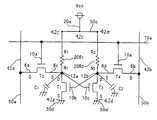
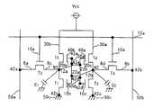
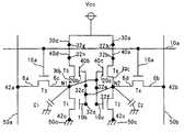
즉, 도 75에 도시된 등가 회로와 같이, 1쌍의 드라이버 MOS 트랜지스터(T1, T2)의 각 드레인 D가 다른 쪽의 MOS 트랜지스터의 게이트 전극 G에 접속되고, 각각의 드레인 D에는 부하 소자, 예컨대, 고저항 폴리실리콘으로 이루어진 부하 저항 R1, R2가 접속되며, MOS 트랜지스터(T1, T2)의 소스 S는 소정의 전위, 예컨대 접지 전위에 고정되고, 부하 저항(R1, R2)의 타단에는 전원 전압 Vcc가 인가되어, MOS 트랜지스터(T1, 52), 부하 저항(R1, R2)으로 이루어진 플립플롭 회로에 미소한 전류를 공급하고 있다. 또, 이 플립플롭 회로의 축적 노드 N1, N2에는 액세스 MOS 트랜지스터(T3, T4)가 접속되어 있다. 이상 4개의 MOS 트랜지스터(T1∼T4)와 2개의 부하 소자(R1, R2)에 의해 1비트의 셀이 구성되어 있다. 또한, 10a는 워드선, 50a, 50b는 비트선을 나타낸다. 도면 중의 그 외의 부호는, 이 후에 구조 및 제조 방법에서 설명하는 부호이고, 회로와 구조와의 대응 관계를 취한 것이다.75, each drain D of the pair of driver MOS transistors T1 and T2 is connected to the gate electrode G of the other MOS transistor, and each drain D is connected to a load element such as, for example, And the load resistors R1 and R2 made of high resistance polysilicon are connected to the power supply voltage Vcc and the sources S of the MOS transistors T1 and T2 are fixed to a predetermined potential, Vcc is applied to supply a minute current to the flip-flop circuit composed of the MOS transistors T1 and 52 and the load resistors R1 and R2. The access MOS transistors T3 and T4 are connected to the accumulation nodes N1 and N2 of the flip-flop circuit. A cell of 1 bit is constituted by the above four MOS transistors (T1 to T4) and two load elements (R1, R2).
도 76은, 부하 소자로서 박막 트랜지스터(TFT:Thin Film Transistor, 이하 필요에 따라서 TFT로 약칭한다)를 이용한 경우의 SRAM 플립플롭 회로의 등가 회로를 나타낸다. 이와 같이 부하 소자에는 일반적으로 고저항 폴리실리콘이나 박막 트랜지스터가 사용되고 있다.76 shows an equivalent circuit of an SRAM flip-flop circuit when a thin film transistor (TFT) is used as a load element (hereinafter abbreviated as TFT if necessary). In general, a high resistance polysilicon or a thin film transistor is used for the load element.
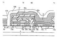
다음에, 도 77∼도 81 및 도 82∼도 86을 이용하여, 종래 기술을 보다 상세하게 설명한다. 도 77∼도 81은 도 75에 나타낸 고저항 부하형의 종래 SRAM의 1비트분의 구조 및 제조 방법을 설명하기 위한 도면이고, 도 77∼도 80은 각 계층마다, 또한 각 공정마다의 1비트분의 평면 레이아웃도를 나타낸 것으로, 도 81은 도 77∼도 80의 Y1-Y2선에 따른 단면도이다.Next, with reference to Figs. 77 to 81 and Fig. 82 to Fig. 86, the prior art will be described in more detail. FIGS. 77 to 81 are views for explaining the structure and manufacturing method of one bit of the high-resistance load type conventional SRAM shown in FIG. 75, Fig. 81 is a sectional view taken along line Y1-Y2 in Figs. 77 to 80. Fig.
도 77은 제1층째 도전막인 게이트 전극을 포함하는 액세스 MOS 트랜지스터 및 드라이버 MOS 트랜지스터의 평면 레이아웃도, 도 78은 다결정 실리콘의 일부에 형성된 고저항 폴리실리콘을 함유하는 제2층째 도전막의 평면 레이아웃도, 도 79는 제3층째 도전막의 평면 레이아웃도, 도 80은 제4층째 도전막인 알루미늄 배선의 평면 레이아웃도이다.77 is a plan layout view of an access MOS transistor and a driver MOS transistor including a gate electrode which is a first layer conductive film and Fig. 78 is a plan layout view of a second layer conductive film containing high resistance polysilicon formed on a part of polycrystalline silicon , Fig. 79 is a plan layout view of the third layer conductive film, and Fig. 80 is a plan layout view of an aluminum wiring which is the fourth layer conductive film.
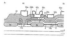
도 77에 있어서 제1층째 도전막인 워드선(10a)은 액세스 MOS 트랜지스터(T3, T4)의 공통 게이트로 되어 있다. 액세스 MOS 트랜지스터(T3, T4)의 드레인 확산층(6a, 6b)은 도 79 및 도 81에 도시된 바와 같이 접속 구멍(21a, 21b)을 통해서 제3층째 도전막(30a, 30b)에 접속되고, 또한 도 80 및 도 81에 도시된 바와 같이 접속 구멍(42a, 42b)을 통해서 제4층째 도전막인 알루미늄 배선 등의 비트선(50a, 50b)에 접속되어 있다.In Fig. 77, the
또, 액세스 MOS 트랜지스터(T3, T4)의 소스(6c, 6d)에는 각각 접속 구멍(5a, 5c)을 통해서 드라이버 MOS 트랜지스터(T2, 51)의 게이트 전극(10b, 10c) 직접 접속되어 있다. 또한, 드라이버 MOS 트랜지스터(T1, T2)의 각 소스는 도 79에 도시된 바와 같이 접속 구멍(21c, 21d)을 통해서 제3층째 도전막(30c)에 의해서 접속되어 있다. 제3층째 도전막(30c)은 메모리내의 모든 드라이버 MOS 트랜지스터의 소스에 접지 전위Vss를 공급하고 있다.The
액세스 MOS 트랜지스터(T3, T4)의 소스 확산층(6c, 6d)은 도 78에 도시된 바와 같이 각각 접속 구멍(12a, 12b)을 통해 저저항 다결정 실리콘(20a, 20b)에 접속되고, 또 고저항부(20R1, 20R2)와 통하고 있다. 또한, 도 78에 도시된 바와 같이, 제2층째 도전막(20c)은 메모리내로의 전원전압 Vcc의 공급선이며, 고저항 소자(r1, r2)에 전원접압을 공급하고 있다.The
다음에, 도 82∼도 86은 도 76에 나타낸 TFT 부하형의 종래 SRAM의 1비트분의 구조 및 제조 방법을 설명하기 위한 도면이고, 도 82∼도 85는 각 계층마다, 또한 각 공정마다의 1비트분의 평면 레이아웃도를 나타내는 것이며, 도 86은 도 82∼도 85의 Y1-Y2선에 따른 단면도이다.Next, Figs. 82 to 86 are diagrams for explaining the structure and manufacturing method for one bit of the conventional SRAM of the TFT load type shown in Fig. 76, and Fig. 82 to Fig. 85 are drawings for each layer, FIG. 86 is a sectional view taken along the line Y1-Y2 in FIGS. 82 to 85. FIG.
도 82는 제1층째 도전막인 게이트 전극을 포함하는 액세스 MOS 트랜지스터 및 드라이버 MOS 트랜지스터의 평면 레이아웃도, 도 83은 제2층째 도전막인 TFT의 하부 게이트 전극의 평면 레이아웃도, 도 84는 제3층째 도전막인 TFT의 채널용의 평면 레이아웃도, 도 85는 제5층째 도전막인 알루미늄 배선의 평면 레이아웃도이다.Fig. 82 is a plan layout view of an access MOS transistor and a driver MOS transistor including a gate electrode which is a first layer conductive film, Fig. 83 is a plan layout view of a bottom gate electrode of a TFT which is a second layer conductive film, 85 is a plan layout view of an aluminum wiring which is a fifth-layer conductive film.
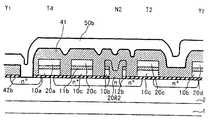
도 82에 있어서, 워드선(10a)은 액세스 MOS 트랜지스터(T3, T4)의 공통 게이트로 되어 있다. MOS 트랜지스터(T4)의 드레인 확산층(6b)은 도 86 및 도 85에 도시된 바와 같이 접속 구멍(32b)을 통해서 제4층째 도전막(40b)에 접속되고, 또 접속 구멍(41b)을 통해 제5층째 도전막인 알루미늄 배선 등의 비트선(50a, 50b)에 접속되어 있다. 동일하게 MOS 트랜지스터(T3)의 드레인 확산층(6a)은 접속 구멍(32a)을 통해서 제4층째 도전막(40a)에 접속되고, 또 접속 구멍(41a)을 통해제5층째 도전막인 알루미늄 배선 등의 비트선(50a, 50b)에 접속되어 있다.In Fig. 82, the
또, MOS 트랜지스터(T3, T4)의 소스(6c, 6d)는 도 82 및 도 86에 도시된 바와 같이, 각각 접속 구멍(5a, 5c)을 통해서 드라이버 MOS 트랜지스터(T2, T1)의 게이트 전극(10b, 10c)에 직접 접속되어 있다. 또한, 드라이버 MOS 트랜지스터(T1, T2)의 소스는 도 82에 도시된 바와 같이, 확산 영역에서 서로 접속되어 있다. 제1층째 도전막(10d)은 메모리내의 모든 드라이버 MOS 트랜지스터의 소스에 접지 전위Vss를 공급하고 있다.The
부하 소자가 되는 TFT:T5, T6은 도 83 및 도 86에 도시된 바와 같이, 제2층째 도전막인 다결정 실리콘으로 형성된 하부 게이트 전극(20a, 20b)과, 도 86에 도시된 바와 같이 제2층째 절연막(21)으로 형성된 게이트 산화막과, 도 84 및 도 86에 도시된 바와 같이 제3층째 도전막인 다결정 실리콘(30a, 30b)으로 형성된 채널에 의해서 구성되어 있다.As shown in FIGS. 83 and 86, the TFTs T5 and T6 serving as load elements are formed of the
도 86 및 도 82∼도 85에 도시된 바와 같이, 액세스 MOS 트랜지스터(T3, T4)의 소스 확산층인 노드N1, N2는 각각 접속 구멍(12a, 21a)에 의해, 또한 접속 구멍(12b, 21b)에 의해 제3층째 도전막인 채널층(30a, 30b)에 접속되어 있다. 채널층(30a, 30b)의 양단은 저저항 다결정 실리콘으로 되어 있고, 타단의 저저항 다결정 실리콘층은 전원전압 Vcc의 공급선으로 되어 있다.The nodes N1 and N2 which are the source diffusion layers of the access MOS transistors T3 and T4 are connected to the
상기와 같은 종래 구조의 SRAM 메모리 셀에서는 다음과 같은 문제점이 있었다.The conventional SRAM memory cell has the following problems.
부하 소자에 이용하는 고저항 폴리실리콘이나 TFT를 메모리 셀상에 적층하는 구조로 형성할 경우, 이들을 드라이버 MOS 트랜지스터(T1, T2)의 게이트 전극(10b, 10c)에 접속 구멍(5a, 5b)을 통해서 직접 접속한다. 이 경우, 접속 구멍(5a, 5b)과 드라이버 MOS 트랜지스터(T1, T2)의 게이트 전극(10b, 10c)간, 드라이버 MOS 트랜지스터(T1, T2)의 게이트 전극(10b, 10c)과 접속 구멍(12a, 12b)간, 또한 접속 구멍(12a, 12b)과 부하 소자와의 사이에서, 각각 사진 제판의 마스크 어긋남이나, 에칭에 의한 치수의 증가(이하 CD 게인이라고 약칭한다)나 치수의 감소(이하 CD 손실이라고 약칭한다)가 생긴다. 이 때문에, 셀 레이아웃을 행할 때에는 충분한 겹침 여유를 확보할 필요가 있으며, 종래형의 메모리 셀에서는 이 겹침 이유가 메모리칩 전체의 면적을 증가시킨다는 문제가 있었다.It is possible to directly connect the
또한, 메모리칩의 밀봉에 이용하는 세라믹 재료나 레진 재료 및 배선 재료 중에 미량으로 포함되어 있는 우라늄(U)이나, 토륨(Th)이 붕괴될 때 α선이 발생한다. 이 α선이 칩 중에 돌입하면, α선의 비정(飛程)에 따라서 전자-정공쌍이 발생하고, 축적 노드N1, n2에 저장된 전하에 혼입하여, 축적 노드N1, N2의 전위를 변동시키며, 이 결과, 메모리 셀의 정보가 파괴된다. 이것이 소프트 에러로 불리는 현상이다. 또한 최근에서는 우주 α선에 의한 소프트 에러도 문제가 되고 있다. 우주 α선이 대기와 충돌하면 중성자가 발생한다. 이 중성자가 칩 중에 돌입하여 Si의 원자핵과 충돌한다. 충돌하면 양자, α입자, 중이온 등의 하전 입자가 발생하는 동시에, Si의 원자핵이 이동한다. 이 때문에, 대량의 전하가 발생하여, 축적 노드 N1, N2에 저장된 전하에 혼입되고, 축적 노드 N1, N2의 전위를 변동시켜서,메모리 셀의 정보를 파괴한다. 종래의 SRAM 메모리 셀에서는 드라이버 MOS 트랜지스터(T1, T2)의 드레인 영역의 n+ 확산층과 p형 실리콘 기판과의 사이에 형성되는 P-N 접합 용량이나, 게이트 산화막이나 층간 절연막 등의 절연막 용량에 의해, α선이 나 중성자에 의한 전하 소실을 보충한 만큼의 전하를 축적할 수 있었다. 그러나 메모리 셀의 면적이 축소되면, α선이나 중성자에 의한 전하 소실을 보충하기에는 축적 전하가 불충분하게 된다. 따라서, 종래의 SRAM 메모리 셀 구조에서는, 미세화하면 소프트 에러율이 증가하고, 메모리의 신뢰성이 현저히 저하한다는 문제가 있다.Further, alpha rays are generated when uranium (U) or thorium (Th) contained in trace amounts in the ceramic material, resin material and wiring material used for sealing the memory chip are collapsed. When this? Line rushes into the chip, electron-hole pairs are generated in accordance with the non-path of the? Line, mixed into the charges stored in the accumulation nodes N1 and n2 to fluctuate the potentials of the accumulation nodes N1 and N2, , Information of the memory cell is destroyed. This is a phenomenon called soft error. In recent years, soft errors due to cosmic α rays also become a problem. When the cosmic α rays collide with the atmosphere, neutrons are generated. This neutron penetrates into the chip and collides with the Si nuclei. Upon collision, charged particles such as protons, alpha particles, and heavy ions are generated, and the atomic nuclei of Si migrate. Therefore, a large amount of charge is generated, mixed into the charges stored in the storage nodes N1 and N2, and the potentials of the storage nodes N1 and N2 are varied to destroy the information of the memory cell. In the conventional SRAM memory cell, due to the PN junction capacitance formed between the n + diffusion layer of the drain region of the driver MOS transistors T1 and T2 and the p-type silicon substrate and the insulating film capacity of the gate oxide film and the interlayer insulating film, It was possible to accumulate as much charge as compensating the charge loss caused by the neutron. However, if the area of the memory cell is reduced, the accumulated charge becomes insufficient to compensate for the charge loss caused by the alpha ray or the neutron. Therefore, in the conventional SRAM memory cell structure, there is a problem that the soft error rate is increased and the reliability of the memory is remarkably lowered.
또한, 부하 소자에 이용하는 고저항 폴리실리콘이나 TFT를 메모리 셀상에 적층하는 구조로 형성할 경우에는, 각 층을 형성할 때마다 사진 제판, 에칭을 행하고 있었다. 따라서, 공정수가 증가하고, 이로 인해, 제품 수율이 저하된다는 문제가 있었다.In addition, when the high-resistance polysilicon or the TFT used for the load element is formed on the memory cell, a photolithography process and an etching process are performed for each layer. Therefore, there is a problem in that the number of steps increases and, consequently, the product yield decreases.
본 발명의 목적은 상술한 바와 같은 종래 기술에 있어서는 문제점을 해결하고, 소요 면적이 작으며, 소프트 에러의 내성이 높고, 종래보다도 제조 공정이 짧은 반도체 장치 및 그 제조 방법을 제공하고자 하는 것이다.SUMMARY OF THE INVENTION An object of the present invention is to provide a semiconductor device and its manufacturing method which solve the problems in the prior art as described above, have a small area, have high resistance to soft errors, and have a shorter manufacturing process than in the prior art.
도 1은 발명의 실시예 1에 따른 SRAM 메모리 셀의 제1층째 및 제2층째 도전막의 평면 레이아웃도.BRIEF DESCRIPTION OF THE DRAWINGS FIG. 1 is a planar layout view of a first layer and a second layer conductive film of an SRAM memory cell according to
도 2는 실시예 1에 따른 제3층째 도전막의 평면 레이아웃도.Fig. 2 is a planar layout view of a third layer conductive film according to the first embodiment; Fig.
도 3은 실시예 1의 도 1 및 도 2의 X1-X2선에 따른 단면도.3 is a sectional view taken along the line X1-X2 in Fig. 1 and Fig. 2 of
도 4는 실시예 1의 도 1 및 도 2의 X1-X2선에 따른 단면도.4 is a sectional view taken along the line X1-X2 in Fig. 1 and Fig. 2 of
도 5는 실시예 1에 따른 SRAM 메모리 셀의 제조 방법을 설명하기 위한 단면도.5 is a sectional view for explaining a method of manufacturing an SRAM memory cell according to the first embodiment;
도 6은 실시예 1에 따른 SRAM 메모리 셀의 제조 방법을 설명하기 위한 단면도.6 is a cross-sectional view illustrating a method of manufacturing an SRAM memory cell according to the first embodiment;
도 7은 실시예 1에 따른 SRAM 메모리 셀의 제조 방법을 설명하기 위한 단면도.7 is a cross-sectional view for explaining a method of manufacturing an SRAM memory cell according to the first embodiment;
도 8은 실시예 1에 따른 SRAM 메모리 셀의 제조 방법을 설명하기 위한 단면도.8 is a cross-sectional view for explaining a method of manufacturing an SRAM memory cell according to the first embodiment;
도 9는 실시예 1에 따른 SRAM 메모리 셀의 제조 방법을 설명하기 위한 단면도.FIG. 9 is a sectional view for explaining a method of manufacturing an SRAM memory cell according to the first embodiment; FIG.
도 10은 실시예 1에 따른 SRAM 메모리 셀의 회로를 설명하기 위한 도면.10 is a diagram for explaining a circuit of an SRAM memory cell according to the first embodiment;
도 11은 본 발명의 실시예 2에 따른 SRAM 메모리 셀의 제1층째 및 제2층째 도전막의 평면 레이아웃도.11 is a planar layout view of first and second layer conductive films of an SRAM memory cell according to
도 12의 실시예 2의 제3층째 도전막의 평면 레이아웃도.Fig. 12 is a planar layout view of the third layer conductive film of Example 2 of Fig. 12; Fig.
도 13은 실시예 2의 제4층째 도전막의 평면 레이아웃도.13 is a planar layout view of a fourth layer conductive film of Example 2. Fig.
도 14는 실시예 2의 도 11∼도 13의 X1-X2선에 따른 단면도.14 is a sectional view taken along the line X1-X2 in Figs. 11 to 13 of
도 15는 실시예 2의 도 11∼도 13의 Y1-Y2선에 따른 단면도.15 is a sectional view taken along the line Y1-Y2 in Figs. 11 to 13 of
도 16은 실시예 2에 따른 SRAM 메모리 셀의 제조 방법을 설명하기 위한 단면도.16 is a sectional view for explaining a method of manufacturing an SRAM memory cell according to the second embodiment;
도 17은 실시예 2에 따른 SRAM 메모리 셀의 제조 방법을 설명하기 위한 단면도.17 is a sectional view for explaining a method of manufacturing an SRAM memory cell according to the second embodiment;
도 18은 실시예 2에 따른 SRAM 메모리 셀의 제조 방법을 설명하기 위한 단면도.18 is a sectional view for explaining a method of manufacturing an SRAM memory cell according to the second embodiment;
도 19는 실시예 2에 따른 SRAM 메모리 셀의 제조 방법을 설명하기 위한 단면도.19 is a sectional view for explaining a method of manufacturing an SRAM memory cell according to a second embodiment;
도 20은 실시예 2에 따른 SRAM 메모리 셀의 제조 방법을 설명하기 위한 단면도.20 is a sectional view for explaining a method of manufacturing an SRAM memory cell according to a second embodiment;
도 21은 실시예 2에 따른 SRAM 메모리 셀의 제조 방법을 설명하기 위한 단면도.21 is a sectional view for explaining a method of manufacturing an SRAM memory cell according to the second embodiment;
도 22는 실시예 2에 따른 SRAM 메모리 셀의 회로를 설명하기 위한 도면.22 is a diagram for explaining a circuit of an SRAM memory cell according to the second embodiment;
도 23은 본 발명의 실시예 3에 따른 SRAM 메모리 셀의 제3층째 도전막의 평면 레이아웃도.23 is a plan layout view of a third layer conductive film of an SRAM memory cell according to
도 24는 실시예 3에 따른 제4층째 도전막의 평면 레이아웃도.24 is a planar layout view of a fourth layer conductive film according to the third embodiment.
도 25는 실시예 3의 도 23∼도 24의 X1-X2선에 따른 단면도.25 is a sectional view taken along the line X1-X2 in Figs. 23 to 24 of the third embodiment; Fig.
도 26은 실시예 3의 도 23∼도 24의 Y1-Y2선에 따른 단면도.26 is a cross-sectional view taken along line Y1-Y2 in Figs. 23 to 24 of
도 27은 실시예 3에 따른 SRAM 메모리 셀의 제조 방법을 설명하기 위한 단면도.27 is a cross-sectional view for explaining a method of manufacturing an SRAM memory cell according to the third embodiment;
도 28은 실시예 3에 따른 SRAM 메모리 셀의 회로를 설명하기 위한 도면.28 is a view for explaining a circuit of an SRAM memory cell according to the third embodiment;
도 29는 실시예 4의 제4층째 도전막의 평면 레이아웃도.29 is a planar layout view of a fourth layer conductive film of the fourth embodiment;
도 30은 실시예 4의 제4층째 도전막의 평면 레이아웃도.30 is a planar layout view of a fourth layer conductive film of the fourth embodiment;
도 31은 실시예 4의 도 30의 X1-X2선에 따른 단면도.31 is a cross-sectional view taken along line X1-X2 of Fig. 30 of
도 32는 실시예 4의 도 30의 Y1-Y2선에 따른 단면도.32 is a sectional view taken along the line Y1-Y2 in Fig. 30 of
도 33은 실시예 4에 따른 SRAM 메모리 셀의 제조 방법을 설명하기 위한 단면도.33 is a sectional view for explaining a method of manufacturing an SRAM memory cell according to a fourth embodiment;
도 34는 실시예 4에 따른 SRAM 메모리 셀의 회로를 설명하기 위한 도면.34 is a diagram for explaining a circuit of an SRAM memory cell according to the fourth embodiment;
도 35는 본 발명의 실시예 5의 SRAM 메모리 셀의 제3층째 및 제4층째 도전막의 평면 레이아웃도.35 is a planar layout view of third and fourth conductive films of the SRAM memory cell according to the fifth embodiment of the present invention;
도 36은 실시예 5의 제 5층째 도전막의 평면 레이아웃도.Fig. 36 is a planar layout view of the fifth layer conductive film of the fifth embodiment. Fig.
도 37은 실시예 5의 도 36의 X1-X2선에 따른 단면도.37 is a sectional view taken along line X1-X2 of Fig. 36 of
도 38은 실시예 5의 도 36의 Y1-Y2선에 따른 단면도.38 is a sectional view taken along line Y1-Y2 of Fig. 36 of
도 39는 실시예 5에 따른 SRAM 메모리 셀의 제조 방법을 설명하기 위한 단면도.FIG. 39 is a sectional view for explaining a method of manufacturing an SRAM memory cell according to a fifth embodiment; FIG.
도 40은 실시예 5에 따른 SRAM 메모리 셀의 제조 방법을 설명하기 위한 단면도.40 is a sectional view for explaining a method of manufacturing an SRAM memory cell according to a fifth embodiment;
도 41은 실시예 5에 따른 SRAM 메모리 셀의 회로를 설명하기 위한 도면.41 is a view for explaining a circuit of an SRAM memory cell according to the fifth embodiment;
도 42는 본 발명의 실시예 6에 따른 SRAM 메모리 셀의 제1층째 도전막의 평면 레이아웃도.42 is a planar layout view of a first layer conductive film of an SRAM memory cell according to
도 43은 실시예 6의 제2층째 및 제3층째 도전막의 평면 레이아웃도.43 is a planar layout view of the second and third conductive films of Example 6;
도 44는 실시예 6의 제4층째 도전막의 평면 레이아웃도.44 is a planar layout view of the fourth layer conductive film of Example 6. Fig.
도 45는 실시예 6의 제5층째 도전막의 평면 레이아웃도.45 is a planar layout view of the fifth layer conductive film of Example 6. Fig.
도 46은 실시예 6의 도 45의 X1-X2선에 따른 단면도.46 is a cross-sectional view taken along the line X1-X2 in Fig. 45 of
도 47은 실시예 6의 도 45의 Y1-Y2선에 따른 단면도.47 is a cross-sectional view taken along line Y1-Y2 of Fig. 45 of
도 48은 실시예 6에 따른 SRAM 메모리 셀의 제조 방법을 설명하기 위한 단면도.48 is a sectional view for explaining a method of manufacturing an SRAM memory cell according to the sixth embodiment;
도 49는 실시예 6에 따른 SRAM 메모리 셀의 제조 방법을 설명하기 위한 단면도.49 is a sectional view for explaining a method of manufacturing an SRAM memory cell according to a sixth embodiment;
도 50은 실시예 6에 따른 SRAM 메모리 셀의 제조 방법을 설명하기 위한 단면도.50 is a sectional view for explaining a method of manufacturing an SRAM memory cell according to a sixth embodiment;
도 51은 실시예 6에 따른 SRAM 메모리 셀의 제조 방법을 설명하기 위한 단면도.51 is a sectional view for explaining a method of manufacturing an SRAM memory cell according to a sixth embodiment;
도 52는 실시예 6에 따른 SRAM 메모리 셀의 제조 방법을 설명하기 위한 단면도.52 is a cross-sectional view for explaining a method of manufacturing an SRAM memory cell according to a sixth embodiment;
도 53은 실시예 6에 따른 SRAM 메모리 셀의 회로를 설명하기 위한 도면.FIG. 53 is a diagram for explaining a circuit of an SRAM memory cell according to the sixth embodiment; FIG.
도 54는 본 발명의 실시예 7에 따른 SRAM 메모리 셀의 제1층째 도전막의 평면 레이아웃도.54 is a planar layout view of a first layer conductive film of an SRAM memory cell according to Embodiment 7 of the present invention.
도 55는 실시예 7의 제2층째 도전막의 평면 레이아웃도.55 is a planar layout view of the second layer conductive film of Example 7. Fig.
도 56은 실시예 7의 제3층째 및 제4층째 도전막의 평면 레이아웃도.56 is a plan layout view of the third and fourth conductive films of Example 7. Fig.
도 57은 실시예 7의 제5층째 도전막의 평면 레이아웃도.57 is a planar layout view of the fifth layer conductive film of Example 7. Fig.
도 58은 실시예 7의 도 57의 X1-X2선에 따른 단면도.58 is a cross-sectional view taken along the line X1-X2 in Fig. 57 of Embodiment 7. Fig.
도 59는 실시예 7의 도 57의 Y1-Y2선에 따른 단면도.59 is a cross-sectional view taken along line Y1-Y2 of Fig. 57 of Embodiment 7. Fig.
도 60은 실시예 7에 따른 SRAM 메모리 셀의 제조 방법을 설명하기 위한 단면도.60 is a sectional view for explaining a method of manufacturing an SRAM memory cell according to a seventh embodiment;
도 61은 실시예 7에 따른 SRAM 메모리 셀의 제조 방법을 설명하기 위한 단면도.61 is a sectional view for explaining a method of manufacturing an SRAM memory cell according to a seventh embodiment;
도 62는 실시예 7에 따른 SRAM 메모리 셀의 제조 방법을 설명하기 위한 단면도.62 is a sectional view for explaining a method of manufacturing an SRAM memory cell according to a seventh embodiment;
도 63은 실시예 7에 따른 SRAM 메모리 셀의 제조 방법을 설명하기 위한 단면도.63 is a cross-sectional view for explaining a method of manufacturing an SRAM memory cell according to a seventh embodiment;
도 64는 실시예 7에 따른 SRAM 메모리 셀의 제조 방법을 설명하기 위한 단면도.64 is a cross-sectional view for explaining a method of manufacturing an SRAM memory cell according to a seventh embodiment;
도 65는 실시예 7에 따른 SRAM 메모리 셀의 회로를 설명하기 위한 도면.65 is a view for explaining a circuit of an SRAM memory cell according to the seventh embodiment;
도 66은 본 발명이 실시예 8에 따른 SRAM 메모리 셀의 제1층째, 제2층째 및 제3층째 도전막의 평면 레이아웃도.66 is a planar layout view of the first, second, and third conductive films of the SRAM memory cell according to the eighth embodiment;
도 67은 실시예 8의 제4층째 도전막의 평면 레이아웃도.67 is a planar layout view of the fourth layer conductive film of the eighth embodiment;
도 68은 실시예 8의 제5층째 도전막의 평면 레이아웃도.68 is a planar layout view of the fifth layer conductive film of Example 8. Fig.
도 69는 실시예 8의 도 68의 X1-X2선에 따른 단면도.69 is a sectional view taken along line X1-X2 in Fig. 68 of Embodiment 8. Fig.
도 70은 실시예 8의 도 68의 X1-X2선에 따른 단면도.70 is a sectional view taken along the line X1-X2 in Fig. 68 of Embodiment 8. Fig.
도 71은 실시예 8에 따른 SRAM 메모리 셀의 제조 방법을 설명하기 위한 단면도.71 is a sectional view for explaining a method of manufacturing an SRAM memory cell according to an eighth embodiment;
도 72는 실시예 8에 따른 SRAM 메모리 셀의 제조 방법을 설명하기 위한 단면도.72 is a sectional view for explaining a method of manufacturing an SRAM memory cell according to an eighth embodiment;
도 73은 실시예 8에 따른 SRAM 메모리 셀의 제조 방법을 설명하기 위한 단면도.73 is a cross-sectional view for explaining a method of manufacturing an SRAM memory cell according to an eighth embodiment;
도 74는 실시예 8에 따른 SRAM 메모리 셀의 회로를 설명하기 위한 도면.74 is a diagram for explaining a circuit of an SRAM memory cell according to an eighth embodiment;
도 75는 저항을 부하 소자로 하는 정적형 랜덤 액세스 메모리의 등가 회로도.75 is an equivalent circuit diagram of a static random access memory in which a resistance is a load element;
도 76은 박막 트랜지스터를 부하 소자로 하는 정적형 랜덤 액세스 메모리의 등가 회로도.76 is an equivalent circuit diagram of a static random access memory having a thin film transistor as a load element.
도 77은 고저항 부하형의 종래 SRAM 메모리 셀의 액세스 MOS 트랜지스터 및 드라이버 MOS 트랜지스터의 평면 레이아웃도.FIG. 77 is a plan layout view of an access MOS transistor and a driver MOS transistor of a conventional SRAM memory cell of a high resistance load type; FIG.
도 78은 고저항 부하형의 종래 SRAM 메모리 셀의 제2층째 도전막의 평면 레이아웃도.78 is a planar layout view of a second layer conductive film of a conventional SRAM memory cell of a high resistance load type;
도 79는 고저항 부하형의 종래 SRAM 메모리 셀의 제3층째 도전막의 평면 레이아웃도.79 is a planar layout view of a third layer conductive film of a high resistance load type conventional SRAM memory cell;
도 80은 고저항 부하형의 종래 SRAM 메모리 셀의 제4층째 도전막의 평면 레이아웃도.80 is a planar layout view of a fourth layer conductive film of a conventional SRAM memory cell of a high resistance load type;
도 81은 고저항 부하형의 종래 SRAM 메모리 셀의 제조 방법 및 구조를 설명하기 위한 단면도.81 is a sectional view for explaining a method and structure for manufacturing a conventional SRAM memory cell of a high resistance load type;
도 82는 TFT 부하형의 종래 SRAM 메모리 셀의 액세스 MOS 트랜지스터 및 드라이버 MOS 트랜지스터의 평면 레이아웃도.82 is a plan layout view of an access MOS transistor and a driver MOS transistor of a conventional SRAM memory cell of a TFT load type;
도 83은 TFT 부하형의 종래 SRAM 메모리 셀의 제2층째 도전막의 평면 레이아웃도.83 is a planar layout view of a second layer conductive film of a conventional SRAM memory cell of a TFT load type.
도 84는 TFT 부하형의 조래 SRAM 메모리 셀의 제3층째 도전막의 평면 레이아웃도.Fig. 84 is a planar layout view of the third layer conductive film of the TFT loaded SRAM memory cell; Fig.
도 85는 TFT 부하형의 종래 SRAM 메모리 셀의 제4층째 도전막의 평면 레이아웃도.85 is a plan layout view of a fourth layer conductive film of a conventional SRAM memory cell of a TFT load type.
도 86은 TFT 부하형의 종래 SRAM 메모리 셀의 제조 방법을 설명하기 위한 단면도.86 is a sectional view for explaining a method of manufacturing a conventional SRAM memory cell of a TFT load type;
<도면의 주요 부분에 대한 부호의 설명>Description of the Related Art
1, 2 : 반도체 기판1, 2: semiconductor substrate
10, 10a, 10b, 10c, 10d : 제1층째 도전막(표면 도전막)10, 10a, 10b, 10c and 10d: a first layer conductive film (surface conductive film)
20, 20a, 20b, 20c, 20d : 제2층째 도전막20, 20a, 20b, 20c and 20d: a second layer conductive film
30, 30a, 30b, 30c, 30d : 제3층째 도전막30, 30a, 30b, 30c, 30d: a third layer conductive film
40, 40a, 40b, 40c, 40d : 제4층째 도전막40, 40a, 40b, 40c and 40d: the fourth layer conductive film
50, 50a, 50b, 50c, 50d : 제4층째 또는 제5층째 도전막50, 50a, 50b, 50c, 50d: the fourth or fifth layer conductive film
4 : 기초 절연막(게이트 절연막)4: basic insulating film (gate insulating film)
11 : 제1층째 절연막11: First layer insulating film
21 : 제2층째 절연막21: Second insulating film
31 : 제3층째 절연막31: Third insulating film
41 : 제4층째 절연막41: Fourth layer insulating film
20R1, 20R2 : 고저항 영역20R1, 20R2: high resistance region
본 발명의 반도체 장치는 반도체 기판의 주면에 접하여 형성된 기초 절연막과, 이 기초 절연막상에 서로 절연막을 사이에 두고 형성된 복수의 도전막을 구비하고, 상기 복수의 도전막 중 인접하는 적어도 2개의 도전막을 절연막에 구멍을 낸 접속 구멍에 의해서 접속하는 동시에 동일한 평면 형상으로 형성한 것을 특징으로하는 것이다.A semiconductor device of the present invention includes a base insulating film formed in contact with a main surface of a semiconductor substrate, and a plurality of conductive films formed on the base insulating film with an insulating film interposed therebetween, wherein at least two adjacent conductive films of the plurality of conductive films And is formed in the same plane shape.
또한, 본 발명의 반도체 장치는 상기 복수의 도전막 중 상기 기초 절연막에 접하여 형성된 도전막을 상기 기초 절연막에 구멍을 낸 접속 구멍에 의해서 상기 반도체 기판에 접속한 것을 특징으로 하는 것이다.The semiconductor device of the present invention is characterized in that a conductive film formed in contact with the base insulating film among the plurality of conductive films is connected to the semiconductor substrate by a connection hole having a hole formed in the base insulating film.
또한, 본 발명의 반도체 장치는 상기 복수의 도전막 중 적어도 하나의 도전막에 고저항 영역을 형성한 것을 특징으로 하는 것이다.Further, the semiconductor device of the present invention is characterized in that a high-resistance region is formed in at least one conductive film of the plurality of conductive films.
또한, 본 발명의 반도체 장치는 상기 복수의 도전막 중의 적어도 하나의 도전막과의 사이에 절연막을 사이에 두어 형성된 다른 도전막을 구비하고, 상기 하나의 도전막과 상기 다른 도전막에 의해 박막 트랜지스터를 형성한 것을 특징으로 하는 것이다.The semiconductor device of the present invention further includes another conductive film formed between the conductive films and at least one of the plurality of conductive films with an insulating film interposed therebetween, Is formed.
또한, 본 발명의 반도체 장치는 상기 하나의 도전막에 의해 상기 박막 트랜지스터의 게이트 전극을 형성하고, 상기 다른 도전막에 의해 상기 박막 트랜지스터의 채널을 형성한 것을 특징으로 하는 것이다.In the semiconductor device of the present invention, the gate electrode of the thin film transistor is formed by the one conductive film, and the channel of the thin film transistor is formed by the other conductive film.
또한, 본 발명의 반도체 장치는 상기 1개의 도전막에 의해 상기 박막 트랜지스터의 채널을 형성하고, 상기 다른 도전막에 의해 상기 박막 트랜지스터의 게이트 전극을 형성한 것을 특징으로 하는 것이다.In the semiconductor device of the present invention, the channel of the thin film transistor is formed by the one conductive film, and the gate electrode of the thin film transistor is formed by the another conductive film.
또한, 본 발명의 반도체 장치는 상기 다른 도전막을 상기 하나의 도전막과의 사이에 절연막을 통해 사이에 두도록 형성하고 또한 상기 하나의 도전막에 접속한 또 다른 도저막을 구비한 것을 특징으로 하는 것이다.The semiconductor device of the present invention is characterized in that the other conductive film is formed so as to be sandwiched between the one conductive film and the insulating film, and another insulating film connected to the one conductive film.
또한, 본 발명의 반도체 장치는 상기 다른 도전막에 의해 박막 트랜지스터의채널을 형성하고, 상기 하나의 도전막과 이것에 접속한 상기 또 다른 도전막에 의해 상기 박막 트랜지스터의 이중 게이트 전극을 형성한 것을 특징으로 하는 것이다.In the semiconductor device of the present invention, the channel of the thin film transistor is formed by the another conductive film, and the one conductive film and the another conductive film connected to the one conductive film form the double gate electrode of the thin film transistor It is characterized by.
또한, 본 발명의 반도체 장치는 상기 다른 도전막과 상기 또 다른 도전막을 동일한 평면 형상(形狀)으로 형성한 것을 특징으로 하는 것이다.The semiconductor device of the present invention is characterized in that the another conductive film and the another conductive film are formed in the same plane shape.
또한, 본 발명의 반도체 장치는 반도체 기판의 주면에 기초 절연막을 사이에두어 형성한 표면 도전막과, 이 표면 도전막상에 서로 절연막을 사이에 두어 형성한 복수의 도전막을 구비하고, 상기 복수의 도전막 중 적어도 2개의 도전막을 동일평면 형상으로 형성하며, 또한 그 한쪽의 도전막과 상기 표면 도전막을 절연막에 구멍을 낸 접속 구멍에 의해서 접속한 것을 특징으로 하는 것이다.A semiconductor device according to the present invention includes a surface conductive film formed on a main surface of a semiconductor substrate with a base insulating film therebetween and a plurality of conductive films formed on the surface conductive film with an insulating film interposed therebetween, At least two of the conductive films are formed in the same plane shape, and one of the conductive films and the surface conductive film are connected by a connection hole having a hole formed in the insulating film.
또한, 본 발명의 반도체 장치는 상기 표면 도전막을 상기 기초 절연막에 구멍을 낸 접속 구멍에 의해서 상기 반도체 기판에 접속한 것을 특징으로 하는 것이다.The semiconductor device of the present invention is characterized in that the surface conductive film is connected to the semiconductor substrate by a connection hole having a hole formed in the base insulating film.
또한, 본 발명의 반도체 장치는 상기 복수의 도전막 중 적어도 하나의 도전막에 고저하 영역을 형성한 것을 특징으로 하는 것이다.Further, the semiconductor device of the present invention is characterized in that a high-reduction region is formed in at least one conductive film among the plurality of conductive films.
또한, 본 발명의 반도체 장치는 상기 2개의 도전막 중의 상기 한쪽의 도전막에 의해 박막 트랜지스터의 게이트 전극을 형성하고, 상기 2개의 도전막 중의 다른 쪽의 도전막에 의해 상기 박막 트랜지스터의 채널을 형성한 것을 특징으로 하는 것이다.In the semiconductor device of the present invention, the gate electrode of the thin film transistor is formed by the one conductive film of the two conductive films, and the channel of the thin film transistor is formed by the other conductive film of the two conductive films .
또한, 본 발명의 반도체 장치는 상기 2개의 도전막 중의 다른쪽의 도전막을절연막을 통해 상기 한쪽의 도전막과의 사이에 두도록 형성되며 또한 상기 한쪽의 도전막에 접속된 또 다른 도전막을 구비하는 것을 특징으로 하는 것이다.The semiconductor device of the present invention further includes another conductive film formed so that the other conductive film of the two conductive films is sandwiched between the conductive film and the one conductive film through an insulating film It is characterized by.
또한, 본 발명의 반도체 장치는 상기 2개의 도전막 중의 다른쪽의 도전막에 의해 박막 트랜지스터의 채널을 형성하고, 상기 한쪽의 도전막과 이것에 접속된 상기 또 다른 도전막에 의해 상기 박막 트랜지스터의 이중 게이트 전극을 형성한 것을 특징으로 하는 것이다.In the semiconductor device of the present invention, the channel of the thin film transistor is formed by the other conductive film of the two conductive films, and the channel of the thin film transistor is formed by the one conductive film and the another conductive film connected to the one conductive film. And a double gate electrode is formed.
다음에, 본 발명의 반도체 장치의 제조 방법은 반도체 기판의 기초 절연막상에 제1 도전막을 형성하는 공정과, 상기 제1 도전막상에 제1 절연막을 형성하는 공정과, 적어도 상기 제1 절연막 및 상기 제1 도전막을 관통하는 트인 구멍을 형성하는 공정과, 상기 트인 구멍을 포함하는 상기 제1 절연막상에 제2 도전막을 형성하는 공정과, 상기 제2 도전막, 상기 제1 절연막 및 상기 제1 도전막을 동일 평면 형상으로 패터닝하는 공정을 포함하는 것을 특징으로 하는 것이다.Next, a method of manufacturing a semiconductor device according to the present invention comprises the steps of: forming a first conductive film on a base insulating film of a semiconductor substrate; forming a first insulating film on the first conductive film; A step of forming a first hole penetrating through the first conductive film, a step of forming a second conductive film on the first insulating film including the hole, and a step of forming the second conductive film, And patterning the film in the same plane shape.
또한, 본 발명의 반도체 장치의 제조 방법은 반도체 기판의 주면에 기초 절연막을 형성하는 공정과, 상기 기초 절연막상에 제1 도전막을 형성하는 공정과, 상기 제1 도전막상에 제1 절연막을 형성하는 공정과, 상기 제1 절연막, 상기 제1 도전막, 및 상기 기초 절연막을 관통하는 트인 구멍을 형성하는 공정과, 상기 트인 구멍을 포함하고 상기 제1 절연막상에 제2 도전막을 형성하는 공정과, 상기 제2 도전막, 상기 제1 절연막, 상기 제1 도전막 및 상기 기초 절연막을 동일 평면 형상으로 패터닝하는 공정을 포함하는 것을 특징으로 하는 것이다.A method of manufacturing a semiconductor device according to the present invention includes the steps of forming a base insulating film on a main surface of a semiconductor substrate, forming a first conductive film on the base insulating film, forming a first insulating film on the first conductive film A step of forming a through hole through the first insulating film, the first conductive film, and the base insulating film; a step of forming a second conductive film on the first insulating film, And patterning the second conductive film, the first insulating film, the first conductive film, and the base insulating film in the same plane shape.
또한, 본 발명의 반도체 장치의 제조 방법은 반도체 기판의 주면에 기초 절연막을 형성하는 공정과, 상기 기초 절연막상에 제1 도전막을 형성하는 공정과, 상기 제1 도전막상에 제1 절연막을 형성하는 공정과, 상기 제1 절연막, 상기 제1 도전막 및 상기 기초 절연막을 관통하는 트인 구멍을 형성하는 공정과, 상기 트인 구멍을 포함하고 상기 제1 절연막상에 제2 도전막을 형성하는 공정과, 상기 제2 도전막상에 제2 절연막을 형성하는 공정과, 상기 제2 절연막상에 제3 도전막을 형성하는 공정과, 상기 트인 구멍을 포함하도록 상기 제3 도전막, 상기 제2 절연막, 상기 제2 도전막, 상기 제1 절연막 및 상기 제1 도전막을 동일한 평면 형상으로 패터닝하는 공정을 포함하는 것을 특징으로 하는 것이다.A method of manufacturing a semiconductor device according to the present invention includes the steps of forming a base insulating film on a main surface of a semiconductor substrate, forming a first conductive film on the base insulating film, forming a first insulating film on the first conductive film A step of forming a through hole through the first insulating film, the first conductive film, and the base insulating film; a step of forming a second conductive film on the first insulating film including the first hole, A step of forming a second insulating film on the second conductive film, a step of forming a third conductive film on the second insulating film, and a step of forming the third conductive film, the second insulating film, And patterning the first insulating film and the first conductive film in the same planar shape.
또한, 본 발명의 반도체 장치의 제조 방법은 반도체 기판의 주면에 기초 절연막을 형성하는 공정과, 상기 기초 절연막에 기초 트인 구멍을 형성하는 공정과, 상기 기초 트인 구멍을 포함하는 상기 기초 절연막상에 제1 도전막을 형성하는 공정과, 상기 제1 도전막을 패터닝하는 공정과, 상기 제1 도전막 및 상기 기초 절연막상에 제1 절연막을 형성하는 공정과, 상기 제1 절연막상에 제1 트인 구멍을 형성하는 공정과, 상기 제1 트인 구멍을 포함하는 상기 제1 절연막상에 제2 도전막을 형성하는 공정과, 상기 제2 도전막상에 제2 절연막을 형성하는 공정과, 상기 제2 절연막상에 제3 도전막을 형성하는 공정과, 상기 제3 도전막, 상기 제2 절연막 및 상기 제2 도전막을 동일 평면 형상으로 패터닝하는 공정을 포함하는 것을 특징으로 하는 것이다.A method of manufacturing a semiconductor device according to the present invention includes the steps of forming a base insulating film on a main surface of a semiconductor substrate; forming holes in the base insulating film; 1. A method for manufacturing a semiconductor device, comprising the steps of: forming a conductive film; patterning the first conductive film; forming a first insulating film on the first conductive film and the base insulating film; A step of forming a second conductive film on the first insulating film including the first insulating film, a step of forming a second insulating film on the second conductive film, a step of forming a third insulating film on the third insulating film, A step of forming a conductive film, and a step of patterning the third conductive film, the second insulating film and the second conductive film in the same plane shape.
또한, 본 발명의 반도체 장치의 제조 방법은 반도체 기판의 주면에 기초 절연막을 형성하는 공정과, 상기 기초 절연막에 기초 트인 구멍을 형성하는 공정과,상기 기초 트인 구멍을 포함하는 상기 기초 절연막상에 제1 도전막을 형성하는 공정과, 상기 제1 도전막을 패터닝하는 공정과, 상기 제1 도전막 및 상기 기초 절연막상에 제1 절연막을 형성하는 공정과, 상기 제1 절연막에 제1 트인 구멍을 형성하는 공정과, 상기 제1 트인 구멍을 포함하는 상기 제1 절연막상에 제2 도전막을 형성하는 공정과, 상기 제2 도전막을 패터닝하는 공정과, 상기 제2 도전막 및 상기 제1 절연층상에 제2 절연막을 형성하는 공정과, 상기 제2 절연막에 제2 트인 구멍을 형성하는 공정과, 상기 제2 트인 구멍을 포함하는 상기 제2 절연막상에 제3 도전막을 형성하는 공정과, 상기 제3 도전막상에 제3 절연막을 형성하는 공정과, 상기 제3 절연막상에 제4 도전막을 형성하는 공정과, 상기 제4 도전막, 상기 제3 절연막 및 상기 제3 도전막을 동일 평면 형상으로 패터닝하는 공정을 포함하는 것을 특징으로 하는 것이다.A method of manufacturing a semiconductor device according to the present invention includes the steps of forming a base insulating film on a main surface of a semiconductor substrate; forming holes in the base insulating film; Forming a first insulating film on the first conductive film and the base insulating film, forming a first insulating film on the first insulating film, forming a first insulating film on the first insulating film, Forming a second conductive film on the first insulating film including the first hole, patterning the second conductive film, and forming a second insulating film on the second insulating film, Forming a second insulating film on the second insulating film; forming a second insulating film on the second insulating film; forming a third insulating film on the second insulating film including the second insulating film; Forming a third insulating film on the first insulating film, forming a fourth insulating film on the third insulating film, patterning the fourth conductive film, the third insulating film, and the third conductive film in the same planar shape And a control unit.
이하, 본 발명의 실시예에 의한 반도체 장치츨, SRAM 메모리 셀을 예로 들어 설명한다. 또, 각 도면에 있어서 동일한 부호는 동일하게 또는 상당 부분을 나타낸다.Hereinafter, a semiconductor device according to an embodiment of the present invention and an SRAM memory cell will be described as an example. In the drawings, the same reference numerals denote the same or substantially equivalent parts.
실시예 1Example 1
이 실시의 형태1은, SRAM 메모리 셀의 부하 소자가 고저항 소자로 구성되고, 또한 MOS 트랜지스터의 게이트 전극과 저항 소자가 동시에 동일 평면 형상으로 형성되어 있는 것에 특징이 있다.The first embodiment is characterized in that the load element of the SRAM memory cell is constituted by a high resistance element, and the gate electrode and the resistance element of the MOS transistor are simultaneously formed in the same plane shape.
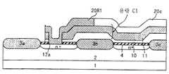
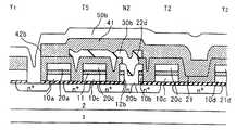
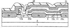
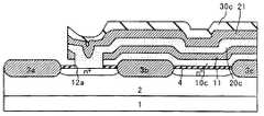
도 1∼도 10은 실시예 1에 따른 SRAM 메모리 셀의 구조와 제조 방법을 설명하기 위한 도면이다. 도 1 및 도 2는 SRAM 메모리 셀의 평면 레이아웃을 설명하기위한 도면이고, 도 1은 제1층째 도전막 즉 MOS 트랜지스터의 게이트 전극과, 제2층째 도전막 즉 고저항 소자의 평면 레이아웃도이다. 또한, 도 2는 제3층째 도전막 즉 알루미늄 배선의 평면 레이아웃도이다.1 to 10 are views for explaining a structure and a manufacturing method of an SRAM memory cell according to the first embodiment. 1 and 2 are views for explaining a plan layout of an SRAM memory cell. FIG. 1 is a plan layout view of a gate electrode of a first layer conductive film, that is, a MOS transistor, and a second layer conductive film, that is, a high resistance element. 2 is a plan layout view of the third layer conductive film, that is, the aluminum wiring.
또한, 도 3 및 도 4는 각각 도 1 및 도 2의 평면 레이아웃도의 X1-X2, Y1-Y2선에 따른 단면을 나타내는 도면이다. 또한, 도 5∼도 9는 SRAM 메모리 셀의 제조방법을 설명하기 위한 도면으로서, 도 1 및 도 2의 평면 레이아웃도의 X1-X2선의 단면에서의 제조 공정을 나타내는 도면이다.3 and 4 are views each showing a cross section taken along the line X1-X2 and Y1-Y2 in the plan layout view of Figs. 1 and 2, respectively. Figs. 5 to 9 are drawings for explaining a method of manufacturing an SRAM memory cell, and show manufacturing steps in a cross-section taken along a line X1-X2 in the plan layout diagrams of Figs. 1 and 2. Fig.
또한, 도 10은 실시예 1에 따른 SRAM의 회로와 구조의 대응을 설명하기 위한 도면이다.10 is a diagram for explaining the correspondence between the circuit and the structure of the SRAM according to the first embodiment.
다음에, 이 실시예 1에 따른 메모리 셀에 대해, 도 1∼도 10을 참조하여 제조 방법에 관해 설명하고 아울러 그 구조에 관해서 설명한다.Next, a method of manufacturing the memory cell according to the first embodiment will be described with reference to Figs. 1 to 10, and its structure will be described.
먼저, 도 5를 참조하여 비저항 10Ω·㎝(100)면의 n형 실리콘 기판(1)내에 불순물 농도 1.0E15∼1.0E17/㎤의 P형 웰(2)(반도체 기판의 일부로서의 웰2. 이하 동일함)을 붕소 이온 주입과 열확산법에 의해 형성한다.First, referring to Fig. 5, a p-type well 2 (a well 2 as a part of a semiconductor substrate) having an impurity concentration of 1.0E15 to 1.0E17 / cm3 is formed in an n-
다음에, LOCOS법 등에 의해 두께 100∼1000㎚의 실리콘 산화막(3a,3b,3c)을 형성하고, MOS 트랜지스터의 형성 영역을 절연분리한다.Next,
다음에, 레지스트(3′)를 도포하고 포토리소그래피를 이용하여, 실리콘 산화막(3b과3c)의 사이에서, 후에 형성하는 액세스 MOS 트랜지스터(T4)의 소스 영역의 일부로서, 제1층째 도전막(10c)의 하부 영역이 되는 부분에는, 비소 등의 n형 불순물의 이온 주입을 행하지 않는 n+ 영역을 형성한 후, 레지스트(3′)를 제거한다.Next, a resist 3 'is applied and photolithography is performed to form a first layer conductive film (a first conductive film) as a part of a source region of the access MOS transistor T4 to be formed later between the
다음에, 도 6을 참조하여 MOS 트랜지스터의 능동 영역이 되는 부분에 두께 10∼100㎚의 게이트 산화막(4)(기초 절연막)을 형성한다.Next, referring to FIG. 6, a gate oxide film 4 (base insulating film) having a thickness of 10 to 100 nm is formed in a portion which becomes an active region of the MOS transistor.
다음에, 도 7을 참조하여, 인 드의 n형 불순물을 포함하는 다결정 실리콘막, 금속 실리사이드막 또는 금속 폴리사이드막 등의 도전막을 이영한 제1층째 도전막(10)(표면 도전막)을 퇴적하고, 또 이어서 SiO2등으로 이루어진 제1층째 층간 절연막(11)을 두께 100∼1000㎚로 퇴적한다.Next, referring to Fig. 7, a first layer conductive film 10 (surface conductive film) formed by depositing a conductive film such as a polycrystalline silicon film, a metal silicide film or a metal polycide film containing indium n-type impurity is deposited And then the first
다음에, 도 8 및 도 1을 참조하여, 포토리소그래피와 에칭에 의해 제1층째 층간 절연막(11), 제1층째 도전막(10) 및 게이트 산화막(4)을 동시 구멍을 내어, 층간 접속 구멍(12a,12b)을 형성한다. 다음에, 다결정 실리콘막 등에 의한 제2층째 도전막(20)을 퇴적하고, 이 도전막(20)의 표면에 도우즈량 1.0E12∼1.3E13/㎠으로 인 등의 n형 불순물의 이온 주입을 행한다.Next, referring to FIG. 8 and FIG. 1, the first-layer
다음에, 도 9 및 도 1를 참조하여, 포토리소그래피와 에칭에 의해, 접속 구멍(12a,12b)을 통한 층간 접속을 포함하도록, 제2층째 도전막(20), 제1층째 층간 절연막(11) 및 제1층째 도전막(10)을 동시에 패터닝하고, 제1층째 도전막(10a,10b,10c,10d) 및 제2층째 도전막(20a,20b,20c,20d)을 형성한다.Next, with reference to FIG. 9 and FIG. 1, the second layer
제1층째 도전막(10a)은 액세스 MOS 트랜지스터(T3,T4)에 공통 게이트 전극 또한 워드선이 되고, 도전막(10b,10c)은 각각 드라이버 MOS 트랜지스터(T1,T2)의 게이트 전극이 되며, 또한 도전막(10d)은 인접한 메모리 셀의 액세스 MOS 트랜지스터의 게이트 전극이 되는 것이다.The first layer
제2층째 도전막(20a,20d)은 전원전위의 공급선이 되고, 도전막(20b,20c)은 저항 소자(20R1 및 20R2)를 형성하는 부하 회로가 되기 위한 것이다.The second layer
다음에, 이와 같이 패터닝한 것에 대하여, 포토리소그래피를 마스크로 하여, 비소 등의 n형 불순물의 이온 주입에 의해, MOS 트랜지스터(T1∼T4)의 소스/드레인 영역을 형성하는 동시에, 제2층째 도전막(20b,20c)을 저항 소자(20R1 및 20R2)의 부분을 제외하고 저저항으로 형성한다.Next, the source / drain regions of the MOS transistors T1 to T4 are formed by ion implantation of n-type impurities such as arsenic using photolithography as a mask, The
다음에, 도 3, 도 4 및 도 2를 참조하여, CVD법 등에 의해, SiO2등의 절연막(41)을 두께 100∼1000㎚로 퇴적한다. 이어서, 절연막(41)에 접속 구멍(42a∼42e)을 구멍을 낸 후, 제3층째 도전막으로서 알루미늄 배선(50a∼50d)을 500 ∼ 2000㎚의 두께로 형성한다. 알루미늄 배선(50a,50b)은 비트선이 되고, 알루미늄 배선(50c)은 전원전위 공급선이 되며, 알루미늄 배선(50d)은 접지 전위 공급선이 된다.Next, referring to FIG. 3, FIG. 4, and FIG. 2, an insulating
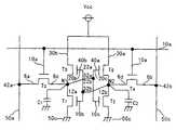
이와 같이 형성된 메모리 셀에 관해서, 도 10과 같이 회로가 형성되는 것을 구조와 관련지어서 설명한다. 도 10의 회로도에서 도 1∼도 9의 구조의 부호에 대응한 부호가 붙어 있다.With respect to the memory cell thus formed, a circuit is formed as shown in Fig. In the circuit diagram of Fig. 10, reference numerals corresponding to the reference numerals of the structures of Figs. 1 to 9 are attached.
먼저, 도 1에 도시된 바와 같이, 제1 도전막(10a)은 액세스 MOS 트랜지스터(T3,T4)의 공통 게이트가 되고, 또한 워드선이 된다.First, as shown in Fig. 1, the first
액세스 MOS 트랜지스터(T3,T4)의 드레인 확산층(6a,6b)은 도 2에 도시된 바와 같이, 각각 접속 구멍(42a,42b)을 통해서 비트선의 알루미늄 배선(50a,50b)과접속되어 있다.The
액세스 MOS 트랜지스터(T3)의 소스(6c)는 도 1에 도시된 바와 같이 확산층에서 노드N1에 연결되고, 노드N1은 도 3에 도시된 바와 같이 게이트 산화막(4)이 일부 에칭된 구멍(12a)을 통해서 제1 도전막(10c)과 직접 접속되며, 이것은 연장되어 드라이버 MOS 트랜지스터(T2)의 게이트로 되어 있다.The
또한, 노드N1은 접속 구멍(12a)을 통해서 저항(20R1)과 접속되고, 또 저항(20R1)은 접속 구멍(42c)을 통해서 제3층째 도전막인 전원전위 공급선(50c)에 접속된다. 전원전위 공급선(50c)은 다른 접속 구멍(42c)을 통해서 워드선(10a)상에 있는 전원전위 공급선(20a)에 접속되어 있다. 전원전위 공급선(20a)의 전원전압Vcc로부터 공급되는 미소 전류는 고정항부(20R1)를 통해서 액세스 MOS 트랜지스터 (T3)의 소스층(6c)에 흐른다.The node N1 is connected to the resistor 20R1 through the
또한, 제2층째 도전막(20c)은 제1층째 도전막(100)과 층간 절연막(11)에 의해 용량 소자(C1)를 형성하고 있으며, 축적 노드N1의 확산층(6c)에 전하를 공급할 수 있다.The second layer
또한, 노드N1은 확산층에 의해 드라이버 MOS 트랜지스터(T1)의 드레인과 접속하고 있다.The node N1 is connected to the drain of the driver MOS transistor T1 by the diffusion layer.
다음에, 액세스 MOS 트랜지스터(T4)의 소스(6d)는 확산층에 의해 노드N2에 연결되고, 노드 N2는 게이트 산화막(4)이 일부 에칭된 구멍(12b)을 통해서 제1 도전막(10b)과 집적 접속되고, 이것은 연장되어 드라이버 MOS 트랜지스터(T1)의 게이트로 되어 있다.Next, the
또한, 노드N2는 도 4 및 도 1에 도시된 바와 같이, 저항(20R2)에 접속하고, 저항(20R2)은 도 2로부터 알 수 있는 바와 같이 접속 구멍(42e)을 통해서 전원전위 공급선(50c)에 접속되어 있다.The node N2 is connected to the resistor 20R2 as shown in Fig. 4 and Fig. 1 and the resistor 20R2 is connected to the power supply
또한, 노드N2는 확산층에 의해 드라이버 MOS 트랜지스터(T2)의 드레인과 접속하고 있다.The node N2 is connected to the drain of the driver MOS transistor T2 by a diffusion layer.
또한, 드라이버 MOS 트랜지스터(T1)의 소스S와 드라이버 MOS 트랜지스터(T2)의소스S와는 도 1에 도시된 바와 같이 확산 영역에서 연통(連通)하고 잇고, 이것은 도 2로부터 알 수 있는 바와 같이 접속 구멍(42d)을 통해 접지전위 공급선인 알루미늄 배선(50d)에 접속되어 있다. 알루미늄 배선(50d)은 접지전위Vss에 고정되어 있으며, 기억 장치내의 모든 드라이버 MOS 트랜지스터의 소스에 접속되어 있다. 이상과 같이 하여, 도 10의 회로가 형성되어 있다.The source S of the driver MOS transistor T1 and the source S of the driver MOS transistor T2 communicate with each other in the diffusion region as shown in Fig. 1, And is connected to the
이상 설명한 바와 같이, 이 실시예 1에 의하면, 제2층째 도전막(20), 제 1층째 층간 절연막(11) 및 제1층째 도전막(10)을, 필요한 층간 접속을 포함하도록 동시에 패터닝하여 동일 평면 형상에 형성하기 때문에, 종래 필요하던 겹침 여유가 불필요해지고, 메모리 셀 치수의 세로 방향, 가로 방향의 길이를 각각 축소할 수 있다.As described above, according to the first embodiment, the second layer
또한, 제1층째 층간 절연막(11), 제1층째 도전막(10) 및 게이트 산화막(4)을 동시에 구멍을 내어, 접속 구멍(12a,12b)을 형성한 후, 제2층째 도전막(20)으로서 다결정 실리콘막 등 도전막을 퇴적하여, 제2층째 도전막(20) 및 제1층째 도전막(10)을 축적 노드N1,N2에 접속하고 있기 때문에, 제2층째 도전막(20), 제1층째 층간 절연막(11) 및 제1층째 도전막(10)으로 형성되는 용량 소자(C1,C2)의 정전 용량을 각각 축적 노드N1,N2에 접속할 수 있기 때문에,α선이나 중성자에 대한 내성을 크게할 수 있다.After the connection holes 12a and 12b are formed by piercing the first layer
또, 제2층째 도전막(20), 제1층째 층간 절연막(11) 및 제1층째 도전막(10)을 동시에 패터닝하여 형성하기 때문에, 종래 필요하던 이온 주입 공정, 포토리소그래피 공정, 에칭 공정 등의 저항 소자 형성 공정이 불필요해지고, 공정수를 약 15% 이상 삭감할 수 있다.Since the second-layer
실시예 2Example 2
이 실시예 2는 SRAM 메모리 셀의 부하 소자가 하부 게이트 구조의 TFT로 구성되고, 또한 MOS 트랜지서터의 게이트 전극과 TFT의 하부 게이크 전극이 동시에 동일 평면 형상에 형성되어 있은 것에 특징이 있다.The second embodiment is characterized in that the load element of the SRAM memory cell is constituted by the TFT of the lower gate structure and the gate electrode of the MOS transistor and the lower gate electrode of the TFT are simultaneously formed in the same plane shape.
도 11∼도 22는 실시예 2에 따른 반도체 장치의 일예로서 SRAM 메모리 셀의 구조와 제조 방법을 설명하기 위한 도면이다.11 to 22 are views for explaining a structure and a manufacturing method of an SRAM memory cell as an example of the semiconductor device according to the second embodiment.
도 11∼도 13은 SARM 메모리 셀이 평면 레이아웃을 설명하기 위한 도면이고, 도 11은 제1층째 도전막 즉 MOS 트랜지스터의 게이트 전극과, 제2층째 도전막 즉 TFT의 하부 게이트 전극의 평명 레이아웃도이다. 도 12는 제3층째 도전막 즉 TFT의 채널층의 평면 레이아웃도이다. 또한, 도 13은 제4층째 도전막 즉 알루미늄 배선의 평먼 레이아웃도이다.Figs. 11 to 13 are diagrams for explaining a planar layout of the SARM memory cell, Fig. 11 is a plan view of the gate electrode of the first layer conductive film, that is, the MOS transistor and the flat gate layout of the second layer conductive film, to be. 12 is a plan layout view of the channel layer of the third conductive film, that is, the TFT. 13 is a plain layout of the fourth layer conductive film, that is, aluminum wiring.
또한, 도 14 및 도 15는 각각 도 11∼도 13의 평면 레이아웃도의 X1-X2, Y1-Y2선에 따른 단면을 나타내는 도면이다. 또한, 도 16∼도 21은 SRAM 메모리 셀의제조 방법을 설명하기 위한 도면이고, 도 11∼도 13은 평면 레아아웃도의 X1-X2선의 단면에서의 제조 공정을 나타내는 도면이다.Figs. 14 and 15 are views each showing a cross section taken along line X1-X2 and Y1-Y2 in the plan layout diagrams of Figs. 11 to 13, respectively. FIGS. 16 to 21 are diagrams for explaining a method of manufacturing an SRAM memory cell, and FIGS. 11 to 13 are diagrams showing manufacturing steps in the cross section of the X1-X2 line of the planar layout.
또한, 도 22는 이 실시예 2에 따른 SRAM의 회로와 구조와의 대응 관계를 설명하기 위한 도면이다.22 is a diagram for explaining a correspondence relationship between the circuit and the structure of the SRAM according to the second embodiment.
다음에, 이 실시예 2의 메모리 셀에 관해서는, 도 17∼도 22를 참조하여 제조 방법에 대해 설명하고, 아울러 그 구조에 관해서 설명한다.Next, the manufacturing method of the memory cell of the second embodiment will be described with reference to Figs. 17 to 22, and its structure will be described.
먼저, 도 16을 참조하여, 비저항10Ω·㎝(100)면의 n형 실리콘 기판(1)내에 불순물 농도 1.0E15∼1.0E17/㎤의 P형의 웰(2)을 붕소의 이온 주입과 열확산법에 의해 형성한다. 다음에, LOCOS법 등에 의해 두께 100∼1000㎚의 실리콘 산화막(3a,3b,3c)을 형성하여, MOS 트랜지스터의 형성 영역을 절연불리한다.First, referring to FIG. 16, a P-type well 2 having an impurity concentration of 1.0E15 to 1.0E17 / cm3 is implanted into an n-
다음에, 레지스트(3′)를 도포하고, 포토 리소그래피를 이용하여, 실리콘 산화막(3b와 3c)의 사이에서, 후에 형성하는 액세스 MOS 트랜지스터(T4)의 소스 영역의 일부로서, 제1층째 도전막(10c)의 하부 영역이 되는 부분에만, 비소 등의 n형 불순물의 이온 주입을 행하여 n+영역을 형성한 후, 레지스트(3′)를 제거한다.Next, a resist 3 'is applied and, as a part of the source region of the access MOS transistor T4 to be formed later, between the
다음에, 도 17을 참조하여, MOS 트랜지스터의 능동 영역이 되는 부분에 두께10∼100㎚의 게이트 산화막(4)을 형성한다.Next, referring to Fig. 17, a
도 18을 참조하여, 다음에, 인 등의 n형 불순물을 함유하는 다결정 실리콘막, 금속 실리사이트막, 또는 금속 폴리사이드막 등의 도전막을 이용한 제1층째 도전막(10)을 축적하고, 또 이어서 SiO2등으로 이루어진 제1층째 층간 절연막(11)을두께 100∼1000㎚로 퇴적한다.18, next, a first layer
도 19 및 도 11을 참조하고, 다음에, 포토 리소그래피와 에칭에 의해 제1층째 층간 절연막(11), 제1층째 도전막(10) 및 게이트 산화막(4)을 동시 구멍을 내어, 층간 접속 구멍(12a,12b)을 형성한다. 다음에, 다결정 실리콘막 등에 의한 제2층째 도전막(20)을 퇴적하고, 이 도전막(20)의 표면에 도우즈량 1.0E12∼10E13/㎠로 인 등의 n형 불순물의 이온 주입을 행한다.19 and 11, the first-layer
도 20 및 도 11을 참조하고, 다음에 포토 리소그래피와 에칭에 의해, 접속 구멍(12a,12b)을 통한 층간 접속을 포함하는 바와 같이, 제2층째 도전막(20), 제1층째 층간 절연막(11) 및 제1층째 도전막(10)을 동시에 패터닝하고, 제1층째 도전막(10a,10b,10c,10d)과 제2층째 도전막(20a,20b,20c,20d)을 동일 평면 형상으로 형성한다.20 and 11 and then subjected to photolithography and etching to form a second layer
제1층째 도전막(10a)은 액세스 MOS 트랜지스터(T3,T4)에 공통의 게이트 전극 또한 워드선이 되고, 도전막(10b,10c)은 각각 드라이버 MOS 트랜지스터(T1,T2)의 게이트 전극이 되며, 또 도전막(10d)은 인접한 셀의 액세스 MOS 트랜지스터의 게이트 전극이 되는 것이다.The first layer
제2층째 도전막(20b,20c)은 TFT의 하부 게이트 전극을 형성하기 위한 것이다. 도전막(20a,20d)은 후에 형성하는 절연막을 통하여 용량을 형성한다.The second-layer
다음에, 이와 같이 패터닝한 것에 대하여, 포토 리소그래피를 마스크하여, 비소 등의 n형 불순물의 이온 주입에 의해, MOS 트랜지스터(T1∼T4)의 소스/드레인 영역을 형성하는 동시에, 제2층째 도전막(20a∼20d)을 저저항으로 형성한다.Next, with respect to the patterning thus conducted, the source / drain regions of the MOS transistors T1 to T4 are formed by ion-implanting n-type impurities such as arsenic by photolithography, (20a to 20d) are formed with a low resistance.
도 21을 참조하고, 다음에, SiO2등의 제2층째 층간 절연막(21)을 두께 100∼1000㎚으로 퇴적한다. 다음에, 도 12를 함께 참조하여, 포토 리소그래피와 에칭에 의해 제2층째 층간 절연막(21)을 구멍을 내어, 층간 접속 구멍(22a,22b)을 형성한다. 또, 이전에 설명한 접속 구멍(12a,12b)을 접속 구멍(22a,22b)으로 대용하는 것도 가능하다. 그 경우, 접속 구멍(12a,12b)은 불필요해진다.Referring to FIG. 21, a second-layer
다음에, 다결정 실리콘막 등에 의한 제3층째 도전막(30)(30a,30b을 포함함)을 퇴적하고, 포토 리소그래피와 에칭에 의해 TFT의 채널이 되며, 또한 전원전압Vcc의 급전용 배선이 되는 제3층째 도전막(30a,30b)을 형성한다. 다음에, 이 도전막(30a,30b)의 표면에 도우즈량1.0E12∼1.0E12/㎠로 붕소 등의 p형 불순물의 이온주입을 행하여 TFT의 채널 영역을 형성한다. 다음에 포토 리소그래피를 마스크하여, 붕소 등의 p형 불순물을 1.0E14∼1.0E15/㎠ 이온 주입하여, TFT:T5,T6의 소스/드레인 및 전원전압Vcc의 급전용 배선부의 저저항 영역을 형성한다.Next, a third-layer conductive film 30 (including 30a and 30b) made of a polycrystalline silicon film or the like is deposited, and a channel of the TFT is formed by photolithography and etching, The third-layer
다음에, 도 14 및 도 15를 참조하여, CVD법 등에 의해, SiO2등의 절연막(41)을 두께 100∼1000㎚로 퇴적한다. 계속해서, 도 13을 함께 참조하여, 절연막(41)에 층간의 접속 구멍(42a,42b,42c)을 구멍을 낸 후, 제4층째의 도전막으로서 알루미늄 배선(50a,50b,50c)을 500∼2000㎚의 두께로 형성한다. 알루미늄 배선(50a,50b)은 비트선이 되고, 알루미늄 배선(50c)은 접지 전위 공급선이 된다.Next, referring to Figs. 14 and 15, an insulating
이와 같이 형성된 메모리 셀에 관해서, 도 22와 같이 회로가 형성되는 것을 구조와 관련지어 설명한다. 도 22의 회로도에는 도 11∼도 21의 구조의 부호에 대응한 부호가 붙어 있다.Regarding the memory cell formed in this manner, a circuit is formed as shown in FIG. In the circuit diagram of Fig. 22, reference numerals corresponding to the reference numerals of the structures of Figs. 11 to 21 are attached.
우선, 도 11에 도시된 바와 같이, 제1 도전막(10a)은 액세스 MOS 트랜지스터(T3,T4)의 공통 게이트가 되고, 또한 워드선이 된다.First, as shown in Fig. 11, the first
액세스 MOS 트랜지스터(T3,T4)의 드레인 확산층(6a,6b)은 도 13에 도시된 바와 같이, 각각 접속 구멍(42a,42b)을 통해서 비트선의 알루미늄 배선(50a,50b)과 접속되어 있다.The
액세스 MOS 트랜지스터(T3)의 소스(6c)는 도 11에 도시된 바와 같이 확산층에서 노드N1에 연결되고, 노드N1은 게이트 산화막(4)이 일부 에칭된 구멍(12a)을 통해서 제1도전막 (10c)과 집적 접속되며, 이것은 연장되어 드라이버 MOS 트랜지스터(T2)의 게이트로 되어 있다.The
또한, 노드N1은 도 14 및 도 12에 도시된 바와 같이, 접속 구멍(12a)을 통해서 TFT의 채널 영역이 되는 제3 도전막(30b)과 접속되고, 이 제3 도전막(30b)의 타단은 전원전위 공급선으로 되어 있다. 또, 노드N1은 도 11에 도시된 바와 같이 확산층에 의해 드라이버 MOS 트랜지스터(T1)의 드레인과 접속되어 있다.14 and 12, the node N1 is connected to the third
이어서, 액세스 MOS 트랜지스터(T4)의 소스(6d)는 도 11에 도시된 바와 같이 확산층에 의해 노드N2에 연결되고, 노드N2는 게이트 산화막(4)이 일부 에칭된 구멍(12b)을 통해서 제1 도전막(10b)과 직접 접속되며, 이것이 드라이버 MOS 트랜지스터(T1)의 게이트로 되어 있다.Then, the
또한, 노드N2는 도 15 및 도 12에 도시된 바와 같이, 접속 구멍(22b)을 통해, TFT:T6의 채널 영역이 되는 제3 도전막(30a)에 접속하고 있다. 제3도전막(30a)의 타단은 전원전위 공급선으로 되어 있다. 또, 노드N2는 확산층에 의해 드라이버 MOS 트랜지스터(T2)의 드레인과 접속하고 있다.Further, as shown in Figs. 15 and 12, the node N2 is connected to the third
또한, 제2층째 도전막(20a,20b)은 제1층째 도전막(10c,10d)과 층간 절연막(11)에 의해 용량 소자C1,C2를 형성하고 있으며, 각각 축적 노드N1,N2의 확산층(6c,6d)에 전하를 공급할 수 있다.Capacitance elements C1 and C2 are formed by the first layer
다음에, 드라이버 MOS 트랜지스터 T1의 소스S와 드라이버 MOS 트랜지스터(T2)의 소스S와는 도 11에 도시된 바와 같이 확산 영역에서 연통하고 있고, 이것은 도 13으로부터 알 수 있는 바와 같이 접속 구멍(42c)을 통해 접지전위 공급선인 알루미늄 배선(50c)에 접속되어 있다. 알루미늄 배선(50c)은 접지전위Vss에 고정되어 있고, 기억 장치내 모든 드라이버 MOS 트랜지스터의 소스에 접속되어 있다. 이상과 같이 하여, 도 22의 회로가 형성되어 있다.Next, the source S of the driver MOS transistor T1 and the source S of the driver MOS transistor T2 communicate with each other in the diffusion region as shown in Fig. 11, and this allows the
이상 설명한 바와 같이, 이 실시예 2에 의하면, 제2층째 도전막(20a~20d), 제1층째 층간 절연막(11) 및 제1층째 도전막(10a~10d)을 필요한 층간 접속을 포함하도록 동시에 패터닝하여 동일 평면 형상으로 형성되고 있다. 따라서, 종래 필요했던 겹침 여유가 불필요해지고, 메모리 셀 치수의 세로방향, 가로방향의 길이를 각각 축소할 수 있다.As described above, according to the second embodiment, the second-layer
또한, 제1층째 층간 절연막(11), 제1층째 도전막(10) 및 게이트 산화막(4)을 동시에 구멍을 내어, 접속 구멍(12a, 12b)을 형성한 후, 제2층째 도전막(20)으로서 다결정 실리콘막 등 도전막을 퇴적하여, 제2층째 도전막(20) 및 제1층째 도전막(10)을 축적 노드N1,N2에 접속하고 있기 때문에, 제2층째 도전막(20), 제1층째 층간 절연막(11) 및 제1층째 도전막(10)으로 형성되는 용량 소자(C1,C2)의 정전용량을 축적 노드N1,N2에 접속할 수 있기 때문에, ??선이나 중성자에 대한 내성을 크게 할 수 있다.After the connection holes 12a and 12b are formed by piercing the first layer
또, 제2층째 도전막(20), 제1층째 층간 절연막(11) 및 제1층째 도전막(10)을 동시에 패터닝하여 형성하기 때문에, 종래 필요했던 이온 주입 공정, 포토 리소그래피 공정, 에칭 공정 등의 저항 소자 형성 공정이 불필요해지고, 공정수를 약 15%이상 삭감할 수 있다.Since the second-layer
실시예 3Example 3
본 실시예 3은 SRAM 메모리 셀의 부하 소자가 상부 게이트 구조의 TFT로 구성되고, 또한 MOS 트랜지스터의 게이트 전극과 TFT의 채널이 동시에 동일 평면 형상으로 형성되어 있는 것에 특징이 있다.The third embodiment is characterized in that the load element of the SRAM memory cell is constituted by the TFT of the upper gate structure and the gate electrode of the MOS transistor and the channel of the TFT are formed in the same plane shape at the same time.
도 11, 도 16~도 20 및 도 23~도 28은, 실시예 3에 따른 반도체 장치의 일예로서 SRAM 메모리 셀의 구조와 제조 방법을 설명하기 위한 도면이다.Figs. 11, 16 to 20, and Figs. 23 to 28 are diagrams for explaining the structure and manufacturing method of the SRAM memory cell as an example of the semiconductor device according to the third embodiment.
도 11 및 도 23~도 24는, SRAM 메모리 셀의 평면 레이아웃을 설명하기 위한 도면이고, 도 11은 제1층째 도전막 즉 MOS 트랜지스터의 게이트 전극과, 제2층째 도전막 즉 TFT의 채널 영역의 평면 레이아웃도이다. 도 23은, 제3층째 도전막 즉 TFT의 상부 게이트 전극의 평면 레이아웃이다. 또한, 도 24는 제4층째 도전막 즉 알루미늄 배선의 평면 레이아웃도이다.11 and FIGS. 23 to 24 are diagrams for explaining the planar layout of the SRAM memory cell, and FIG. 11 is a cross-sectional view of the gate electrode of the first conductive film, that is, the MOS transistor, The plan layout is also shown. 23 is a plan layout of the third layer conductive film, that is, the upper gate electrode of the TFT. 24 is a plan layout view of the fourth layer conductive film, that is, aluminum wiring.
또한, 도 25 및 도 26은 각각 도 11 및 도 23~도 24의 평면 레이아웃도의 X1-X2, Y1-Y2선에 따른 단면을 나타내는 도면이다. 또한, 도 16~도 20 및 도 27은SRAM 메모리 셀의 제조 방법을 설명하기 위한 도면이고, 도 11 및 도 23~도 24의 평면 레이아웃도의 X1-X2선의 단면에서의 제조 공정을 나타내는 도면이다.25 and 26 are views showing cross sections taken along line X1-X2 and Y1-Y2 in the plan layout diagrams of Figs. 11 and 23 to 24, respectively. FIGS. 16 to 20 and FIG. 27 are diagrams for explaining a method for manufacturing an SRAM memory cell, and show manufacturing steps in the cross-sectional view taken along the line X1-X2 in the plan layout diagrams of FIGS. 11 and 23 to 24 .
또한, 도 28은 이 실시예 3에 따른 SRAM의 회로와 구조와의 대응을 설명하기 위한 도면이다.28 is a diagram for explaining the correspondence between the circuit and the structure of the SRAM according to the third embodiment.
다음에, 이 실시예 3의 메모리 셀에 관해서는, 도 11 및 도 16~도 20 및 도 23~도 28을 참조하여 제조 방법에 관해서 설명하고, 아울러 그 구조에 관해서 설명한다.Next, the memory cell of the third embodiment will be described with reference to Figs. 11, 16 to 20 and Figs. 23 to 28, and its structure will be described.
먼저, 도 16~도 20 및 도 11을 참조하여, 실시예 2에 있어서 설명한 공정과 같은 공정을 거친다.First, referring to Figs. 16 to 20 and Fig. 11, the same steps as those described in the second embodiment are performed.
다음에, 도 27을 참조하여, SiO2등의 제2층째 층간 절연막(21)을 두께 100~1000nm로 퇴적한다. 다음에, 도 23을 함께 참조하여, 포토리소그래피와 에칭에 의해 제2층째 층간 절연막(21)을 구멍을 내어, 층간 접속 구멍(22a~22f)을 형성한다. 다음에, 다결정 실리콘막 등에 의한 제3층째 도전막(30)(30a,30b,30c,30d를 포함함)을 퇴적하고, 붕소 등의 p형 불순물을 1.0E14~1.0E15/㎠ 이온 주입을 한다. 그 후, 포트 리소그래피와 에칭에 의해, TFT:T5,T6의 상부 게이트 전극(30a,30b), 도전층(30c,30d)을 형성한다.Next, referring to FIG. 27, a second-layer
다음에, 도 25 및 도 26을 참조하여, CVD법 등에 의해, SiO2등의 절연막(41)을 두께 100~1000nm로 퇴적한다. 이어서, 도 24를 함께 참고하여, 절연막(41)에 층간 접속 구멍(42a,42b,42c)을 구멍을 낸 후, 제4 도전막으로서 알루미늄 배선(50a,50b,50c)을 500~2000nm의 두께로 형성한다. 알루미늄 배선(50a,50b)은 비트선이 되고, 알루미늄 배선(50c)은 접지전위 공급선이 된다.Next, referring to FIGS. 25 and 26, an insulating
이와 같이 형성된 메모리 셀에 관해서, 도 28과 같이 회로가 형성되는 것을 구조와 관련지어 설명한다. 도 28의 회로도에는 도 11, 도 16~도 20 및 도 23~도 27의 구조의 부호에 대응한 부호가 붙어 있다.Regarding the memory cell thus formed, a circuit is formed as shown in FIG. In the circuit diagram of Fig. 28, reference numerals corresponding to those of the structures of Figs. 11, 16 to 20, and 23 to 27 are attached.
먼저, 제1 도전막(10a~10c)에 의한 TFT:T5,T6의 형성에 관해서는, 실시예 2와 같기 때문에 상세한 설명은 생략한다.First, formation of the TFTs T5 and T6 by the first
다음에, 제1층째 도전막(10a~10d)과 제2층째 도전막(20a~20d)의 접속 관계는, 실시예 2와 동일하지만, 이 실시예 3에 있어서는, 제2층간의 도전막(20b,20c)은 TFT의 채널 영역이 되고, 도전막(20a,20d)은 전원전위의 공급선이 되는 것이 다르다.Next, the connection relation between the first layer
다음에, 도 25 및 도 23을 참조하여, 제2층째 도전막(20c)은 접속 구멍(22c)을 통하여 제3 도전막(30a)에 접속되고, 이 제3 도전막(30a)은 TFT:T6의 상부 전극으로 되어 있다. 또한, 제2층째 도전막(20c)은 접속 구멍(22f)을 통하여 제3 도전막(30d)에 접속되고, 이 제3 도전막(30d)의 타단은 접속 구멍(22e)을 통하여 전원전위 공급속인 제2층의 도전막(20a)에 접속되어 있다.25 and 23, the second layer
한편, 제2층째 도전막(20b)은 접속 구멍(22d)을 통하여 제3 도전막(30b)에 접속되고, 이 제3 도전막(30b)은 TFT:T5의 상부 전극으로 되어 있다. 또한, 제2층째 도전막(20b)은 접속 구멍(22a)을 통하여 제3 도전막(30c)에 접속되고, 이 제3 도전막(30c)의 타단은 접속 구멍(22b)을 통하여 전원전위 공급선인 제2층의도전막(20d)에 접속되어 있다. 이상과 같이 하여, TFT:T5,T6이 형성되어 있다.On the other hand, the second layer
다음에, 제4층째 도전막(50a~50c)은 실시예 2와 동일하고, 액세스 MOS 트랜지스터(T3,T4)의 드레인 확산층(6a,6b)으로부터 제5층째 비트선의 알루미늄 배선(50a,50b)으로의 접속은 실시예 2와 동일하다. 또한, 드라이버 MOS 트랜지스터(T1,T2)의 소스S로부터 제5층째 접지전위 공급선(50c)으로의 접속도 실시예 2와 동일하다. 이상과 같이 하여 도 28의 회로가 형성되어 있다.Next, the fourth-layer
이상 설명한 바와 같이, 본 실시예 3에 의하면, 제2층째 도전막(20a~20d), 제1층째 층간 절연막(11) 및 제1층째 도전막(10a~10d)을 필요한 층간 접속을 포함하도록 하고, 동시에 동일 평면 형상으로 패터닝하여 형성하고 있다. 따라서, 종래 필요한 겹침 여유가 불필요해지고, 메모리 셀 치수의 종방향, 횡방향의 길이를 각각 축소할 수 있다.As described above, according to the third embodiment, the second layer
또한, 제2층째 도전막(20), 제1층째 층간 절연막(11) 및 제1층째 도전막(10)으로 형성되는 용량 소자(C1,C2)의 정전 용량을 축적 노드N1,N2에 접속할 수 있기 때문에, ??선이나 중성자에 대한 내성을 크게 할 수 있다.It is also possible to connect the electrostatic capacitances of the capacitors C1 and C2 formed of the second layer
또한, 제2층째 도전막(20), 제1층째 층간 절연막(11) 및 제1층째 도전막(10)을 동시에 패터닝하여 형성하기 때문에, 종래 필요했던 이온 주입 공정, 포토리소그래피 공정, 에칭 공정 등의 저항 소자 형성 공정이 불필요해지고, 공정수를 약 15% 이상 삭감할 수 있다.Since the second-layer
실시예 4Example 4
본 실시예 4는, SRAM 메모리 셀의 부하 소자가 2중 게이트 구조의 TFT로 구성되어 있고, TFT의 하부 게이트, 제1층째 층간 절연막, MOS 트랜지스터의 게이트 전극을 동시에 패터닝하여 형성하고 있는 것에 특징이 있다.The fourth embodiment is characterized in that the load element of the SRAM memory cell is formed of a TFT having a double gate structure and is formed by simultaneously patterning the lower gate of the TFT, the first layer interlayer insulating film, and the gate electrode of the MOS transistor have.
도 11~도 12 및 도 16~도 21 및 도 29~도 34는, 실시예 4의 반도체 장치의 일예로서 SRAM 메모리 셀의 구조와 제조 방법을 설명하기 위한 도면이다.Figs. 11 to 12, Figs. 16 to 21 and Figs. 29 to 34 are diagrams for explaining the structure and the manufacturing method of the SRAM memory cell as an example of the semiconductor device of the fourth embodiment.
도 11~도 12 및 도 29~도 30은 SRAM 메모리 셀의 평면 레이아웃을 설명하기 위한 도면이고, 도 11은 제1층째 도전막 즉 MOS 트랜지스터의 게이트 전극과 제2층째 도전막 즉 TFT의 하부 게이트 전극의 평면 레이아웃도이다. 도 12는 제3층째 도전막 즉 TFT의 채널 영역의 평면 레이아웃도이다. 또한, 도 29는 제4층째 도전막 즉 TFT의 상부 게이트 전극의 평면 레이아웃도이다. 또한, 도 30은 제5층째 도전막 즉 알루미늄 배선의 평면 레이아웃도이다.FIGS. 11 to 12 and FIGS. 29 to 30 are views for explaining the planar layout of the SRAM memory cell, and FIG. 11 is a cross-sectional view of the gate electrode of the MOS transistor and the second layer conductive film, Fig. 12 is a plan layout view of the channel region of the third conductive film, that is, the TFT. 29 is a plan layout view of the upper gate electrode of the fourth conductive film, that is, the TFT. 30 is a plan layout view of the fifth conductive film, that is, aluminum wiring.
또한, 도 31 및 도 32는, 각각 도 11~도 12 및 도 29~도 30의 평면 레이아웃도의 X1-X2, Y1-Y2선에 따른 단면을 나타내는 도면이다.31 and Fig. 32 are views each showing a cross section taken along the line X1-X2 and Y1-Y2 in the plan layout diagrams of Figs. 11 to 12 and 29 to 30, respectively.
또한, 도 16~도 21 및 도 33은, SRAM 메모리 셀의 제조 방법을 설명하기 위한 도면이고, 도 11~도 12 및 도 29~도 30의 평면 레이아웃도의 X1-X2선의 단면에서의 제조 공정을 나타내는 도면이다.Figs. 16 to 21 and Fig. 33 are diagrams for explaining a method of manufacturing an SRAM memory cell, and show manufacturing steps in a cross section taken along the line X1-X2 in the plan layout diagrams of Figs. 11 to 12 and 29 to 30 Fig.
또한, 도 34는, 본 실시예 4의 SRAM 회로와 구조와의 대응 관계를 설명하기 위한 도면이다.34 is a diagram for explaining a correspondence relationship between the SRAM circuit and the structure of the fourth embodiment.
다음에, 본 실시예 4의 메모리 셀에 대해서는, 도 11~도 12 및 도 16~도 21 및 도 29~도 34를 참조하여 제조 방법에 관해서 설명하고, 아울러 그 구종에 관해서 설명한다.Next, the memory cell of the fourth embodiment will be described with reference to Figs. 11 to 12, Figs. 16 to 21 and Figs. 29 to 34, and a description thereof will be given.
우선, 도 16~도 21 및 도 11~도 12를 참조하여, 실시예 2에 있어서 설명한 공정과 동일한 공정을 거친다.First, referring to Figs. 16 to 21 and Figs. 11 to 12, the same steps as those described in the second embodiment are performed.
다음에, 도 33을 참조하여, 제3층째 층간 절연막(31)이 되는 SiO2등의 절연막(31)을 두께 100~1000nm로 퇴적한다. 다음에, 도 29를 함께 참조하여, 포토리소그래피와 에칭에 의해 제3층째 층간 절연막(31)을 구멍을 내어 층간 접속 구멍(32a,32b)을 형성한다. 다음에, 제4층째 도전막(40)(40a,40b를 포함함)이 되는 다결정 실리콘막 등의 도전막을 퇴적하고, 다음에 붕소 등의 p형 불순물을 1.0E14~1.0E15/㎠ 이온 주입한 후, 포토리소그래피와 에칭에 의해, TFT:T5,T6의 상부 게이트 전극(40b,40a)을 형성한다.Next, referring to FIG. 33, an insulating
다음에, 도 31 및 도 32를 참조하여, CVC법 등에 의해 SiO2등의 절연막(41)을 두께 100~1000nm로 퇴적한다. 이어서, 도 30을 함께 참조하여, 절연막(41)을 층간 접속 구멍(42a,42b,42c)을 구멍을 낸 후, 제5 도전막으로서 알루미늄 배선(50a,50b,50c)을 500~2000nm의 두께로 형성한다. 알루미늄 배선(50a,50b)은 비트선이 되고, 알루미늄 배선(50c)은 접지 전위 공급선이 된다.Next, referring to FIGS. 31 and 32, an insulating
이와 같이 형성된 메모리 셀에 관해서, 도 34와 같이 회로가 형성되는 것을 구조와 관련져서 설명한다. 도 34의 회로도에는, 도 11~도 12 및 도 16~도 21 및 도 29~도 33의 구조의 부호에 대응한 부호가 붙어 있다.Regarding the memory cell thus formed, a circuit is formed as shown in FIG. In the circuit diagram of Fig. 34, reference numerals corresponding to the numerals of the structures in Figs. 11 to 12, Figs. 16 to 21, and 29 to 33 are attached.
우선, 제1 도전막(10a~10d)에 의한 TFT:T5,T6의 형성에 관해서는, 실시예 2와 동일하기 때문에 설명을 생략한다.First, formation of the TFTs T5 and T6 by the first
또한, 제1층째 도전막(10a~10d), 제2층째 도전막(20a~20d) 및 제3층째 도전막(30a~30d)간의 접속 관계도 실시예 2와 동일하기 때문에 설명을 생략한다.The connection relationship between the first layer
다음에, 도 31 및 도 12를 참조하여, 노드N1은 제3 산화막(31)이 일부 에칭된 접속 구멍(32a)을 통하여 TFT:T6의 상부 게이트 전극이 되는 제4 도전막(40a)과 접속되어 있다. TFT:T6의 하부 게이트 전극이 되는 제2층째 도전막(20c)과 상부 게이트 전극이 되는 제4 도전막(40a)은, 도 31에 나타내는 바와 같이, 층간 접속 구멍(22a,32a)을 통하여 접속되어 있다.31 and 12, the node N1 is connected to the fourth
한편, 노트N2는 도 32 및 도 12를 참조하여, 제3 산화막(31)이 일부 에칭된 접속 구멍(32b)을 통하여 TFT:T5의 상부 게이트 전극이 되는 제4 도전막(40b)과 접속되어 있다. TFT:T5의 하부 게이트 전극이 되는 제2층간 도전막(20b)과 상부 게이트 전극이 되는 제4 도전막(40b)은 도 32에 나타낸 바와 같이, 층간 접속 구멍(22b,32b)을 통하여 접속되어 있다. 이상과 같이 하여, TFT:T5,T6이 형성되어 있다.Referring to FIGS. 32 and 12, the note N2 is connected to the fourth
다음에, 제5층째 도전막(50a~50c)은 실시예 2와 동일하고, 액세스 MOS 트랜지스터(T3,T4)의 드레인 확산층(6a,6b)으로부터 제5층째 비트선의 알루미늄 배선(50a,50b)으로의 접속은 실시예 2와 동일하다. 또한, 드라이버 MOS 트랜지스터(T1,T2)의 소스S로부터 제5층째 접지전위 공급선(50c)으로의 접속도 실시예 2와 동일하다. 이상과 같이 하여 도 28의 회로가 형성되어 있다.Next, the fifth-layer
이상 설명한 바와 같이, 본 실시예 4에 의하면, 제2층째 도전막(20a~20d), 제1층째 층간 절연막(11) 및 제1층째 도전막(10a~10d)을, 필요한 층간 접속을 포함하도록 동시에 패터닝하여 동일 평면 형상에 형성하고 있다. 따라서, 종래 필요했던 겹침 여유가 불필요하게 되고, 메모리 셀 수치의 종방향, 횡방향의 길이를 각각 축소할 수 있다.As described above, according to the fourth embodiment, the second layer
또한, 제2층째 도전막(20), 제1층째 층간 절연막(11) 및 제1층째 도전막(10)으로 형성되는 용량 소자(C1,C2)의 정전 용량을 축적 노드N1,N2에 접속할 수 있기 때문에, ??선이나 중성자에 대한 내성을 크게 할 수 있다.It is also possible to connect the electrostatic capacitances of the capacitors C1 and C2 formed of the second layer
또한, 제2층째 도전막(20), 제1층째 층간 절연막(11) 및 제1층째 도전막(10)을 동시에 패터닝하여 형성하기 때문에, 종래 필요했던 이온 주입 공정, 포토리소그래피 공정, 에칭 공정 등의 저항 소자 형성 공정이 불필요해지며, 공정수를 약 15% 이상 삭감할 수 있다.Since the second-layer
실시예 5Example 5
본 실시예 5는 SRAM 메모리 셀의 부하 소자가 2중 게이트 구조의 TFT로 구성되어 있고, MOS 트랜지스터의 게이트 전극(표면 도전막), 제1층째 층간 절연막, TFT의 하부 게이트 전극을 동시에 패터닝하여 형성하고, 또한 TFT의 채널, 제3층째 층간 절연막, TFT의 상부 게이트 전극을 동시에 패터닝하여 동일 평면 형상으로 형성하고 있는 것에 특징이 있다.In the fifth embodiment, the load element of the SRAM memory cell is composed of a TFT having a double gate structure, and the gate electrode (surface conductive film) of the MOS transistor, the first layer interlayer insulating film and the lower gate electrode of the TFT are simultaneously patterned And the channel of the TFT, the interlayer insulating film of the third layer, and the upper gate electrode of the TFT are simultaneously patterned to form the same plane.
도 11 및 도 16~도 20 및 도 35~도 41은, 실시예 5에 따른 반도체 장치의 일예로서 SRAM 메모리 셀의 구조와 제조 방법을 설명하기 위한 도면이다.Figs. 11, 16 to 20 and Figs. 35 to 41 are views for explaining the structure and manufacturing method of an SRAM memory cell as an example of the semiconductor device according to the fifth embodiment.
도 11 및 도 35~도 36은 SRAM 메모리 셀의 평면 레이아웃을 설명하기 위한 도면이고, 도 11은 제1층째 도전막 즉 MOS 트랜지스터의 게이트 전극과, 제2층째도전막 즉 TFT의 하부 게이트 전극의 평면 레이아웃도이다. 도 35는 제3층째 도전막 즉 TFT의 채널 영역, 및 제4층째 도전막 즉 TFT의 상부 게이트 전극의 평면 레이아웃도이다. 또한, 도 36은 제5층째 도전막 즉 알루미늄 배선의 평면 레이아웃도이다.11 and FIGS. 35 to 36 are diagrams for explaining the planar layout of the SRAM memory cell. FIG. 11 is a cross-sectional view of the gate electrode of the first conductive film, that is, the MOS transistor, The plan layout is also shown. 35 is a plan layout view of the channel region of the third conductive film, that is, the TFT, and the upper gate electrode of the fourth conductive film, that is, the TFT. 36 is a plan layout view of the fifth conductive film, that is, aluminum wiring.
또한, 도 37 및 도 38은 각각 도 11 및 도 35~도 36의 평면 레이아웃도의 X1-X2, Y1-Y2선에 따른 단면을 나타내는 도면이다.37 and 38 are views each showing a cross section taken along the line X1-X2 and Y1-Y2 in the plan layout view of Figs. 11 and 35 to 36, respectively.
또한, 도 16~도 20 및 도 39~도 40은, SRAM 메모리 셀의 제조 방법을 설명하기 위한 도면이고, 도 11 및 도 35~도 36의 평면 레이아웃도의 X1-X2선의 단면에서의 제조 공정을 나타내는 도면이다.FIGS. 16 to 20 and FIGS. 39 to 40 are diagrams for explaining a method of manufacturing an SRAM memory cell, and show manufacturing steps in the cross section taken along the line X1 - X2 in the plan layout view of FIGS. 11 and 35 to 36 Fig.
또, 도 41은 본 실시예 5에 따른 SRAM 회로와 구조와의 대응 관계를 설명하기 위한 도면이다.41 is a diagram for explaining the correspondence relationship between the SRAM circuit and the structure according to the fifth embodiment.
다음에, 본 실시예 5의 메모리 셀에 관해서는, 도 11 및 도 16~도 20, 및 도 35~도 41을 참조하여 제조 방법에 관해서 설명하고, 아울러 그 구조에 관해서 설명한다.Next, the memory cell of the fifth embodiment will be described with reference to Figs. 11, 16 to 20, and 35 to 41, and its structure will be described.
우선, 도 16~도 20 및 도 11을 참조하여 실시예 2에 있어서 설명한 공정과 동일한 공정을 거친다.16 to 20 and Fig. 11, the same steps as those described in the second embodiment are performed.
다음에, 도 39를 참조하여, SiO2등의 제2층째 층간 절연막(21)을 두께 100~1000nm로 퇴적한다. 다음에, 도 35를 함께 참조하여, 포토리소그래피와 에칭에 의해 제2층째 층간 절연막(21)을 구멍을 내고, 층간 접속 구멍(22a,22b)을 형성한다. 다음에 다결정 실리콘막 등에 의한 제3층째 도전막(30)(30a,30b를 포함함)을 퇴적하여, 다음에 이 도전막(30)의 표면에 도우즈량 1.0E12~1.0E13/㎠로 붕소 등의 p형 불순물의 이온 주입을 행하여 TFT:T5,T6의 채널 영역을 형성한다.Next, referring to FIG. 39, a second-layer
다음에 포토리소그래피를 마스크로 하여, 붕소 등의 p형 불순물의 이온 주입의 의해, TFT:T5,T6의 소스/드레인 영역을 형성하는 동시에, 전원전압Vcc의 급전용 배선부의 저저항 영역을 형성한다.Next, source / drain regions of TFTs T5 and T6 are formed by ion implantation of p-type impurity such as boron using photolithography as a mask, and a low resistance region of the power supply wiring portion of the power supply voltage Vcc is formed .
다음에, 도 40을 참조하여, 제3층째 층간 절연막(31)이 되는 SiO2등의 절연막(31)을 두께 100~1000nm로 퇴적하고, 또, 제4층째 도전막(40)(40a,40b를 포함함)이 되는 다결정 실리콘막 등의 도전막을 퇴적한다. 다음에, 도 35를 함께 참조하여, 포토리소그래피와 에칭에 의해, 접속 구멍(22a,22b)을 포함하도록, 제3층째 도전막(30), 제3층째 층간 절연막(31) 및 제4층째 도전막(40)을 동시에 패터닝하고, TFT:T5,T6의 채널이 되며, 단부가 전원전압Vcc의 급전용 배선이 되는 채널층(30a,30b), TFT의 상부 게이트 전극(40a,40b)을 동시에 동일 평면 형상으로 형성한다.Next, referring to Fig. 40, an insulating
마지막에, 도 37 및 도 38을 참조하여 CVD법 등에 의해, SiO2등의 절연막(41)을 두께 100~1000nm로 퇴적한다. 이어서, 도 36을 함께 참조하여, 절연막(41)에 접속 구멍(42a,42b,42c,42d,42e)을 구멍을 낸 후, 제5 도전막으로서 알루미늄 배선(50a,50b,50c,50d,50e)을 500~2000nm의 두께로 형성한다. 알루미늄 배선(50a,50b)은 비트선이 되고, 알루미늄 배선(50c)은 접지 전위 공급선이 된다.알루미늄 배선(50d,50e)은 각각 TFT의 하부 게이트 전극(20c,20b)과 TFT의 상부 게이트 전극(40a,40b)을 접속 구멍(42d,42e)을 통해 접속한다.37 and 38, an insulating
이와 같이 형성된 메모리 셀에 관해서, 도 41과 같이 회로가 형성되는 것을 구조와 관련져서 설명한다. 도 41의 회로도에는 도 11 및 도 16~도 20 및 도 35~도 40의 구조의 부호에 대응한 부호가 붙어 있다.Regarding the memory cell thus formed, a circuit is formed as shown in FIG. In the circuit diagram of Fig. 41, reference numerals corresponding to those of the structures of Figs. 11, 16 to 20, and 35 to 40 are attached.
우선, 노드N1,N2, 제1층째 도전막(10c,10b), 제2층째 도전막(20c,20b), 제3층째 도전막(30a,30b)의 접속 관계는 실시의 형태2와 동일하기 때문에 상세한 설명은 생략한다.First, the connection relationship between the nodes N1 and N2, the first-layer
다음에, 도 37 및 도 36을 참조하여, 노드N1은 TFT:T6의 하부 게이트 전극이 되는 제2 도전막(20c)에 접속하고, 제2 도전막(20c)은 접속 구멍(42d)을 통해 제5층째 도전막(50d)에 의해 TFT:T6의 상부 게이트 전극이 되는 제4 도전막(40a)에 접속하고 있다. 이것에 의해, TFT:T6의 하부 게이트 전극과 상부 게이트 전극이 접속된다.37 and 36, the node N1 is connected to the second
또한, 노드N2는 TFT:T5의 하부 게이트 전극이 되는 제2 도전막(20b)에 접속하고, 제2 도전막(20b)은 접속 구멍(42e)을 통해 제5층째 도전막(50e)에 의해 TFT:T5의 상부 게이트 전극이 되는 제4 도전막(40b)에 접속하고 있다. 이것에 의해, TFT:T5의 하부 게이트 전극과 상부 게이트 전극이 접속된다.The node N2 is connected to the second
다음에, 제5층째 도전막(50a~50c)은, 실시예 2와 동일하고, 액세스 MOS 트랜지스터(T3,T4)의 드레인 확산층(6a,6b)에서 제5층째 비트선의 알루미늄 배선(50a,50b)으로의 접속은, 실시예 2와 같다. 또한, 드라이버 MOS트랜지스터(T1,T2)의 소스S에서 제5층째 접지 전위 공급선(50c)으로의 접속도 실시예 2와 같다. 이상과 같이 하여 도 41의 회로가 형성되어 있다.Next, the fifth-layer
이상 설명한 바와 같이, 본 실시예 5에 의하면, TFT:T5,T6의 하부 게이트 전극을 포함하는 제2층째 도전막(20b,20c), 제1층째 층간 절연막(11) 및 MOS 트랜지스터(T1~T4)의 게이트 전극이 되는 제1층째 도전막(10b,10c)을, 필요한 층간 접속을 포함하도록 동시에 패터닝하여 동일 평면 형상으로 형성하고 있다. 또한, TFT:T5,T6의 상부 게이트 전극이 되는 제5 도전막(40a,40b), 제3층째 층간 절연막(31) 및 TFT:T5,T6의 채널 영역이 되는 제3 도전막(30a,30b)을, 필요한 접속 구멍을 포함하도록 동시에 패터닝하여 동일한 평면 형상으로 형성하고 있다. 따라서, 종래 필요했던 겹침 여유가 불필요해지고, 메모리 셀 치수의 세로 방향, 가로 방향의 길이를 각각 축소할 수 있다.As described above, according to the fifth embodiment, the second-layer
또한, 제2층째 도전막(20), 제1층째 층간 절연막(11) 및 제1층째 도전막(10)으로 형성되는 용량 소자의 정전 용량을 축적 노드N1,N2에 접속할 수 있기 때문에, ??선이나 중성자에 대한 내성을 크게할 수 있다.In addition, since the capacitance of the capacitive element formed of the second layer
또한, 제3층째 도전막(30), 제3층째 층간 절연막(31) 및 제4층째 도전막(40)으로 형성되는 용량 소자의 정전 용량을 축적 노드N1,N2에 접속할 수 있기 때문에 ??선이나 중성자에 대한 내성을 크게할 수 있다.Since the capacitance of the capacitive element formed of the third layer
또, 제1층째 도전막(10), 제1층째 층간 절연막(11) 및 제2층째 도전막(20)을 동시에 패터닝하여 형성하고, 또, 제3층째 도전막(30), 제3층째 층간 절연막(31) 및 제4층째 도전막(40)을 동시에 패터닝하여 형성하기 때문에, 종래 필요했던 이온주입 공정, 포토리소그래피 공정, 에칭 공정 등의 공정이 불필요해져서 공정수를 약 15% 이상 삭감할 수 있다.The first layer
실시예 6Example 6
본 실시예 6은 SRAM 메모리 셀의 부하 소자가 이중 게이트 구조의 TFT로 구성되어 있고, TFT의 하부 게이트 전극, TFT의 하부 게이트 산화막, TFT의 채널을 동시에 패터닝하여 동일 형상으로 형성하고 있는 것에 특징이 있다.The sixth embodiment is characterized in that the load element of the SRAM memory cell is composed of a TFT having a double gate structure, and the lower gate electrode of the TFT, the lower gate oxide film of the TFT, and the channel of the TFT are simultaneously patterned to have the same shape have.
도 16~도 17 및 도 42~도 53은 실시예 6에 따른 반도체 장치의 일예로서 SRAM 메모리 셀의 구조와 제조 방법을 설명하기 위한 도면이다.FIGS. 16 to 17 and FIGS. 42 to 53 are views for explaining the structure and the manufacturing method of the SRAM memory cell as an example of the semiconductor device according to the sixth embodiment.
도 42~도 45는 SRAM 메모리 셀의 평면 레이아웃을 설명하기 위한 도면이고, 도 42는 제1층째 도전막 즉 MOS 트랜지스터의 게이트 전극의 평면 레이아웃도이다. 도 43은 제2층째 도전막 즉 TFT의 하부 게이트 전극과, 제3층째 도전막 즉 TFT의 채널 영역의 평면 레이아웃도이다. 또한, 도 44는 제4층째 도전막 즉 TFT의 상부 게이트 전극의 평면 레이아웃도이다. 또한, 도 45는 제5층째 도전막 즉 알루미늄 배선의 평면 레이아웃도이다.Figs. 42 to 45 are diagrams for explaining the plan layout of the SRAM memory cell, and Fig. 42 is a plan layout view of the gate electrode of the first layer conductive film, that is, the MOS transistor. 43 is a plan layout view of the second layer conductive film, that is, the lower gate electrode of the TFT and the channel region of the third conductive film, that is, the TFT. 44 is a plan layout view of the upper gate electrode of the fourth conductive film, that is, the TFT. 45 is a plan layout view of the fifth conductive film, that is, aluminum wiring.
또한, 도 46 및 도 47은 각각 도 42~도 45의 평면 레이아웃도의 X1-X2, Y1-Y2선에 따른 단면을 나타내는 도면이다.46 and 47 are views each showing a cross section taken along the line X1-X2 and Y1-Y2 in the plan layout view of Figs. 42 to 45, respectively.
또한, 도 16~도 17 및 도 48~도 52는 SRAM 메모리 셀의 제조 방법을 설명하기 위한 도면이고, 도 42~도 45의 평면 레이아웃도의 X1-X2선의 단면에서의 제조 공정을 나타내는 도면이다.16 to 17 and Figs. 48 to 52 are diagrams for explaining a method of manufacturing an SRAM memory cell, and are views showing manufacturing steps in the cross section taken along the line X1-X2 in the plan layout diagrams of Figs. 42 to 45 .
또한, 도 53은 본 실시예 6에 따른 SRAM 회로와 구조의 대응 관계를 설명하기 위한 도면이다.53 is a diagram for explaining the correspondence relationship between the SRAM circuit and the structure according to the sixth embodiment.
다음에, 본 실시예 6의 메모리 셀에 관해서는, 도 16~도 17 및 도 42~도 52를 참조하여 제조 방법에 관해서 설명하고, 아울러 그 구조에 관해서 설명한다.Next, the memory cell of the sixth embodiment will be described with reference to FIGS. 16 to 17 and 42 to 52, and its structure will be described.
우선 도 16 및 도 17을 참조하여 실시예 2에서 설명한 공정과 동일한 공정을 거친다.16 and 17, the same steps as those described in the second embodiment are performed.
이어서, 도 48 및 도 42를 참조하여, 포토리소그래피와 에칭에 의해 게이트 산화막(4)을 구멍을 내어 접속 구멍(5a,5b)을 형성한다. 이 위에, 다결정 실리콘막 등에 의해 제1층째 도전막(10)을 퇴적하고, 포토리소그래피와 에칭에 의해 패터닝하여, MOS 트랜지스터의 게이트 전극(10a,10b,10c,10d)을 형성한다. 다음에 포토리소그래피를 마스크하여, 비소 등의 n형 불순물의 이온 주입에 의해, MOS 트랜지스터(T1~T4)의 소스/드레인을 형성한다. 또한 이어서 SiO2등에 의한 제1층째 층간 절연막(11)을 두께 100~1000nm로 퇴적한다.Next, referring to Figs. 48 and 42, the
도 49 및 도 43을 참조하여, 다음에, 포토리소그래피와 에칭에 의해 제1층째 층간 절연막(11)을 구멍을 내어 접속 구멍(12a,12b)을 형성한다. 다음에, 이 위에, 다결정 실리콘막 등에 의해 제2층째 도전막(20)을 퇴적하고, 이 도전막(20)의 표면 도우즈량1.0E12~1.0E13/㎠로 인 등의 n형 불순물의 이온 주입을 행한다. 또한 SiO2등에 제2층째 층간 절연막(21)을 두께100~1000nm로 퇴적한다.Next, referring to Figs. 49 and 43, holes of the first-layer
도 50을 참조하여, 다음에, 제2층째 층간 절연막(21)상에 다결정 실리콘막 등에 의한 제3층째 도전막(30)을 퇴적한다.50, a third-layer
도 51 및 도 43을 참조하여, 다음에, 포토리소그래피와 에칭에 의해, 제1층째 도전막(10)과 제2층째 도전막(20)간의 접속 구멍(12a,12b)을 포함하도록 하여, 제3층째 도전막(30), 제2층째 층간 절연막(21) 및 제2층째 도전막(20)을 동시에 동일 형상으로 패터닝하고, TFT:T5,T6의 채널이 되며, 또한 전원전압Vcc의 급전용 배선이 되는 제3층째 도전막(30b,30a), TFT:T5,T6의 하부 게이트 전극이 되는 제2층째 도전막(20b,20a)을 동시에 동일 형상으로 형성한다. 다음에 도전막(30)의 표면에 도우즈량1.0E12~1.0E13/㎠로 붕소 등의 p형 불순물의 이온 주입을 행하고, TFT:T5,T6의 채널 영역을 형성한다. 다음에 포토리소그래피를 마스크로 하여, 붕소 등의 p형 불순물의 이온 주입에 의해, TFT:T5,T6의 소스/드레인 영역 및 전원전압Vcc의 급전용 배선부의 저저항 영역을 형성한다.Next, with reference to FIGS. 51 and 43, the connection holes 12a and 12b between the first layer
도 52를 참조하여, 다음에, SiO2등에 의한 제 3층째 층간 정연막(31)을 두께 100∼1000㎚로 퇴적한다. 다음에, 도 44를 함께 참조하여, 포토리소그래피와 에칭에 의해 제3층째 층간 절연막(31)을 구멍을 내어 접속 구멍(32a,32b, 32c,32d)을 형성한다. 다음에, 다결정 실리콘막 등의 제4층째 도전막(40(40a,40b를 포함한다)을 퇴적하고, 포토리소그래피와 에칭에 의해, 제4층째 도전막(40)을 패터닝하며, TFT:T5,T6의 상부 게이트 전극(40b,40a)을 형성한다.Referring to FIG. 52, a third interlayer sintered
다음에, 도 46 및 도 47을 참조하여 CVD법 등에 의해, SiO2등의 절연막(41)을 두께 100∼1000㎚로 퇴적한다. 이어서, 도 45를 함께 참조하여, 절연막(41)에, 접속 구멍(42a,42b,42c)을 구멍을 낸 후, 제5 도전막으로서 알루미늄배선(50a,50b,50c)을 500∼2000㎚의 두께로 형성한다. 알루미늄 배선(50a,50b)은 비트선이 되고, 알루미늄 배선(50c)은 접지전위 공급선이 된다.46 and 47, an insulating
이와 같이 형성된 메모리 셀에 관해서, 도 53과 같이 회로가 형성되는 것을 구조와 관련지어 설명한다. 도 53의 회로도에는, 도 16∼도17 및 도42∼ 도52 구조의 부호에 대응한 부호가 붙어 있다.Regarding the memory cell thus formed, a circuit is formed as shown in FIG. In the circuit diagram of Fig. 53, reference numerals corresponding to those in Figs. 16 to 17 and Fig. 42 to Fig. 52 are attached.
본 실시예 6의 제1 도전막(10a,10b,10c,10d)과 앞 실시예 2의 제1 도전막(10a, 10b,10c,10d)을 비교하면, 우선 그 평면 형상은 동일하다. 또한, 노드N1,N2와 접속 관계는 실시예 2에서는 접속 구멍(12a,12b)으로 접속되고, 본 실시예 6에서는 접속 구멍(5a,5b)으로 접속되고 있지만, 실질적으로는 동일하기 때문에 상세한 설명은 생략한다.The first
그러나, 제2층째 도전막 이후의 접속은 다르고 다음과 같이 된다.However, the connection after the second layer conductive film is different and becomes as follows.
도46 및 도 44를 참조하여, 노드N1에 접속된 제1 도전막(10c)은 접속 구멍(32b)을 통하여 제4 도전막(40a)에 접속하고, 제4 도전막(40a)은 접속 구멍(32a)을 통해서 TFT:T5의 채널 영역이 되는 제3 도전막(30b)에 접속하고 있다. 이것에 의해 노드N1은 TFT:T5의 채널 영역이 되는 제3 도전막(30b)에 연결된다.46 and 44, the first
또한, 노드N1은 제1 도전막(10c)으로부터 접속 구멍(12a)을 통해서 TFT:T6의 하부 게이트 전극이 도는 제2 도전막(20a)과 접속하고 있다. 또한, 제1 도전막(10c)은 접속 구멍(32b)을 통해서 TFT:T6의 하부 게이트 전극이 되는 제4 도전막(40a)과 접속하고 있다. 이것에 의해, TFT:T6의 상부 게이트 전극과 하부 게이트 전극이 접속된다.The node N1 is connected from the first
한편, 노드N2는 제1 도전막(10b)에서 접속 구멍(32c)을 통해 제4 도전막(40b)에 접속하고, 제4 도전막(40b)은 접속 구멍(32d)을 통해 TFT"T6의채널 영역이 되는 제3 도전막(30a)에 접속하고 있다. 이것에 의해 노드 N2는 TFT:T6의 채널 영역이 되는 제3 도전막(30a)에 연결된다.On the other hand, the node N2 is connected to the fourth
또한, 노드N2는 제1 도전막(10b)에서 접속 구멍(12b)을 통해 TFT:T5)이 하부 게이트 전극이 되는 제2 도전막(20b)과 접속하고 있다. 또한, 제1 도전막(10b)은 접속 구멍(32c)을 통해 TFT:T5의 상부 게이트 전극이 되는 제4 도전막(40b)가 접속하고 있다. 이것에 의해, TFT:T5의 상부 게이트 전극과 하부 게이트 전극이 접속된다. 이상과 같이 하여, TFT:T5,T6이 형성되어 있다.The node N2 is connected to the second
다음에, 액세스 MOS 트랜지스터(T3,T4)의 드레인 확산층(6a,6b)에서 비트선의 알루미늄 배선(50a,50b)으로의 접속은 실시에 2와 동일하기 때문에 설명은 생략한다.Next, the connection of the bit lines to the
또, 드라이버 MOS 트랜지스터(T1,T2)의 소스S에서 접지 전위 공급선인 알루미늄 배선(50c)으로의 접속도 실시예 2와 동일하기 때문에 설명은 생략한다. 이상과 같이 하여, 도 53의 회로가 형성되어 있다.The connection from the source S of the driver MOS transistors T1 and T2 to the
이상 설명한 바와 같이, 본 실시예 6에 의하면 필요한 접속 구멍을 포함하도록 하여 TFT:T5,T6의 채널(30b,30a), 제2 절연막(21), 및 TFT:T5,T6의 하부 게이트 전극(22b,20a)을, 동시에 패터닝하여 동일 평면 형상으로 형성하고 있다. 따라서, 종래 필요했던 겹침 여유가 불필요해지고 메모리 셀 치수의 세로 방향, 가로 방향의 길이를 각각 축소할 수 있다.As described above, according to the sixth embodiment, the
또한, 제2층째 도전막(20), 제2층째 층간 절연막(21) 및 제3층째 도전막(30)으로 형성되는 용량 소자(C1,C2)의 정전 용량을 축전 노드N1,N2에 접속할 수 있기 때문에 α선이나 중성자에 대한 내성을 크게할 수 있다.The capacitances of the capacitors C1 and C2 formed of the second layer
또, 제2층째 도전막 및 제2층째 층간 절연막(21) 및 제3층째 도전막(30)을 동시에 패터닝하여 형성하기 때문에, 종래 필요했던 이온 주입 공정, 포토리소그래피 공정, 에칭 공정 등의 공정이 불필요해져서 공정수를 약 15%이상 삭감할 수 있다.Since the second layer conductive film and the second layer
실시예 7Example 7
본 실시예 7은 SRAM 메모리 셀의 부하소자가 2중 게이트 구조의 TFT로 구성되어 있고, TFT의 채널 제3층째 층간 절연막, TFT의 상부 게이트 전극을 동시에 패터닝하여 형성하고 있는 것에 특징이 있다.The seventh embodiment is characterized in that the load element of the SRAM memory cell is composed of a TFT having a double gate structure, and the channel third layer interlayer insulating film and the TFT upper gate electrode are simultaneously patterned.
도 16∼도 17 및 도 54∼ 도 65는 실시예 7에 따른 반도체 장치의 일예로서 SRAM 메모리 셀이 구조와 제조 방법을 성명하기 위한 도면이다.FIGS. 16 to 17 and FIGS. 54 to 65 are views for describing the structure and the manufacturing method of the SRAM memory cell as an example of the semiconductor device according to the seventh embodiment.
도 54∼도 57은, SRAM 메모리 셀의 평면 레이아웃을 설명하기 위한 도면이고, 도 54는 제1층째 도전막 즉 MOS 트랜지스터의 게이트 전극의 평면 레이아웃도이다. 도 55는 제2층째 도전막 즉 TFT의 하부 게이트 전극의 평면 레이아웃도이다. 또한, 도 56은 제3층째 도전막 즉 TFT의 채널 영역과, 제4층째 도전막 즉 TFT의 상부 게이트 전극의 평면 레이아웃도이다. 또, 도 57은 제5층째 도전막 즉 알루미늄 배선의 평면 레이아웃도이다.Figs. 54 to 57 are diagrams for explaining the plan layout of the SRAM memory cell, and Fig. 54 is a plan layout view of the gate electrode of the first layer conductive film, that is, the MOS transistor. 55 is a plan layout view of the second gate electrode, that is, the lower gate electrode of the TFT. 56 is a plan layout view of the channel region of the third conductive film, that is, the TFT, and the upper gate electrode of the fourth conductive film, that is, the TFT. FIG. 57 is a plan layout view of the fifth conductive film, that is, aluminum wiring.
또한, 도 58 및 도 59는 각각 도 54∼도 57의 평면 레이아웃도의 X1-X2, Y1-Y2선에 따른 단면을 나타내는 도면이다.58 and 59 are views each showing a cross section taken along the line X1-X2 and Y1-Y2 in the plan layout view of Figs. 54 to 57, respectively.
또한, 도 16∼도 17 및 도 60∼ 도64는, SRAM 메모리 셀의 제조 방법을 설명하기 위한 도면이고, 도 54∼ 도 57 평면 레이아웃도의 X1-X2선의 단면에서의 제조 공정을 나타내는 도면이다.16 to 17 and Figs. 60 to 64 are diagrams for explaining a method of manufacturing an SRAM memory cell, and are diagrams showing manufacturing steps in a cross section taken along line X1-X2 in Figs. 54 to 57 .
또한, 도 65는 본 실시에 7의 SRAM의 회로와 구조와이 대응 관계를 설명하기 위한 도면이다.65 is a diagram for explaining the relationship between the circuit and the structure of the SRAM according to the seventh embodiment.
다음에, 본 실시예의 7의 메모리 셀에 관해서 도 16∼도 17 및 도 54∼도 65를 참조하여 제조 방법에 관해서 설명하고, 아울러 그 구조에 관해서 설명한다.Next, the manufacturing method of the memory cell 7 of the present embodiment will be described with reference to Figs. 16 to 17 and 54 to 65, and its structure will be described. Fig.
우선, 도 16∼도 17을 참조하여, 실시예 2에 있어서 설명한 공정과 동일한 공정을 거친다.First, referring to Figs. 16 to 17, the same steps as those described in the second embodiment are performed.
도 60 및 도 54를 참조하여, 다음에, 다결정 실리콘막 등의 제1층째 도전막(10)을 퇴적하고, 포토리소그래피와 에칭에 의해 패터닝하며, MOS 트랜지스터의 게이트 전극(10a,10b,10c,10d)을 형성한다. 다음에 포토리소그래피를 마스크로 하고, 비소 등의 n형 불순물의 이온주입에 의해, MOS 트랜지스터(T1∼T4)의 소스/드레인을 형성한다. 또 이어서 SiO2등의 제1층째 층간 절연막(11)을 두께 100∼1000㎚로 퇴적한다.60 and Fig. 54, a first layer
도 61 및 도 55를 참조하여, 다음에, 포토리소그래피와 에칭에 의해 제1층째 층간 절연막(11) 및 제1층째 도전막(10b,10c) 및 게이트 산화막(4)을 동시에 구멍을 내어 접속 구멍(12a,12b)을 형성한다. 다음에, 다결정 실리콘막 등의 제2층째도전막(20)을 퇴적하고, 이 도전막(200의 표면에 도우즈량 1.0E12∼1.0E13/㎠로 인 등의 n형 불순물의 이온 주입을 행한다.61 and 55, the first-layer
도 62 및 도 55를 참조하여, 다음에, 포토리소그래피와 에칭에 의해, 제2층째 도전막(20)을 패터닝하여, TFT:T5,T6의 하부 게이트 전극(20b,20c)을 형성한다.Referring to Figs. 62 and 55, the second layer
도 63을 참조하여, 다음에, SiO2등의 제2번째 층간 절연막(21)을 두께 100∼1000㎚로 퇴적한다. 다음에, 도 56을 함께 참조하여, 포토리소그래피와 에칭에 의해 제2층째 층간 절연막(21)을 구멍을 내어 접속 구멍(22a,22b)을 형성한다. 다음에, 다결정 실리콘막 등의 제3층째 도전막(30)을 퇴적하고, 이 도전막(30)의 표면에 도우즈량 1.0E12∼1.0E13/㎠로 붕소 등의 p형 불순물의 이온주입을 행하고, TFT:T5,T6의 채널 영역을 형성한다. 다음에 포토리소그래피를 마스크로 하고, 붕소 등의 p형 불순물의 이온 주입에 의해, TFT:T5,T6의 소스/드레인 및 전원전압Vcc의 급전용 배선부의 저저항 영역을 형성한다.Next, referring to FIG. 63, a second
도 64를 참조하여, 다음에, SiO2등의 제3층째 층간 절연막(31)을 두께 100∼1000㎚로 퇴적한다. 다음에, 다결정 실리콘막 등의 제4층째 도전막(40)(40a,40b)를 포함한다)을 퇴적한다. 다음에, 도 56을 함께 참조하여, 포토리소그래피와 에칭에 의해, 제4층째 도전막(40), 제3층째 층간 절연막(31), 제3층째 도전막(30)을 동시에 동일 평면 형상으로 패터닝하고, TFT:T5,T6의 채널 및 전원전압 Vcc의 급전용 배선이 되는 제3층째 도전막(30b,30a) 및 TFT:T3,T6의 상부 게이트 전극이 되는 제4층째 도전막(40b,40a)을 동시에 동일 평면 형상으로형성한다.Refer to FIG. 64 and, then, it is deposited to a third-layer
최후에 도 58 및 도 59를 참조하여, CVD법 등에 의해, SiO2등의 제4층째 절연막(41)을 두께 100∼1000㎚로 퇴적한다. 이어서, 도 57을 함께 참조하여, 절연막(41)에, 접속 구멍(41a,42b,42c,42d,42e)을 구멍을 낸 후, 제5층째 도전막으로서 알루미늄 배선(50a,50b,50c,50d,50e)을 500∼200㎚의 두께로 형성한다. 알루미늄 배선(50a,50b)은 비트선이 되고, 알루미늄 배선(50c)은 접지전위 공급선이 된다. 알루미늄 배선(50d)은 TFT:T6의 하부 전극(20c)과 상부 전극(40a)을 접속한다. 또한, 알루미늄 배선(50e)은 TFT:T5의 하부 전극(20b)과 상부 전극(40a)을 접속한다.Finally, referring to FIGS. 58 and 59, a fourth-
이와 같이 형성된 메모리 셀에 관해서, 도 65와 같이 회로가 형성되는 것을 구조와 관련지어 설명한다. 도 65의 회로도에는, 도 16∼도 17 및 도 54∼도 64의 구조의 부호에 대응한 부호가 붙어 있다.Regarding the memory cell thus formed, a circuit is formed as shown in FIG. In the circuit diagram of Fig. 65, reference numerals corresponding to the numerals of the structures of Figs. 16 to 17 and Fig. 54 to Fig. 64 are attached.
우선, 본 실시예 7과 앞 실시예 2를 비교하면, 제1층째 도전막(10c,10b)의 평면 형상은 동일하고, 제2층째 도전막(20c,20b)의 평면 형상은 다르며, 또한 제3층째 도전막(30a,30b)의 평면 형상이 약간 다르다. 그러나, 노드N1,N2, 제1층째 도전막(10c,10b), 제2층째 도전막(20c,20b) 및 제3층째 도전막(30a,30b)의 상호의 접속 관계는 실시예 2와 동일하기 때문에 상세한 설명은 생략한다.First, in comparison between the seventh embodiment and the second embodiment, the planar shapes of the first layer
또한, 본 실시예 7과 앞 실시예 5를 비교하면, 제3층째 도전막(30a,30b)과 제4층째 도전막(40a,40b)의 평면 형상과 그 접속 관계는 실질적으로 동일하기 때문에 상세한 설명은 생략한다.In comparison between the seventh embodiment and the fifth embodiment, since the planar shapes of the third layer
또, TFT:T5,T6의 하부 게이트 전극(20b,20c)의 상부 게이트 전극 (20b,40a)을 제5층째 도전막(50e,50d)에 의해서 접속하고 있는 관계는, 실시예 5와 동일하기 때문에 상세한 설명은 생략한다.The relationship in which the
다음에, 제5층째 도전막(50a∼50c)은 실시예 2와 동일하고, 액세스 MQS 트랜지스터(T3,T4)의 드레인 확산층(6a,6b)에서 제5층째 비트선의 알루미늄 배선(50a,50b)으로의 접속은 실시예 2와 동일하다. 또한, 드라이버 MOS 트랜지스터(T1,T2)의 소소S에서 제5층째 접지 전위 공급선(50c)으로의 접속도 실시예 2와 동일하다. 이상과 같이 하여 도 65의 회로가 형성되어 있다.Next, the fifth-layer
이상 설명한 바와 같이, 본 실시예 7에 의하면, 제3층째 도전막이 TFT:T5,T6의 채널(30b,30a), 제3층째 층간 절연막(31), 제4층째 도전막인 TFT:T5,T6의 상부게이트 전극(40v,40c)을, 필요한 접속 구멍을 포함하도록 하여, 동시에 패터닝하여 동일 평면 형상으로 형성하고 있다. 따라서, 종래 필요했던 겹침 여유가 불필요해지고, 메모리 셀 치수의 세로 방향, 가로 방향의 길이를 각각 축소할 수 있다.As described above, according to the seventh embodiment, the third conductive film is composed of the TFTs T5 and T6, the
또한, 제1층째 도전막(10), 제1층째 층간 절연막(11) 및 제2층째 도전막(20)으로 형성되는 용량 소자(C1,C2)의 정전 용량을 축전 노드N1,N2에 접속할 수 있기 때문에 α선이나 중성자에 대한 내성을 크게할 수 있다.The electrostatic capacitances of the capacitors C1 and C2 formed of the first layer
또, 제3층째 도전막(30), 제3층째 층간 절연막(31) 및 제4층째 도전막(40)을 동시에 패터닝하여 형성하기 때문에, 종래 필요했던 이온 주입 공정, 포토리소그래피 공정, 에칭 공정 등의 공정이 불필요해져서 공정수를 약 15% 이상 삭감할 수 있다.Since the third layer
실시예 8Example 8
본 실시예 8은 SRAM 메모리 셀의 부하 소자가 2중 게이트 구조의 TFT로 구성되어 있고, MOS 트랜지스터의 게이트 전극, 제1층째 층간 절연막, TFT의 하부 게이트 전극, 제2층째 층간 절연막, TFT의 채널을 동시에 패터닝하여 형성하고 있는 것에 특징이 있다.In the eighth embodiment, the load element of the SRAM memory cell is composed of a TFT having a double gate structure, and the gate electrode of the MOS transistor, the first interlayer insulating film, the lower gate electrode of the TFT, the second interlayer insulating film, Are patterned at the same time.
다음에 실시예 8에 따른 메모리 셀의 구조와 제조방법을 도 16∼도 19 및 도 66∼도 74를 참조하여 설명한다.Next, the structure and manufacturing method of the memory cell according to the eighth embodiment will be described with reference to Figs. 16 to 19 and Figs. 66 to 74. Fig.
도 66∼도 68은 SRAM 메모리 셀의 평면 레이아웃을 설명하기 위한 도면이고, 도 66은 제1층째 도전막 즉 MOS 트랜지스터의 게이트 전극과, 제2층째 도전막 즉 TFT의 하부 게이트 전극과, 제3층째 도전막 즉 TFT의 채널 영역의 평면 레이아웃도이다. 도 67은 제4층째 도전막 즉 TFT의 상부 게이트 전극의 평면 레이아웃도이다. 또한, 도 68은 제5층째 도전막 즉 알루미늄 배선의 평면 레이아웃도이다.FIGS. 66 to 68 are diagrams for explaining the planar layout of the SRAM memory cell. FIG. 66 is a cross-sectional view of the gate electrode of the first layer conductive film, that is, the MOS transistor, Layered conductive film, that is, the channel region of the TFT. 67 is a plan layout view of the upper gate electrode of the fourth conductive film, that is, the TFT. 68 is a plan layout view of the fifth conductive film, that is, aluminum wiring.
또한, 도 69 및 도 70은 각각 도 6∼도 68의 평면 레이아웃도의 X1-X2, Y1-Y2에 대응하는 단면을 나타내는 도면이다.69 and 70 are views each showing a cross section corresponding to X1-X2 and Y1-Y2 in the plan layout view of Figs. 6 to 68, respectively.
또한, 도 16∼도 19 및 도 71∼도 73은 SRAM 메모리 셀이 제조 방법을 설명하기 위한 도면이고, 도 66∼도 68의 평면 레이아웃도의 Z1-X2선의 단면에서의 제조 공정을 나타내는 도면이다.Figs. 16 to 19 and Figs. 71 to 73 are diagrams for explaining the manufacturing method of the SRAM memory cell, and are diagrams showing manufacturing steps in the cross section taken along the line Z1-X2 in the plan layout diagrams of Figs. 66 to 68 .
또한, 도 74는 본 실시예 8의 SRAM의 회로와 구조와의 대응 관계를 설명하기 위한 도면이다.74 is a diagram for explaining the correspondence between the circuit and the structure of the SRAM according to the eighth embodiment.
다음에, 본 실시예 8의 메모리 셀에 관해서는, 도 16∼도 19 및 도 66∼도74를 참조하여, 제조 방법에 관해서 설명하고, 아울러 그 구조에 관해서 설명한다.Next, the memory cell of the eighth embodiment will be described with reference to Figs. 16 to 19 and Figs. 66 to 74, and its structure will be described.
우선, 도 16∼도 19를 참조하여, 실시예 2에 있어서 설명한 공정과 동일한 공정을 거친다.First, referring to Figs. 16 to 19, the same steps as those described in the second embodiment are performed.
도 71을 참조하여, 다음에, SiO2등의 제2층째 층간 절연막(21)을 두께 100∼1000nm로 퇴적한다. 다음에, 다결정 실리콘막 등의 제3층째 도전막(30)을 퇴적하고, 이 도전막(30)의 표면에 도우즈량 1.0E12∼1.0E13/㎠ 로 붕소 등의 p형 불순물의 이온 주입을 행하여 TFT의 채널 영역을 형성하다. 다음에 포토리소그래피를 마스크로 하여, 붕소 등의 p형 불순물의 이온 주입에 의해 후에 형성하는 TFT:T5,T6의 소스/드레인 영역 및 전원전압Vcc의 급전용 배선부의 저저항 영역을 형성한다.71, a second
도 72 및 도 66을 참조하여, 포토리소그래피와 에칭에 의해, 제1층째 도전막(10) 및 제2층째 도전막(20)으로부터 노드N1,N2로의 접속 구멍(12a,12b)을 포함하도록 하고, 제1층째 도전막(10), 제1층째 층간 절연막(11), 제2층째 도전막(20), 제2층째 층간 절연막(21) 및 제3층째 도전막(30)을 동시에 동일 평면 형상으로 패터닝하고, MOS 트랜지스터(T1∼T4)의 게이트 전극(10a,10b,10c), TFT:T5,T6의 하부 게이트 전극(20c,20b), TFT:T5,T6의 채널(30c,30b), 전원전압Vcc의 급전용 배선(30a,30d)을 동시에 형성한다. 다음에, 포토리소그래피를 마스크로 하여, 비소 등의 n형 불순물의 이온 주입에 의해, MOS 트랜지스터(T1∼T4)의 소스/드레인 영역을 형성한다.72 and 66, the connection holes 12a and 12b from the first layer
도 73을 참조하여, 다음에, SiO2등의 제3층째 층간 절연막(31)을 두께 100∼1000㎚로 퇴적한다. 다음에, 도 67을 함께 참조하여, 포토리소그래피와 에칭에 의해 제3층째 층간 절연막(31)을 구멍을 내어 접속 구멍(32a∼32h)을 형성한다. 다음에, 접속 구멍(32d,32f)의 부분은, 추가로 에칭하여 제2 도전막(20b.20c)을 노출시킨다. 다음에, 다결정 실리콘막 등의 제4층째 도전막(40) (40a,40b,40c,40d를 포함함)을 퇴적하고, 포토리소그래피와 에칭에 의해, 제4층째 도전막(40)을 패터닝하고, TFT=T5,T6의 상부 게이트 전극(40b,40c), 도전막(40a,40d)을 형성한다.Referring to FIG. 73, a third
최후에, 도 69 및 도 70을 참조하여, CVD법 등에 의해, SiO2등의 제4층째 절연막(41)을 두께 100∼1000㎚로 퇴적한다. 이어서, 도 68을 함께 참조하여, 절연막(41)에, 접속 구멍(42a,42b,42c)을 구멍을 낸 후, 제5층째 도전막으로서 알루미늄 배선(50a,50b,50c)을 500∼2000㎚의 두께로 형성한다. 알루미늄 배선(50a,50b)은 비트선이 되고, 알루미늄 배선(50c)은 접지전위 공급선이 된다.Finally, referring to FIGS. 69 and 70, a fourth-
이와 같이 형성된 메모리 셀에 관해서, 도 74와 같이 회로가 형성되는 것을 구조와 관련지어 설명한다. 도 74의 회로도에는 도 16∼도 19 및 도 66∼도 73의 구조의 부호에 대응한 부호가 붙어 있다.Regarding the memory cell thus formed, a circuit is formed as shown in FIG. In the circuit diagram of Fig. 74, reference numerals corresponding to the reference numerals of the structures of Figs. 16 to 19 and 66 to 73 are attached.
본 실시예 8의 제1 도전막(10a∼10d) 및 제2 도전막(20a∼20d)과 앞 실시예2의 제1 도전막(10a∼10d) 및 제2 도전막(20a∼20d)을 비교하면, 형상도 접속 관계도 동일하기 때문에 상세한 설명은 생략한다.The first
그러나, 제3층째 도전막 이후의 접속은 다르며 다음과 같이 된다.However, the connection after the third layer conductive film is different and becomes as follows.
도 67을 참조하여, 노드N1은 TFT:T6의 하부 게이트 전극이 되는 제2 도전막(20c)에서 접속 구멍(32f)을 통해 제4 도전막(40c)과 접속하고, 제4 도전막(40c)은 접속 구멍(32e)을 통해 TFT:T5의 채널 영역이 되는 제3 도전막(30b)에 접속하며, 제3 도전막(30b)의 타단은 접속 구멍(32g)을 통해 제4 도전막(40d)에 접속하고, 또 제4 도전막(40d)의 타단은 접속 구멍(32h)을 통해 급전용 배선(30d)에 접속하고 있다.67, the node N1 is connected to the fourth
또한, TFT:T6의 하부 게이트 전극이 되는 제2 도전막(20c)에서 접속 구멍(32f)을 통해서 접속된 제4 도전막(40c)의 타단은 TFT:T6의 상부 게이트 전극으로 되어 있다.The other end of the fourth
한편, 도 67을 참조하여, 노드N2는 TFT:T5의 하부 게이트 전극이 되는 제2 도전막(20b)에서 접속 구멍(32d)을 통해 제4 도전막(40d)과 접속하고, 제4 도전막(40b)은 접속 구멍(32c)을 통해 TFT:T6의 채널 영역이 되는 제3 도전막(30c)에 접속하며, 제3 도전막(30c)의 타단은 접속 구멍(32b)을 통해 제4 도전막(40a)에 접속하고, 또 제4 도전막(40a)의 타단은 접속 구멍(32a)을 통해 급전용 배선(30a)에 접속하고 있다.67, the node N2 is connected to the fourth
또한, TFT:T5의 하부 게이트 전극이 되는 제2 도전막(20c)에서 접속 구멍(32d)을 통해 접속된 제4 도전막(40b)의 타단은 TFT:T5의 상부 게이트 전극으로 되어있다. 이상과 같이 하여, TFT;T5,T6이 형성되어 있다.The other end of the fourth
다음에, 액세스 MOS 트랜지스터(T3,T4)의 드레인 확산층(6a,6b)에서 비트선의 알루미늄 배선(50a,50b)으로의 접속은 실시예 2와 동일하기 때문에 설명은 생략한다. 또, 드라이버 MOS 트랜지스터(T1,T2)의 소스S에서 접지전위 공급선인 알루미늄 배선(50c)으로의 접속도 실시예 2와 동일하기 때문에 설명은 생략한다. 이상과 같이 하여 도 74의 회로가 형성되어 있다.Next, the connection of the bit lines to the
이상 설명한바와 같이, 본 실시예 8에 의하면, 드라이버 MOS 트랜지스터의 게이트 전극(10b,10c), 제1층째 층간 절연막(11), TFT의 하부 게이트 전극(20b,20c), 제2째 층간 절연막(21), TFT:T5,T6의 채널(30b,30c)을, 필요한 층간 접속을 포함하도록 하고, 동시에 패터닝하여 동일 평면 형상으로 형성하고 있다. 따라서, 종래 필요했던 겹침 여유가 불필요해지고, 메모리 셀 치수의 세로 방향, 가로 방향의 길이를 각각 축소할 수 있다.As described above, according to the eighth embodiment, the
또한, 게이트 산화막(4), 제1층째 도전막(10) 및 제1층째 층간 절연막(11)을 동시에 구멍을 내어 접속 구멍(12a,12b)을 형성한 후, 제2층째 도전막(20)이 되는 다결정 실리콘막 등의 도전막(20)을 퇴적하고, 제1층째 도전막(10) 및 제2층째 도전막(20)을 축적 노드N1,N2에 접속하고 있기 때문에, 제1층째 도전막(10), 제1층째 층간 절연막(11) 및 제2층째 도전막(20)으로 형성되는 용량 소자(C1,C2)의 정전 용량을 축전 노드N1,N2에 접속할 수 있기 때문에 α선이나 중성자에 대한 내성을 크게할 수 있다After the connection holes 12a and 12b are formed by piercing the
또, 제1층째 도전막(10), 제1층째 층간 절연막(11) 및 제2층째 도전막(20), 제2층째 층간 절연막(21) 및 제3층째 도전막(30)을 동시에 패터닝하여 형성하기 때문에, 종래 필요했던 이온 주입 공정, 포토리소그래피 공정, 에칭 공정 등의 공정이 불필요해저서 공정수를 약 15% 이상 줄일 수 있다.The first layer
이상 설명한 실시예에서는, n형 실리콘 기판에 형성된 p형 웰내에, n채널 MOS 트랜지스터를 형성하는 예를 이용하여 설명하였지만 n형 웰내의 p채널 MOS 트랜지스터를 이용하여도 좋으며, 동일한 제조 방법과 구조에 의해 동일한 효과를 얻을 수 있다.In the above-described embodiments, an example in which an n-channel MOS transistor is formed in a p-type well formed in an n-type silicon substrate has been described, but a p-channel MOS transistor in an n-type well may be used. The same effect can be obtained.
또한, 이상 진술한 실시예에서는, SRAM 메모리 셀을 이용하여 설명하였지만, 본 발명은 이것에 한정되는 것이 아니고, 다른 메모리를 비롯하여 그 외의 반도체 장치에 적용 할 수 있는 것이다. 특히, 반도체 기판에 형성된 복수의 트랜지스터와, 복수의 부하 소자 또는 용량 소자를 갖는 반도체 집적 장치에 널리 적용할 수 있는 것이다.Although the SRAM memory cell has been described in the above-described embodiments, the present invention is not limited to this, and can be applied to other semiconductor devices including other memories. In particular, the present invention can be widely applied to a semiconductor integrated device having a plurality of transistors formed on a semiconductor substrate and a plurality of load elements or capacitive elements.
이상 설명한 바와 같이, 본 발명에 의하면 반도체 기판상에 서로 절연막을 사이에 두고 형성한 복수의 도전막을 구비하고, 이들 도전막 중 적어도 2개의 도전막을, 필요한 층간 접속을 포함하도록 하여, 동시에 동일 평면 형상으로 패터닝한 반도체 장치가 얻어진다.As described above, according to the present invention, there is provided a semiconductor device comprising a plurality of conductive films formed on a semiconductor substrate with an insulating film interposed therebetween, wherein at least two of the conductive films include necessary interlayer connections, A semiconductor device is obtained.
또한, 이들 복수의 도전막 중 선택된 도전막을 절연막에 구멍을 낸 접속 구멍에 의해서 반도체 기판에 접속한 반도체 장치가 얻어진다.In addition, a semiconductor device in which a selected conductive film among the plurality of conductive films is connected to a semiconductor substrate through a connection hole having an opening in the insulating film is obtained.
또한, 이들 복수의 도전막 중 선택된 도전막에 의해 고저항 소자, 용량 소자, 또는 박막 트랜지스터를 형성한 반도체 장치가 얻어진다.Further, a semiconductor device in which a high-resistance element, a capacitive element, or a thin-film transistor is formed by a selected conductive film among the plurality of conductive films is obtained.
본 발명에 의하면, 이상과 같은 적층 샌드위치 구조를 구성하는 복수의 도전막을 동시에 동일 형상으로 형성하기 때문에, 사진 제판의 마스크 격차나, 에칭에의한 치수의 증가나 치수의 감소가 발생하지 않기 때문에, 셀 레이아웃 등을 행할 때에는, 충분한 겹침 여유가 확보할 필요가 없어지고, 메모리칩 등의 반도체 장치 전체의 면적을 축소할 수 있다.According to the present invention, since the plurality of conductive films constituting the laminated sandwich structure described above are formed in the same shape at the same time, the mask gap of the photogallery plate, the increase of the dimensions by etching and the reduction of the dimensions do not occur, When cell layout or the like is performed, it is not necessary to secure sufficient overlapping margin, and the area of the entire semiconductor device such as a memory chip can be reduced.
또한, SRAM 메모리 셀 등의 반도 장치의 면적을 작게 하였다고 해도, 도전막의 적층 샌드위치 구조에 의한 축적 용량 소자의 용량을 크게 할 수 있으며, 소프트 에러에 대한 내성을 크게 할 수 있다.Further, even if the area of the semiconductor device such as the SRAM memory cell is reduced, the capacitance of the storage capacitor element due to the laminated sandwich structure of the conductive film can be increased, and resistance to soft error can be increased.
또한, 적층 샌드위치 구조를 구성하는 복수의 도전막을 동시에 형성하기 때문에, 종래보다도 짧은 공정수로 제조가 가능해지고, 그 결과 수율도 향상하며, 제조 비용을 줄일 수 있다.In addition, since a plurality of conductive films constituting the laminated sandwich structure are formed at the same time, manufacturing can be performed with a shorter number of steps than in the prior art, and as a result, the yield is improved and the manufacturing cost can be reduced.
Claims (1)
Translated fromKoreanApplications Claiming Priority (2)
| Application Number | Priority Date | Filing Date | Title |
|---|---|---|---|
| JP97-030975 | 1997-02-14 | ||
| JP9030975AJPH10229135A (en) | 1997-02-14 | 1997-02-14 | Semiconductor device and manufacturing method thereof |
Publications (2)
| Publication Number | Publication Date |
|---|---|
| KR19980069994A KR19980069994A (en) | 1998-10-26 |
| KR100363352B1true KR100363352B1 (en) | 2003-01-24 |
Family
ID=12318672
Family Applications (1)
| Application Number | Title | Priority Date | Filing Date |
|---|---|---|---|
| KR1019970051192AExpired - Fee RelatedKR100363352B1 (en) | 1997-02-14 | 1997-10-06 | Sram memory cell |
Country Status (6)
| Country | Link |
|---|---|
| US (1) | US6440790B1 (en) |
| JP (1) | JPH10229135A (en) |
| KR (1) | KR100363352B1 (en) |
| CN (1) | CN1190801A (en) |
| DE (1) | DE19731956C2 (en) |
| TW (1) | TW356603B (en) |
Families Citing this family (9)
| Publication number | Priority date | Publication date | Assignee | Title |
|---|---|---|---|---|
| JP2004241473A (en)* | 2003-02-04 | 2004-08-26 | Renesas Technology Corp | Semiconductor storage device |
| JP4291751B2 (en) | 2004-07-23 | 2009-07-08 | 富士通マイクロエレクトロニクス株式会社 | Semiconductor memory device |
| JP5066855B2 (en)* | 2005-07-26 | 2012-11-07 | 富士通株式会社 | SRAM, semiconductor memory device, data maintenance method in SRAM, and electronic device |
| US20070025141A1 (en)* | 2005-07-26 | 2007-02-01 | Fujitsu Limited | SRAM, semiconductor memory device, and method for maintaining data in SRAM |
| US7759957B2 (en)* | 2007-07-27 | 2010-07-20 | United Microelectronics Corp. | Method for fabricating a test structure |
| CN101364573B (en)* | 2007-08-10 | 2010-08-04 | 联华电子股份有限公司 | Test structure and test method |
| US20090085394A1 (en)* | 2007-09-27 | 2009-04-02 | Vantage Trailer, Inc. | Belly dump trailer |
| US8830732B2 (en)* | 2012-11-30 | 2014-09-09 | Taiwan Semiconductor Manufacturing Company, Ltd. | SRAM cell comprising FinFETs |
| CN108695328B (en)* | 2017-04-05 | 2021-08-17 | 联华电子股份有限公司 | Static random access memory element and method of forming the same |
Citations (3)
| Publication number | Priority date | Publication date | Assignee | Title |
|---|---|---|---|---|
| JPH021176A (en)* | 1988-03-18 | 1990-01-05 | Toshiba Corp | Nonvolatile semiconductor memory device and its manufacturing method |
| JPH02244760A (en)* | 1989-03-17 | 1990-09-28 | Fujitsu Ltd | semiconductor storage device |
| JPH02271663A (en)* | 1989-04-13 | 1990-11-06 | Nec Corp | Laminated two active layer memory device |
Family Cites Families (13)
| Publication number | Priority date | Publication date | Assignee | Title |
|---|---|---|---|---|
| JPH04102369A (en) | 1990-08-22 | 1992-04-03 | Mitsubishi Electric Corp | semiconductor equipment |
| US5324961A (en) | 1991-01-30 | 1994-06-28 | Texas Instruments Incorporated | Stacked capacitor SRAM cell |
| DE69213973T2 (en) | 1991-01-30 | 1997-02-13 | Texas Instruments Inc | Layered capacitance SRAM cell |
| EP0501884B1 (en) | 1991-03-01 | 1999-04-28 | Fujitsu Limited | Semiconductor memory device having thin film transistor and method of producing the same |
| JP2665644B2 (en)* | 1992-08-11 | 1997-10-22 | 三菱電機株式会社 | Semiconductor storage device |
| US5377139A (en) | 1992-12-11 | 1994-12-27 | Motorola, Inc. | Process forming an integrated circuit |
| JPH0773115B2 (en) | 1993-02-01 | 1995-08-02 | 日本電気株式会社 | Semiconductor memory device |
| JPH07112014A (en) | 1993-10-18 | 1995-05-02 | Sekisui Chem Co Ltd | Inspection equipment of jet device |
| JP3337825B2 (en) | 1994-06-29 | 2002-10-28 | 三菱電機株式会社 | Semiconductor device having internal wiring and method of manufacturing the same |
| US5661325A (en)* | 1994-07-29 | 1997-08-26 | Nkk Corporation | SRAM structure |
| JP2647045B2 (en) | 1995-02-28 | 1997-08-27 | 日本電気株式会社 | Semiconductor memory device and method of manufacturing the same |
| US5545584A (en)* | 1995-07-03 | 1996-08-13 | Taiwan Semiconductor Manufacturing Company | Unified contact plug process for static random access memory (SRAM) having thin film transistors |
| US5773341A (en)* | 1996-01-18 | 1998-06-30 | Micron Technology, Inc. | Method of making capacitor and conductive line constructions |
- 1997
- 1997-02-14JPJP9030975Apatent/JPH10229135A/enactivePending
- 1997-06-06TWTW086107860Apatent/TW356603B/enactive
- 1997-07-24DEDE19731956Apatent/DE19731956C2/ennot_activeExpired - Fee Related
- 1997-09-30CNCN97119815Apatent/CN1190801A/enactivePending
- 1997-10-06KRKR1019970051192Apatent/KR100363352B1/ennot_activeExpired - Fee Related
- 2000
- 2000-11-01USUS09/702,695patent/US6440790B1/ennot_activeExpired - Fee Related
Patent Citations (3)
| Publication number | Priority date | Publication date | Assignee | Title |
|---|---|---|---|---|
| JPH021176A (en)* | 1988-03-18 | 1990-01-05 | Toshiba Corp | Nonvolatile semiconductor memory device and its manufacturing method |
| JPH02244760A (en)* | 1989-03-17 | 1990-09-28 | Fujitsu Ltd | semiconductor storage device |
| JPH02271663A (en)* | 1989-04-13 | 1990-11-06 | Nec Corp | Laminated two active layer memory device |
Also Published As
| Publication number | Publication date |
|---|---|
| DE19731956C2 (en) | 2001-04-26 |
| CN1190801A (en) | 1998-08-19 |
| KR19980069994A (en) | 1998-10-26 |
| US6440790B1 (en) | 2002-08-27 |
| JPH10229135A (en) | 1998-08-25 |
| DE19731956A1 (en) | 1998-08-20 |
| TW356603B (en) | 1999-04-21 |
Similar Documents
| Publication | Publication Date | Title |
|---|---|---|
| US4805147A (en) | Stacked static random access memory cell having capacitor | |
| EP0137207B1 (en) | Stacked double dense read only memory | |
| US8193047B2 (en) | Semiconductor device having sufficient process margin and method of forming same | |
| KR940002772B1 (en) | Semiconductor integrated circuit and its manufacturing method | |
| KR100210626B1 (en) | Semiconductor memory device having peripheral and interface circuits fabricated on bulk region | |
| US6175138B1 (en) | Semiconductor memory device and method of manufacturing the same | |
| JPS6316658A (en) | Semiconductor storage device | |
| US6118158A (en) | Static random access memory device having a memory cell array region in which a unit cell is arranged in a matrix | |
| US4849801A (en) | Semiconductor memory device having increased capacitance for the storing nodes of the memory cells | |
| US5521860A (en) | CMOS static memory | |
| US20020031882A1 (en) | Method for manufacturing a semiconductor integrated circuit of triple well structure | |
| US6479905B1 (en) | Full CMOS SRAM cell | |
| US6078074A (en) | Semiconductor device having multilayer metal interconnection | |
| KR100305440B1 (en) | Semiconductor integrated circuit device | |
| KR100363352B1 (en) | Sram memory cell | |
| US20080026524A1 (en) | Semiconductor device having a well structure for improving soft error rate immunity and latch-up immunity and a method of making such a device | |
| JP2004103851A (en) | Static semiconductor memory device | |
| US5610856A (en) | Semiconductor integrated circuit device | |
| US5761113A (en) | Soft error suppressing resistance load type SRAM cell | |
| US5359562A (en) | Semiconductor memory having polycrystalline silicon load resistors and CMOS peripheral circuitry | |
| JP3059607B2 (en) | Semiconductor memory device and method of manufacturing the same | |
| JP2515033B2 (en) | Method for manufacturing semiconductor static memory device | |
| JPH01114071A (en) | semiconductor storage device | |
| JPH06232372A (en) | Semiconductor storage device | |
| JPH01114072A (en) | Semiconductor memory device |
Legal Events
| Date | Code | Title | Description |
|---|---|---|---|
| A201 | Request for examination | ||
| PA0109 | Patent application | St.27 status event code:A-0-1-A10-A12-nap-PA0109 | |
| PA0201 | Request for examination | St.27 status event code:A-1-2-D10-D11-exm-PA0201 | |
| R17-X000 | Change to representative recorded | St.27 status event code:A-3-3-R10-R17-oth-X000 | |
| PG1501 | Laying open of application | St.27 status event code:A-1-1-Q10-Q12-nap-PG1501 | |
| PN2301 | Change of applicant | St.27 status event code:A-3-3-R10-R13-asn-PN2301 St.27 status event code:A-3-3-R10-R11-asn-PN2301 | |
| PN2301 | Change of applicant | St.27 status event code:A-3-3-R10-R13-asn-PN2301 St.27 status event code:A-3-3-R10-R11-asn-PN2301 | |
| R18-X000 | Changes to party contact information recorded | St.27 status event code:A-3-3-R10-R18-oth-X000 | |
| PN2301 | Change of applicant | St.27 status event code:A-3-3-R10-R13-asn-PN2301 St.27 status event code:A-3-3-R10-R11-asn-PN2301 | |
| E902 | Notification of reason for refusal | ||
| PE0902 | Notice of grounds for rejection | St.27 status event code:A-1-2-D10-D21-exm-PE0902 | |
| P11-X000 | Amendment of application requested | St.27 status event code:A-2-2-P10-P11-nap-X000 | |
| P13-X000 | Application amended | St.27 status event code:A-2-2-P10-P13-nap-X000 | |
| E902 | Notification of reason for refusal | ||
| PE0902 | Notice of grounds for rejection | St.27 status event code:A-1-2-D10-D21-exm-PE0902 | |
| T11-X000 | Administrative time limit extension requested | St.27 status event code:U-3-3-T10-T11-oth-X000 | |
| T11-X000 | Administrative time limit extension requested | St.27 status event code:U-3-3-T10-T11-oth-X000 | |
| T11-X000 | Administrative time limit extension requested | St.27 status event code:U-3-3-T10-T11-oth-X000 | |
| T11-X000 | Administrative time limit extension requested | St.27 status event code:U-3-3-T10-T11-oth-X000 | |
| P11-X000 | Amendment of application requested | St.27 status event code:A-2-2-P10-P11-nap-X000 | |
| P13-X000 | Application amended | St.27 status event code:A-2-2-P10-P13-nap-X000 | |
| E902 | Notification of reason for refusal | ||
| PE0902 | Notice of grounds for rejection | St.27 status event code:A-1-2-D10-D21-exm-PE0902 | |
| T11-X000 | Administrative time limit extension requested | St.27 status event code:U-3-3-T10-T11-oth-X000 | |
| P11-X000 | Amendment of application requested | St.27 status event code:A-2-2-P10-P11-nap-X000 | |
| P13-X000 | Application amended | St.27 status event code:A-2-2-P10-P13-nap-X000 | |
| E701 | Decision to grant or registration of patent right | ||
| PE0701 | Decision of registration | St.27 status event code:A-1-2-D10-D22-exm-PE0701 | |
| GRNT | Written decision to grant | ||
| PR0701 | Registration of establishment | St.27 status event code:A-2-4-F10-F11-exm-PR0701 | |
| PR1002 | Payment of registration fee | St.27 status event code:A-2-2-U10-U11-oth-PR1002 Fee payment year number:1 | |
| PG1601 | Publication of registration | St.27 status event code:A-4-4-Q10-Q13-nap-PG1601 | |
| LAPS | Lapse due to unpaid annual fee | ||
| PC1903 | Unpaid annual fee | St.27 status event code:A-4-4-U10-U13-oth-PC1903 Not in force date:20051121 Payment event data comment text:Termination Category : DEFAULT_OF_REGISTRATION_FEE | |
| R18-X000 | Changes to party contact information recorded | St.27 status event code:A-5-5-R10-R18-oth-X000 | |
| PC1903 | Unpaid annual fee | St.27 status event code:N-4-6-H10-H13-oth-PC1903 Ip right cessation event data comment text:Termination Category : DEFAULT_OF_REGISTRATION_FEE Not in force date:20051121 | |
| PN2301 | Change of applicant | St.27 status event code:A-5-5-R10-R13-asn-PN2301 St.27 status event code:A-5-5-R10-R11-asn-PN2301 | |
| P22-X000 | Classification modified | St.27 status event code:A-4-4-P10-P22-nap-X000 |