KR100281813B1 - Thermally and electrically enhanced ball grid package - Google Patents
Thermally and electrically enhanced ball grid packageDownload PDFInfo
- Publication number
- KR100281813B1 KR100281813B1KR1019970706027AKR19970706027AKR100281813B1KR 100281813 B1KR100281813 B1KR 100281813B1KR 1019970706027 AKR1019970706027 AKR 1019970706027AKR 19970706027 AKR19970706027 AKR 19970706027AKR 100281813 B1KR100281813 B1KR 100281813B1
- Authority
- KR
- South Korea
- Prior art keywords
- circuit board
- package
- conductive plane
- integrated circuit
- ball grid
- Prior art date
- Legal status (The legal status is an assumption and is not a legal conclusion. Google has not performed a legal analysis and makes no representation as to the accuracy of the status listed.)
- Expired - Fee Related
Links
Images


Classifications
- H—ELECTRICITY
- H01—ELECTRIC ELEMENTS
- H01L—SEMICONDUCTOR DEVICES NOT COVERED BY CLASS H10
- H01L23/00—Details of semiconductor or other solid state devices
- H01L23/58—Structural electrical arrangements for semiconductor devices not otherwise provided for, e.g. in combination with batteries
- H01L23/64—Impedance arrangements
- H01L23/642—Capacitive arrangements
- H—ELECTRICITY
- H05—ELECTRIC TECHNIQUES NOT OTHERWISE PROVIDED FOR
- H05K—PRINTED CIRCUITS; CASINGS OR CONSTRUCTIONAL DETAILS OF ELECTRIC APPARATUS; MANUFACTURE OF ASSEMBLAGES OF ELECTRICAL COMPONENTS
- H05K7/00—Constructional details common to different types of electric apparatus
- H05K7/20—Modifications to facilitate cooling, ventilating, or heating
- H—ELECTRICITY
- H01—ELECTRIC ELEMENTS
- H01L—SEMICONDUCTOR DEVICES NOT COVERED BY CLASS H10
- H01L23/00—Details of semiconductor or other solid state devices
- H01L23/12—Mountings, e.g. non-detachable insulating substrates
- H01L23/13—Mountings, e.g. non-detachable insulating substrates characterised by the shape
- H—ELECTRICITY
- H01—ELECTRIC ELEMENTS
- H01L—SEMICONDUCTOR DEVICES NOT COVERED BY CLASS H10
- H01L23/00—Details of semiconductor or other solid state devices
- H01L23/12—Mountings, e.g. non-detachable insulating substrates
- H01L23/14—Mountings, e.g. non-detachable insulating substrates characterised by the material or its electrical properties
- H01L23/142—Metallic substrates having insulating layers
- H—ELECTRICITY
- H01—ELECTRIC ELEMENTS
- H01L—SEMICONDUCTOR DEVICES NOT COVERED BY CLASS H10
- H01L23/00—Details of semiconductor or other solid state devices
- H01L23/34—Arrangements for cooling, heating, ventilating or temperature compensation ; Temperature sensing arrangements
- H01L23/36—Selection of materials, or shaping, to facilitate cooling or heating, e.g. heatsinks
- H—ELECTRICITY
- H01—ELECTRIC ELEMENTS
- H01L—SEMICONDUCTOR DEVICES NOT COVERED BY CLASS H10
- H01L23/00—Details of semiconductor or other solid state devices
- H01L23/48—Arrangements for conducting electric current to or from the solid state body in operation, e.g. leads, terminal arrangements ; Selection of materials therefor
- H01L23/488—Arrangements for conducting electric current to or from the solid state body in operation, e.g. leads, terminal arrangements ; Selection of materials therefor consisting of soldered or bonded constructions
- H01L23/498—Leads, i.e. metallisations or lead-frames on insulating substrates, e.g. chip carriers
- H01L23/49811—Additional leads joined to the metallisation on the insulating substrate, e.g. pins, bumps, wires, flat leads
- H01L23/49816—Spherical bumps on the substrate for external connection, e.g. ball grid arrays [BGA]
- H—ELECTRICITY
- H01—ELECTRIC ELEMENTS
- H01L—SEMICONDUCTOR DEVICES NOT COVERED BY CLASS H10
- H01L23/00—Details of semiconductor or other solid state devices
- H01L23/48—Arrangements for conducting electric current to or from the solid state body in operation, e.g. leads, terminal arrangements ; Selection of materials therefor
- H01L23/488—Arrangements for conducting electric current to or from the solid state body in operation, e.g. leads, terminal arrangements ; Selection of materials therefor consisting of soldered or bonded constructions
- H01L23/498—Leads, i.e. metallisations or lead-frames on insulating substrates, e.g. chip carriers
- H01L23/49822—Multilayer substrates
- H—ELECTRICITY
- H01—ELECTRIC ELEMENTS
- H01L—SEMICONDUCTOR DEVICES NOT COVERED BY CLASS H10
- H01L24/00—Arrangements for connecting or disconnecting semiconductor or solid-state bodies; Methods or apparatus related thereto
- H01L24/01—Means for bonding being attached to, or being formed on, the surface to be connected, e.g. chip-to-package, die-attach, "first-level" interconnects; Manufacturing methods related thereto
- H01L24/42—Wire connectors; Manufacturing methods related thereto
- H01L24/47—Structure, shape, material or disposition of the wire connectors after the connecting process
- H01L24/49—Structure, shape, material or disposition of the wire connectors after the connecting process of a plurality of wire connectors
- H—ELECTRICITY
- H05—ELECTRIC TECHNIQUES NOT OTHERWISE PROVIDED FOR
- H05K—PRINTED CIRCUITS; CASINGS OR CONSTRUCTIONAL DETAILS OF ELECTRIC APPARATUS; MANUFACTURE OF ASSEMBLAGES OF ELECTRICAL COMPONENTS
- H05K1/00—Printed circuits
- H05K1/02—Details
- H05K1/11—Printed elements for providing electric connections to or between printed circuits
- H05K1/111—Pads for surface mounting, e.g. lay-out
- H05K1/112—Pads for surface mounting, e.g. lay-out directly combined with via connections
- H05K1/114—Pad being close to via, but not surrounding the via
- H—ELECTRICITY
- H01—ELECTRIC ELEMENTS
- H01L—SEMICONDUCTOR DEVICES NOT COVERED BY CLASS H10
- H01L2224/00—Indexing scheme for arrangements for connecting or disconnecting semiconductor or solid-state bodies and methods related thereto as covered by H01L24/00
- H01L2224/01—Means for bonding being attached to, or being formed on, the surface to be connected, e.g. chip-to-package, die-attach, "first-level" interconnects; Manufacturing methods related thereto
- H01L2224/42—Wire connectors; Manufacturing methods related thereto
- H01L2224/47—Structure, shape, material or disposition of the wire connectors after the connecting process
- H01L2224/48—Structure, shape, material or disposition of the wire connectors after the connecting process of an individual wire connector
- H01L2224/4805—Shape
- H01L2224/4809—Loop shape
- H01L2224/48091—Arched
- H—ELECTRICITY
- H01—ELECTRIC ELEMENTS
- H01L—SEMICONDUCTOR DEVICES NOT COVERED BY CLASS H10
- H01L2224/00—Indexing scheme for arrangements for connecting or disconnecting semiconductor or solid-state bodies and methods related thereto as covered by H01L24/00
- H01L2224/01—Means for bonding being attached to, or being formed on, the surface to be connected, e.g. chip-to-package, die-attach, "first-level" interconnects; Manufacturing methods related thereto
- H01L2224/42—Wire connectors; Manufacturing methods related thereto
- H01L2224/47—Structure, shape, material or disposition of the wire connectors after the connecting process
- H01L2224/48—Structure, shape, material or disposition of the wire connectors after the connecting process of an individual wire connector
- H01L2224/481—Disposition
- H01L2224/48151—Connecting between a semiconductor or solid-state body and an item not being a semiconductor or solid-state body, e.g. chip-to-substrate, chip-to-passive
- H01L2224/48221—Connecting between a semiconductor or solid-state body and an item not being a semiconductor or solid-state body, e.g. chip-to-substrate, chip-to-passive the body and the item being stacked
- H01L2224/48225—Connecting between a semiconductor or solid-state body and an item not being a semiconductor or solid-state body, e.g. chip-to-substrate, chip-to-passive the body and the item being stacked the item being non-metallic, e.g. insulating substrate with or without metallisation
- H01L2224/48227—Connecting between a semiconductor or solid-state body and an item not being a semiconductor or solid-state body, e.g. chip-to-substrate, chip-to-passive the body and the item being stacked the item being non-metallic, e.g. insulating substrate with or without metallisation connecting the wire to a bond pad of the item
- H—ELECTRICITY
- H01—ELECTRIC ELEMENTS
- H01L—SEMICONDUCTOR DEVICES NOT COVERED BY CLASS H10
- H01L2224/00—Indexing scheme for arrangements for connecting or disconnecting semiconductor or solid-state bodies and methods related thereto as covered by H01L24/00
- H01L2224/01—Means for bonding being attached to, or being formed on, the surface to be connected, e.g. chip-to-package, die-attach, "first-level" interconnects; Manufacturing methods related thereto
- H01L2224/42—Wire connectors; Manufacturing methods related thereto
- H01L2224/47—Structure, shape, material or disposition of the wire connectors after the connecting process
- H01L2224/49—Structure, shape, material or disposition of the wire connectors after the connecting process of a plurality of wire connectors
- H01L2224/491—Disposition
- H01L2224/49105—Connecting at different heights
- H01L2224/49109—Connecting at different heights outside the semiconductor or solid-state body
- H—ELECTRICITY
- H01—ELECTRIC ELEMENTS
- H01L—SEMICONDUCTOR DEVICES NOT COVERED BY CLASS H10
- H01L24/00—Arrangements for connecting or disconnecting semiconductor or solid-state bodies; Methods or apparatus related thereto
- H01L24/01—Means for bonding being attached to, or being formed on, the surface to be connected, e.g. chip-to-package, die-attach, "first-level" interconnects; Manufacturing methods related thereto
- H01L24/42—Wire connectors; Manufacturing methods related thereto
- H01L24/47—Structure, shape, material or disposition of the wire connectors after the connecting process
- H01L24/48—Structure, shape, material or disposition of the wire connectors after the connecting process of an individual wire connector
- H—ELECTRICITY
- H01—ELECTRIC ELEMENTS
- H01L—SEMICONDUCTOR DEVICES NOT COVERED BY CLASS H10
- H01L2924/00—Indexing scheme for arrangements or methods for connecting or disconnecting semiconductor or solid-state bodies as covered by H01L24/00
- H01L2924/0001—Technical content checked by a classifier
- H01L2924/00014—Technical content checked by a classifier the subject-matter covered by the group, the symbol of which is combined with the symbol of this group, being disclosed without further technical details
- H—ELECTRICITY
- H01—ELECTRIC ELEMENTS
- H01L—SEMICONDUCTOR DEVICES NOT COVERED BY CLASS H10
- H01L2924/00—Indexing scheme for arrangements or methods for connecting or disconnecting semiconductor or solid-state bodies as covered by H01L24/00
- H01L2924/01—Chemical elements
- H01L2924/01023—Vanadium [V]
- H—ELECTRICITY
- H01—ELECTRIC ELEMENTS
- H01L—SEMICONDUCTOR DEVICES NOT COVERED BY CLASS H10
- H01L2924/00—Indexing scheme for arrangements or methods for connecting or disconnecting semiconductor or solid-state bodies as covered by H01L24/00
- H01L2924/01—Chemical elements
- H01L2924/01029—Copper [Cu]
- H—ELECTRICITY
- H01—ELECTRIC ELEMENTS
- H01L—SEMICONDUCTOR DEVICES NOT COVERED BY CLASS H10
- H01L2924/00—Indexing scheme for arrangements or methods for connecting or disconnecting semiconductor or solid-state bodies as covered by H01L24/00
- H01L2924/013—Alloys
- H01L2924/014—Solder alloys
- H—ELECTRICITY
- H01—ELECTRIC ELEMENTS
- H01L—SEMICONDUCTOR DEVICES NOT COVERED BY CLASS H10
- H01L2924/00—Indexing scheme for arrangements or methods for connecting or disconnecting semiconductor or solid-state bodies as covered by H01L24/00
- H01L2924/10—Details of semiconductor or other solid state devices to be connected
- H01L2924/11—Device type
- H01L2924/14—Integrated circuits
- H—ELECTRICITY
- H01—ELECTRIC ELEMENTS
- H01L—SEMICONDUCTOR DEVICES NOT COVERED BY CLASS H10
- H01L2924/00—Indexing scheme for arrangements or methods for connecting or disconnecting semiconductor or solid-state bodies as covered by H01L24/00
- H01L2924/15—Details of package parts other than the semiconductor or other solid state devices to be connected
- H01L2924/151—Die mounting substrate
- H01L2924/1515—Shape
- H01L2924/15153—Shape the die mounting substrate comprising a recess for hosting the device
- H—ELECTRICITY
- H01—ELECTRIC ELEMENTS
- H01L—SEMICONDUCTOR DEVICES NOT COVERED BY CLASS H10
- H01L2924/00—Indexing scheme for arrangements or methods for connecting or disconnecting semiconductor or solid-state bodies as covered by H01L24/00
- H01L2924/15—Details of package parts other than the semiconductor or other solid state devices to be connected
- H01L2924/151—Die mounting substrate
- H01L2924/1517—Multilayer substrate
- H—ELECTRICITY
- H01—ELECTRIC ELEMENTS
- H01L—SEMICONDUCTOR DEVICES NOT COVERED BY CLASS H10
- H01L2924/00—Indexing scheme for arrangements or methods for connecting or disconnecting semiconductor or solid-state bodies as covered by H01L24/00
- H01L2924/15—Details of package parts other than the semiconductor or other solid state devices to be connected
- H01L2924/151—Die mounting substrate
- H01L2924/153—Connection portion
- H01L2924/1532—Connection portion the connection portion being formed on the die mounting surface of the substrate
- H—ELECTRICITY
- H01—ELECTRIC ELEMENTS
- H01L—SEMICONDUCTOR DEVICES NOT COVERED BY CLASS H10
- H01L2924/00—Indexing scheme for arrangements or methods for connecting or disconnecting semiconductor or solid-state bodies as covered by H01L24/00
- H01L2924/15—Details of package parts other than the semiconductor or other solid state devices to be connected
- H01L2924/161—Cap
- H01L2924/1615—Shape
- H01L2924/16195—Flat cap [not enclosing an internal cavity]
- H—ELECTRICITY
- H01—ELECTRIC ELEMENTS
- H01L—SEMICONDUCTOR DEVICES NOT COVERED BY CLASS H10
- H01L2924/00—Indexing scheme for arrangements or methods for connecting or disconnecting semiconductor or solid-state bodies as covered by H01L24/00
- H01L2924/19—Details of hybrid assemblies other than the semiconductor or other solid state devices to be connected
- H01L2924/1901—Structure
- H01L2924/1904—Component type
- H01L2924/19041—Component type being a capacitor
- H—ELECTRICITY
- H01—ELECTRIC ELEMENTS
- H01L—SEMICONDUCTOR DEVICES NOT COVERED BY CLASS H10
- H01L2924/00—Indexing scheme for arrangements or methods for connecting or disconnecting semiconductor or solid-state bodies as covered by H01L24/00
- H01L2924/30—Technical effects
- H01L2924/301—Electrical effects
- H01L2924/30107—Inductance
- H—ELECTRICITY
- H05—ELECTRIC TECHNIQUES NOT OTHERWISE PROVIDED FOR
- H05K—PRINTED CIRCUITS; CASINGS OR CONSTRUCTIONAL DETAILS OF ELECTRIC APPARATUS; MANUFACTURE OF ASSEMBLAGES OF ELECTRICAL COMPONENTS
- H05K1/00—Printed circuits
- H05K1/02—Details
- H05K1/0201—Thermal arrangements, e.g. for cooling, heating or preventing overheating
- H—ELECTRICITY
- H05—ELECTRIC TECHNIQUES NOT OTHERWISE PROVIDED FOR
- H05K—PRINTED CIRCUITS; CASINGS OR CONSTRUCTIONAL DETAILS OF ELECTRIC APPARATUS; MANUFACTURE OF ASSEMBLAGES OF ELECTRICAL COMPONENTS
- H05K2201/00—Indexing scheme relating to printed circuits covered by H05K1/00
- H05K2201/10—Details of components or other objects attached to or integrated in a printed circuit board
- H05K2201/10613—Details of electrical connections of non-printed components, e.g. special leads
- H05K2201/10621—Components characterised by their electrical contacts
- H05K2201/10719—Land grid array [LGA]
- H—ELECTRICITY
- H05—ELECTRIC TECHNIQUES NOT OTHERWISE PROVIDED FOR
- H05K—PRINTED CIRCUITS; CASINGS OR CONSTRUCTIONAL DETAILS OF ELECTRIC APPARATUS; MANUFACTURE OF ASSEMBLAGES OF ELECTRICAL COMPONENTS
- H05K2201/00—Indexing scheme relating to printed circuits covered by H05K1/00
- H05K2201/10—Details of components or other objects attached to or integrated in a printed circuit board
- H05K2201/10613—Details of electrical connections of non-printed components, e.g. special leads
- H05K2201/10621—Components characterised by their electrical contacts
- H05K2201/10734—Ball grid array [BGA]; Bump grid array
- H—ELECTRICITY
- H05—ELECTRIC TECHNIQUES NOT OTHERWISE PROVIDED FOR
- H05K—PRINTED CIRCUITS; CASINGS OR CONSTRUCTIONAL DETAILS OF ELECTRIC APPARATUS; MANUFACTURE OF ASSEMBLAGES OF ELECTRICAL COMPONENTS
- H05K2201/00—Indexing scheme relating to printed circuits covered by H05K1/00
- H05K2201/10—Details of components or other objects attached to or integrated in a printed circuit board
- H05K2201/10613—Details of electrical connections of non-printed components, e.g. special leads
- H05K2201/10954—Other details of electrical connections
- H05K2201/10969—Metallic case or integral heatsink of component electrically connected to a pad on PCB
- H—ELECTRICITY
- H05—ELECTRIC TECHNIQUES NOT OTHERWISE PROVIDED FOR
- H05K—PRINTED CIRCUITS; CASINGS OR CONSTRUCTIONAL DETAILS OF ELECTRIC APPARATUS; MANUFACTURE OF ASSEMBLAGES OF ELECTRICAL COMPONENTS
- H05K2203/00—Indexing scheme relating to apparatus or processes for manufacturing printed circuits covered by H05K3/00
- H05K2203/04—Soldering or other types of metallurgic bonding
- H05K2203/0455—PTH for surface mount device [SMD], e.g. wherein solder flows through the PTH during mounting
Landscapes
- Engineering & Computer Science (AREA)
- Microelectronics & Electronic Packaging (AREA)
- Computer Hardware Design (AREA)
- Power Engineering (AREA)
- Physics & Mathematics (AREA)
- General Physics & Mathematics (AREA)
- Condensed Matter Physics & Semiconductors (AREA)
- Chemical & Material Sciences (AREA)
- Materials Engineering (AREA)
- Thermal Sciences (AREA)
- Structures For Mounting Electric Components On Printed Circuit Boards (AREA)
- Cooling Or The Like Of Semiconductors Or Solid State Devices (AREA)
- Cooling Or The Like Of Electrical Apparatus (AREA)
Abstract
Translated fromKoreanDescription
Translated fromKorean일반적으로, 집적 회로(ICs)는 인쇄 회로 기판에 납땜되어 있는 패키지내에 수용되어 있다. 이 IC 패키지는 복수의 땜납 볼(solder ball)에 의해 상기 인쇄 회로 기판에 납땜될 수 있다. 이러한 패키지는 일반적으로 볼 그리드 어레이(ball grid array:BGA)라고 한다. BGA 패키지는 마이크로프로세서와 같은 대형 집적 회로 장치를 수용하는데 사용될 수 있다. 마이크로프로세서는 비교적 많은 양의 열을 발생하며, 그리고 일반적으로 상당한 개수의 입/출력(I/O) 핀을 필요로 하고 있다. 상기 열에 의해 접합 온도가 증가하며, 이에따라 집적 회로의 성능에 악영향이 미칠 수도 있다. 그러므로, 상기 IC로부터 열을 제거하기 위해 열 측면에서 효율적인 패키지 구조를 가지고 있으면 바람직하다. 일반적으로, 마이크로프로세서의 많은 수의 I/O 요건은 상기 패키지와 인쇄 회로 기판 어셈블리의 경로 공간(routing space)과 전체적인 크기를 증가시킨다. 그러므로, 컴팩트하고 열 측면에서 효율적인 BGA 패키지를 제공하는 것이 바람직하다.In general, integrated circuits (ICs) are housed in packages that are soldered to a printed circuit board. This IC package can be soldered to the printed circuit board by a plurality of solder balls. Such a package is commonly referred to as a ball grid array (BGA). BGA packages can be used to accommodate large integrated circuit devices such as microprocessors. Microprocessors generate a relatively large amount of heat and typically require a significant number of input / output (I / O) pins. The heat increases the junction temperature, which may adversely affect the performance of the integrated circuit. Therefore, it is desirable to have an efficient package structure in terms of heat to remove heat from the IC. In general, the large number of I / O requirements of a microprocessor increases the routing space and overall size of the package and printed circuit board assembly. Therefore, it is desirable to provide a BGA package that is compact and thermally efficient.
마이크로프로세서는 비교적 높은 속도로 동작하며, 이때 상기 집적 회로와 상기 인쇄 회로 기판 사이를 이동하는 신호에 노이즈가 도입될 수 있다. 상기 마이크로프로세서는 또한 복수의 전압 레벨을 필요로 할 수도 있다. 전기 노이즈를 감소시키고 그리고 복수의 전압 레벨이 상기 집적 회로에 공급될 수 있도록 해 주는 컴팩트하고 열측면에서 효율적인 BGA 패키지를 제공하는 것이 바람직하다.Microprocessors operate at relatively high speeds, where noise may be introduced into signals traveling between the integrated circuit and the printed circuit board. The microprocessor may also require multiple voltage levels. It would be desirable to provide a compact, thermally efficient BGA package that reduces electrical noise and allows multiple voltage levels to be supplied to the integrated circuit.
본 발명은 집적 회로 패키지에 관한 것이다.The present invention relates to an integrated circuit package.
도 1은 본 발명의 집적 회로 패키지 어셈블리의 횡단면도,1 is a cross-sectional view of an integrated circuit package assembly of the present invention;
도 2는 집적 회로 패키지의 평면도,2 is a plan view of an integrated circuit package,
도 3은 집적 회로 패키지의 저면도,3 is a bottom view of an integrated circuit package,
도 4는 패키지의 복수의 본딩 패드를 보인 확대 단면도,4 is an enlarged cross-sectional view illustrating a plurality of bonding pads of a package;
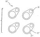
도 5는 패키지의 볼 랜딩의 저면도,5 is a bottom view of the ball landing of the package,
도 6은 볼 랜딩의 다른 실시예를 보인 도면,6 shows another embodiment of a ball landing,
도 7은 볼 랜딩의 또 다른 실시예를 보인 도면.7 shows another embodiment of a ball landing.
본 발명은 본딩 셀프(bonding shelf)상에 위치되어 있고 그리고 이 셀프의 에지를 따라 뻗어 있는 전도성 스트립에 의해 내부 전도성 전원/접지 플레인(plan- e)에 접속되어 있는 내부 본딩 패드를 가지고 있는 집적 회로 패키지이다. 상기 에지 스트립으로 인해, 종래 바이어는 상기 본딩 패드를 상기 플레인에 접속할 필요가 없으며, 이에따라 상기 패키지의 비용과 크기가 줄어든다. 상기 에지 스트립은 또한 상기 패키지의 전기적 성능을 개선시킨다. 상기 본딩 패드는 상기 패키지의 상부면에 부착된 열 슬러그(heat slug)에 장착되어 있는 집적 회로에 접속되어 있다. 상기 열 슬러그는 상기 집적 회로용의 접지 경로와 열 싱크(thermal sink)로서 기능할 수 있다. 상기 패키지는 상기 집적 회로에 제공된 신호의 전기 노이즈를 줄이기 위해 상기 패키지의 내부 경로에 접속되어 있는 커패시터를 가지고 있을 수도 있다. 또한, 상기 패키지는 상이한 전압 레벨 전용의 복수의 전원 플레인을 가지고 있을 수도 있다. 상기 본딩 패드와 상기 전도성 플레인은 상기 패키지의 바닥면에 위치되어 있는 랜딩 패드(landing pad)에 접속되어 있다. 상기 랜딩 패드에는 외부 인쇄 회로 기판에 납땜될 수 있는 땜납 볼이 부착되어 있다.The present invention is an integrated circuit having an internal bonding pad located on a bonding shelf and connected to an internal conductive power / ground plane by a conductive strip extending along the edge of the shelf. Package. The edge strip eliminates the need for conventional vias to connect the bonding pads to the plane, thereby reducing the cost and size of the package. The edge strip also improves the electrical performance of the package. The bonding pad is connected to an integrated circuit mounted on a heat slug attached to the top surface of the package. The heat slug may serve as a thermal sink and ground path for the integrated circuit. The package may have a capacitor connected to an internal path of the package to reduce electrical noise of a signal provided to the integrated circuit. The package may also have a plurality of power planes dedicated to different voltage levels. The bonding pad and the conductive plane are connected to a landing pad located at the bottom of the package. The landing pad is attached with solder balls that can be soldered to an external printed circuit board.
본 발명의 목적 및 이점은 이하의 상세한 설명과 첨부 도면을 검토하고 나면 당업자에게 쉽게 명백해진다.The objects and advantages of the present invention will become readily apparent to those skilled in the art upon reviewing the following detailed description and the accompanying drawings.
도면을 특히 참조 부호에 의해 참조하면, 도 1 내지 도 3에는 본 발명의 집적 회로 패키지 어셈블리(10)가 도시되어 있다. 이 어셈블리(10)는 패키지(14)내에 위치되어 있는 집적 회로(12)를 포함하고 있다. 이 집적 회로(12)는 마이크로프로세서와 같은 전자 장치일 수도 있다. 단일의 집적 회로(12)가 도시 및 설명되어 있지만, 복수의 집적 회로, 또는 기타 다른 IC 전자 장치가 본 발명의 패키지(14)내에 수용될 수 있음을 이해해야 한다.Referring to the drawings, in particular by reference numerals, FIGS. 1-3 show an integrated
상기 패키지(10)는 다층 인쇄 회로 기판(16)을 포함하고 있다. 이 인쇄 회로 기판(16)은 절연층(32-44)에 의해 분리된 복수의 전도층(18-28)을 가지고 있다. 상기 전도층(20,24,28)은 상기 패키지(10)의 내부 캐비티(48)내에 위치되어 있는 내부 본딩 패드(46)를 가지고 있다. 바람직한 실시예에서, 상기 다층 인쇄 회로 기판은 경질의 절연 기판(32,36,40,44)의 일측 또는 양측상에 전도성 라인/플레인을 가지고 있는 4개의 상이한 종래 인쇄 회로 기판으로 구성되어 있다. 상기 기판은 유리 충전된 에폭시 또는 기타 다른 종래 인쇄 회로 기판 재료일 수도 있다. 상기 인쇄 회로 기판들은 일반적으로 폴리이미드(34,38,42)와 같은 접착제로 함께 본딩되어 있다. 종래 인쇄 회로 기판 기술을 가지고 상기 패키지(10)를 구성하면, 상기 다층 패키지(10)의 개발 및 제조 비용이 줄어든다.The
상기 다층 인쇄 회로 기판(16)의 전도층은 전원과 디지탈 신호를 모두 전송할 수 있도록 구성되어 있으며, 이때 상기 디지탈 신호는 일반적으로 개별적인 리드(lead)에 의해 전달되고, 그리고 상기 전원은 전도성 플레인을 통해 공급된다. 바람직한 실시예에서, 전도층(18,26)은 접지(VSS) 전용이고, 전도층(20,22)은 전원(VCC)을 제공하며, 층(24,28)은 디지탈 신호를 전달한다. 각각의 전원층은 상이한 레벨의 전원을 제공할 수 있다. 예컨대, 상기 전도층(20)은 5 V 전원 공급기에 접속될 수 있고, 전도층(22)은 3.3 V 전원 공급기에 접속될 수 있다. 상기 집적 회로(12)는 이 회로(12)의 전원 요건에 따라 1개 또는 2개의 전원층(20,22)에 와이어 본딩될 수 있다.The conductive layer of the multilayer printed
도 4에 도시되어 있는 바와같이, 상기 본딩 패드(46)는 상기 패키지(10)의 층을 이룬 셀프상에 위치되어 있다. 상기 본딩 패드(46)들중 일부는 추가적인 스트립(52)을 가지고 있으며, 이때 이 스트립은 상기 절연 재료의 단부 주위를 둘러싸고 있고 그리고 아래에 있는 인접 전도층(22 또는 26)에 접속되어 있다. 구성 주위의 랩(wrap)은 어떠한 바이어를 사용하지 않고도 상기 본딩 패드(46)와 상기 전도성 플레인(22 또는 26) 사이에 상호 접속을 제공한다.As shown in FIG. 4, the
상기 인쇄 회로 기판(16)에는 열 슬러그(54)가 부착되어 있다. 이 열 슬러그(54)는 바람직하게는 열 및 전기 전도성이 있는 구리와 같은 재료로 구성된다. 상기 열 슬러그(54)는 전기 및 열 전도성의 접착제(30)로 전도층(18)에 장착될 수도 있다. 상기 열 슬러그(54)에는 인쇄 회로 기판(12)이 장착되어 있다. 상기 열 슬러그(54)에는 상기 집적 회로(12)의 바닥에 위치되어 있는 접지 패드가 전기 접속될 수 있다. 상기 열 슬러그(54)는 상기 패키지용 접지 플레인을 제공하고, 그리고 상기 집적 회로(12)를 상기 인쇄 회로 기판(16)에 전기 접속한다. 따라서, 상기 열 슬러그(54)는 접지 플레인과 열 싱크의 두가지 기능을 제공할 수 있다.The
상기 집적 회로(12)는 또한 와이어(56)에 의해 대응 내부 본딩 패드(46)에 접속되어 있는 외부 표면 패드(도시되지 않음)를 포함하고 있다. 상기 와이어(56)는 종래 와이어 본딩 기술에 의해 상기 집적 회로(12)와 상기 본딩 패드(46)에 부착될 수 있다. 상기 집적 회로(12)가 상기 인쇄 회로 기판(16)에 본딩된 후에, 상기 내부 캐비티(48)는 상기 회로(12)를 수용하고 있는 수용체(58)로 충전된다. 상기 인쇄 회로 기판(16)의 외부층을 절연시키기 위해서, 상기 패키지의 외부면에 땜납 마스크(60)가 제공되어 있다.The integrated
상기 인쇄 회로 기판(16)에는 커패시터와 같은 수동 소자(62)가 부착될 수 있다. 상기 접지 플레인(18)에 부착되어 있는 상기 커패시터(62)는 도금된 관통 구멍 바이어(64)에 의해 상기 전원 플레인에 접속되어 있다.The printed
도 3에 도시된 바와같이, 상기 인쇄 회로 기판(16)의 바닥층(44)은 복수의 랜딩 패드(70)에 부착된 복수의 땜납 볼(68)을 가지고 있다. 상기 랜딩 패드(70)는 상기 바이어와 상기 패키지(14)의 경로에 의해 상기 집적 회로(12)에 접속되어 있다. 도 1에 도시된 바와같이, 상기 땜납 볼(68)은 인쇄 회로 기판(72)에 부착되어 있다.As shown in FIG. 3, the
도 5 내지 도 7에는 다른 랜딩 패드(70,70',70'') 구조가 도시되어 있다. 회로 단락 및 환경 오염을 방지하기 위해서, 일반적으로 상기 패키지(14)의 바닥면을 가로질러 땜납 레지스트(60)가 제공되어 있다. 상기 땜납 볼(68)이 부착될 수 있도록 하기 위해, 상기 랜드(74,74',74'')상에는 개구(72,72',72'')가 각각 형성되어 있다. 상기 개구(72)는 도 5에 도시된 바와같이, 상기 랜드(74)보다 크도록 또는 도 7에 도시된 바와같이 상기 랜드(74'')보다 작도록 제조될 수 있다. 상기 랜드는 상기 패키지의 내부 경로에 상기 땜납 볼(68)을 접속하는 바이어(76)에 접속되어 있다.5 to 7 show
패키지(10)를 조립하기 위해, 개별적인 인쇄 회로 기판들이 접착제에 의해 함께 본딩되며, 이에따라 다층 인쇄 회로 기판(16)이 생성된다. 상기 개별적인 인쇄 회로 기판들은 종래 적층 기술을 이용하여 함께 본딩될 수 있다. 상기 인쇄 회로 기판들이 함께 본딩되기 전에, 상기 전도성 플레인과 트레이스(trace)가 원하는 패턴으로 에칭되며, 이에따라 전도층(18-28)이 생성된다. 상기 열 슬러그는 상기 인쇄 회로 기판(16)의 상부에 장착되어 있고, 상기 땜납 레지스트(60)는 상기 인쇄 회로 기판의 외부면에 제공되어 있다.To assemble the
다층 기판(16)과 열 슬러그(54)가 조립된 후에, 상기 땜납 볼(68)이 상기 랜딩 패드(70)에 부착될 수 있다. 상기 패키지는 일반적으로 집적 회로(12)의 다음의 용도를 위해 별개의 유닛으로서 적재된다. 상기 집적 회로(12)는 열 슬러그(58)에 장착되어 있고, 와이어는 상기 인쇄 회로 기판(16)에 본딩되어 있다. 다음에, 상기 패키지는 테스트되고, 그리고 상기 집적 회로(12)를 수용하기 위해 수용체(56)로 충전될 수도 있다.After the
특정 실시예에 대해서 설명되고 첨부 도면에 도시되어 있지만, 이러한 실시예는 넓은 본 발명의 예시에 불과하지 이에 한정되는 것은 아니며, 그리고 본 발명은 기타 다른 각종 변형예가 당업자에게 행해질 수 있으므로 도시 및 설명된 상기 특정 구성 및 배열에 한정되지 않음을 이해해야 한다.Although specific embodiments have been described and shown in the accompanying drawings, these embodiments are merely illustrative of the broad invention and should not be construed as limiting, and the invention is not limited to the scope of the invention. It should be understood that the present invention is not limited to the above specific configuration and arrangement.
Claims (17)
Translated fromKoreanApplications Claiming Priority (3)
| Application Number | Priority Date | Filing Date | Title |
|---|---|---|---|
| US8/399,162 | 1995-03-02 | ||
| US08/399,162US5557502A (en) | 1995-03-02 | 1995-03-02 | Structure of a thermally and electrically enhanced plastic ball grid array package |
| PCT/US1996/002000WO1996027280A1 (en) | 1995-03-02 | 1996-02-15 | Thermally and electrically enhanced ball grid package |
Publications (2)
| Publication Number | Publication Date |
|---|---|
| KR19980702622A KR19980702622A (en) | 1998-08-05 |
| KR100281813B1true KR100281813B1 (en) | 2001-02-15 |
Family
ID=23578410
Family Applications (1)
| Application Number | Title | Priority Date | Filing Date |
|---|---|---|---|
| KR1019970706027AExpired - Fee RelatedKR100281813B1 (en) | 1995-03-02 | 1996-02-15 | Thermally and electrically enhanced ball grid package |
Country Status (8)
| Country | Link |
|---|---|
| US (1) | US5557502A (en) |
| JP (1) | JPH11501157A (en) |
| KR (1) | KR100281813B1 (en) |
| AU (1) | AU4924196A (en) |
| GB (1) | GB2314458B (en) |
| MY (1) | MY119410A (en) |
| TW (1) | TW363335B (en) |
| WO (1) | WO1996027280A1 (en) |
Families Citing this family (72)
| Publication number | Priority date | Publication date | Assignee | Title |
|---|---|---|---|---|
| JP2636777B2 (en)* | 1995-02-14 | 1997-07-30 | 日本電気株式会社 | Semiconductor module for microprocessor |
| US6388203B1 (en) | 1995-04-04 | 2002-05-14 | Unitive International Limited | Controlled-shaped solder reservoirs for increasing the volume of solder bumps, and structures formed thereby |
| ATE240586T1 (en) | 1995-04-05 | 2003-05-15 | Unitive Int Ltd | A SOLDER BUMP STRUCTURE FOR A MICROELECTRONIC SUBSTRATE |
| GB9515651D0 (en)* | 1995-07-31 | 1995-09-27 | Sgs Thomson Microelectronics | A method of manufacturing a ball grid array package |
| US5767623A (en)* | 1995-09-11 | 1998-06-16 | Planar Systems, Inc. | Interconnection between an active matrix electroluminescent display and an electrical cable |
| US5784262A (en)* | 1995-11-06 | 1998-07-21 | Symbios, Inc. | Arrangement of pads and through-holes for semiconductor packages |
| US5796589A (en)* | 1995-12-20 | 1998-08-18 | Intel Corporation | Ball grid array integrated circuit package that has vias located within the solder pads of a package |
| CN1098023C (en) | 1996-01-11 | 2003-01-01 | 揖斐电株式会社 | Printed circuit board and manufacture thereof |
| US6256189B1 (en)* | 1996-03-29 | 2001-07-03 | Intel Corporation | Heat slug design which facilitates mounting of discrete components on a package without losing lands or pins in the package |
| US6043559A (en) | 1996-09-09 | 2000-03-28 | Intel Corporation | Integrated circuit package which contains two in plane voltage busses and a wrap around conductive strip that connects a bond finger to one of the busses |
| US5787575A (en)* | 1996-09-09 | 1998-08-04 | Intel Corporation | Method for plating a bond finger of an intergrated circuit package |
| US6031283A (en)* | 1996-09-09 | 2000-02-29 | Intel Corporation | Integrated circuit package |
| US5804771A (en) | 1996-09-26 | 1998-09-08 | Intel Corporation | Organic substrate (PCB) slip plane "stress deflector" for flip chip deivces |
| US6167948B1 (en) | 1996-11-18 | 2001-01-02 | Novel Concepts, Inc. | Thin, planar heat spreader |
| US5796169A (en)* | 1996-11-19 | 1998-08-18 | International Business Machines Corporation | Structurally reinforced ball grid array semiconductor package and systems |
| US5847935A (en)* | 1996-12-16 | 1998-12-08 | Sarnoff Corporation | Electronic circuit chip package |
| JP3382482B2 (en)* | 1996-12-17 | 2003-03-04 | 新光電気工業株式会社 | Method of manufacturing circuit board for semiconductor package |
| US6069793A (en)* | 1997-01-24 | 2000-05-30 | Hitachi, Ltd. | Circuit module and information processing apparatus |
| US5990421A (en)* | 1997-02-18 | 1999-11-23 | Intel Corporation | Built in board resistors |
| US6175161B1 (en)* | 1998-05-22 | 2001-01-16 | Alpine Microsystems, Inc. | System and method for packaging integrated circuits |
| US6107683A (en)* | 1997-06-20 | 2000-08-22 | Substrate Technologies Incorporated | Sequentially built integrated circuit package |
| US5982633A (en)* | 1997-08-20 | 1999-11-09 | Compaq Computer Corporation | Opposed ball grid array mounting |
| US6169664B1 (en)* | 1998-01-05 | 2001-01-02 | Texas Instruments Incorporated | Selective performance enhancements for interconnect conducting paths |
| US6310303B1 (en)* | 1998-03-10 | 2001-10-30 | John J. Luvara | Structure for printed circuit design |
| US5963023A (en)* | 1998-03-21 | 1999-10-05 | Advanced Micro Devices, Inc. | Power surge management for high performance integrated circuit |
| US6828666B1 (en) | 1998-03-21 | 2004-12-07 | Advanced Micro Devices, Inc. | Low inductance power distribution system for an integrated circuit chip |
| US6720501B1 (en) | 1998-04-14 | 2004-04-13 | Formfactor, Inc. | PC board having clustered blind vias |
| US6060777A (en) | 1998-07-21 | 2000-05-09 | Intel Corporation | Underside heat slug for ball grid array packages |
| US5977863A (en)* | 1998-08-10 | 1999-11-02 | Cts Corporation | Low cross talk ball grid array resistor network |
| US6326677B1 (en) | 1998-09-04 | 2001-12-04 | Cts Corporation | Ball grid array resistor network |
| US7020958B1 (en) | 1998-09-15 | 2006-04-04 | Intel Corporation | Methods forming an integrated circuit package with a split cavity wall |
| US6153829A (en)* | 1998-09-15 | 2000-11-28 | Intel Corporation | Split cavity wall plating for an integrated circuit package |
| US6618267B1 (en) | 1998-09-22 | 2003-09-09 | International Business Machines Corporation | Multi-level electronic package and method for making same |
| US6084779A (en)* | 1998-10-02 | 2000-07-04 | Sigrity, Inc. | Ground and power patches on printed circuit board signal planes in the areas of integrated circuit chips |
| US6097277A (en)* | 1998-11-05 | 2000-08-01 | Cts | Resistor network with solder sphere connector |
| US6005777A (en)* | 1998-11-10 | 1999-12-21 | Cts Corporation | Ball grid array capacitor |
| US6354850B1 (en) | 1998-12-15 | 2002-03-12 | Fci Americas Technology, Inc. | Electrical connector with feature for limiting the effects of coefficient of thermal expansion differential |
| US6288906B1 (en)* | 1998-12-18 | 2001-09-11 | Intel Corporation | Multiple layer printed circuit board having power planes on outer layers |
| US6191479B1 (en) | 1999-02-13 | 2001-02-20 | Advanced Micro Devices, Inc. | Decoupling capacitor configuration for integrated circuit chip |
| US6194979B1 (en) | 1999-03-18 | 2001-02-27 | Cts Corporation | Ball grid array R-C network with high density |
| US6429383B1 (en) | 1999-04-14 | 2002-08-06 | Intel Corporation | Apparatus and method for improving circuit board solder |
| JP3368870B2 (en)* | 1999-06-25 | 2003-01-20 | 日本電気株式会社 | Package substrate and semiconductor device having the same |
| US6288344B1 (en)* | 1999-08-20 | 2001-09-11 | Cardiac Pacemakers, Inc. | Integrated EMI shield utilizing a hybrid edge |
| US6274474B1 (en)* | 1999-10-25 | 2001-08-14 | International Business Machines Corporation | Method of forming BGA interconnections having mixed solder profiles |
| US6246312B1 (en) | 2000-07-20 | 2001-06-12 | Cts Corporation | Ball grid array resistor terminator network |
| US6577508B1 (en) | 2000-08-10 | 2003-06-10 | Nortel Networks Limited | Multilayer circuit board |
| DE60108413T2 (en) | 2000-11-10 | 2005-06-02 | Unitive Electronics, Inc. | METHOD FOR POSITIONING COMPONENTS WITH THE HELP OF LIQUID DRIVES AND STRUCTURES THEREFOR |
| US6580619B2 (en)* | 2000-11-30 | 2003-06-17 | Intel Corporation | Multilayer reference plane in package devices |
| US6628528B2 (en)* | 2000-11-30 | 2003-09-30 | Theodore Zale Schoenborn | Current sharing in memory packages |
| US6863209B2 (en) | 2000-12-15 | 2005-03-08 | Unitivie International Limited | Low temperature methods of bonding components |
| US6743127B2 (en)* | 2002-04-02 | 2004-06-01 | Wilson Sporting Goods Co. | Bat with composite handle |
| US7531898B2 (en) | 2002-06-25 | 2009-05-12 | Unitive International Limited | Non-Circular via holes for bumping pads and related structures |
| WO2004001837A2 (en) | 2002-06-25 | 2003-12-31 | Unitive International Limited | Methods of forming electronic structures including conductive shunt layers and related structures |
| US7547623B2 (en) | 2002-06-25 | 2009-06-16 | Unitive International Limited | Methods of forming lead free solder bumps |
| US6813154B2 (en)* | 2002-12-10 | 2004-11-02 | Motorola, Inc. | Reversible heat sink packaging assembly for an integrated circuit |
| TWI225899B (en) | 2003-02-18 | 2005-01-01 | Unitive Semiconductor Taiwan C | Etching solution and method for manufacturing conductive bump using the etching solution to selectively remove barrier layer |
| US20040227233A1 (en)* | 2003-05-16 | 2004-11-18 | Nokia Corporation | Interconnection pattern design |
| US7180186B2 (en)* | 2003-07-31 | 2007-02-20 | Cts Corporation | Ball grid array package |
| US6946733B2 (en)* | 2003-08-13 | 2005-09-20 | Cts Corporation | Ball grid array package having testing capability after mounting |
| US7049216B2 (en)* | 2003-10-14 | 2006-05-23 | Unitive International Limited | Methods of providing solder structures for out plane connections |
| US7057115B2 (en) | 2004-01-26 | 2006-06-06 | Litton Systems, Inc. | Multilayered circuit board for high-speed, differential signals |
| TW200603698A (en) | 2004-04-13 | 2006-01-16 | Unitive International Ltd | Methods of forming solder bumps on exposed metal pads and related structures |
| JP4211986B2 (en)* | 2004-12-02 | 2009-01-21 | パナソニック株式会社 | Printed circuit board and printed circuit board design method, IC package connection terminal design method, and IC package connection method |
| US7243983B2 (en)* | 2005-02-23 | 2007-07-17 | Asc Incorporated | Retractable pillar for convertible vehicle |
| FR2888975B1 (en)* | 2005-07-21 | 2007-09-07 | Atmel Corp | SECURITY METHOD FOR DATA PROTECTION |
| US7932615B2 (en) | 2006-02-08 | 2011-04-26 | Amkor Technology, Inc. | Electronic devices including solder bumps on compliant dielectric layers |
| US7674701B2 (en) | 2006-02-08 | 2010-03-09 | Amkor Technology, Inc. | Methods of forming metal layers using multi-layer lift-off patterns |
| DE102006018161A1 (en)* | 2006-04-19 | 2007-10-25 | Patent-Treuhand-Gesellschaft für elektrische Glühlampen mbH | Electronic component module |
| US8354743B2 (en)* | 2010-01-27 | 2013-01-15 | Honeywell International Inc. | Multi-tiered integrated circuit package |
| TWI489922B (en)* | 2013-07-15 | 2015-06-21 | Mpi Corp | Multilayer circuit boards |
| US9741644B2 (en) | 2015-05-04 | 2017-08-22 | Honeywell International Inc. | Stacking arrangement for integration of multiple integrated circuits |
| US11640934B2 (en)* | 2018-03-30 | 2023-05-02 | Intel Corporation | Lithographically defined vertical interconnect access (VIA) in dielectric pockets in a package substrate |
Citations (1)
| Publication number | Priority date | Publication date | Assignee | Title |
|---|---|---|---|---|
| US5219062A (en)* | 1990-03-02 | 1993-06-15 | Hans Oetiker Ag Maschinen- Und Apparatefabrik | Conveyor arrangement for loose material, especially blasting materials for sand-blasting installations |
Family Cites Families (10)
| Publication number | Priority date | Publication date | Assignee | Title |
|---|---|---|---|---|
| US4420767A (en)* | 1978-11-09 | 1983-12-13 | Zilog, Inc. | Thermally balanced leadless microelectronic circuit chip carrier |
| US4819041A (en)* | 1983-12-30 | 1989-04-04 | Amp Incorporated | Surface mounted integrated circuit chip package and method for making same |
| US4899118A (en)* | 1988-12-27 | 1990-02-06 | Hughes Aircraft Company | Low temperature cofired ceramic packages for microwave and millimeter wave gallium arsenide integrated circuits |
| US5218515A (en)* | 1992-03-13 | 1993-06-08 | The United States Of America As Represented By The United States Department Of Energy | Microchannel cooling of face down bonded chips |
| US5285352A (en)* | 1992-07-15 | 1994-02-08 | Motorola, Inc. | Pad array semiconductor device with thermal conductor and process for making the same |
| US5291062A (en)* | 1993-03-01 | 1994-03-01 | Motorola, Inc. | Area array semiconductor device having a lid with functional contacts |
| US5355283A (en)* | 1993-04-14 | 1994-10-11 | Amkor Electronics, Inc. | Ball grid array with via interconnection |
| US5357672A (en)* | 1993-08-13 | 1994-10-25 | Lsi Logic Corporation | Method and system for fabricating IC packages from laminated boards and heat spreader |
| US5442852A (en)* | 1993-10-26 | 1995-08-22 | Pacific Microelectronics Corporation | Method of fabricating solder ball array |
| US5400220A (en)* | 1994-05-18 | 1995-03-21 | Dell Usa, L.P. | Mechanical printed circuit board and ball grid array interconnect apparatus |
- 1995
- 1995-03-02USUS08/399,162patent/US5557502A/ennot_activeExpired - Lifetime
- 1996
- 1996-02-14MYMYPI96000570Apatent/MY119410A/enunknown
- 1996-02-15JPJP8526277Apatent/JPH11501157A/enactivePending
- 1996-02-15WOPCT/US1996/002000patent/WO1996027280A1/enactiveIP Right Grant
- 1996-02-15KRKR1019970706027Apatent/KR100281813B1/ennot_activeExpired - Fee Related
- 1996-02-15GBGB9717189Apatent/GB2314458B/ennot_activeExpired - Fee Related
- 1996-02-15AUAU49241/96Apatent/AU4924196A/ennot_activeAbandoned
- 1996-03-21TWTW085103412Apatent/TW363335B/ennot_activeIP Right Cessation
Patent Citations (1)
| Publication number | Priority date | Publication date | Assignee | Title |
|---|---|---|---|---|
| US5219062A (en)* | 1990-03-02 | 1993-06-15 | Hans Oetiker Ag Maschinen- Und Apparatefabrik | Conveyor arrangement for loose material, especially blasting materials for sand-blasting installations |
Also Published As
| Publication number | Publication date |
|---|---|
| US5557502A (en) | 1996-09-17 |
| GB2314458A (en) | 1997-12-24 |
| WO1996027280A1 (en) | 1996-09-06 |
| GB2314458B (en) | 1999-01-06 |
| GB9717189D0 (en) | 1997-10-22 |
| KR19980702622A (en) | 1998-08-05 |
| JPH11501157A (en) | 1999-01-26 |
| MY119410A (en) | 2005-05-31 |
| AU4924196A (en) | 1996-09-18 |
| TW363335B (en) | 1999-07-01 |
Similar Documents
| Publication | Publication Date | Title |
|---|---|---|
| KR100281813B1 (en) | Thermally and electrically enhanced ball grid package | |
| US6043559A (en) | Integrated circuit package which contains two in plane voltage busses and a wrap around conductive strip that connects a bond finger to one of the busses | |
| US6218731B1 (en) | Tiny ball grid array package | |
| US5825628A (en) | Electronic package with enhanced pad design | |
| US5625166A (en) | Structure of a thermally and electrically enhanced plastic pin grid array (PPGA) package for high performance devices with wire bond interconnect | |
| US6888240B2 (en) | High performance, low cost microelectronic circuit package with interposer | |
| US6060777A (en) | Underside heat slug for ball grid array packages | |
| CN100355064C (en) | Low cost microelectronic circuit package | |
| US20060131716A1 (en) | Stacking system and method | |
| US20080067662A1 (en) | Modularized Die Stacking System and Method | |
| JPH09283695A (en) | Semiconductor mounting structure | |
| WO1996013854A9 (en) | Thermally and electrically enhanced plastic pin grid array (ppga) package | |
| US5787575A (en) | Method for plating a bond finger of an intergrated circuit package | |
| US20060097370A1 (en) | Stepped integrated circuit packaging and mounting | |
| US5473190A (en) | Tab tape | |
| JPH0477469B2 (en) | ||
| US6340839B1 (en) | Hybrid integrated circuit | |
| US6153829A (en) | Split cavity wall plating for an integrated circuit package | |
| US7057116B2 (en) | Selective reference plane bridge(s) on folded package | |
| US6031283A (en) | Integrated circuit package | |
| US5691569A (en) | Integrated circuit package that has a plurality of staggered pins | |
| JPS616846A (en) | Plug-in package with capacitor | |
| EP0521720A1 (en) | Heat-dissipating multi-layer circuit board | |
| US20020063331A1 (en) | Film carrier semiconductor device | |
| US6570271B2 (en) | Apparatus for routing signals |
Legal Events
| Date | Code | Title | Description |
|---|---|---|---|
| A201 | Request for examination | ||
| PA0105 | International application | St.27 status event code:A-0-1-A10-A15-nap-PA0105 | |
| PA0201 | Request for examination | St.27 status event code:A-1-2-D10-D11-exm-PA0201 | |
| R17-X000 | Change to representative recorded | St.27 status event code:A-3-3-R10-R17-oth-X000 | |
| PG1501 | Laying open of application | St.27 status event code:A-1-1-Q10-Q12-nap-PG1501 | |
| R17-X000 | Change to representative recorded | St.27 status event code:A-3-3-R10-R17-oth-X000 | |
| E902 | Notification of reason for refusal | ||
| PE0902 | Notice of grounds for rejection | St.27 status event code:A-1-2-D10-D21-exm-PE0902 | |
| P11-X000 | Amendment of application requested | St.27 status event code:A-2-2-P10-P11-nap-X000 | |
| P13-X000 | Application amended | St.27 status event code:A-2-2-P10-P13-nap-X000 | |
| E701 | Decision to grant or registration of patent right | ||
| PE0701 | Decision of registration | St.27 status event code:A-1-2-D10-D22-exm-PE0701 | |
| GRNT | Written decision to grant | ||
| PR0701 | Registration of establishment | St.27 status event code:A-2-4-F10-F11-exm-PR0701 | |
| PR1002 | Payment of registration fee | St.27 status event code:A-2-2-U10-U12-oth-PR1002 Fee payment year number:1 | |
| PG1601 | Publication of registration | St.27 status event code:A-4-4-Q10-Q13-nap-PG1601 | |
| PR1001 | Payment of annual fee | St.27 status event code:A-4-4-U10-U11-oth-PR1001 Fee payment year number:4 | |
| R18-X000 | Changes to party contact information recorded | St.27 status event code:A-5-5-R10-R18-oth-X000 | |
| PR1001 | Payment of annual fee | St.27 status event code:A-4-4-U10-U11-oth-PR1001 Fee payment year number:5 | |
| PR1001 | Payment of annual fee | St.27 status event code:A-4-4-U10-U11-oth-PR1001 Fee payment year number:6 | |
| PR1001 | Payment of annual fee | St.27 status event code:A-4-4-U10-U11-oth-PR1001 Fee payment year number:7 | |
| L13-X000 | Limitation or reissue of ip right requested | St.27 status event code:A-2-3-L10-L13-lim-X000 | |
| U15-X000 | Partial renewal or maintenance fee paid modifying the ip right scope | St.27 status event code:A-4-4-U10-U15-oth-X000 | |
| PR1001 | Payment of annual fee | St.27 status event code:A-4-4-U10-U11-oth-PR1001 Fee payment year number:8 | |
| PR1001 | Payment of annual fee | St.27 status event code:A-4-4-U10-U11-oth-PR1001 Fee payment year number:9 | |
| FPAY | Annual fee payment | Payment date:20091118 Year of fee payment:10 | |
| PR1001 | Payment of annual fee | St.27 status event code:A-4-4-U10-U11-oth-PR1001 Fee payment year number:10 | |
| LAPS | Lapse due to unpaid annual fee | ||
| PC1903 | Unpaid annual fee | St.27 status event code:A-4-4-U10-U13-oth-PC1903 Not in force date:20101122 Payment event data comment text:Termination Category : DEFAULT_OF_REGISTRATION_FEE | |
| PC1903 | Unpaid annual fee | St.27 status event code:N-4-6-H10-H13-oth-PC1903 Ip right cessation event data comment text:Termination Category : DEFAULT_OF_REGISTRATION_FEE Not in force date:20101122 | |
| R18-X000 | Changes to party contact information recorded | St.27 status event code:A-5-5-R10-R18-oth-X000 | |
| R18-X000 | Changes to party contact information recorded | St.27 status event code:A-5-5-R10-R18-oth-X000 | |
| R18-X000 | Changes to party contact information recorded | St.27 status event code:A-5-5-R10-R18-oth-X000 | |
| R18-X000 | Changes to party contact information recorded | St.27 status event code:A-5-5-R10-R18-oth-X000 | |
| P22-X000 | Classification modified | St.27 status event code:A-4-4-P10-P22-nap-X000 |