KR100280637B1 - Computer system capable of data update of fixed flash ROM and its control method - Google Patents
Computer system capable of data update of fixed flash ROM and its control methodDownload PDFInfo
- Publication number
- KR100280637B1 KR100280637B1KR1019970062326AKR19970062326AKR100280637B1KR 100280637 B1KR100280637 B1KR 100280637B1KR 1019970062326 AKR1019970062326 AKR 1019970062326AKR 19970062326 AKR19970062326 AKR 19970062326AKR 100280637 B1KR100280637 B1KR 100280637B1
- Authority
- KR
- South Korea
- Prior art keywords
- flash rom
- data
- original
- computer system
- flash
- Prior art date
- Legal status (The legal status is an assumption and is not a legal conclusion. Google has not performed a legal analysis and makes no representation as to the accuracy of the status listed.)
- Expired - Fee Related
Links
Images


Classifications
- G—PHYSICS
- G06—COMPUTING OR CALCULATING; COUNTING
- G06F—ELECTRIC DIGITAL DATA PROCESSING
- G06F12/00—Accessing, addressing or allocating within memory systems or architectures
- G—PHYSICS
- G11—INFORMATION STORAGE
- G11C—STATIC STORES
- G11C16/00—Erasable programmable read-only memories
- G11C16/02—Erasable programmable read-only memories electrically programmable
- G11C16/06—Auxiliary circuits, e.g. for writing into memory
- G11C16/10—Programming or data input circuits
- G11C16/102—External programming circuits, e.g. EPROM programmers; In-circuit programming or reprogramming; EPROM emulators
- G11C16/105—Circuits or methods for updating contents of nonvolatile memory, especially with 'security' features to ensure reliable replacement, i.e. preventing that old data is lost before new data is reliably written
- G—PHYSICS
- G06—COMPUTING OR CALCULATING; COUNTING
- G06F—ELECTRIC DIGITAL DATA PROCESSING
- G06F8/00—Arrangements for software engineering
- G06F8/60—Software deployment
- G06F8/65—Updates
- G—PHYSICS
- G11—INFORMATION STORAGE
- G11C—STATIC STORES
- G11C16/00—Erasable programmable read-only memories
- G11C16/02—Erasable programmable read-only memories electrically programmable
- G11C16/06—Auxiliary circuits, e.g. for writing into memory
- G11C16/10—Programming or data input circuits
- G11C16/102—External programming circuits, e.g. EPROM programmers; In-circuit programming or reprogramming; EPROM emulators
Landscapes
- Engineering & Computer Science (AREA)
- Theoretical Computer Science (AREA)
- General Engineering & Computer Science (AREA)
- Computer Security & Cryptography (AREA)
- Software Systems (AREA)
- Physics & Mathematics (AREA)
- General Physics & Mathematics (AREA)
- Stored Programmes (AREA)
- Read Only Memory (AREA)
Abstract
Translated fromKoreanDescription
Translated fromKorean이 발명은 고정된 플래시 롬(Flash ROM:Read Only Memory)의 데이터(data) 갱신이 가능한 컴퓨터 시스템(computer system) 및 그 제어 방법에 관한 것으로서, 더욱 상세하게 말하자면 컴퓨터 시스템 내의 인쇄회로기판(Printed Circuit Board: 이하 PCB라고 함)에 고정되어 있는 플래시 롬을 PCB로부터 분리하지 않고 데이터를 갱신할 수 있는 컴퓨터 시스템 및 그 제어 방법에 관한 것이다.BACKGROUND OF THE
일반적으로, 플래시 롬은 갱신 가능한 검색 전용 메모리인 프로그래머블 롬(PROM:Programmable ROM) 중에서 전기적으로 이전의 내용을 없애고, 새로이 고쳐 쓰게 하는 칩을 말하며, 플래시 EEPROM(Electrically Erasable PROM)이라고도 부른다.In general, a flash ROM refers to a chip that electrically erases and rewrites previous contents of a programmable ROM (PROM: Programmable ROM), which is an updateable search-only memory.
같은 기능을 가진 것으로 EEPROM이 있지만, 플래시 롬 쪽이 구조가 간단하고, 칩(chip)을 작게 만들 수 있기 때문에 DRAM(Dynamic Random Access Memory) 보다 싸게 제조할 수 있다. 주로 휴대용 컴퓨터의 대용량 기억 장치에 이용되고 있으며, 하드 디스크 드라이브(hard disk drive)에 비해 유리한 점으로는 소형화할 수 있다는 것이고, 백업(backup) 전원이 필요없으며, 충격에도 강하다.The EEPROM has the same function, but the flash ROM can be manufactured cheaper than the DRAM (Dynamic Random Access Memory) because the structure is simple and the chip can be made small. It is mainly used in the mass storage device of a portable computer, and it can be miniaturized in an advantage over a hard disk drive, does not need a backup power source, and is strong in shock.
그러나, 현재는 부분적으로 소거할 수 있는 영역이 너무 크고, 갱신 가능한 횟수가 1만회 정도로 적다는 결점도 있다.However, there is a drawback that the area which can be partially erased is too large and the number of times that can be updated is as small as 10,000 times.
도 1은 종래의 플래시 롬 라이터(writer)가 결합되어 있는 컴퓨터 시스템의 구성도이다.1 is a block diagram of a computer system in which a conventional flash ROM writer is incorporated.
도 1에 도시되어 있듯이, 종래의 플래시 롬 라이터가 결합되어 있는 컴퓨터 시스템은 컴퓨터 본체(1), 모니터(2), 키보드(3), 그리고 롬 라이터(4)로 이루어져 있다.As shown in FIG. 1, a computer system in which a conventional flash ROM writer is coupled is composed of a computer
롬 라이터(4)는 케이블(7)을 통해 컴퓨터 본체(1)에 연결되며, 롬 탑재부(5)에 플래시 롬을 삽입하여 사용하는 것을 도시하고 있다.The ROM writer 4 is connected to the computer
그리고, 사용자는 유틸리티 프로그램(utility program)에 의해 플래시 롬 데이터의 소거, 읽기, 쓰기 및 확인 작업을 하게 된다.In addition, the user may erase, read, write, and verify flash ROM data by a utility program.
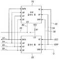
도 2는 일반적인 플래시 롬의 외형도로서, PCB(9) 상에 탑재되어 있는 것을 도시하고 있으며, 현재 컴퓨터 시스템 및 제어 장치 등에 사용되는 플래시 롬(8)은 표면실장 디바이스(SMD:Surface Mounted Device)로 제작되고, 원가 측면을 고려하여 소켓(socket) 등을 사용하지 않고 대부분이 PCB(9) 상에 직접 실장되고 있다.FIG. 2 is an external view of a general flash ROM, which is mounted on a
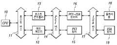
도 3은 일반적인 컴퓨터 시스템의 블록도이다.3 is a block diagram of a typical computer system.
도 3에 도시되어 있듯이, 일반적인 컴퓨터 시스템은 전체적인 제어를 수행하는 중앙처리장치(CPU:Central Processing Unit, 10)와; 데이터, 명령 그리고 제어 신호의 통로가 되는 호스트 버스(host bus, 11), PCI 버스(14) 그리고 ISA 버스(17)와; 호스트 버스(11)에 연결되고 중앙처리장치(10)가 시스템 소프트웨어(software) 및 사용자 소프트웨어를 로드(load)시킬 장소를 제공하는 기억 장치인 메인(main) 메모리(12)와; 호스트 버스(11)와 PCI 버스(14) 사이를 연결하는 호스트 콘트롤러(13)와; PCI 버스(14)에 연결되는 PCI 장치915)와; PCI 버스와 ISA 버스(17) 사이를 연결하는 PCI-ISA 브리지(bridge)와; 중앙처리장치(10)가 실행시킬 특정 프로그램이 탑재되어 있는 기억 장치인 플래시 롬(18)과; ISA 버스(17)에 연결되어 있는 ISA 장치(19)를 포함한다.As shown in Fig. 3, a general computer system includes a central processing unit (CPU) 10 for performing overall control; A
도 4는 일반적인 컴퓨터 시스템의 플래시 롬 데이터 갱신 방법의 순서도이다.4 is a flowchart of a flash ROM data updating method of a general computer system.
도 4에 도시되어 있듯이, 일반적인 컴퓨터 시스템의 전원이 온(on)되면(S1), 중앙처리장치(10)는 플래시 롬(18)에 탑재되어 있는 롬 데이터를 읽어서 기본 동작을 검사한다(S2, S3).As shown in FIG. 4, when the power of a general computer system is turned on (S1), the
이 때, 플래시 롬(18) 내에 탑재되어 있는 데이터가 지워지거나 깨져 있다면 시스템은 더 이상 동작하지 않거나 오동작을 하게 된다.At this time, if the data mounted in the
만약, 이상없이 기본 동작이 수행되면 OS(Operating System)가 실행되어(S4) 사용자 환경이 되고, 플래시 롬(18) 데이터 갱신 작업을 하기 위해(S5) 플래시 롬(18) 유틸리티 프로그램을 사용하여 원본 롬 데이터를 읽는다(S6). 다음에, 원본 롬 데이터를 이용하여 플래시 롬(18) 데이터를 갱신한다(S7). 한편, 상기 단계(S5)에서 플래시 롬(18) 데이터 갱신 작업을 하지 않으면 계속 사용자 환경 상태로 있다(S8).If the basic operation is performed without any abnormality, the OS (Operating System) is executed (S4) to become the user environment, and the flash ROM (18) is used to update the data (S5) using the flash ROM (18) utility program. Read the ROM data (S6). Next, the
여기에서, 플래시 롬(18) 데이터 갱신 중에 컴퓨터 시스템에 이상이 발생하면 플래시 롬(18)의 데이터가 깨져서, 컴퓨터 시스템의 전원을 다시 온시키면 시스템이 작동이 되지 않게 된다.Here, if an abnormality occurs in the computer system during the update of the
이와 같이, 컴퓨터 시스템의 PCB(9)에 고정되어 있는 플래시 롬(8, 18)의 데이터가 지워졌거나 깨졌을 경우에는 PCB(9)로부터 플래시 롬(8, 18)을 빼내어 도 1에 도시한 롬 라이터(4) 장비를 이용하여 플래시 롬(8, 18) 데이터를 갱신한 후, 다시 PCB(9)에 장착시켜서 사용하여야 한다.As described above, when data of the
종래에는 PCB에 플래시 롬이 실장되어 있는 경우에, 플래시 롬의 데이터가 잘못되었거나 소프트웨어의 업그레이드(upgrade) 등 상기 플래시 롬에 새로운 데이터를 써넣어야 할 때, 인두 등을 이용하여 플래시 롬을 PCB에서 분리한 후, 플래시 롬 라이터로 새로운 데이터를 써넣은 플래시 롬을 PCB에 재실장하여야 하기 때문에 사용이 불편하며, 또한 인두 등의 고열을 발생하는 장비를 사용하기 때문에 PCB 패턴(pattern) 등을 손상시킬 수 있다는 문제점이 있다.Conventionally, when a flash ROM is mounted on a PCB, when the data of the flash ROM is wrong or when new data is to be written to the flash ROM such as software upgrade, the flash ROM is separated from the PCB by using a soldering iron or the like. After that, it is inconvenient to use the flash ROM, which writes new data with the flash ROM writer, on the PCB, and it can damage the PCB pattern because it uses equipment that generates high temperature such as iron. There is a problem.
따라서, 이 발명의 목적은 상기한 종래의 문제점을 해결하기 위한 것으로서, 컴퓨터 시스템 및 제어 장치의 PCB에서 플래시 롬을 분리시키지 않고, PCB에 플래시 롬이 실장된 상태에서 직접 데이터를 갱신함으로써, 시간적, 인적 낭비를 줄이고, PCB 등에 가해질 물리적인 손상을 방지할 수 있는 고정된 플래시 롬 데이터의 갱신이 가능한 컴퓨터 시스템 및 그 제어 방법을 제공하는 데 있다.Accordingly, an object of the present invention is to solve the above-described problems, and by updating data directly in a state where the flash ROM is mounted on the PCB, without separating the flash ROM from the PCB of the computer system and the control device, The present invention provides a computer system capable of updating fixed flash ROM data that can reduce human waste and prevent physical damage to a PCB, and a control method thereof.
도 1은 종래의 플래시 롬 라이터가 결합되어 있는 컴퓨터 시스템의 구성도이고,1 is a configuration diagram of a computer system in which a conventional flash ROM writer is coupled,
도 2는 종래의 기술에 따른 플래시 롬의 외형도이고,2 is an external view of a flash ROM according to the prior art,
도 3은 일반적인 컴퓨터 시스템의 블록도이고,3 is a block diagram of a typical computer system,
도 4는 일반적인 컴퓨터 시스템의 플래시 롬 데이터 갱신 방법의 순서도이고,4 is a flowchart of a flash ROM data updating method of a general computer system;
도 5는 이 발명의 실시예에 따른 고정된 플래시 롬의 데이터 갱신이 가능한 컴퓨터 시스템에서 원본 플래시 롬이 장착되기 전의 회로도이고,5 is a circuit diagram before an original flash ROM is mounted in a computer system capable of updating data of a fixed flash ROM according to an embodiment of the present invention.
도 6은 이 발명의 실시예에 따른 고정된 플래시 롬의 데이터 갱신이 가능한 컴퓨터 시스템에서 원본 플래시 롬이 장착되기 전의 메인 보드를 도시한 도면이고,6 is a diagram illustrating a main board before an original flash ROM is mounted in a computer system capable of updating data of a fixed flash ROM according to an embodiment of the present invention.
도 7은 이 발명의 실시예에 따른 고정된 플래시 롬의 데이터 갱신이 가능한 컴퓨터 시스템에서 원본 플래시 롬을 메인 보드 상에 장착하기 위한 연결을 도시한 도면이고,7 is a diagram illustrating a connection for mounting an original flash ROM on a main board in a computer system capable of updating data of a fixed flash ROM according to an embodiment of the present invention.
도 8은 이 발명의 실시예에 따른 고정된 플래시 롬의 데이터 갱신이 가능한 컴퓨터 시스템에서 원본 플래시 롬이 플래시 롬 소켓을 통해 메인 보드의 플래시 롬에 접속된 것을 도시한 도면이고,8 is a diagram illustrating an original flash ROM connected to a flash ROM of a main board through a flash ROM socket in a computer system capable of updating data of a fixed flash ROM according to an embodiment of the present invention.
도 9는 이 발명의 실시예에 따른 고정된 플래시 롬의 데이터 갱신이 가능한 컴퓨터 시스템에서 원본 플래시 롬이 플래시 롬 소켓을 통해 메인 보드의 플래시 롬에 접속된 회로도이고,9 is a circuit diagram of an original flash ROM connected to a flash ROM of a main board through a flash ROM socket in a computer system capable of updating data of a fixed flash ROM according to an embodiment of the present invention.
도 10은 이 발명의 실시예에 따른 고정된 플래시 롬의 데이터 갱신이 가능한 컴퓨터 시스템의 제어 방법의 순서도이다.10 is a flowchart illustrating a control method of a computer system capable of updating data of a fixed flash ROM according to an embodiment of the present invention.
상기한 목적을 달성하기 위한 수단으로서 이 발명은,As a means for achieving the above object, the present invention,
플래시 롬이 장착되고, 상기 플래시 롬을 작동시키는 제어선을 외부에서 단속하도록 되어 있는 인쇄회로기판을 포함하는 컴퓨터와;A computer including a printed circuit board on which a flash ROM is mounted, the control line for operating the flash ROM externally interrupted;
두 개의 플래시 롬을 접속하며, 접속 시 칩 선택선을 제외한 모든 선을 접속하고, 상기 제어선은 외부로부터 입력받는 플래시 롬 소켓을 포함며,.Two flash ROMs are connected to each other, and all the lines except the chip select line are connected to each other. The control line includes a flash ROM socket input from an external device.
상기 플래시 롬 소켓을 통해 원본 플래시 롬과 상기 플래시 롬을 접속하여 부팅시킨 후, 플래시 롬 데이터 갱신 프로그램을 사용하여 상기 플래시 롬의 데이터를 갱신하는 것을 특징으로 한다.After connecting and booting the original flash ROM and the flash ROM through the flash ROM socket, the data of the flash ROM is updated using a flash ROM data update program.
상기한 목적을 달성하기 위한 이 발명의 다른 수단은,Another means of this invention for achieving the above object,
컴퓨터의 메인 보드에 장착된 플래시 롬과 상기 메인 보드와의 전기적인 연결을 차단하는 단계와;Blocking electrical connection between the flash ROM mounted on the main board of the computer and the main board;
원본 플래시 롬을 상기 메인 보드에 장착하는 단계와;Mounting an original flash ROM on the main board;
상기 원본 플래시 롬을 이용하여상기 컴퓨텅를 기동시키는 단계와;Starting the computer using the original flash ROM;
칩 선택 선의 단속을 통해 상기 원본 플래시 롬과 상기 메인 보드와의 전기적인 연결을 차단하고, 칩 선택 선의 단속을 통해 상기 플래시 롬과 상기 메인 보드를 전기적으로 연결하는 단계와;Interrupting electrical connection between the original flash ROM and the main board through an interruption of a chip select line, and electrically connecting the flash ROM and the main board through an interruption of a chip select line;
플래시 롬 데이터를 갱신 프로그램을 사용하여 상기 플래시 롬데이터를 갱신하는 단계를 포함한다.Updating the flash ROM data using a flash ROM data update program.
이하, 이 발명이 속하는 기술분야에서 통상의 지식을 가진 자가 이 발명을 용이하게 실시할 수 있는 바람직한 실시예를 첨부된 도면을 참조로 하여 상세히 설명한다.Hereinafter, exemplary embodiments of the present invention will be described in detail with reference to the accompanying drawings.
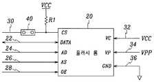
도 5는 이 발명의 실시예에 따른 고정된 플래시 롬의 데이터 갱신이 가능한 컴퓨터 시스템에서 원본 플래시 롬이 장착되기 전의 회로도이다.5 is a circuit diagram before an original flash ROM is mounted in a computer system capable of updating data of a fixed flash ROM according to an embodiment of the present invention.
도 5에 도시되어 있듯이, 이 발명의 실시예에 따른 고정된 플래시 롬의 데이터 갱신이 가능한 컴퓨터 시스템에서 플래시 롬(20)에 연결되는 신호선은 데이터 선(22), 어드레스(address) 선(24), 어드레스 스트로브(strobe) 선(26), 출력 이네이블(enable) 선(28), 칩 선택 선(30), 전원선(32, 34, 36) 등이다.As shown in FIG. 5, in a computer system capable of updating data of a fixed flash ROM according to an embodiment of the present invention, a signal line connected to the
여기에서 칩 선택 선(30)은 점퍼(jumper)(40)로 연결되어 있기 때문에 외부에서 단속 가능하다.Here, the chip
도 6은 이 발명의 실시예에 따른 고정된 플래시 롬의 데이터 갱신이 가능한 컴퓨터 시스템에서 원본 플래시 롬이 장착되기 전의 메인 보드(main board)를 도시한 도면이다.FIG. 6 is a diagram illustrating a main board before an original flash ROM is mounted in a computer system capable of updating data in a fixed flash ROM according to an exemplary embodiment of the present invention.
도 6에 도시되어 있듯이, 이 발명의 실시예에 따른 고정된 플래시 롬의 데이터 갱신이 가능한 컴퓨터 시스템의 메인 보드(50)에는 플래시 롬(20)이 장착되어 있고, 플래시 롬(20)의 칩 선택 선(30)이 점퍼(40)에 의해 연결되도록 되어 있다.As illustrated in FIG. 6, a
도 7은 이 발명의 실시예에 따른 고정된 플래시 롬의 데이터 갱신이 가능한 컴퓨터 시스템에서 원본 플래시 롬을 메인 보드 상에 장착하기 위한 연결을 도시한 도면이다.7 is a diagram illustrating a connection for mounting an original flash ROM on a main board in a computer system capable of updating data of a fixed flash ROM according to an embodiment of the present invention.
도 7에 도시되어 있듯이, 이 발명의 실시예에 따른 고정된 플래시 롬의 데이터 갱신이 가능한 컴퓨터 시스템에서 플래시 롬 소켓(60)은 플래시 롬(20) 위로 장착되어 플래시 롬(20)이 플래시 롬 소켓(60)으로 삽입된다. 또한, 원본 플래시 롬(70)은 플래시 롬 소켓(60)의 위에 삽입된다. 한편, 원본 플래시 롬(70)의 칩 선택 선(80)은 점퍼(90)에 따로 연결된다.As shown in FIG. 7, in a computer system capable of updating data of a fixed flash ROM according to an embodiment of the present invention, a
도 8은 이 발명의 실시예에 따른 고정된 플래시 롬의 데이터 갱신이 가능한 컴퓨터 시스템에서 원본 플래시 롬(70)이 플래시 롬 소켓(60)을 통해 메인 보드의 플래시 롬(20)에 접속된 것을 도시한 도면이다.8 illustrates that the
도 8에 도시되어 있듯이, 고정된 플래시 롬의 데이터 갱신이 가능한 컴퓨터 시스템에서 원본 플래시 롬(70)이 플래시 롬 소켓(60)에 장착되고, 플래시 롬 소켓(60)이 메인 보드(50)에 장착되어 있는 플래시 롬(20)에 장착되면, 원본 플래시 롬(70)과 플래시 롬(20)이 접속된다. 이 때, 플래시 롬(20)에 연결되는 칩 선택 선(30)을 연결하는 점퍼(40)가 제거되고, 원본 플래시 롬(70)의 칩 선택 선(80)을 칩 선택 선(30)에 연결하는 점퍼(90)가 연결된다.As shown in FIG. 8, in a computer system capable of updating data of a fixed flash ROM, an
도 9는 이 발명의 실시예에 따른 고정된 플래시 롬의 데이터 갱신이 가능한 컴퓨터 시스템에서 원본 플래시 롬(70)이 플래시 롬 소켓(60)을 통해 메인 보드의 플래시 롬(20)에 접속된 회로도이다.9 is a circuit diagram in which an
도 9에 도시되어 있듯이, 이 발명의 실시예에 따른 고정된 플래시 롬의 데이터 갱신이 가능한 컴퓨터 시스템에서 플래시 롬(20)에 연결되는 신호선인 데이터 선(22), 어드레스 선(24), 어드레스 스트로브 선(26), 출력 이네이블 선(28), 전원선(32, 34, 36) 등이 모두 플래시 롬 소켓(60)을 통해 원본 플래시 롬(60)에 연결되고, 플래시 롬(20)에 연결된 칩 선택 선(30)이 원본 플래시 롬(70)의 칩 선택 선(80)에 연결된다.As shown in FIG. 9, a
도 10은 이 발명의 실시예에 따른 고정된 플래시 롬의 데이터 갱신이 가능한 컴퓨터 시스템의 제어 방법의 순서도이다.10 is a flowchart illustrating a control method of a computer system capable of updating data of a fixed flash ROM according to an embodiment of the present invention.
도 10에 도시되어 있듯이, 이 발명의 실시예에 따른 고정된 플래시 롬의 데이터 갱신이 가능한 컴퓨터 시스템의 제어 방법은 메인 보드(50)에 장착된 플래시 롬(20)이 동작하지 않도록 하는 단계(S10)와; 플래시 롬 소켓(60)을 통해 원본 플래시 롬(70)을 플래시 롬(20)에 접속하는 단계(S11)와; 컴퓨터의 전원을 온시키는 단계(S12)와; 원본 플래시 롬(70)이 동작하지 않도록 하는 단계(S13)와; 플래시 롬(20)이 동작하도록 하는 단계(S14)와; 플래시 롬 갱신 프로그램을 실행시키는 단계(S15)와; 플래시 롬(20)의 데이터를 갱신하는 단계(S16)와; 컴퓨터의 전원을 오프시키는 단계(S17)와; 플래시 롬 소켓(60)을 플래시 롬(20)으로부터 탈착시키는 단계(S18)를 포함한다.As shown in FIG. 10, in the method of controlling a computer system capable of updating data in a fixed flash ROM according to an embodiment of the present invention, the step of preventing the
상기한 구성에 의한, 이 발명의 실시예에 따른 고정된 플래시 롬의 데이터 갱신이 가능한 컴퓨터 시스템의 작용은 다음과 같다.With the above configuration, the operation of the computer system capable of updating the data in the fixed flash ROM according to the embodiment of the present invention is as follows.
먼저, 컴퓨터의 메인 보드(50) 상에 장착되어 고정된 플래시 롬(20)에 원본 플래시 롬(70)을 장착하기 위해 컴퓨터의 전원을 끈다.First, the computer is turned off to mount the
메인 보드(50)에 장착된 플래시 롬(20)에 저장된 OS로 부팅(booting)시키지 않기 위해 플래시 롬(20)이 동작하지 않도록 한다(S10).The
이와 같이 플래시 롬(20)이 동작하지 않도록 하는 데에는 여러 가지 방법이 있지만, 여기에서는 칩 선택 신호(30)가 연결되지 않도록 하는 것이다.As described above, there are various methods for preventing the
칩 선택 신호(30)의 연결을 끊기 위해서 점퍼(40)를 제거시키면 플래시 롬(20)으로 연결되는 칩 선택 신호(30)가 끊어지게 된다.When the
다음에, 플래시 롬(20) 대신에 원본 플래시 롬(70)에 저장된 OS로 부팅시키기 위해 원본 플래시 롬(70)을 플래시 롬(20) 위에 장착시켜야 한다.Next, the
즉, 원본 플래시 롬(70)을 플래시 롬 소켓(60) 위에 장착한 후, 플래시 롬 소켓(60)의 아랫 부분에 플래시 롬(20)을 삽입시켜서 플래시 롬(20) 위에 장착한다(S11).That is, after the
이렇게 하면, 플래시 롬(20)에 연결된 각종 신호선, 예를 들어 데이터 선(22), 어드레스 선(24), 어드레스 스트로브 선(26), 그리고 출력 이네이블 선(28) 등이 원본 플래시 롬(70)에 연결된다.In this way, various signal lines connected to the
이 때, 원본 플래시 롬(70)의 칩 선택 선(80)은 플래시 롬(20)의 칩 선택 선에 연결되지 않고, 점퍼(90)를 통해 메인 보드(50) 상에 있는 칩 선택 선(30)에 연결된다.At this time, the chip
이와 같이, 원본 플래시 롬(70)과 플래시 롬(20)을 접속시킨 후, 컴퓨터의 전원을 온시킨다(S12).In this way, after the
컴퓨터의 전원이 온되면, 플래시 롬(20)은 동작하지 않고 대신에 원본 플래시 롬(70)이 동작하여, 원본 플래시 롬(70)에 저장된 OS가 실행된다.When the computer is powered on, the
원본 플래시 롬(70)이 동작되어 사용자 환경이 구축되면, 원본 플래시 롬(70)의 OS가 램(RAM) 내에 복사되어 램의 OS가 실행되기 때문에 원본 플래시 롬(70)에 대한 억세스(access)가 없기 때문에, 원본 플래시 롬(70)은 제거되어도 상관이 없게 되므로, 원본 플래시 롬(70)의 칩 선택 선(80)을 끊기 위해 점퍼(90)를 제거시킨다(S13).When the
다음에, 플래시 롬(20) 데이터를 갱신하기 위해서 플래시 롬(20)이 동작되도록 하여야 하기 때문에 점퍼(40)를 연결하여 플래시 롬(20)의 칩 선택 선(30)을 연결시킨다(S14).Next, since the
이와 같이, 컴퓨터가 사용자 환경에 있고, 데이터가 갱신되어야 할 플래시 롬(20)이 연결되면, 사용자는 플래시 롬 갱신 프로그램을 실행시킨다(S15).In this manner, when the computer is in the user environment and the
이러한 플래시 롬 갱신 프로그램은 하드 디스크에 있거나 플로피 디스크에 저장되어 있다.This flash ROM update program may be on a hard disk or stored on a floppy disk.
또한, 갱신되어야 할 플래시 롬의 원본 데이터나 업그레이드 데이터도 하드 디스크 또는 플로피 디스크에 저장되어 있어야 한다.In addition, the original data or upgrade data of the flash ROM to be updated must also be stored on a hard disk or floppy disk.
상기 단계(S15)에서 플래시 롬 갱신 프로그램이 실행되면, 사용자는 원본 데이터나 업그레이드 데이터를 플래시 롬(20)에 기록하여 플래시 롬(20)의 데이터를 갱신시킨다(S16).When the flash ROM update program is executed in the step S15, the user writes original data or upgrade data to the
상기와 같이, 플래시 롬(20)의 데이터가 갱신되면 플래시 롬(20)의 데이터, 즉 OS로 다시 부팅하기 위해서 컴퓨터의 전원을 오프시킨다(S17).As described above, when the data of the
플래시 롬(20)의 데이터 갱신이 끝났기 때문에 플래시 롬 소켓(60)을 플래시 롬(20)으로부터 탈착시켜서 원본 플래시 롬(70)과 플래시 롬(20)의 접속을 끊는다(S18).Since the data update of the
다음에, 컴퓨터의 전원을 다시 켜면 갱신된 데이터가 저장된 플래시 롬(20)에 의해 컴퓨터가 부팅된다.Next, when the computer is turned on again, the computer is booted by the
이상에서와 같이 이 발명의 실시예에서, 컴퓨터 시스템 및 제어 장치의 PCB에서 플래시 롬을 분리시키지 않고, PCB에 플래시 롬이 실장된 상태에서 직접 데이터를 갱신함으로써, 시간적, 인적 낭비를 줄이고, PCB 등에 가해질 물리적인 손상을 방지할 수 있는 고정된 플래시 롬 데이터의 갱신이 가능한 컴퓨터 시스템 및 그 제어 방법을 제공할 수 있다.As described above, in the embodiment of the present invention, by directly updating data in a state where the flash ROM is mounted on the PCB without separating the flash ROM from the PCB of the computer system and the control device, time and human waste are reduced, A computer system capable of updating fixed flash ROM data capable of preventing physical damage to be applied and a control method thereof can be provided.
Claims (6)
Translated fromKoreanPriority Applications (4)
| Application Number | Priority Date | Filing Date | Title |
|---|---|---|---|
| KR1019970062326AKR100280637B1 (en) | 1997-11-24 | 1997-11-24 | Computer system capable of data update of fixed flash ROM and its control method |
| US09/198,407US6233681B1 (en) | 1997-11-24 | 1998-11-24 | Computer system and a control method of the same for in-system reprogramming of a fixed flash ROM when access to the fixed flash ROM is not possible |
| JP33331398AJPH11242592A (en) | 1997-11-24 | 1998-11-24 | Data update device and data update method for fixed flash ROM |
| TW087119539ATW379306B (en) | 1997-11-24 | 1998-11-24 | Computer system and a control method of the same for in-system reprogramming of a fixed flash ROM when access to the fixed flash ROM is not possible |
Applications Claiming Priority (1)
| Application Number | Priority Date | Filing Date | Title |
|---|---|---|---|
| KR1019970062326AKR100280637B1 (en) | 1997-11-24 | 1997-11-24 | Computer system capable of data update of fixed flash ROM and its control method |
Publications (2)
| Publication Number | Publication Date |
|---|---|
| KR19990041698A KR19990041698A (en) | 1999-06-15 |
| KR100280637B1true KR100280637B1 (en) | 2001-02-01 |
Family
ID=19525437
Family Applications (1)
| Application Number | Title | Priority Date | Filing Date |
|---|---|---|---|
| KR1019970062326AExpired - Fee RelatedKR100280637B1 (en) | 1997-11-24 | 1997-11-24 | Computer system capable of data update of fixed flash ROM and its control method |
Country Status (4)
| Country | Link |
|---|---|
| US (1) | US6233681B1 (en) |
| JP (1) | JPH11242592A (en) |
| KR (1) | KR100280637B1 (en) |
| TW (1) | TW379306B (en) |
Families Citing this family (24)
| Publication number | Priority date | Publication date | Assignee | Title |
|---|---|---|---|---|
| US6715074B1 (en)* | 1999-07-27 | 2004-03-30 | Hewlett-Packard Development Company, L.P. | Virus resistant and hardware independent method of flashing system bios |
| US6715067B1 (en)* | 1999-09-21 | 2004-03-30 | Intel Corporation | Initializing a processor-based system from a non-volatile re-programmable semiconductor memory |
| US6535780B1 (en)* | 1999-11-10 | 2003-03-18 | Data I/O Corporation | High speed programmer system |
| KR100388961B1 (en)* | 2000-12-19 | 2003-06-25 | 엘지전자 주식회사 | data restoring control device of the flash ROM in the information processing system |
| US20020091917A1 (en)* | 2001-01-05 | 2002-07-11 | Cheng-Chi Liao | Method for control of multiple operating systems and electronic machines applicable thereto |
| US6842855B2 (en)* | 2001-01-26 | 2005-01-11 | Dell Products L.P. | System and method for providing information to a computer system |
| US6651188B2 (en)* | 2001-06-29 | 2003-11-18 | Intel Corporation | Automatic replacement of corrupted BIOS image |
| KR100806104B1 (en)* | 2001-11-28 | 2008-02-21 | 엘지전자 주식회사 | How to upgrade software on digital home appliances |
| US7779407B2 (en)* | 2002-05-29 | 2010-08-17 | Adams Phillip M | Computer-hardware, life-extension apparatus and method |
| CN100364013C (en)* | 2002-09-07 | 2008-01-23 | 鸿富锦精密工业(深圳)有限公司 | Method and device for storing check code in flash memory |
| DE10244975B4 (en)* | 2002-09-26 | 2005-08-04 | Siemens Ag | Method for updating the operating software of a device |
| CN100390737C (en)* | 2005-01-25 | 2008-05-28 | 英业达股份有限公司 | Method for automatically updating and backing up BIOS |
| US20070277028A1 (en)* | 2006-05-26 | 2007-11-29 | Jamey Cates | Method and system for recovery from reprogramming failures in nonvolatile memory |
| GB2441157B (en)* | 2006-08-25 | 2008-08-27 | Giga Byte Technology Company L | External basic input/output system device |
| US20080126777A1 (en)* | 2006-08-28 | 2008-05-29 | Giga-Byte Technology Co.,Ltd. | External basic input/output system device |
| US7509544B2 (en)* | 2007-02-26 | 2009-03-24 | Inventec Corporation | Data repair and synchronization method of dual flash read only memory |
| US8078836B2 (en) | 2007-12-30 | 2011-12-13 | Intel Corporation | Vector shuffle instructions operating on multiple lanes each having a plurality of data elements using a common set of per-lane control bits |
| CN102479088A (en)* | 2010-11-25 | 2012-05-30 | 鸿富锦精密工业(深圳)有限公司 | BIOS refreshing device |
| EP2568407B1 (en)* | 2011-09-09 | 2017-10-25 | Assa Abloy Ab | Method and system for communicating with and programming a secure element |
| US8954698B2 (en) | 2012-04-13 | 2015-02-10 | International Business Machines Corporation | Switching optically connected memory |
| US9098302B2 (en)* | 2012-06-28 | 2015-08-04 | Intel Corporation | System and apparatus to improve boot speed in serial peripheral interface system using a baseboard management controller |
| US9703697B2 (en) | 2012-12-27 | 2017-07-11 | Intel Corporation | Sharing serial peripheral interface flash memory in a multi-node server system on chip platform environment |
| CN103544040A (en)* | 2013-10-31 | 2014-01-29 | 无锡市矽成微电子有限公司 | Rapid programming device |
| CN105575836B (en)* | 2014-10-08 | 2018-06-12 | 慧荣科技股份有限公司 | Testing device |
Family Cites Families (8)
| Publication number | Priority date | Publication date | Assignee | Title |
|---|---|---|---|---|
| US5473775A (en) | 1991-10-11 | 1995-12-05 | Kabushiki Kaisha Toshiba | Personal computer using flash memory as BIOS-ROM |
| US5471674A (en) | 1992-02-07 | 1995-11-28 | Dell Usa, L.P. | Computer system with plug-in override of system ROM |
| US5634079A (en) | 1992-05-15 | 1997-05-27 | Zenith Data Systems Corporation | System for providing for a parallel port with standard signals and a flash recovery mode with second predetermined signals redefining parallel port with alternate functions |
| US5327531A (en)* | 1992-09-21 | 1994-07-05 | International Business Machines Corp. | Data processing system including corrupt flash ROM recovery |
| US5568641A (en) | 1995-01-18 | 1996-10-22 | Hewlett-Packard Company | Powerfail durable flash EEPROM upgrade |
| KR0172001B1 (en)* | 1995-12-05 | 1999-03-30 | 윤종용 | Re-programming apparatus of bios memory |
| KR100198382B1 (en)* | 1996-05-07 | 1999-06-15 | 윤종용 | Computer with multi-booting function |
| US5805882A (en) | 1996-07-19 | 1998-09-08 | Compaq Computer Corporation | Computer system and method for replacing obsolete or corrupt boot code contained within reprogrammable memory with new boot code supplied from an external source through a data port |
- 1997
- 1997-11-24KRKR1019970062326Apatent/KR100280637B1/ennot_activeExpired - Fee Related
- 1998
- 1998-11-24USUS09/198,407patent/US6233681B1/ennot_activeExpired - Lifetime
- 1998-11-24TWTW087119539Apatent/TW379306B/ennot_activeIP Right Cessation
- 1998-11-24JPJP33331398Apatent/JPH11242592A/enactivePending
Also Published As
| Publication number | Publication date |
|---|---|
| JPH11242592A (en) | 1999-09-07 |
| US6233681B1 (en) | 2001-05-15 |
| TW379306B (en) | 2000-01-11 |
| KR19990041698A (en) | 1999-06-15 |
Similar Documents
| Publication | Publication Date | Title |
|---|---|---|
| KR100280637B1 (en) | Computer system capable of data update of fixed flash ROM and its control method | |
| US5987536A (en) | Computer system having flash memory bios which can be accessed while protected mode operating system is running | |
| US7003655B2 (en) | Detection circuit and method for clearing BIOS configuration memory | |
| US6904484B1 (en) | Low pin count (LPC) firmware hub recovery | |
| US6000005A (en) | Method of writing a flash memory including dynamically switching and allocating memory spaces to the flash memory blocks | |
| KR100223844B1 (en) | Optional automatic setting circuit | |
| JPH02139612A (en) | Cartridge connecting circuit | |
| JPH11149376A (en) | Boot loader circuit | |
| US6539472B1 (en) | Reboot control unit and reboot control method | |
| US7010680B2 (en) | ROM writer has switching device for switching between external start-up ROM and data ROM to update control program in built-in writable ROM | |
| KR100256522B1 (en) | I/o memory card type pager | |
| JP2022120434A (en) | Information processing device, method for disabling management engine, and program | |
| JPH10283172A (en) | Flash rom data rewrite system | |
| JPH07281986A (en) | Extended board, information processor using the same and control method for peripheral device | |
| KR100467514B1 (en) | How to light a BIOS image | |
| KR930005778Y1 (en) | Universal ROM Writer Circuit in Computer Systems | |
| JP2001318907A (en) | Microcomputer incorporating flash memory | |
| JP2000029673A (en) | Program control system | |
| JP4174272B2 (en) | Device controller | |
| JPH11175345A (en) | Programmable controller | |
| KR100476555B1 (en) | Card jig device for programming PC memory card | |
| JP2839631B2 (en) | Personal computer system and configuration change method thereof | |
| JP3405239B2 (en) | Initial value setting change device | |
| JPH11272642A (en) | 1-chip microcomputer and start address setting method | |
| JPH07193860A (en) | Mobile terminal device having program memory |
Legal Events
| Date | Code | Title | Description |
|---|---|---|---|
| A201 | Request for examination | ||
| PA0109 | Patent application | St.27 status event code:A-0-1-A10-A12-nap-PA0109 | |
| PA0201 | Request for examination | St.27 status event code:A-1-2-D10-D11-exm-PA0201 | |
| R17-X000 | Change to representative recorded | St.27 status event code:A-3-3-R10-R17-oth-X000 | |
| R18-X000 | Changes to party contact information recorded | St.27 status event code:A-3-3-R10-R18-oth-X000 | |
| PN2301 | Change of applicant | St.27 status event code:A-3-3-R10-R13-asn-PN2301 St.27 status event code:A-3-3-R10-R11-asn-PN2301 | |
| PG1501 | Laying open of application | St.27 status event code:A-1-1-Q10-Q12-nap-PG1501 | |
| PN2301 | Change of applicant | St.27 status event code:A-3-3-R10-R13-asn-PN2301 St.27 status event code:A-3-3-R10-R11-asn-PN2301 | |
| E902 | Notification of reason for refusal | ||
| PE0902 | Notice of grounds for rejection | St.27 status event code:A-1-2-D10-D21-exm-PE0902 | |
| T11-X000 | Administrative time limit extension requested | St.27 status event code:U-3-3-T10-T11-oth-X000 | |
| P11-X000 | Amendment of application requested | St.27 status event code:A-2-2-P10-P11-nap-X000 | |
| P13-X000 | Application amended | St.27 status event code:A-2-2-P10-P13-nap-X000 | |
| R18-X000 | Changes to party contact information recorded | St.27 status event code:A-3-3-R10-R18-oth-X000 | |
| E701 | Decision to grant or registration of patent right | ||
| PE0701 | Decision of registration | St.27 status event code:A-1-2-D10-D22-exm-PE0701 | |
| GRNT | Written decision to grant | ||
| PR0701 | Registration of establishment | St.27 status event code:A-2-4-F10-F11-exm-PR0701 | |
| PR1002 | Payment of registration fee | St.27 status event code:A-2-2-U10-U11-oth-PR1002 Fee payment year number:1 | |
| PG1601 | Publication of registration | St.27 status event code:A-4-4-Q10-Q13-nap-PG1601 | |
| R17-X000 | Change to representative recorded | St.27 status event code:A-5-5-R10-R17-oth-X000 | |
| PN2301 | Change of applicant | St.27 status event code:A-5-5-R10-R13-asn-PN2301 St.27 status event code:A-5-5-R10-R11-asn-PN2301 | |
| R18-X000 | Changes to party contact information recorded | St.27 status event code:A-5-5-R10-R18-oth-X000 | |
| R18-X000 | Changes to party contact information recorded | St.27 status event code:A-5-5-R10-R18-oth-X000 | |
| PR1001 | Payment of annual fee | St.27 status event code:A-4-4-U10-U11-oth-PR1001 Fee payment year number:4 | |
| R18-X000 | Changes to party contact information recorded | St.27 status event code:A-5-5-R10-R18-oth-X000 | |
| PR1001 | Payment of annual fee | St.27 status event code:A-4-4-U10-U11-oth-PR1001 Fee payment year number:5 | |
| PN2301 | Change of applicant | St.27 status event code:A-5-5-R10-R13-asn-PN2301 St.27 status event code:A-5-5-R10-R11-asn-PN2301 | |
| PN2301 | Change of applicant | St.27 status event code:A-5-5-R10-R13-asn-PN2301 St.27 status event code:A-5-5-R10-R11-asn-PN2301 | |
| PR1001 | Payment of annual fee | St.27 status event code:A-4-4-U10-U11-oth-PR1001 Fee payment year number:6 | |
| PR1001 | Payment of annual fee | St.27 status event code:A-4-4-U10-U11-oth-PR1001 Fee payment year number:7 | |
| PR1001 | Payment of annual fee | St.27 status event code:A-4-4-U10-U11-oth-PR1001 Fee payment year number:8 | |
| FPAY | Annual fee payment | Payment date:20080604 Year of fee payment:9 | |
| PR1001 | Payment of annual fee | St.27 status event code:A-4-4-U10-U11-oth-PR1001 Fee payment year number:9 | |
| LAPS | Lapse due to unpaid annual fee | ||
| PC1903 | Unpaid annual fee | St.27 status event code:A-4-4-U10-U13-oth-PC1903 Not in force date:20091111 Payment event data comment text:Termination Category : DEFAULT_OF_REGISTRATION_FEE | |
| PC1903 | Unpaid annual fee | St.27 status event code:N-4-6-H10-H13-oth-PC1903 Ip right cessation event data comment text:Termination Category : DEFAULT_OF_REGISTRATION_FEE Not in force date:20091111 | |
| R18-X000 | Changes to party contact information recorded | St.27 status event code:A-5-5-R10-R18-oth-X000 | |
| P22-X000 | Classification modified | St.27 status event code:A-4-4-P10-P22-nap-X000 | |
| P22-X000 | Classification modified | St.27 status event code:A-4-4-P10-P22-nap-X000 |