KR100279767B1 - Apparatus for testing flash memory - Google Patents
Apparatus for testing flash memoryDownload PDFInfo
- Publication number
- KR100279767B1 KR100279767B1KR1019970040024AKR19970040024AKR100279767B1KR 100279767 B1KR100279767 B1KR 100279767B1KR 1019970040024 AKR1019970040024 AKR 1019970040024AKR 19970040024 AKR19970040024 AKR 19970040024AKR 100279767 B1KR100279767 B1KR 100279767B1
- Authority
- KR
- South Korea
- Prior art keywords
- flash memory
- data
- address
- test
- write
- Prior art date
- Legal status (The legal status is an assumption and is not a legal conclusion. Google has not performed a legal analysis and makes no representation as to the accuracy of the status listed.)
- Expired - Fee Related
Links
Images


Classifications
- G—PHYSICS
- G11—INFORMATION STORAGE
- G11C—STATIC STORES
- G11C29/00—Checking stores for correct operation ; Subsequent repair; Testing stores during standby or offline operation
- G—PHYSICS
- G11—INFORMATION STORAGE
- G11C—STATIC STORES
- G11C29/00—Checking stores for correct operation ; Subsequent repair; Testing stores during standby or offline operation
- G11C29/52—Protection of memory contents; Detection of errors in memory contents
Landscapes
- For Increasing The Reliability Of Semiconductor Memories (AREA)
- Tests Of Electronic Circuits (AREA)
Abstract
Translated fromKoreanDescription
Translated fromKorean본 발명은 플래시 메모리(Flash Memory)의 불량 여부(良否)를 판정함과 동시에, 플래시 메모리의 어드레스마다 데이타 기록 성공까지의 횟수를 측정하고, 연산 처리하며, 그 분포 상황을 해석하여 표시하는 플래시 메모리 시험 장치에 관한 것이다.The present invention provides a flash memory for determining whether a flash memory is defective or not, measuring the number of times until a data write is successful for each address of the flash memory, performing arithmetic processing, and analyzing and displaying the distribution state. It relates to a test apparatus.
플래시 메모리란, 재기록 가능한 독출 전용 메모리인 PROM 중, 전기적으로 모든 비트 단위 또는 블록 단위로 내용을 소거하고, 재기록이 가능한 비휘발성 메모리 IC이다. 즉, 대용량이고, 다수회의 재기록 가능한 비휘발성 메모리로서, 데이타의 독출 모드, 기록 모드(프로그램 모드), 기록 검증 모드(프로그램 검증 모드), 소거 모드, 기타의 일련의 동작 모드가 구비되어 있다. 이들 동작은 메모리 내부의 제어기에 외부로부터의 각각의 특정 명령을 기록 인에이블(WE) 신호에 의해 기록함으로써 제어된다. 플래시 메모리는 이 명령을 입력하는 단자로서 전용 단자는 가지고 있지 않으며, 데이타 단자와 공용하고 있고, 그 데이타와 명령의 전환은 예컨대, 특정 전원 단자의 전압을 변경시킴으로써 실행되고 있다. 본원 명세서에서는 기록 동작에 관하여 상세히 설명하고 있지만, 소거 동작에 대해서도 기록 동작과 동일하기 때문에 그 설명을 생략한다.The flash memory is a nonvolatile memory IC capable of electrically erasing and rewriting contents in PROM, which is a rewritable read-only memory. That is, as a large-capacity, rewritable nonvolatile memory, a read mode, a write mode (program mode), a write verify mode (program verify mode), an erase mode, and a series of other operation modes are provided. These operations are controlled by writing each specific command from the outside to a controller inside the memory by means of a write enable (WE) signal. The flash memory has a dedicated terminal as a terminal for inputting this command and does not have a dedicated terminal. The flash memory is shared with the data terminal, and switching between the data and the command is performed by changing a voltage of a specific power supply terminal, for example. In the present specification, the write operation is described in detail, but the erase operation is also the same as the write operation, and thus the description thereof is omitted.
그런데, 플래시 메모리는 그 구조상, 각 어드레스에서의 기록에 있어서 1회의 기록 동작으로 데이타 기록이 성공한다고는 할 수 없다. 그래서, 통상은 복수회 기록 동작을 반복할 필요가 있다. 기록에 성공할 때까지의 횟수(이하 「기록 횟수」라고 한다)는 피시험 플래시 메모리(이하 「MUT」라고 한다)의 종류나 동일한 종류의 MUT에 있어서도 어드레스마다 상이하다. 또한, 플래시 메모리는 이미 데이타의 기록에 성공한 상태의 어드레스에 대해서는 재기록을 행해서는 안되는 사양(仕樣)으로 되어 있다. 그리고, 데이타의 기록 시험은 예컨대, 25회라고 하는 규정 횟수 이내에서 모든 어드레스의 메모리 셀에 데이타를 기록할 수 있는 경우에 이 MUT의 기록 시험은 양품(良品)으로 판단한다.By the way, in the flash memory, data writing is not successful in one write operation in writing at each address. Therefore, it is usually necessary to repeat the recording operation a plurality of times. The number of times until successful writing (hereinafter referred to as "write count") differs from address to address in the type of flash memory under test (hereinafter referred to as "MUT") or the same type of MUT. In addition, the flash memory has a specification that rewrite should not be performed for an address in which data has already been successfully written. The data write test is judged as good quality if the data can be written in the memory cells of all addresses within a prescribed number of times, for example, 25 times.
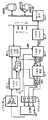
도 4에 종래의 플래시 메모리 시험 장치의 개략도를 도시한다. EWS(워크·스테이션)(10)로부터의 지시에 의해, 시험 프로세서(11)는 장치 전체의 제어를 행하고, 테스터·버스에 의해 각 유닛과의 사이에서 제어 신호나 데이타 신호 등의 송수신(授受)을 행한다. 타이밍 발생기(12)는 장치의 타이밍을 취하기 위해서 클록·타이밍 신호를 발생하여 패턴 발생기(13), 파형 정형기(14)나 논리 비교기(17) 등에 공급되는 시험의 타이밍을 취한다. 패턴 발생기(13)는 MUT(5)에 공급되는 제어 신호(CS), 예컨대 WE(기록 인에이블) 신호, 시험 패턴 신호(TPD), 어드레스 신호(ADRS)나, 논리 비교기(17)에 공급되는 기대치 패턴이나, 불량 해석 메모리(fail analysis memory)(18)에 공급되는 어드레스 신호 등을 발생시킨다.4 shows a schematic diagram of a conventional flash memory test apparatus. By the instruction from the EWS (work station) 10, the
파형 정형기(14)는 패턴 발생기(13)로부터의 3종류의 논리 신호를 시험 신호 파형으로 정형하고, 드라이버(15)를 통해 MUT(5)에 일련의 시험 신호를 공급한다. MUT(5)로부터의 응답 신호는 비교기(16)에서 전압 비교되어, 그 결과의 논리 신호를 논리 비교기(17)에 공급한다. 논리 비교기(17)에서는 비교기(16)로부터의 시험 결과 패턴과 패턴 발생기(13)로부터의 기대치 패턴을 논리 비교하여 일치·불일치가 검출되며, 불량 해석 메모리(18)에 결과 신호를 전송한다. 불량 해석 메모리(18)는 일치, 즉 매치(match)하는 어드레스에는 WE의 금지 신호 /WE 신호를 파형 정형기(14)에 공급하여 그 어드레스의 재기록 시험을 이후 금지하고, 그 외의 어드레스에 RETRY의 규정 횟수 또는 일치까지 기록 시험을 속행한다. 도중에서 모든 어드레스가 PASS(일치:매치)하면, MF(매치·플래그) 신호를 패턴 발생기(13)로 공급하여 종료하거나 또는 최대 규정 횟수까지 시험을 행하면 종료하여 다음 시험 항목으로 이행한다. 이 기록 시험 결과를 불량 해석 메모리(18)는 기억하여 MUT(5)의 불량 여부의 판정을 행한다.The waveform shaper 14 shapes three types of logic signals from the
EWS(10)에서는 모든 어드레스에 규정 횟수까지의 기록 시험을 행한 후에, 불량 해석 메모리(18)의 내용을 테스터·버스, 시험 프로세서(11)를 통해 독출한다. 이 독출된 불량 해석 메모리(18)의 정보에 기초하여 표시기에 불량 정보를 표시한다. 도시 생략하였지만, 예컨대, 비트 맵 표시로 불량 정보를 각 어드레스마다 또는 각 비트마다 양호·불량의 표시를 행한다. 일례로서, 어드레스마다 양호한 부분은 공백으로 하고, 불량인 부분에는 F를 표시한 양호·불량 맵이 있다.In the EWS 10, after the write test is performed for all addresses up to the prescribed number of times, the contents of the
도 5는 플래시 메모리의 기록 시험의 순서를 설명하는 도면이다. 도 4를 부가하여 설명한다. 도 5의 (a)는 파형 정형기(14)로부터 MUT(5)로 공급되는 3개의 신호로서, (a)의 어드레스 신호(ADRS)로 MUT(5)의 어드레스가 지정된다. (b)의 제어 신호(CS)에는 WE(기록 인에이블) 신호가 송출되고, WE가 로우일 때에 액티브(기록 가능)로 되어 있다. (c)의 시험 패턴 신호(TPD)에는 데이타 신호가 전송되고, 처음에 프로그램·셋업·모드의 명령을 송출 프로그램·모드로 설정한다. 다음에, 데이타를 전송하여 (a)의 어드레스에 데이타를 기록한다. 다음에, 이 기록 데이타를 유지한 채로 프로그램·검증·모드로 하고, 메모리 내부의 제어기는 데이타를 독출하여 기록 데이타, 즉 기대치 데이타와의 비교를 행한다. 일치하지 않을 경우에는 MUT(5)로부터 프로그램·불량 신호가 출력되기 때문에, 이 어드레스에 대해서는 기록은 실패(불량)로 판정된다. 모든 어드레스에 대해서, 이 일련의 동작을 반복 실행한다.5 is a diagram illustrating a procedure of a write test of a flash memory. It demonstrates adding FIG. FIG. 5A shows three signals supplied from the
도 5의 (b)는 상기한 기록 시험의 흐름도이다. 통상, 1회의 기록 시험만으로 모든 어드레스에 대해서 패스한다고는 할 수 없기 때문에, 2회째 이후의 시험에 있어서도 동일한 어드레스·시퀀스에 의해 복수회에 걸쳐서 시험을 행한다. 또한, 플래시 메모리에서는 이미 데이타의 기록에 성공한 상태의 어드레스에 대해서는 재기록을 행해서는 안되는 사양으로 되어 있다. 그래서, 전회까지의 시험 결과를 저장하고 있는 불량 해석 메모리(18)를 참조하여, 이미 패스된 상태의 어드레스에 대해서는 파형 정형기(14)로 /WE 신호를 송출하고, MUT(5)로의 WE 신호를 금지하고 있다.Fig. 5B is a flowchart of the above described recording test. Usually, since it is not possible to pass for all addresses by only one write test, the test is performed a plurality of times by the same address sequence even in the second and subsequent tests. In addition, in the flash memory, an address must not be rewritten to an address in which data has already been successfully written. Thus, referring to the
도 5의 (b)에 대해서 간단히 설명한다. 기록 시험의 개시에 있어서, S1 단계에서 RETRY를 1로 설정하고, S2 단계에서 ADDRESS를 0으로 설정한다. 다음에, PROGRAM 종료, 즉 기록 종료인지의 여부를 판단하여, no이면 기록 PROGRAM(S4), 독출 데이타와 기대치 데이타 비교의 검증[VERIFY](S5)을 행한다. S3에서 yes이면 불량 해석 메모리(18)로부터의 신호로 WE를 마스크 세트하여 재기록 동작을 금지한다. 다음에, 어드레스가 최대인지의 여부를 판정하여(S7), 도중이면 어드레스 번호를 +1(S8)하여 반복한다. 최대이면, 모든 기록이 종료했는지의 여부를 판정하여(S9), no인 경우에는 RETRY가 규정치인지의 여부를 판단하고(S10), 도달하고 있지 않을 경우에는 RETRY를 +1(S11)하여 반복한다. 기록 종료 또는 RETRY가 MAX가 되면, EWS(10)는 불량 해석 메모리(18)의 데이타를 독출하고(S12), 모든 데이타가 PASS하고 있는지의 여부를 판단하여(S13), yes는 양품으로 하고, no는 불량품으로 하고 있었다.5 (b) will be briefly described. At the start of the recording test, RETRY is set to 1 in step S1 and ADDRESS is set to 0 in step S2. Then, it is judged whether or not the end of PROGRAM, that is, the end of recording, and if no, the write PROGRAM (S4) and verification of the comparison between the read data and the expected value data [VERIFY] (S5). If yes in S3, the mask is set to WE as a signal from the
플래시 메모리의 불량 여부의 판별에 대해서는 종래의 시험 장치로 충분하다. 그러나, 플래시 메모리는 재기록 가능한 독출 전용 메모리이기 때문에 수명이 있고, 데이타의 재기록 가능 횟수가 유한하며, 더욱이 격차가 있다. 그래서 이 기록/소거 사이클의 재기록 가능 횟수를 예측할 수 있으면 유익하고, 이 재기록 가능 횟수를 보다 많게 할 수 있으면 이 플래시 메모리의 가치는 점점 증대한다.Conventional test apparatuses are sufficient for determining whether or not the flash memory is defective. However, since the flash memory is a rewritable read-only memory, the flash memory has a lifetime, a finite number of rewritable data, and further gaps. Therefore, it is beneficial to be able to predict the rewritable number of times of this write / erase cycle, and the value of this flash memory increases gradually if this rewritable number is made larger.
이 데이타의 재기록 가능 횟수를 좌우하는 원인의 하나로는 제조 공정에 있어서의 가공의 균일성에 있다는 것을 알 수 있었다. 본 발명은 이러한 원인을 추구하여, 플래시 메모리의 웨이퍼 단계에서 또는 칩 단계에서 각각의 어드레스에 있어서 기록이 성공할 때까지의 기록 횟수를 계측하고, 연산 처리하여 그 분포 상황을 X, Y 좌표축면에 표시하여 파악하며, 그 분포 상황이 균일하게 되도록 제조 공정으로 환원하여 기록 횟수의 균일성을 실현하고자 하는 것이다.It was found that one of the causes of the number of rewritable times of this data lies in the uniformity of processing in the manufacturing process. In order to solve this problem, the present invention measures the number of writes until successful writing at each address at the wafer stage or the chip stage of the flash memory, calculates the operation, and displays the distribution on the X and Y coordinate axes. It is intended to realize the uniformity of the number of recordings by reducing the manufacturing process so that the distribution state is uniform.
플래시 메모리의 기록이 성공할 때까지의 기록 횟수의 균일성은 제조 공정에 있어서 가공의 균일성과 상관되고, 이 균일성으로부터 실용상의 최소 기록/소거 사이클을 예측할 수 있고, 또한 플래시 메모리의 수명도 연장시킬 수 있다고 생각된다. 즉, 본 발명은 플래시 메모리의 불량 여부를 판정함과 동시에, 제조 공정에 있어서의 가공의 균일성의 판단을 행하여, 수명의 연장을 시사하는 데이타를 제공하는 플래시 메모리 시험 장치를 제공하는 것을 목적으로 한다.The uniformity of the number of writes until the successful writing of the flash memory is correlated with the uniformity of processing in the manufacturing process. From this uniformity, the practical minimum write / erase cycle can be predicted and the life of the flash memory can be extended. I think it is. That is, an object of the present invention is to provide a flash memory test apparatus which determines whether or not a flash memory is defective and judges the uniformity of processing in a manufacturing process to provide data suggesting prolongation of life. .
도 1은 본 발명의 일실시예의 구성도.1 is a block diagram of an embodiment of the present invention.
도 2는 본 발명의 워크스테이션(EWS)(20)의 표시기에 표시하는 피시험 플래시 메모리(MUT)의 각 어드레스마다 기록 횟수를 나타내는 표시의 일예의 표시도.Fig. 2 is a display diagram showing an example of a display showing the number of times of writing for each address of the flash memory under test (MUT) displayed on the display of the workstation (EWS) 20 of the present invention.
도 3은 도 1의 구성예에 있어서의 동작의 일례의 흐름도.3 is a flowchart of an example of the operation in the configuration example of FIG. 1;
도 4는 종래예의 구성도.4 is a block diagram of a conventional example.
도 5는 도 4의 예에 있어서의 종래의 동작 흐름도.5 is a flowchart of a conventional operation in the example of FIG.
〈도면의 주요 부분에 대한 부호의 설명〉<Explanation of symbols for main parts of drawing>
5 : MUT(피시험 플래시 메모리)5: MUT (Test Flash Memory)
10, 20 : EWS(워크스테이션)10, 20: EWS (Workstation)
11 : 시험 프로세서11: test processor
12 : 타이밍 발생기12: timing generator
13 : 패턴 발생기13: pattern generator
14 : 파형 정형기14: waveform shaper
15 : 드라이버15: driver
16 : 비교기16: comparator
17 : 논리 비교기17: logical comparator
18 : 불량 해석 메모리(fail analysis memory)18: failure analysis memory
21 : DISK(대용량 기억기)21: DISK (Mass Storage)
22 : 불량 카운터(fail counter)22: fail counter
상기 목적을 달성하기 위해서 본 발명은 먼저 계측의 순서로서, 처음에 어드레스를 0으로 하여 각 어드레스마다 기록이 성공할 때까지 기록 동작을 반복하고, 검증 OK, 즉 기록이 성공할 때까지 또는 규정 기록 횟수까지의 기록 횟수를 계측하여 그 횟수를 불량 해석 메모리에 기억하고, 다음에 어드레스를 +1하여 시험을 반복한다. 이 계측을 최대 어드레스까지, 즉 모든 어드레스에서 반복하여, 불량 해석 메모리에 각 어드레스마다의 기록 횟수를 기억시킨다. 그리고, 각 어드레스에서의 기록 횟수 계측의 고속화를 하기 위해서, 어드레스마다 지정의 시작에서 종료까지 게이트를 열어 기록 횟수를 계수하는 불량 카운터를 설치한다.In order to achieve the above object, the present invention firstly repeats the recording operation until the recording succeeds for each address with an address of 0 at first, and the verification is OK, that is, until the recording is successful or until the prescribed number of recordings. The number of times of recording is measured, and the number of times is stored in the failure analysis memory. Then, the address is +1 and the test is repeated. This measurement is repeated up to the maximum address, i.e., at all addresses, and the number of writes for each address is stored in the failure analysis memory. In order to speed up the measurement of the number of writes at each address, a defective counter is provided for counting the number of writes by opening the gate from the start of the designation to the end of each address.
모든 어드레스까지의 기록 동작이 종료하면, 불량 어드레스에 메모리된 모든 어드레스의 정보를 테스터·버스 및 시험 프로세서를 통해 대용량 기억기의 DISK로 전송한다. DISK에는 이미 상술한 불량 정보를 처리하는 각종 프로그램과 각종 화일이 준비되어 있고, CPU를 내장한 워크·스테이션(EWS)과 협동하여, 불량 어드레스의 정보가 전송되면 EWS의 CPU는 즉시 해석 처리를 행한다.When the write operation to all addresses is completed, the information of all addresses stored in the bad address is transferred to the DISK of the mass storage device through the tester bus and the test processor. DISK has already prepared various programs and files for processing the above-mentioned bad information, and cooperates with a workstation (EWS) having a built-in CPU, and when the information of the bad address is transmitted, the CPU of the EWS immediately performs an analysis process. .
해석 처리는 피시험 메모리(MUT)가 웨이퍼인 경우에는 블록마다 또는 칩마다 또는 어드레스마다 기록 횟수를 표시하는 처리를 행하고, MUT가 칩인 경우에는 어드레스마다 또는 비트마다 표시하는 처리 연산을 행한다. 처리 연산된 데이타는 EWS의 지시에 따라 예컨대, 각 어드레스마다의 기록 횟수가 숫자에 따라, 모양에 따라, 또는 색상에 따라 표시기에 표시하도록 한다. X, Y 좌표면에 표시하면 이해하기 쉽다. 또한, 실험 데이타가 겹쳐지는 것에 따른 예측에 의해, 실용상의 기록/소거 사이클 예측을 표시할 수도 있다. 물론, 이 기록 횟수의 표시 판단은 즉시 제조 행정에 반영하여, 제조 공정 개선의 시사를 행할 수 있다.The analysis processing performs processing for displaying the number of writes per block, for each chip, or for every address when the memory under test (MUT) is a wafer, and performs a processing operation for displaying every address or every bit when the MUT is a chip. The processed data is displayed in the display according to the EWS, for example, the number of times of writing for each address in accordance with the number, shape, or color. It is easy to understand when displayed on the X, Y coordinate plane. In addition, it is also possible to display practical recording / erase cycle prediction by the prediction that the experimental data overlaps. Of course, the display judgment of the number of recordings can be immediately reflected in the manufacturing stroke, and the production process improvement can be suggested.
발명의 실시의 형태를 실시예에 기초해서 도면을 참조하여 설명한다. 도 1에 본 발명의 일실시예의 구성도를, 도 2에 워크·스테이션(EWS)(20)의 표시기에 표시되는 일례의 표시도를, 도 3에 본 발명의 동작의 일례의 흐름도를 도시한다. 도 4의 구성과 대응하는 부분에는 동일한 부호를 붙인다.Embodiment of this invention is described with reference to drawings based on an Example. 1 is a block diagram of an embodiment of the present invention, FIG. 2 is a display diagram of an example displayed on a display of a workstation (EWS) 20, and FIG. 3 is a flowchart of an example of the operation of the present invention. . Parts corresponding to those in FIG. 4 are given the same reference numerals.
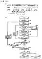
먼저, 동작의 흐름도인 도 3에 대해서 설명한다. 이 동작에서는 반드시 어드레스마다 기록이 성공할 때까지, 또는 최대 규정 횟수까지 기록 동작을 행하고, 기록 횟수를 카운터로 계측하여 불량 해석 메모리(18)에 기억시킨 후에, 다음 어드레스 번호를 변경하여 기록 동작을 속행시키고, 이 동작을 모든 어드레스에 대해서 실행한다.First, FIG. 3 which is a flowchart of an operation is demonstrated. In this operation, the recording operation must be performed until the recording succeeds for each address or up to the maximum prescribed number of times, and the number of recordings is measured by the counter and stored in the
계측의 개시에 의해, 처음에 S20 단계에서 어드레스(ADD)에 0을 설정하고, 다음에 S21에서 카운터(CONT)에 1을 설정한다. 그 후에 기록 동작에 들어가서, S22의 write program으로 데이타를 기록하고, S23의 data read로 기록된 데이타를 독출하며, S24의 verify 0K?로 기록 데이타와 독출 데이타의 일치·불일치를 대조한다.By the start of the measurement, first, 0 is set to the address ADD in step S20, and then 1 is set to the counter CONT in S21. Thereafter, the recording operation is started, the data is recorded by the write program of S22, the data recorded by the data read of S23 is read out, and the match and mismatch between the recorded data and the read data is checked by verify 0K?
불일치이면 S25에서 카운터치가 최대 규정치인지의 여부를 판단하여, no이면 S26에서 카운터치를 +1 하고, 다시 S22의 기록 동작을 반복한다. S24의 verify 0K? 또는 S25의 C0NT=MAX?가 yes이면 S27에서 그 카운터치를 불량 해석 메모리(18)에 기억시킨다. 다음에, S28에서 어드레스가 최대치인지의 여부를 판단하여, no이면 S29에서 어드레스치를 +1 하고, 다시 S21에서 카운터치를 1로 설정하여, 다음 어드레스에서의 기록 동작을 반복한다. 모든 어드레스의 기록 시험이 종료되면, S28에서 yes가 되므로 기록 동작 시험은 종료하고, 그 후 데이타의 정보 처리 동작으로 이동하며, 그 후에 어드레스마다의 시험 결과가 EWS 등의 표시기에 표시된다.If there is a mismatch, it is determined whether or not the counter value is the maximum prescribed value in S25. If no, the counter value is +1 in S26, and the recording operation of S22 is repeated. Verify 0K in S24? Or if C0NT = MAX? In S25, the counter value is stored in the
도 1은 상술한 동작을 행하는 본 발명의 일실시예의 구성도이다. 도 4의 설명과 중복하는 부분은 간략하게 설명한다. 이 시험 장치를 제어하는 시험 프로세서(11)와, 이 장치의 전체의 타이밍을 취하는 타이밍 발생기(12)와, 피시험 플래시 메모리(MUT)(5)로 공급하는 어드레스 신호(ADRS)와 시험 패턴 신호(TPD)와 제어 신호(CS) 이외에 기대치 신호를 발생하는 패턴 발생기(13)와, 이 패턴 발생기(13)로부터의 ADRS, TPD 및 CS의 각 신호를 파형 정형기(14)에서 시험 신호 파형으로 정형하여 드라이버(15)를 통해 MUT(5)로 공급하고, MUT(5)의 응답 신호를 비교기(16)를 통해 논리 비교기(17)에 공급한다.1 is a block diagram of an embodiment of the present invention for performing the above-described operation. Portions that overlap with the description of FIG. 4 will be briefly described. A
논리 비교기(17)는 MUT(5)로부터의 응답 신호와 패턴 발생기(13)로부터의 기대치 신호를 논리 비교하고 일치·불일치를 검출하여 불량 해석 메모리(18)로 전송한다. 불일치일 때에는 패턴 발생기(13)로부터 동일 어드레스에 다시 시험 패턴 신호(TPD)와 제어 신호(CS)를 MUT(5)로 전송하고, 일치할 때까지 또는 최대 규정 횟수까지 기록 동작을 반복함과 동시에, 불량 카운터(fail counter)(22)는 기록 횟수를 계수한다.The
불량 카운트는 프로그램에 의해서 CPU에서 행하여도 좋지만, 고속 동작을 행하기 위해서는 불량 카운터(22)를 설치하는 쪽이 좋다. 불량 카운터(22)는 동일 어드레스에서 1회째의 기록 개시로부터 verify OK, 즉 일치할 때까지 또는 최대 규정 횟수까지 게이트를 열어 이 동안의 기록 횟수를 계수한다. 게이트 신호는 도 1에서는 논리 비교기(17)로부터 수득하고 있지만, 패턴 발생기(13) 또는 불량 해석 메모리(18)로부터 수득하여도 좋다. 카운트 펄스도 도 1에서 파형 정형기(14)로부터의 제어 신호(CS)를 계수하도록 하고 있지만, 논리 비교기(17)의 불일치 펄스와 최후의 일치 펄스를 계측하여도 좋고, 패턴 발생기의 write program의 발생수를 계수하여도 좋다. 중요한 것은 동일 어드레스에서의 기록 횟수를 계수할 수 있으면 좋다. 이 불량 카운터(22)의 계수치를 불량 해석 메모리(18)로 전송하여 어드레스치와 함께 기억한다.The defect count may be performed by the CPU by a program. However, in order to perform high-speed operation, the
불량 해석 메모리(18)는 논리 비교기(17)로부터 일치 신호를 수신하면, 패턴 발생기(13)에 매치 플래그(MF) 신호를 전송하고, 패턴 발생기(13)에서는 어드레스치를 +1 하거나 또는 임의의 값으로 변경하여 필요한 범위의 어드레스의 시험을 행한다.When the
모든 어드레스 또는 측정하는 범위의 어드레스에서의 시험이 종료하면, 불량 해석 메모리(18)에 기억하고 있는 데이타를 데이타 버스 및 시험 프로세서(11)를 통해 대용량 기억기(DISK)(21)로 전송한다.When the test at all addresses or addresses in the measurement range ends, the data stored in the
DISK(21)에는 미리 표시 처리를 행하는 적어도 1개 이상의 처리 프로그램이 메모리되어 있고, 불량 해석 메모리(18)에 기억하고 있는 데이타가 전송되면 즉시또는 워크·스테이션(EWS)(20)으로부터의 지시에 의해, EWS(20)의 CPU와 협동하여 처리를 개시한다. DISK(21)에 준비되어 있는 처리 프로그램의 일예를 다음의 표 1에 나타낸다. 이 이외에, 복수 어드레스 사이에서 기록 성공까지의 횟수의 최대치, 최소치 및 평균치를 구하는 연산 프로그램도 준비되어 있다.The
먼저 처음에, ① 조건 설정 프로그램의 기동으로 조건 설정 데이타·화일의 작성을 행한다. 다음에, ② 디바이스 시험 프로그램의 기동으로 맵 관리 화일이나 논리 배치 재시도 데이타 화일의 작성을 행한다. 다음에, 불량 해석 메모리(18)로부터의 정보가 전송되면, ③ 재시도 데이타 이미지 변환 처리 프로그램이 가동하고, 대상 재시도 데이타 화일을 이미지 변환한다. 다음에, ④ 재시도 맵 출력 프로그램이 가동하여 표시기에 재시도 맵을 표시하고, ⑤ 맵 화일 정보 표시 처리 프로그램이 가동하여 맵 관리 화일이나 논리 배치 재시도 데이타 화일의 정보를 상기의 재시도 맵상에 표시한다.First, the condition setting data file is created by starting the condition setting program. Next, a map management file and a logical batch retry data file are created by starting the device test program. Next, when the information from the
이 표시의 일례를 도 2에 나타낸다. 도 2의 (a)는 MUT(5)로서 웨이퍼를 시험한 웨이퍼 맵 형태의 표시예이다. 기록 횟수의 구분을 복수개 설정하여 그 횟수에 들어 있는 분포 상황을 X, Y 좌표 상에 어드레스마다, 복수 어드레스의 부분마다 또는 칩마다 모양이나 기호나 색상으로 표시할 수 있다. 3차원의 막대 그래프로 표시하여도 좋다. 도 2의 (b)는 웨이퍼에 있어서의 각 칩마다의 칩 번호, 기록의 최대 횟수, 최소 횟수, 평균 횟수를 표시한 이산 리스트 형태예이다. 도 2의 (c)는 각 칩에 착안하여 칩의 X, Y 좌표 상에 어드레스마다의 기록 횟수를 표시한 칩 셀 좌표 형태예이다.An example of this display is shown in FIG. FIG. 2A is a display example in the form of a wafer map in which a wafer is tested as the
상술한 바와 같이 표시 도면에는 횟수치 그 자체, 모양이나 색상별로 변환한 것, 막대 그래프나 표층 그래프로 표시한 것 등의 여러가지 종류가 있지만, 중요한 것은 X, Y 좌표면에서 기록 횟수의 분포 상황이나 균일성을 일목 요연하게 알 수 있는 것이 바람직하다. 이 분포 상황에 따라 실용상 데이타의 기록/소거 사이클의 수명을 예측하여 상기의 표시기에 표시하여도 좋다. 또한, 기록 횟수가 균일해지도록 제조 공정을 개선하면 좋다.As described above, there are various types of display drawings, such as the number value itself, conversion by shape or color, and a bar graph or a surface graph. It is desirable to know uniformity at a glance. In accordance with this distribution situation, the lifetime of the data recording / erasing cycle may be predicted and displayed on the display. In addition, the manufacturing process may be improved so that the number of recordings becomes uniform.
상기 실시 형태에서는 도 1에 도시된 불량 카운터(22)와 불량 해석 메모리(18)가 별도의 구성 요소인 경우로 설명하였지만, 필요에 따라서 불량 해석 메모리(18)내의 메모리 데이타를 직접 누적 가산하는 연산 제어 수단으로 구성하여도 좋다.In the above embodiment, the
상기 실시의 형태에서는 모든 어드레스 또는 측정하는 범위의 어드레스에서의 이산 해석 형태로 설명하고 있었지만, 필요에 따라서 단시간에 모든 웨이퍼 또는 1칩 상의 이산 해석 시험에 있어서, 소정 메모리 셀을 샘플적으로 측정 실시하는 방법으로 해도 좋다. 즉, 메모리 셀 배치가 거의 등간격 위치에 있는 메모리 셀을 원하는 메모리 셀 간격 단위로 임의 추출 측정을 행하여 분포 상황을 표시한다. 이 때, 메모리 셀의 어드레스의 물리적 배열이, 예컨대 불량 셀 구제용의 메모리 구제 회로를 가지며 서로 상이하게 이루어진 경우나, 메모리 블록 배치가 서로 상이한 경우에는, 셀의 물리적 배치 관계를 정규화하기 위하여 종래 기술인 어드레스·스크램블러 기능을 이용하여 실시하는 것은 당연하다. 이 임의 추출의 일례로서는, 메모리 어드레스를 짝수 어드레스만 측정하든지, 2의 N승 단위 중의 1 어드레스를 측정하는 방법이라든지, 원하는 메모리 블록 단위 중의 1 어드레스의 수(또는 원하는 복수 어드레스의 수)를 측정하는 방법 등이 있다. 이것은 수 ㎛ 정도의 인접한 메모리 셀 사이에서는 통계적인 이산이 거의 발생되지 않는 것으로 간주한 해석 방법이다. 이 임의 추출 측정 방법에 의해서는 방대한 데이타 수집량이 대폭 경감될 수 있고, 또한 실용적이고 고속의 이산 해석 측정을 행할 수 있는 이점을 얻을 수 있다.Although the above embodiment has been described in the form of discrete analysis at all addresses or addresses in the measurement range, a predetermined memory cell is measured in a sample in a discrete analysis test on all wafers or one chip in a short time as needed. You may use it as a method. In other words, a random extraction measurement is performed for memory cells having almost identically spaced memory cell positions in units of a desired memory cell interval to display a distribution situation. In this case, when the physical arrangement of addresses of the memory cells is made different from each other with a memory rescue circuit for defective cell rescue, or when the memory block arrangements are different from each other, the conventional technique is used to normalize the physical arrangement relationship of the cells. It is natural to carry out using the address scrambler function. As an example of this random extraction, a memory address is measured only in even addresses, a method of measuring one address in two N-th power units, or a number (or desired number of multiple addresses) in one memory block unit is measured. Method and the like. This is an analysis method considered to have little statistical discreteness between adjacent memory cells on the order of several micrometers. By this arbitrary extraction measurement method, a large amount of data collection can be greatly reduced, and the advantage that a practical and high-speed discrete analysis measurement can be performed is obtained.
이상 상세히 설명한 바와 같이, 본 발명은 플래시 메모리 IC의 각 어드레스로의 데이타의 기록 성공까지의 횟수를 계수하여, 그 계측 데이타를 가공 처리하여 웨이퍼 단위 또는 칩 단위로 기록 성공까지의 횟수의 분포 상황을 X, Y 좌표축 상에서 이해하기 쉽게 표시하였다. 이 분포 상황은 제조 공정의 가공의 균일성에 상관하고 있고, 또한, 기록 성공까지의 횟수의 균일성은 플래시 메모리 IC의 기록/소거 사이클의 수명에도 상관하고 있으며, 그 수명을 예측할 수도 있다.As described in detail above, the present invention counts the number of times until successful writing of data to each address of the flash memory IC, processes the measurement data, and shows the distribution of the number of times until successful writing in the unit of wafer or chip. The X and Y coordinate axes are displayed for easy understanding. This distribution situation correlates to the uniformity of the processing of the manufacturing process, and the uniformity of the number of times until the writing success also correlates with the life of the write / erase cycle of the flash memory IC, and the life can be predicted.
또한, 플래시 메모리의 제조 공정의 가공 방법으로 환원하여 균일성을 더욱 향상시키는 것을 목표로 함으로써, 수명의 연장을 도모할 수 있다. 따라서, 본 발명은 기술적으로 커다란 효과를 갖는다.In addition, by aiming to further improve the uniformity by reducing the processing method of the flash memory manufacturing process, the life can be extended. Therefore, the present invention has a technically great effect.
Claims (6)
Translated fromKoreanApplications Claiming Priority (2)
| Application Number | Priority Date | Filing Date | Title |
|---|---|---|---|
| JP8279260AJPH10125092A (en) | 1996-10-22 | 1996-10-22 | Flash memory tester |
| JP96-279260 | 1996-10-22 |
Publications (2)
| Publication Number | Publication Date |
|---|---|
| KR19980032302A KR19980032302A (en) | 1998-07-25 |
| KR100279767B1true KR100279767B1 (en) | 2001-03-02 |
Family
ID=17608691
Family Applications (1)
| Application Number | Title | Priority Date | Filing Date |
|---|---|---|---|
| KR1019970040024AExpired - Fee RelatedKR100279767B1 (en) | 1996-10-22 | 1997-08-22 | Apparatus for testing flash memory |
Country Status (5)
| Country | Link |
|---|---|
| US (1) | US5896398A (en) |
| JP (1) | JPH10125092A (en) |
| KR (1) | KR100279767B1 (en) |
| DE (1) | DE19746695A1 (en) |
| TW (1) | TW372627U (en) |
Families Citing this family (38)
| Publication number | Priority date | Publication date | Assignee | Title |
|---|---|---|---|---|
| JP2000215688A (en)* | 1999-01-25 | 2000-08-04 | Mitsubishi Electric Corp | Semiconductor test apparatus and semiconductor test method |
| JP2001311766A (en) | 2000-04-28 | 2001-11-09 | Advantest Corp | Semiconductor device testing device and testing method |
| JP4601119B2 (en) | 2000-05-02 | 2010-12-22 | 株式会社アドバンテスト | Memory test method and memory test equipment |
| US6560729B1 (en) | 2000-07-03 | 2003-05-06 | Advanced Micro Devices, Inc. | Automated determination and display of the physical location of a failed cell in an array of memory cells |
| US6829737B1 (en)* | 2000-08-30 | 2004-12-07 | Micron Technology, Inc. | Method and system for storing device test information on a semiconductor device using on-device logic for determination of test results |
| US6748562B1 (en)* | 2000-10-31 | 2004-06-08 | Agilent Technologies, Inc. | Memory tester omits programming of addresses in detected bad columns |
| US6430096B1 (en) | 2000-11-01 | 2002-08-06 | International Business Machines Corporation | Method for testing a memory device with redundancy |
| DE10101234A1 (en)* | 2001-01-11 | 2002-07-18 | Giesecke & Devrient Gmbh | Testing non-volatile memory involves producing test pattern, write access to memory with test pattern, read access to acquire test result and comparison with test pattern for agreement |
| JP2003123499A (en)* | 2001-10-16 | 2003-04-25 | Mitsubishi Electric Corp | Semiconductor testing apparatus, semiconductor device testing method, and semiconductor device manufacturing method |
| JP4260434B2 (en)* | 2002-07-16 | 2009-04-30 | 富士通マイクロエレクトロニクス株式会社 | Nonvolatile semiconductor memory and operation method thereof |
| US20040015761A1 (en)* | 2002-07-22 | 2004-01-22 | Finisar Corporation | Scalable asynchronous I/O testing tool |
| US20040015762A1 (en)* | 2002-07-22 | 2004-01-22 | Finisar Corporation | Scalable system testing tools |
| KR100471006B1 (en)* | 2002-07-24 | 2005-03-10 | 삼성전자주식회사 | test system for testing jitter of high speed data output device and total jitter testing method |
| US6943575B2 (en)* | 2002-07-29 | 2005-09-13 | Micron Technology, Inc. | Method, circuit and system for determining burn-in reliability from wafer level burn-in |
| US7424659B2 (en)* | 2003-10-31 | 2008-09-09 | Sandisk Il Ltd. | System-in-package and method of testing thereof |
| KR100498509B1 (en)* | 2003-11-12 | 2005-07-01 | 삼성전자주식회사 | Flash memory test system capable of test time reduction and electrical test Method thereof |
| US7321951B2 (en)* | 2003-11-17 | 2008-01-22 | Micron Technology, Inc. | Method for testing flash memory power loss recovery |
| US7254763B2 (en)* | 2004-09-01 | 2007-08-07 | Agere Systems Inc. | Built-in self test for memory arrays using error correction coding |
| US8321686B2 (en)* | 2005-02-07 | 2012-11-27 | Sandisk Technologies Inc. | Secure memory card with life cycle phases |
| US8108691B2 (en)* | 2005-02-07 | 2012-01-31 | Sandisk Technologies Inc. | Methods used in a secure memory card with life cycle phases |
| US8423788B2 (en)* | 2005-02-07 | 2013-04-16 | Sandisk Technologies Inc. | Secure memory card with life cycle phases |
| JP4859402B2 (en) | 2005-07-04 | 2012-01-25 | 株式会社アドバンテスト | Test apparatus and manufacturing method |
| US7748031B2 (en) | 2005-07-08 | 2010-06-29 | Sandisk Corporation | Mass storage device with automated credentials loading |
| JP2007250113A (en)* | 2006-03-17 | 2007-09-27 | Hitachi High-Technologies Corp | Semiconductor test method and apparatus |
| ATE484834T1 (en) | 2007-02-16 | 2010-10-15 | Advantest Corp | TEST APPARATUS |
| KR100853403B1 (en) | 2007-05-08 | 2008-08-21 | 주식회사 아이티엔티 | Semiconductor test pattern signal multiplication / dividing device and semiconductor test header device |
| US8447913B2 (en)* | 2008-09-16 | 2013-05-21 | International Business Machines Corporation | Method to monitor read/write status of flash memory devices |
| KR101028901B1 (en)* | 2009-02-05 | 2011-04-12 | (주)인디링스 | Memory Devices, Memory Management Devices, and Memory Management Methods |
| JP5794072B2 (en)* | 2011-09-26 | 2015-10-14 | 富士通株式会社 | Semiconductor memory device and semiconductor integrated circuit |
| US20150095728A1 (en)* | 2013-09-30 | 2015-04-02 | United Microelectronics Corp. | Testing method for reducing number of overkills by repeatedly writing data to addresses in a non-volatile memory |
| US9823860B2 (en)* | 2014-03-14 | 2017-11-21 | Nxp B.V. | One-time programming in reprogrammable memory |
| US8891303B1 (en) | 2014-05-30 | 2014-11-18 | Sandisk Technologies Inc. | Method and system for dynamic word line based configuration of a three-dimensional memory device |
| JP6193834B2 (en)* | 2014-10-29 | 2017-09-06 | ファナック株式会社 | Data storage system |
| JP6274128B2 (en)* | 2015-02-24 | 2018-02-07 | 株式会社Jvcケンウッド | Evaluation method, evaluation system, and evaluation program for nonvolatile semiconductor memory device |
| JP6274127B2 (en)* | 2015-02-24 | 2018-02-07 | 株式会社Jvcケンウッド | Evaluation system, evaluation method, and evaluation program for nonvolatile semiconductor memory device |
| US9639282B2 (en) | 2015-05-20 | 2017-05-02 | Sandisk Technologies Llc | Variable bit encoding per NAND flash cell to improve device endurance and extend life of flash-based storage devices |
| US9606737B2 (en)* | 2015-05-20 | 2017-03-28 | Sandisk Technologies Llc | Variable bit encoding per NAND flash cell to extend life of flash-based storage devices and preserve over-provisioning |
| KR102689776B1 (en)* | 2022-02-14 | 2024-07-29 | 백석대학교산학협력단 | A method for predicting life of flash memory-based storage using gradient descent and the system thereof |
Family Cites Families (1)
| Publication number | Priority date | Publication date | Assignee | Title |
|---|---|---|---|---|
| JPH08137763A (en)* | 1994-11-04 | 1996-05-31 | Fujitsu Ltd | Flash memory controller |
- 1996
- 1996-10-22JPJP8279260Apatent/JPH10125092A/enactivePending
- 1997
- 1997-08-01TWTW087217416Upatent/TW372627U/enunknown
- 1997-08-22KRKR1019970040024Apatent/KR100279767B1/ennot_activeExpired - Fee Related
- 1997-10-15USUS08/950,608patent/US5896398A/ennot_activeExpired - Fee Related
- 1997-10-22DEDE19746695Apatent/DE19746695A1/ennot_activeCeased
Also Published As
| Publication number | Publication date |
|---|---|
| KR19980032302A (en) | 1998-07-25 |
| JPH10125092A (en) | 1998-05-15 |
| US5896398A (en) | 1999-04-20 |
| DE19746695A1 (en) | 1998-06-10 |
| TW372627U (en) | 1999-10-21 |
Similar Documents
| Publication | Publication Date | Title |
|---|---|---|
| KR100279767B1 (en) | Apparatus for testing flash memory | |
| US6477672B1 (en) | Memory testing apparatus | |
| JP4601119B2 (en) | Memory test method and memory test equipment | |
| KR100212594B1 (en) | Flash memory test apparatus. | |
| KR950011968B1 (en) | Redundant Circuit Section Memory IC Test Device | |
| JP3558252B2 (en) | Semiconductor memory test equipment | |
| EP0778584B1 (en) | Semiconductor integrated circuit device with large-scale memory and controller embedded on one semiconductor chip, and method of testing the device | |
| US7337381B2 (en) | Memory tester having defect analysis memory with two storage sections | |
| EP1643509B1 (en) | Semiconductor test device and control method thereof | |
| KR100278827B1 (en) | Memory tester | |
| US11929130B2 (en) | Method and device for testing sr cycle as well as method and device for testing ar number | |
| JP2002093193A (en) | Method and device for testing memory | |
| US6711705B1 (en) | Method of analyzing a relief of failure cell in a memory and memory testing apparatus having a failure relief analyzer using the method | |
| KR19980032494A (en) | Memory tester | |
| US8072232B2 (en) | Test apparatus that tests a device under test having a test function for sequentially outputting signals | |
| JP4729179B2 (en) | Memory test method and memory test equipment | |
| JP4678994B2 (en) | Memory failure relief analysis method and memory test equipment | |
| JP2000137996A (en) | Memory ic testing system | |
| JP2002032997A (en) | Test method for semiconductor memory, and test device for semiconductor memory | |
| JPH09153297A (en) | Test method of semiconductor memory | |
| JP2000123595A (en) | Memory test device | |
| JPS6228873B2 (en) |
Legal Events
| Date | Code | Title | Description |
|---|---|---|---|
| A201 | Request for examination | ||
| PA0109 | Patent application | St.27 status event code:A-0-1-A10-A12-nap-PA0109 | |
| PA0201 | Request for examination | St.27 status event code:A-1-2-D10-D11-exm-PA0201 | |
| R17-X000 | Change to representative recorded | St.27 status event code:A-3-3-R10-R17-oth-X000 | |
| PG1501 | Laying open of application | St.27 status event code:A-1-1-Q10-Q12-nap-PG1501 | |
| E902 | Notification of reason for refusal | ||
| PE0902 | Notice of grounds for rejection | St.27 status event code:A-1-2-D10-D21-exm-PE0902 | |
| T11-X000 | Administrative time limit extension requested | St.27 status event code:U-3-3-T10-T11-oth-X000 | |
| P11-X000 | Amendment of application requested | St.27 status event code:A-2-2-P10-P11-nap-X000 | |
| P13-X000 | Application amended | St.27 status event code:A-2-2-P10-P13-nap-X000 | |
| E701 | Decision to grant or registration of patent right | ||
| PE0701 | Decision of registration | St.27 status event code:A-1-2-D10-D22-exm-PE0701 | |
| GRNT | Written decision to grant | ||
| PR0701 | Registration of establishment | St.27 status event code:A-2-4-F10-F11-exm-PR0701 | |
| PR1002 | Payment of registration fee | St.27 status event code:A-2-2-U10-U11-oth-PR1002 Fee payment year number:1 | |
| PG1601 | Publication of registration | St.27 status event code:A-4-4-Q10-Q13-nap-PG1601 | |
| PR1001 | Payment of annual fee | St.27 status event code:A-4-4-U10-U11-oth-PR1001 Fee payment year number:4 | |
| PR1001 | Payment of annual fee | St.27 status event code:A-4-4-U10-U11-oth-PR1001 Fee payment year number:5 | |
| PR1001 | Payment of annual fee | St.27 status event code:A-4-4-U10-U11-oth-PR1001 Fee payment year number:6 | |
| PR1001 | Payment of annual fee | St.27 status event code:A-4-4-U10-U11-oth-PR1001 Fee payment year number:7 | |
| PR1001 | Payment of annual fee | St.27 status event code:A-4-4-U10-U11-oth-PR1001 Fee payment year number:8 | |
| PR1001 | Payment of annual fee | St.27 status event code:A-4-4-U10-U11-oth-PR1001 Fee payment year number:9 | |
| FPAY | Annual fee payment | Payment date:20091022 Year of fee payment:10 | |
| PR1001 | Payment of annual fee | St.27 status event code:A-4-4-U10-U11-oth-PR1001 Fee payment year number:10 | |
| LAPS | Lapse due to unpaid annual fee | ||
| PC1903 | Unpaid annual fee | St.27 status event code:A-4-4-U10-U13-oth-PC1903 Not in force date:20101104 Payment event data comment text:Termination Category : DEFAULT_OF_REGISTRATION_FEE | |
| PC1903 | Unpaid annual fee | St.27 status event code:N-4-6-H10-H13-oth-PC1903 Ip right cessation event data comment text:Termination Category : DEFAULT_OF_REGISTRATION_FEE Not in force date:20101104 | |
| P22-X000 | Classification modified | St.27 status event code:A-4-4-P10-P22-nap-X000 | |
| R18-X000 | Changes to party contact information recorded | St.27 status event code:A-5-5-R10-R18-oth-X000 | |
| R18-X000 | Changes to party contact information recorded | St.27 status event code:A-5-5-R10-R18-oth-X000 |