KR100276193B1 - Printed circuit board, ic card and fabricating method thereof - Google Patents
Printed circuit board, ic card and fabricating method thereofDownload PDFInfo
- Publication number
- KR100276193B1 KR100276193B1KR1019970038044AKR19970038044AKR100276193B1KR 100276193 B1KR100276193 B1KR 100276193B1KR 1019970038044 AKR1019970038044 AKR 1019970038044AKR 19970038044 AKR19970038044 AKR 19970038044AKR 100276193 B1KR100276193 B1KR 100276193B1
- Authority
- KR
- South Korea
- Prior art keywords
- conductor layer
- conductor
- manufacturing
- pattern
- printing
- Prior art date
- Legal status (The legal status is an assumption and is not a legal conclusion. Google has not performed a legal analysis and makes no representation as to the accuracy of the status listed.)
- Expired - Fee Related
Links
Images


Classifications
- H—ELECTRICITY
- H05—ELECTRIC TECHNIQUES NOT OTHERWISE PROVIDED FOR
- H05K—PRINTED CIRCUITS; CASINGS OR CONSTRUCTIONAL DETAILS OF ELECTRIC APPARATUS; MANUFACTURE OF ASSEMBLAGES OF ELECTRICAL COMPONENTS
- H05K3/00—Apparatus or processes for manufacturing printed circuits
- H05K3/46—Manufacturing multilayer circuits
- H05K3/4644—Manufacturing multilayer circuits by building the multilayer layer by layer, i.e. build-up multilayer circuits
- H05K3/4652—Adding a circuit layer by laminating a metal foil or a preformed metal foil pattern
- H—ELECTRICITY
- H05—ELECTRIC TECHNIQUES NOT OTHERWISE PROVIDED FOR
- H05K—PRINTED CIRCUITS; CASINGS OR CONSTRUCTIONAL DETAILS OF ELECTRIC APPARATUS; MANUFACTURE OF ASSEMBLAGES OF ELECTRICAL COMPONENTS
- H05K3/00—Apparatus or processes for manufacturing printed circuits
- H05K3/46—Manufacturing multilayer circuits
- H05K3/4644—Manufacturing multilayer circuits by building the multilayer layer by layer, i.e. build-up multilayer circuits
- H05K3/4664—Adding a circuit layer by thick film methods, e.g. printing techniques or by other techniques for making conductive patterns by using pastes, inks or powders
- H—ELECTRICITY
- H01—ELECTRIC ELEMENTS
- H01L—SEMICONDUCTOR DEVICES NOT COVERED BY CLASS H10
- H01L23/00—Details of semiconductor or other solid state devices
- H01L23/48—Arrangements for conducting electric current to or from the solid state body in operation, e.g. leads, terminal arrangements ; Selection of materials therefor
- H01L23/488—Arrangements for conducting electric current to or from the solid state body in operation, e.g. leads, terminal arrangements ; Selection of materials therefor consisting of soldered or bonded constructions
- H01L23/498—Leads, i.e. metallisations or lead-frames on insulating substrates, e.g. chip carriers
- H01L23/49855—Leads, i.e. metallisations or lead-frames on insulating substrates, e.g. chip carriers for flat-cards, e.g. credit cards
- H—ELECTRICITY
- H05—ELECTRIC TECHNIQUES NOT OTHERWISE PROVIDED FOR
- H05K—PRINTED CIRCUITS; CASINGS OR CONSTRUCTIONAL DETAILS OF ELECTRIC APPARATUS; MANUFACTURE OF ASSEMBLAGES OF ELECTRICAL COMPONENTS
- H05K1/00—Printed circuits
- H05K1/02—Details
- H05K1/03—Use of materials for the substrate
- H05K1/0393—Flexible materials
- H—ELECTRICITY
- H01—ELECTRIC ELEMENTS
- H01L—SEMICONDUCTOR DEVICES NOT COVERED BY CLASS H10
- H01L2224/00—Indexing scheme for arrangements for connecting or disconnecting semiconductor or solid-state bodies and methods related thereto as covered by H01L24/00
- H01L2224/01—Means for bonding being attached to, or being formed on, the surface to be connected, e.g. chip-to-package, die-attach, "first-level" interconnects; Manufacturing methods related thereto
- H01L2224/10—Bump connectors; Manufacturing methods related thereto
- H01L2224/15—Structure, shape, material or disposition of the bump connectors after the connecting process
- H01L2224/16—Structure, shape, material or disposition of the bump connectors after the connecting process of an individual bump connector
- H01L2224/161—Disposition
- H01L2224/16151—Disposition the bump connector connecting between a semiconductor or solid-state body and an item not being a semiconductor or solid-state body, e.g. chip-to-substrate, chip-to-passive
- H01L2224/16221—Disposition the bump connector connecting between a semiconductor or solid-state body and an item not being a semiconductor or solid-state body, e.g. chip-to-substrate, chip-to-passive the body and the item being stacked
- H01L2224/16225—Disposition the bump connector connecting between a semiconductor or solid-state body and an item not being a semiconductor or solid-state body, e.g. chip-to-substrate, chip-to-passive the body and the item being stacked the item being non-metallic, e.g. insulating substrate with or without metallisation
- H—ELECTRICITY
- H01—ELECTRIC ELEMENTS
- H01L—SEMICONDUCTOR DEVICES NOT COVERED BY CLASS H10
- H01L2924/00—Indexing scheme for arrangements or methods for connecting or disconnecting semiconductor or solid-state bodies as covered by H01L24/00
- H01L2924/013—Alloys
- H01L2924/0132—Binary Alloys
- H01L2924/01322—Eutectic Alloys, i.e. obtained by a liquid transforming into two solid phases
- Y—GENERAL TAGGING OF NEW TECHNOLOGICAL DEVELOPMENTS; GENERAL TAGGING OF CROSS-SECTIONAL TECHNOLOGIES SPANNING OVER SEVERAL SECTIONS OF THE IPC; TECHNICAL SUBJECTS COVERED BY FORMER USPC CROSS-REFERENCE ART COLLECTIONS [XRACs] AND DIGESTS
- Y10—TECHNICAL SUBJECTS COVERED BY FORMER USPC
- Y10T—TECHNICAL SUBJECTS COVERED BY FORMER US CLASSIFICATION
- Y10T29/00—Metal working
- Y10T29/49—Method of mechanical manufacture
- Y10T29/49002—Electrical device making
- Y10T29/49117—Conductor or circuit manufacturing
- Y10T29/49124—On flat or curved insulated base, e.g., printed circuit, etc.
- Y10T29/49126—Assembling bases
- Y—GENERAL TAGGING OF NEW TECHNOLOGICAL DEVELOPMENTS; GENERAL TAGGING OF CROSS-SECTIONAL TECHNOLOGIES SPANNING OVER SEVERAL SECTIONS OF THE IPC; TECHNICAL SUBJECTS COVERED BY FORMER USPC CROSS-REFERENCE ART COLLECTIONS [XRACs] AND DIGESTS
- Y10—TECHNICAL SUBJECTS COVERED BY FORMER USPC
- Y10T—TECHNICAL SUBJECTS COVERED BY FORMER US CLASSIFICATION
- Y10T29/00—Metal working
- Y10T29/49—Method of mechanical manufacture
- Y10T29/49002—Electrical device making
- Y10T29/49117—Conductor or circuit manufacturing
- Y10T29/49124—On flat or curved insulated base, e.g., printed circuit, etc.
- Y10T29/4913—Assembling to base an electrical component, e.g., capacitor, etc.
Landscapes
- Engineering & Computer Science (AREA)
- Microelectronics & Electronic Packaging (AREA)
- Manufacturing & Machinery (AREA)
- Physics & Mathematics (AREA)
- Condensed Matter Physics & Semiconductors (AREA)
- General Physics & Mathematics (AREA)
- Computer Hardware Design (AREA)
- Power Engineering (AREA)
- Production Of Multi-Layered Print Wiring Board (AREA)
- Manufacturing Of Printed Wiring (AREA)
- Laminated Bodies (AREA)
Abstract
Translated fromKoreanDescription
Translated fromKorean본 발명은 전자 기기 등에 사용되는 인쇄 회로판 및 그 제조 방법에 관한 것이다.TECHNICAL FIELD The present invention relates to a printed circuit board for use in an electronic device and the like and a manufacturing method thereof.
현재의 전자 기기에서는, 장치의 소형화나 고성능화, 비용 절감을 달성하기 위하여 많은 회로판이 사용되고 있다. 이들 회로판으로서는, 베이스재에 유리 섬유가 함유된 에폭시 수지 등을 사용하고, 이 위에 도체를 형성한 이른바 프린트 기판이나, 알루미나 등의 세라믹스 재료를 베이스재로 하고, 이 위에 도체를 형성한 세라믹 기판 등이 있다.In current electronic devices, many circuit boards are used to achieve miniaturization, high performance, and cost reduction of devices. As these circuit boards, an epoxy resin containing glass fibers in a base material is used, and a ceramic substrate such as a so-called printed board having a conductor formed thereon, or a ceramic material such as alumina as a base material, and a conductor formed thereon There is this.
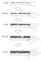
그런데, 프린트 기판의 일반적인 제조 방법으로서는, 도 13에 도시한 바와 같이, 표면에 구리 도금(133)을 행한 구리 붙임 에폭시 기판(134)에 광감광성의 레지스트(132)를 도포하고, 포토 마스크(131)를 거쳐 노광[도 13의 (a)]하고, 현상을 행하여 레지스트막에 소정의 패턴을 형성한다[도 13의 (b)]. 그 후, 레지스트로 덮이지 않은 구리 패턴부를 산으로 에칭해서[도 13의 (c)], 레지스트막을 제거하여 도체 패턴을 형성한다[도 13의 (d)].By the way, as a general manufacturing method of a printed board, as shown in FIG. 13, the
다층화를 행하는 경우는, 상술한 방법에 의해 도체 패턴이 형성된 기판을, 프리프레그(prepreg)라는 접착제를 개재하여 복수매 중첩시켜, 고온하에서 가압하여 적층 접착시킨 후, 소정의 위치에 드릴 등으로 관통 구멍을 뚫는다. 그 후, 화학 도금, 전기 도금에 의해 관통 구멍부에서 전기적으로 도통을 취하고, 포토리소그래피 공정, 에칭 공정에 의해 최외층을 형성하고 있다.In the case of multilayering, a plurality of substrates on which a conductor pattern is formed by the above-described method are superimposed via an adhesive called prepreg, pressurized at a high temperature to be laminated, and then penetrated to a predetermined position by a drill or the like. Drill a hole. Thereafter, conduction is conducted electrically in the through hole by chemical plating and electroplating, and an outermost layer is formed by a photolithography step and an etching step.
한편, 세라믹 기판의 제조 방법으로서는, 우선, 세라믹 분말과 유기 바인더를 섞어 그린 시트라는 시트를 제조한다. 이 그린 시트에 펀치 등에 의해 관통 구멍을 뚫고, 이 구멍에 도체 페이스트를 충전한 후, 마찬가지로 도체 페이스트로 시트 위에 패턴을 인쇄한다. 다시, 이러한 시트를 복수매 중첩시켜, 소결로에 의해 1000 ℃ 이상의 고온에서 소결하여 제조 하고 있다.On the other hand, as a manufacturing method of a ceramic substrate, the sheet called a green sheet is manufactured by mixing a ceramic powder and an organic binder first. Through-holes are drilled through this green sheet by a punch or the like, and the conductor paste is filled in these holes, and then similarly, the pattern is printed on the sheet with the conductor paste. In addition, a plurality of such sheets are superimposed and manufactured by sintering at a high temperature of 1000 ° C. or higher by a sintering furnace.
상술한 대로, 종래의 제조 방법에 의하면, 레지스트의 도포, 노광, 현상, 에칭 공정 등 대단히 많은 제조 공정을 거쳐 회로판이 제조되므로, 에칭 장치나 가공 접착용의 장치 등 많은 생산 설비가 필요하였다. 또한, 관통 구멍의 형성 및 관통 구멍내로의 도금 공정 등 복잡한 공정을 필요로 하므로, 고도의 제조 기술을 필요로 함과 동시에 제조 비용이 높아진다고 하는 문제가 있었다.As mentioned above, according to the conventional manufacturing method, since a circuit board is manufactured through a very large number of manufacturing processes, such as the application | coating, exposure, image development, and etching process of a resist, many production facilities, such as an etching apparatus and an apparatus for work bonding, were needed. In addition, since a complicated process such as formation of a through hole and a plating process into the through hole is required, there is a problem that a high manufacturing technique is required and a manufacturing cost increases.
본 발명의 목적은, 제조에 필요한 총 공정수를 대폭으로 감소하고, 상술한 바와 같은 복잡한 공정을 행하지 않으며, 낮은 비용으로 회로판을 제조하는 방법을 제공하는 것이다.An object of the present invention is to provide a method of manufacturing a circuit board at a low cost without significantly reducing the total number of steps required for manufacturing, and performing a complicated process as described above.
본 발명에서는, 에폭시 수지, 세라믹재, 혹은 플라스틱재 등으로 이루어지는 베이스 기판상의 원하는 부분에 도체 재료를 패턴 인쇄하고 경화시켜 제1 도체층을 형성하는 제1 공정, 제1 도체층상의 원하는 부분에 절연재를 패턴 인쇄하고 경화시켜 제1 절연층을 형성하는 제2 공정, 및 제1 도체층 및 제1 절연층상의 원하는 부분에 도체 재료를 패턴 인쇄하고 경화시켜 제2 도체층을 형성하는 제3 공정으로부터 인쇄 회로판을 제조한다. 이로써, 절연층에의 관통 구멍의 형성 및 관통 구멍에의 도금 공정이나, 가압 접착용의 설비 등 많은 생산 설비를 이용하지 않고, 간단한 공정 및 설비에 의해 인쇄 회로판을 제조할 수 있으며, 낮은 제조 비용으로 단기간에 제조가 가능해진다.In the present invention, the first step of forming a first conductor layer by pattern-printing and curing a conductor material on a desired portion on a base substrate made of an epoxy resin, a ceramic material, a plastic material, or the like, and an insulating material on a desired portion on the first conductor layer. Pattern printing and curing to form a first insulating layer, and a third step of pattern printing and curing a conductive material on the first conductor layer and a desired portion on the first insulating layer to form a second conductor layer. Manufacture a printed circuit board. Thereby, a printed circuit board can be manufactured by a simple process and installation, without using many production facilities, such as formation of a through-hole in an insulating layer, the plating process to a through-hole, and the equipment for pressure bonding, and low manufacturing cost. This enables manufacturing in a short time.
또한, 원하는 부분에 절연재를 패턴 인쇄하고 경화시켜 절연층을 형성하는 공정 및 그 절연층상의 원하는 부분에 도체 재료를 패턴 인쇄하여 경화시켜 도체층을 형성하는 공정을 복수회 반복하여, 상호간에 절연층을 개재시켜 복수층의 도체층을 형성한다. 이로써, 도체 재료가 인쇄된 기판과 절연 기판을 중첩시켜 고온하에서 가압하는 가압 접착 공정이 필요하지 않게 되어, 기판의 수축을 억제할 수 있다.Furthermore, the process of pattern-printing and hardening an insulating material in a desired part and forming an insulating layer, and the process of pattern-printing and hardening a conductor material in the desired part on this insulating layer, and forming a conductor layer are repeated several times, mutually insulating layer Multiple conductor layers are formed through this. This eliminates the need for a pressure bonding process in which the substrate on which the conductor material is printed and the insulating substrate are superposed and pressurized at a high temperature, so that shrinkage of the substrate can be suppressed.
또한, 최상면에 도체층이 형성되어 있는 기판의 원하는 부분에, 절연재를 패턴 인쇄하여 경화시켜, 절연층을 형성하고나서, 다시 그 절연층상에 도체층과 절연층의 인쇄를 반복 행하여, 배선 패턴을 형성한다. 이로써, 일반적으로 시판되고 있는 배선 기판상에 다시 배선층을 형성할 수 있으며, 보다 고밀도의 실장이 가능해진다.In addition, an insulating material is printed and cured on a desired portion of the substrate on which the conductor layer is formed on the uppermost surface to form an insulating layer. Then, the conductor layer and the insulating layer are repeatedly printed on the insulating layer to form a wiring pattern. Form. As a result, a wiring layer can be formed again on a commercially available wiring board, and higher density mounting is possible.
또한, 절연재로서 자외선 경화형 수지를 사용함으로써, 그 재료에 있던 파장의 자외선을 조사하는 것 만으로 절연재를 경화시킬 수 있으며, 단시간에 절연층을 형성할 수 있다.Moreover, by using ultraviolet curable resin as an insulating material, an insulating material can be hardened only by irradiating the ultraviolet-ray of the wavelength which existed in the material, and an insulating layer can be formed in a short time.
또한, 베이스 기판에 대하여, 전 공정에서 가해지는 가장 높은 온도 이상으로 가열하여 어닐링 처리를 행함으로써, 베이스 기판의 수축률을 현저히 저하시킬 수 있으며, 패턴 인쇄시의 마스크의 위치 정합 정밀도를 향상시킬 수 있다.In addition, by performing annealing treatment with the base substrate heated to the highest temperature or higher applied in the previous step, the shrinkage of the base substrate can be significantly reduced, and the positional alignment accuracy of the mask during pattern printing can be improved. .
본 발명의 실장 방법에 의하면, 도체층이 건조 경화하기 전에, 그 도체층상의 원하는 부분에 전자 부품을 탑재하고, 전자 부품의 전극과 도체층을 접촉시킨 상태에서 도체층을 경화시켜, 도체층을 형성함과 동시에 도체 페이스트의 고착력에 의해 도체층과 전자 부품을 접속한다. 이로써, 땜납의 공급 공정이나 리플로우 공정을 행하지 않고 전자 부품의 실장을 행할 수 있으며, 제조 공정수를 감소시키고 비용을 절감할 수 있다.According to the mounting method of this invention, before a conductor layer is dry hardened, an electronic component is mounted in the desired part on the conductor layer, the conductor layer is hardened in the state which contacted the electrode of an electronic component, and a conductor layer, At the same time, the conductor layer and the electronic component are connected by the fixing force of the conductor paste. Thereby, the electronic component can be mounted without performing the solder supply step or the reflow step, and the number of manufacturing steps can be reduced and the cost can be reduced.
또한, 절연재를 패턴 인쇄함으로써 형성되는 도체층상의 개구부에 도체 재료를 패턴 인쇄하고, 개구부를 완전히 충전하는 양 보다도 적은 양의 도체 재료를 개구부에 충전하며, 도체 재료가 경화하기 이전에, 전자 부품의 전극을 개구부에 삽입하여 개구부내에서 전극과 도체 재료를 접촉시킨 상태에서 도체 재료를 경화시켜, 도체층을 형성함과 동시에 도체층과 전자 부품의 전극을 접속한다. 이로써, 전자 부품을 더욱 얇게 실장할 수 있으며, 기판의 다층화를 도모한 경우에도 전체의 두께를 줄일 수 있다. 그리고, 종래에 비하여 고밀도로 실장할 수 있는 회로 기판을 작성할 수 있다.In addition, the conductive material is pattern-printed into the openings on the conductor layer formed by pattern printing the insulating material, and the openings are filled with a smaller amount of the conductive material than the amount to completely fill the openings. The conductor material is cured in the state where the electrode is inserted into the opening and the electrode and the conductor material are brought into contact in the opening, thereby forming a conductor layer and connecting the conductor layer and the electrode of the electronic component. Thereby, the electronic component can be mounted thinner and the overall thickness can be reduced even when the substrate is multilayered. And the circuit board which can be mounted at a high density compared with the past can be produced.
또한, 본 발명의 제조 방법을 인쇄 회로판으로서의 박형 카드에 적용할 수 있다. 이 경우, 도체 형성과 IC 칩의 접속을 동시에 행하는 실장 방법을 병용함으로써, 더욱 얇게 고밀도로 실장된 카드를 작성할 수 있다. 또한, 베이스 기판으로서 투명한 PET를 사용한 경우에는, 투명한 PET 시트의 내측 표면부터 미리 디자인 인쇄를 행하여 둠으로써, 제조된 카드의 표면에는, PET의 투명한 광택이 남고, 제조 후 카드 표면부터 인쇄를 행하였을 때와 같은 요철부도 나타나지 않으며, 도안의 색이 바래는 일도 없다.Furthermore, the manufacturing method of this invention can be applied to the thin card as a printed circuit board. In this case, by using a mounting method for simultaneously conducting conductor formation and connecting an IC chip, a card mounted in a thinner and higher density can be produced. In the case where transparent PET is used as the base substrate, design printing is performed in advance from the inner surface of the transparent PET sheet, so that the surface of the manufactured card retains the transparent gloss of PET and is printed from the surface of the card after manufacture. There is no irregularity like time, and the color of the pattern does not fade.
도 1은 본 발명의 일 실시예에 따른 인쇄 회로판의 제조 공정을 도시한 도면.1 is a view showing a manufacturing process of a printed circuit board according to an embodiment of the present invention.
도 2는 본 발명의 다른 실시예에 따른 인쇄 회로판의 단면을 도시한 도면.2 is a cross-sectional view of a printed circuit board according to another embodiment of the present invention.
도 3은 본 발명에 따른 인쇄 회로판에의 전자 부품의 일 실장례를 도시한 도면.3 is a diagram showing an example of mounting an electronic component on a printed circuit board according to the present invention.
도 4는 본 발명에 따른 인쇄 회로판에의 전자 부품의 다른 실장례를 도시한 도면.4 shows another example of mounting of electronic components on a printed circuit board according to the present invention;
도 5는 본 발명에 따른 박형(薄型) 소카드의 제조 방법의 일 실장례를 도시한 도면.Fig. 5 is a diagram showing one example of the manufacturing method of a thin socard according to the present invention.
도 6은 본 발명에 따른 박형 카드의 제조 방법의 다른 실장례를 도시한 도면.6 is a view showing another example of the manufacturing method of the thin card according to the present invention.
도 7은 본 발명의 일 실장례에 따른 박형 카드의 제조 공정을 도시한 도면.7 is a view showing a manufacturing process of a thin card according to one embodiment of the present invention.
도 8은 본 발명에 의한 박형 카드의 제조 방법의 다른 실장례를 도시한 도면.8 is a view showing another example of the manufacturing method of the thin card according to the present invention.
도 9는 전자 부품을 기판상에 실장하였을 때의 평면도.9 is a plan view when the electronic component is mounted on a substrate;
도 10은 종래의 박형 카드 제조 방법의 개요를 도시한 도면.10 is a view showing an outline of a conventional thin card manufacturing method.
도 11은 종래의 기판 제조 방법의 일 실시예를 도시한 도면.11 illustrates an embodiment of a conventional substrate manufacturing method.
도 12는 본 발명에 따른 기판 제조 방법의 일 실시예를 도시한 도면.12 illustrates an embodiment of a substrate manufacturing method according to the present invention.
도 13은 종래의 도체 패턴 인쇄 방법을 도시한 도면.Fig. 13 is a diagram showing a conventional conductor pattern printing method.
도 14는 옵셋 인쇄의 개략도.14 is a schematic diagram of offset printing.
도 15는 본 발명에 따른 박형 카드의 단면의 일 예를 도시한 도면.15 is a view showing an example of a cross section of a thin card according to the present invention.
〈도면의 주요 부분에 대한 부호의 설명〉<Explanation of symbols for main parts of drawing>
1 : 기판1: substrate
2 : 제1 도체층2: first conductor layer
3 : 제1 절연층3: first insulating layer
4 : 제2 도체층4: second conductor layer
5 : 제2 절연층5: second insulating layer
6 : 제3 도체층6: third conductor layer
다음에, 본 발명의 일 실시예를 도면을 사용하여 구체적으로 설명한다.Next, an embodiment of the present invention will be described in detail with reference to the drawings.
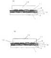
도 1은 3 층의 도체층을 갖는 인쇄 회로판을 제조하는 공정을 도시한 것이다.1 shows a process for producing a printed circuit board having three conductor layers.
도 1에서 인쇄 회로판은, 예를 들면 베이스재로서 플라스틱재를 사용한 기판(1), 제1 도체층(2), 제1 절연층(3), 제2 도체층(4), 제2 절연층(5), 제3 도체층(6)으로 구성된다.In FIG. 1, the printed circuit board is, for example, a
이 인쇄 회로판의 제조 공정을 이하에 설명한다.The manufacturing process of this printed circuit board is demonstrated below.
우선, 베이스가 되는 기판(1) 위에, 페이스트형 도체 재료를 예를 들면 스크린 인쇄법을 사용하여 패턴 인쇄하고, 제1 도체층(2)을 형성한다. 스크린 인쇄 방법으로서는, 원하는 패턴 형상에 개구부를 갖는 마스크를 씌우고, 그 위에 도체 페이스트를 공급하여, 스퀴즈(squeeze)해서 연장시키는 방법에 의해 행한다.First, the paste-type conductor material is pattern-printed using the screen printing method, for example on the board |
그 후, 기판(1)을 적외선에 의해 가열 건조시키는 노(爐)나, 열풍에 의해 건조시키는 노 등에 반송하여, 거기서 제1 도체층(2)을 건조·경화시킨다.Thereafter, the
다음에, 제1 도체층(2)이 형성된 기판상에 원하는 패턴 형상의 개구부를 갖는 마스크를 씌우고, 그 위에 페이스트형의 절연 재료를 공급해서 스퀴즈하여 연장시키고, 제1 도체층(2) 및 기판(1) 위에 패턴 인쇄하여, 제1 절연층(3)을 형성한다. 그 때, 제1 도체층과 제2 도체층이 전기적으로 접속되도록, 제1 절연층(3)의 원하는 부분에 개구부가 되는 영역(22)을 형성할 필요가 있다. 그 후, 제1 절연층(3)을 건조에 의해 경화시킨다.Next, a mask having an opening having a desired pattern shape is covered on the substrate on which the
다시, 제1 도체층(2)의 형성과 마찬가지의 방법에 의해, 제2 도체층(4)을 패턴 인쇄에 의해 형성하여 경화시킨다. 이 때, 상기 제1 도체층(2)과 제2 도체층(4)은 제1 절연층(3)에 의해 전기적으로 절연되지만, 제1 도체층(2) 위의 절연 재료가 도포되지 않았던 영역(2)에는, 제2 도체층(4)의 패턴 인쇄시에 페이스트형의 도체 재료가 흘러, 패스부를 형성하여 제1 도체층(2)과 제2 도체층(4)이 전기적으로 접속되게 된다.Again, the
다시, 상기와 마찬가지의 공정을 반복하여 제2 도체층(4)상에 제2 절연층(5)을 형성하고, 그 위에 제3 도체층(6)을 형성한다. 이로써 3 층의 도체층을 갖는 인쇄 회로판을 제조할 수 있다.Again, the same process as above is repeated, the 2nd insulating
페이스트형의 도체 재료로서는, 통상, 구리나 은 등의 금속 미세분에 에폭시 수지나, 메라민, 아크릴계의 열경화성 수지, 열가소성 수지가 섞인 것 등을 사용할 수 있다.As a paste-type conductor material, what mixed the metal fine powders, such as copper and silver, with an epoxy resin, a melamine, an acryl-type thermosetting resin, and a thermoplastic resin can be used normally.
또한, 절연 재료로서는, 에폭시계의 수지나, 이들 유기 재료에 알루미나분 등의 세라믹 재료를 혼합한 것, 혹은 자외선 경화형의 수지 등을 사용할 수 있다.Moreover, as an insulating material, what mix | blends ceramic materials, such as an alumina powder, with epoxy resin, these organic materials, ultraviolet curable resin, etc. can be used.
도체 페이스트나 절연재 페이스트에 의한 패턴 형성은 상기와 같이 마스크를 개재하는 인쇄에 의해 행한다. 인쇄 마스크로서는, 도체층의 인쇄 및 절연층의 인쇄 모두, 종래부터 일반적으로 이용되고 있는 폴리에스테르의 메시에 에멀전에 의해 패턴을 형성한 것이나, 메탈 마스크 등, 용도에 따라 여러 가지를 사용할 수 있다.Pattern formation by a conductor paste or an insulating material paste is performed by printing through a mask as above. As a printing mask, both the printing of a conductor layer and the printing of an insulating layer can use various things according to the use, such as the thing which formed the pattern by emulsion in the mesh of polyester generally used conventionally, and a metal mask.
인쇄된 도체 재료나 절연재의 경화는, 통상, 건조에 의해 경화시키는 것이 일반적이다. 단, 상술한 바와 같은 자외선 경화형의 수지(레지스트)를 페이스트로서 선정하면, 재료에 맞는 파장의 자외선을 조사함으로써, 단시간에 경화시킬 수 있게 된다.It is common to harden | cure the printed conductor material and insulating material by drying normally. However, when the above-mentioned ultraviolet curable resin (resist) is selected as a paste, it can be cured in a short time by irradiating ultraviolet rays having a wavelength suitable for the material.
종래의 기판 제조 방법과 본 발명에 의한 기판 제조 방법에 대하여, 전 공정수를 도 11 및 도 12를 이용하여 비교한다. 도 11은 종래의 제조 공정의 일 예를, 도 12는 본 발명에 의한 제조 공정을 도시하고 있다. 각 공정에 대한 상세한 설명은 생략하지만, 도 11에 도시한 바와 같이 종래의 제조 방법에서는 전 39 공정이 필요하였으나, 본 발명의 제조 방법에 의하면 도 12에 도시한 바와 같이 전 12 공정으로 기판을 제조할 수 있게 되며, 제조 공정수가 대폭으로 감소하므로, 시간도 제조 비용도 절감할 수 있다.With respect to the conventional substrate manufacturing method and the substrate manufacturing method according to the present invention, the total number of steps is compared using Figs. 11 and 12. 11 shows an example of a conventional manufacturing process, and FIG. 12 shows a manufacturing process according to the present invention. Although a detailed description of each process is omitted, as shown in FIG. 11, all 39 processes are required in the conventional manufacturing method, but according to the manufacturing method of the present invention, the substrate is manufactured in all 12 processes as shown in FIG. The number of manufacturing processes can be greatly reduced, thereby saving time and manufacturing costs.
또한, 종래의 제조 방법에서는 각각의 공정에 관하여 제조 설비가 필요하였으나, 본 발명에 의하면 인쇄 설비와 건조 설비가 있으면, 기판을 작성할 수 있다. 따라서, 제조 설비가 적어지므로, 설비 비용도 절감할 수 있다.In addition, in the conventional manufacturing method, a manufacturing facility is required for each step, but according to the present invention, a substrate can be prepared if there is a printing facility and a drying facility. As a result, fewer manufacturing facilities can reduce the installation cost.
본 실시예에서는 도체층의 수는 3 층인 것에 대하여 설명하였으나, 상술한 도체 인쇄 공정과 절연재 인쇄 공정을 반복하여 실시함으로써, 임의의 도체층의 수를 갖는 인쇄 회로판을 제조할 수 있게 된다. 즉, 종래 기술에서 설명한 바와 같은, 절연층에 구멍을 뚫는 공정, 구멍에 페이스트를 충전하는 공정 및 적층 프레스 공정은 필요하지 않으며, 단지 도체와 절연재의 인쇄 공정을 반복하는 것 만으로, 간단히 적층 회로판을 형성할 수 있다.In the present embodiment, the number of the conductor layers has been described as three layers, but by repeating the above-described conductor printing process and the insulating material printing process, a printed circuit board having an arbitrary number of conductor layers can be manufactured. That is, as described in the prior art, a process of punching an insulating layer, a process of filling paste into a hole, and a lamination press process are not necessary, and simply repeating the printing process of a conductor and an insulation material, the laminated circuit board is simply formed. Can be formed.
또한, 본 발명의 제조 방법을 사용하면, 널리 일반적으로 사용되고 있는 프린트 기판이나, 세라믹 기판을 베이스 기판으로서 사용하고, 또한, 이 기판상에 도 1에 도시한 바와 같이 도체층 및 절연층을 적층하여 형성함으로서, 보다 부가가치가 높은 인쇄 회로판을 용이하고 저렴하게 제조할 수 있다.In addition, if the manufacturing method of the present invention is used, a printed substrate or a ceramic substrate which is widely used is used as a base substrate, and a conductor layer and an insulating layer are laminated on this substrate as shown in FIG. By forming, a printed circuit board with higher added value can be manufactured easily and inexpensively.
이러한 실시예에 대하여 도 2에 도시한다. 도 2에서 도 1에 도시한 부분과 동일한 부분에 대해서는 동일 부호를 부여하고 있다.This embodiment is shown in FIG. In FIG. 2, the same code | symbol is attached | subjected about the part same as the part shown in FIG.
도 2에서, 베이스 기판은, 상술한 바와 같은 종래 방법으로 제조한 일반적으로 널리 사용되고 있는 세라믹 기판을 사용하며 세라믹 베이스(7), 세라믹 베이스(7)내에 형성된 도체층(8), 세라믹 베이스(7)에 설치된 외부 인터페이스용 핀(9)으로 구성된다.In Fig. 2, the base substrate is a
베이스 기판의 도체층(8) 위에 페이스트형의 도체 재료를 패턴 인쇄하여 제1 도체층(2)을 형성하고, 베이스 기판의 도체층(8)의 전기적 도통을 확보한다. 그 후, 도 1에 도시한 공정에 의해 절연층과 도체층을 교대로 형성하여 경화시킴으로써, 일반적으로 사용되고 있는 인쇄 회로판상에, 다시 도체층을 적층하여 다층화할 수 있게 된다.The
베이스 기판으로서는, 유리 에폭시 수지 등의 유기 재료를 사용한 프린트 기판도 적용할 수 있다.As a base substrate, the printed circuit board which used organic materials, such as glass epoxy resin, is also applicable.
또한, 필요에 따라서는 베이스 기판 위에 우선 절연재를 패턴 인쇄하여 경화시킨 후, 마찬가지의 방법으로 인쇄 회로판을 제조할 수도 있다.In addition, if necessary, the insulating material may be first printed on the base substrate by pattern printing, and then a printed circuit board may be manufactured by the same method.
다음에, 본 발명의 제조 방법에 의해 제조된 인쇄 회로판에 LSI 등의 전자 부품을 실장하는 경우의 실장례를 도 3을 사용하여 구체적으로 설명한다.Next, the example of mounting in the case of mounting an electronic component, such as LSI, on the printed circuit board manufactured by the manufacturing method of this invention is demonstrated concretely using FIG.
도 3에서, 도면 부호 10은 LSI 등의 전자 부품, 11은 전자 부품 전극을 나타내며, 12는 언더 필(under fill)용 접착제를 도시한다.In FIG. 3,
도 3의 (a)에 도시한 바와 같이 전자 부품(10)을 인쇄 회로판에 실장하기 위해서는, 우선, 도 1에 도시한 공정에 의해 인쇄 회로판을 제조하고, 제3 도체층(6)을 패턴 인쇄한다. 그 직후, 이 도체 재료가 경화되기 이전에, 전자 부품(10)을 제3 도체층(6) 위의 탑재 위치에 탑재한다. 이때, 전자 부품(10)은 경화 전의 도체층의 점착성(粘着性)에 의해 제3 도체층(6) 위에 유지된다. 그리고, 전자 부품의 전극(11)과 제3 도체층(6)의 접속 개소(箇所)를 접촉시킨 상태에서, 제3 도체층(6)을 건조하여 경화시킨다.In order to mount the
이 경화시의 도체 재료의 고착력에 의하여, 전자 부품과 도체층을 전기적 도통을 유지하면서, 약 200 gf의 힘으로 수직으로 잡아당겨도 떨어지지 않을 정도의 기계적 유지력으로 전자 부품과 도체층을 직접 접속할 수 있어, 전자 부품(10)을 인쇄 회로판에 확실히 실장할 수 있다.Due to the fixing force of the conductor material at the time of curing, the electronic component and the conductor layer can be directly connected with a mechanical holding force that does not drop even when the electronic component and the conductor layer are pulled vertically with a force of about 200 gf while maintaining electrical conduction. The
제3 도체층(6)에 전자 부품을 직접 접속하기 위하여, 종래 필요하였던 땜납 공급 공정, 플럭스(flux)의 도포 공정 및 땜납 건조 공정이 필요하지 않게 되어, 공정수의 감소 및 시간의 단축을 도모할 수 있다.In order to directly connect the electronic component to the
또한, 필요에 따라, 도 3의 (b)에 도시한 바와 같이 전자 부품(10)의 하면에 언더 필 접착제(12)를 충전하여 경화시킴으로써, 전자 부품과 도체층의 기계적 유지력을 보강할 수도 있다.If necessary, as shown in FIG. 3B, the
도 4를 참조하여 전자 부품의 다른 실장례에 대하여 설명한다.With reference to FIG. 4, the other mounting example of an electronic component is demonstrated.
본 실시예에서는, 전자 부품의 전극(11)과 인쇄 회로판의 제3 도체층(6)간에, 땜납 혹은 도전성 접착제 등의 접합 재료(16)를 공급하여, 전자 부품(10)과 제3 도체층(6)을 접속한다. 즉, 도 1에 도시한 공정에 의하여 제3 도체층(6) 까지를 패턴 인쇄하여 건조 경화시켜, 인쇄 회로판을 완성시킨다. 그 후, 제3 도체층(6)상의 전자 부품 탑재 위치에 땜납 등의 접합 재료(16)를 인쇄 등에 의해 공급한다. 그리고, 공급된 접합 재료(16)를 개재하여 제3 도체층(6) 위에 전자 부품(10)을 탑재하고, 그 상태에서 인쇄 회로판을 가열하여 접합 재료를 녹임으로써 전자 부품과 인쇄 회로판을 접속한다.In this embodiment, the
또한, 인쇄 회로판과 그것에 실장되는 전자 부품과는, 접속 신뢰성을 확보하기 위하여, 동일한 열팽창율을 갖는 것을 조합시킬 필요가 있다. 단, 상술한 바와 같은 인쇄 회로판의 제조 방법에 의하면, 인쇄 회로판의 열팽창율은 베이스 기판의 재료에 의해 거의 결정할 수 있으며, 게다가 베이스 기판의 베이스재로서 어떠한 재료를 선정하는지는 자유이다. 따라서, 탑재할 전자 부품이 예를 들어 세라믹스에 의해 형성되어 있는 경우에는, 베이스 기판으로서 세라믹 기판을 선정하면 된다. 또한, 탑재 부품의 열팽창율이 금속에 가까운 경우에는 금속판을 베이스 기판으로서 선정할 수 있다. 이 경우는 베이스 기판 위에 우선 절연 페이스트를 인쇄하여 경화시킨 후, 상술한 바와 같은 방법으로 인쇄 회로판을 제조한다.Moreover, in order to ensure connection reliability, it is necessary to combine the printed circuit board and the electronic component mounted in it with the thing with the same coefficient of thermal expansion. However, according to the manufacturing method of the printed circuit board mentioned above, the thermal expansion coefficient of a printed circuit board can be almost determined by the material of a base board, and what kind of material is selected as a base material of a base board. Therefore, what is necessary is just to select a ceramic substrate as a base substrate, when the electronic component to be mounted is formed by the ceramics, for example. In addition, when the thermal expansion coefficient of a mounting component is close to metal, a metal plate can be selected as a base substrate. In this case, the insulating paste is first printed and cured on the base substrate, and then a printed circuit board is manufactured by the method as described above.
또한, 상술한 땜납 등 대신에 이방성 도전막을 접합 재료로서 이용함으로써, 전자 부품(10)과 제3 도체층(6)을 접속할 수도 있다. 이 경우, 전자 부품의 전극(11)과 제3 도체층(6)간에 이방성 도전막을 공급하여, 양자를 가압하면서 가열하여 접속한다.In addition, the
다음에, 본 발명의 제조 방법을 IC 카드 등의 전자 부품을 탑재한 박형 카드에 적용한 경우에 대하여 도 5, 도 7 및 도 10을 사용하여 설명한다.Next, the case where the manufacturing method of the present invention is applied to a thin card on which electronic components such as an IC card is mounted will be described with reference to FIGS. 5, 7 and 10.
먼저, 종래의 박형 카드의 제조 방법에 대하여, 도 10을 참조하여 설명한다.First, the manufacturing method of the conventional thin card is demonstrated with reference to FIG.
도 10에서, 도면 부호 101은 리드 코일, 102는 회로 칩, 103은 기판, 104는 접착제, 105 및 106은 폴리 염화 비닐(이하, ″PVC″라 함)을 도시하고 있다.In Fig. 10, reference numeral 101 denotes a lead coil, 102 a circuit chip, 103 a substrate, 104 an adhesive, 105 and 106 polyvinyl chloride (hereinafter referred to as "PVC").
리드 코일(101)과 회로 칩(102)을 프린트 기판(103)에 납땜 부착 또는 열압착 접합한다. 다음에, PVC(105) 재료에 원하는 형상의 오목부를 형성하고, 접착제(104)를 사용하여, 리드 코일(101)과 회로 칩(102)이 전기적 접합을 확보한 상태에서 PVC(105) 위에 고정한다. 그 후, 상면 커버용 PVC(106)를 초음파 가공이나 그 외의 공법으로 가열 융착한다.The lead coil 101 and the circuit chip 102 are soldered or thermocompression-bonded to the printed board 103. Next, recesses having a desired shape are formed in the PVC 105 material, and the adhesive 104 is used to fix the PVC 105 on the PVC 105 in a state in which the lead coil 101 and the circuit chip 102 have secured electrical bonding. do. Thereafter, the top cover PVC 106 is heat-sealed by ultrasonic processing or other methods.
이 때, 리드 코일(101) 접합시나 회로 칩(102) 접합시에, 주석/납 공정(共晶) 납땜(융점 183 ℃)을 사용하거나 하면, 융점 이상의 가열을 행할 필요성에서 180 ℃ 이상의 히터 가열봉을 사용하지 않으면 안되었다. 또한, 회로 칩의 접합에 이방성 도전막을 사용하는 경우에서도, 가열 압착 히터로서 약 180 ℃ 이상의 히터가 필요하였다.At this time, when the lead coil 101 is bonded or the circuit chip 102 is bonded, if a tin / lead soldering process (melting point of 183 ° C) is used, a heater heating of 180 ° C or more is required in order to perform heating above the melting point. I had to use a rod. In addition, even when an anisotropic conductive film was used for joining the circuit chips, a heater of about 180 ° C. or more was required as the heat-compression heater.
다음에, 본 발명에 의한 박형 카드의 제조 방법을 도 5 및 도 7을 참조하여 설명한다.Next, the manufacturing method of the thin card according to the present invention will be described with reference to FIGS. 5 and 7.
도 5에서, 도면 부호 201은 전술한 베이스가 되는 기판으로서, 가요성 기판이며, 여기서는 PET(폴리에틸렌텔레프탈레이트)이다. 202는 제1 도체층, 203은 절연층, 204는 제2 도체층, 211은 회로 칩 단자(전자 부품 전극), 210은 회로 칩(전자 부품), 217은 점착제, 212는 표면에 라미네이트된 시트형 PET를 도시하고 있다.In FIG. 5,
도 7은 상기 실시예의 제조 방법의 흐름도를 도시한 것이다. 701은 가열 처리(어닐링 처리) 공정, 702는 제1 도체층의 인쇄 공정, 703은 건조 공정, 704는 절연층의 인쇄 및 경화 건조 공정, 705는 제2 도체층의 인쇄 공정, 706은 회로 칩 탑재 공정, 707은 접합·건조 공정, 708은 점착제(217)가 부착된 PET(212)에 의한 라미네이트 공정, 709는 디자인 인쇄 공정, 710은 절단·분할 공정을 도시하고 있다.7 shows a flowchart of the manufacturing method of the above embodiment. 701 is a heat treatment (annealing) process, 702 is a printing process of the first conductor layer, 703 is a drying process, 704 is a printing and curing drying process of the insulating layer, 705 is a printing process of the second conductor layer, and 706 is a circuit chip The mounting process, 707 shows a bonding and drying process, 708 shows a lamination process by
우선, 먼저 도 5의 (b)에 도시한 바와 같이, PET(201) 위에 Ag로 이루어지는 제1 도체층(202)을 형성한다. 도체층의 형성은 일반적으로 이용되는 도체 패턴 인쇄 방법을 이용하여 행한다. 인쇄 방법으로서는, 예를 들면, 원하는 패턴 형상으로 개구부를 갖는 마스크를 씌우고, 그 위에 도체 페이스트를 공급하여, 스퀴즈해서 연장시키는 스크린 인쇄 방법에 의해 행한다[제1 도체층의 인쇄 공정(702)].First, as shown in FIG. 5B, a
다음에, 형성된 제1 도체층(202)을 갖는 PET1을 노 안에 두고, 150 ℃로 약 5 분간 가열하고, 건조시킨다[건조 공정(703)].Next, PET1 having the formed
제1 도체층(202)이 건조되면, 도 5의 (c)에 도시한 바와 같이, 이번에는 제1 도체층(202) 및 PET(201)상에, 페이스트형의 절연재를, 도체층과 마찬가지로, 예를 들어 스크린 인쇄법을 이용해서 패턴 인쇄하여, 제1 도체층(202) 위에 절연층(203)을 형성한다. 이때, 절연층(203) 위에 형성되는 제2 도체층(204)과 제1 도체층(202)을 전기적으로 접속시킴으로써, 미리 절연층(203)에 접속용 개구부(222)가 형성되게 패터닝해 둔다.When the
인쇄된 절연층(203)의 경화는, 통상, 건조에 의해 경화시키는 것이 일반적이지만, 절연재로서 자외선 경화형의 수지(레지스트) 등을 이용한 경우는, 재료에 맞는 파장의 자외선을 조사함으로써, 단시간에 경화시킬 수 있다[절연층의 인쇄 및 경화 건조 공정(704)].Although the hardening of the printed insulating
다음에, 도 5의 (d)에 도시한 바와 같이, 제2 도체층(204)을 절연층(203) 위에 패턴 인쇄한다[제2 도체층의 인쇄 공정(705)]. 이때, 절연층(203)에 미리 형성해 둔 접속용 개구부(222)에 도체가 인쇄되며, 제1 도체층(202)과 제2 도체층(204)이 전기적으로 접속된 상태가 된다.Next, as shown in Fig. 5D, the
제2 도체층(204)이 경화하기 전에, 도 5의 (e)에 도시한 바와 같이, 전자 부품(210)을 인쇄 패턴에 맞게 배치하고, 회로 칩(210)의 회로 칩 단자(211)(예를 들면, Au 15 ㎛ 두께)를 제2 도체층(204)에 접속시킨다[회로 칩 탑재 공정(706)].Before the
회로 칩(210)을 제2 도체층(204)에 탑재한 상태를 도시한 평면도를 도 9에 도시한다. 도 9의 (a)는 회로 칩 탑재 전의 모양을, 도 9의 (b)는 회로 칩을 탑재한 상태를 도시하고 있다.9 is a plan view showing a state in which the
도 9의 (a)의 회로 칩 탑재 위치에 설치되어 있는 회로 칩 단자 접속용 랜드에, 회로 칩의 복수의 단자 각각이 접속되도록 위치 정합을 행하고, 제2 도체층(204) 위에 단자를 탑재한다. 이때, 회로 칩은 건조되어 있지 않은 도체 페이스트의 점착력에 의해 PET(201) 위에 유지된다.Position matching is performed so that each of the several terminal of a circuit chip may be connected to the circuit chip terminal connection land provided in the circuit chip mounting position of FIG. 9 (a), and a terminal is mounted on the
그 후, 반송 가속도를 1 G 이하의 진동으로 억제하여 건조로(乾燥路)에 반송하여, 전체를 노 안에 넣고, 150 ℃로 약 5 분간 가열하고, 단자의 접착과 도체의 패턴의 건조를 동시에 행한다[접합·건조 공정(707)].Thereafter, the conveyance acceleration is suppressed by a vibration of 1 G or less and conveyed to a drying furnace, and the whole is put in a furnace, heated at 150 ° C. for about 5 minutes, and the adhesion of the terminal and drying of the pattern of the conductor are simultaneously carried out. [Bonding and drying step (707)].
이어서, 도 5의 (f)에 도시한 바와 같이, 접착제(217)를 표면에 도포하고, 최상면을 얇은 시트 형태의 PET(212)로 피복해서 약 120℃로 가열 롤을 행하여 라미네이트한다[라미네이트 공정(708)].Subsequently, as shown in Fig. 5 (f), the adhesive 217 is applied to the surface, and the uppermost surface is covered with a thin sheet of
최후에, 제조한 박형 카드에 옵셋 인쇄나 스크린 인쇄에 의해서 도안을 인쇄한다[디자인 인쇄 공정(709)].Finally, the pattern is printed on the manufactured thin card by offset printing or screen printing (design printing process 709).
본 제조 방법에 의해서 형성된 카드는 상당히 박형이고 유연성이 있으므로, 옵셋 인쇄나 스크린 인쇄를 행해도 회로 칩(210)의 깨짐이나 접속 절단이 발생되지 않고, 용지와 동일한 인쇄 등이 가능하게 된다. 예를 들면, 플라스틱 등에도 사용할 수 있는 유성 잉크를 사용한 옵셋 인쇄기에 용지와 동일하게 카드들 셋트하여 인쇄를 하거나, 마스크가 될 스크린을 통해서 유성 잉크를 인쇄할 수도 있다.Since the card formed by the present manufacturing method is considerably thin and flexible, even if offset printing or screen printing is performed, cracking or disconnection of the
또, 카드를 형성하기 전에 베이스가 될 PET 시트 또는 라미네이트되는 PET 시트에 도안을 인쇄해 둘 수도 있다. 카드 형성 후의 인쇄에서는, 카드 내에 도체 배선 및 회로 칩이 탑재되어 있으므로, 예를 들면 회로 칩의 두께가 두꺼운 경우 등은, 회로 칩에 만곡 응력이 걸리고, 균열이 발생할 경우가 있다. 이 때문에, 회로 칩 등 만곡 응력에 약한 부품을 탑재할 필요가 있는 경우에는, 미리 도안 인쇄를 실시해 두는 것이 유효한 수단이다. 또, 투명한 PET 시트의 경우에는 PET 시트의 회로 실장 측의 면으로부터 인쇄를 실시해 둠으로써, 제조된 카드의 표면에는 PET의 투명한 광택이 잔재하여, 표면으로부터 인쇄를 실시한 때와 같은 요철도 나타나지 않아서 도안의 색이 바래지는 일도 없다.In addition, a pattern may be printed on a PET sheet to be a base or a laminated PET sheet before forming a card. In printing after card formation, since the conductor wiring and the circuit chip are mounted in the card, for example, when the thickness of the circuit chip is thick, a bending stress is applied to the circuit chip, and cracks may occur. For this reason, when it is necessary to mount a component which is weak in bending stress, such as a circuit chip, it is an effective means to print a pattern beforehand. In the case of the transparent PET sheet, printing is performed from the surface of the circuit mounting side of the PET sheet, so that the transparent gloss of PET remains on the surface of the manufactured card, and the same irregularities as when printed from the surface do not appear. Color does not fade.
또, 도 7에서의 공정의 최초에, 도 5의 (a)에 도시한 베이스가 될 PET(201)를 도 7의 전 공정에 가해지는 가장 높은 온도 이상의 온도에서, 가열 처리(어닐링 처리)(701)를 해 두면, PET(201)의 열 수축률을 현저하게 저하시킬 수 있다.At the beginning of the process in FIG. 7, the
예를 들면, PET(201)를 사전에 160℃로 5 분간 어닐링 처리한 후, 150℃로 5 분간 가열하는 경우와, PET(201)에 어닐링 처리를 실시하지 않고 150 ℃로 5 분간 가열하는 경우의 열 수축률은 각각 0.03 %, 0.5 %로 되고, 1 자릿수 이상 다르게 된다.For example, after annealing the
즉, 미리 PET(201)에 어닐링 처리를 실시해서 열 수축을 억제하므로써, 패턴 인쇄를 복수회 실시하는 경우에 패턴 인쇄시의 마스크의 위치 정합 정밀도를 향상시킬 수 있고, 고품위의 카드를 제조할 수 있다.That is, by annealing the
도 6을 참조하여 박형 카드의 다른 제조 방법을 설명한다.Another manufacturing method of the thin card will be described with reference to FIG. 6.
제조 공정은 상술한 도 5 및 도 7을 참조하여 설명한 것과 거의 동일하지만, 제2 도체층(204)을 형성할 때에, 도 6의 (d)에 도시한 바와 같이, 절연층에 형성된 접속용의 개구부(222)를 완전히 도체 페이스트로 매워 버리는 것이 아니라, 상부에 도체 페이스트가 충전되지 않은 부분이 잔재하도록 제2 도체층(204)을 형성한다. 그리고, 회로 칩 단자(211)를 개구부(222)의 도체 페이스트가 충전되어 있지 않은 부분에 삽입한다. 따라서, 회로 칩 단자(211)는 개구부(222) 내에서, 제2 도체층(204)과 전기적으로 접속된 상태로 되기 때문에, 도 6의 (f)와 같이 절연층(203)과 회로 칩(210) 간에 공간이 없게 되어 한층 얇은 구조로 할 수 있다.Although the manufacturing process is substantially the same as that described with reference to FIGS. 5 and 7 described above, when forming the
또, 종래에 문제가 되고 있었던 작은 직경의 구멍[여기서는 절연층(203)의 개구부(222)]에의 도체 페이스트의 충전이 충분히 행하는데 어려움이 있는 점에 대해서도 본 발명은 효과를 발휘한다. 즉, 개구부(222)로의 도체 페이스트의 충전이 불충분하다고 해도 회로 칩 단자(211)가 개구부(222) 속으로 들어가고, 또한 개구부(222) 내부의 건조 전의 물렁물렁한 도체 페이스트가 나머지의 극간을 메우는 상태가 되어, 회로 칩 단자(211)와 도체 페이스트와의 사이에 양호한 접속 상태가 얻어진다. 이에 따라서, 작은 직경의 구멍 내로의 도체 페이스트의 불충분한 충전에 의한 단선과 같은 문제도 방지할 수 있다.In addition, the present invention also has an effect in that it is difficult to sufficiently fill the conductor paste into a small diameter hole (here, the
여기서, 본 실시예에서 사용한 PET의 두께는 80∼100㎛, Ag 페이스트의 두께는 10∼20㎛, 절연층(3)의 두께는 20∼40㎛, 회로 칩(10)의 두께는 50㎛, 점착제 층의 가장 두꺼운 부분의 두께는 50∼140㎛이다. 이로부터, 제조될 카드의 두께는 도 15에 도시한 바와 같이, PET의 두께와 점착제 층의 가장 두꺼운 부분의 두께로 정해져, 0.34㎜ 이하로 하는 것이 가능하다. 예를 들면, PET 두께를 100㎛, 회로 칩 두께를 50㎛로 하고, 점착제 층의 가장 두꺼운 부분의 두께가 100㎛가 되도록 Ag 페이스트 및 절연층의 두께를 취하므로써, 0.3㎜의 카드를 작성할 수 있다. 또, PET 두께를 80㎛로 하고, 점착제 층의 가장 두꺼운 부분의 두께가 90㎛가 되도록 Ag 페이스트 및 절연층의 두께를 취하므로써(예를 들면, Ag 페이스트 두께를 10㎛, 절연층의 두께를 20㎛로 한다), 0.25㎜의 카드를 작성할 수도 있다. 사용할 회로 칩으로서는 제조된 카드를 옵셋 인쇄기 등의 인쇄에 걸리는 정도의 유연성을 갖게 하기 위해서 100㎛ 이하의 두께의 것을 사용하는 것이 바람직하다.Here, the thickness of PET used in this embodiment is 80 to 100 µm, the thickness of the Ag paste is 10 to 20 µm, the thickness of the insulating
또한, 옵셋 인쇄기는, 판동(版胴), 고무동 및 압동의 3개의 실린더를 구비하고, 판동의 주위에 감겨 붙여진 인판에 축축한 물이나 잉크가 부착되고, 이 잉크가 고무동에 전사된 후, 고무동과 압동과의 사이를 통과하는 피인쇄물에 인쇄된다. 이 때문에, 옵셋 인쇄기를 사용한 인쇄에서는, 도 14에 도시한 바와 같이 카드가 복수의 롤러 사이를 뚫고 나가는 상태로 이송되므로, 그 인쇄 공정에서 회로 칩이 깨지지 않는 조건이 필요하며, 또 카드 자체도 인쇄기에 걸리는 범위의 두께 또한 유연성을 갖추고 있지 않으면 안된다. 본 제조 방법으로 제조된 카드는 그 두께를 0.3㎜ 이하로 억제할 수 있고, 인쇄에 견딜 수 있는 만큼의 유연성을 갖추고 있으므로, 용지와 같이 인쇄하는 것이 가능하게 된다.In addition, the offset printing machine is provided with three cylinders of a plate cylinder, a rubber tube, and a pressure plate, and wet water or ink is attached to the platen wound around the plate tube, and after the ink is transferred to the rubber tube, It is printed on a to-be-printed object which passes between rubber and pressure. For this reason, in printing using an offset printing machine, as shown in Fig. 14, since the card is conveyed in a state of penetrating between a plurality of rollers, the condition that the circuit chip is not broken in the printing process is required, and the card itself is also a printing machine. The thickness in the range must also be flexible. Since the card manufactured by this manufacturing method can suppress the thickness to 0.3 mm or less, and has the flexibility to withstand printing, it becomes possible to print like a paper.
또, 절연재 페이스트로서는 도체층이 될 도체 페이스트와의 접합성이 좋은 재료를 사용하는 것이 바람직하다.As the insulating material paste, it is preferable to use a material having good bonding property with the conductor paste to be the conductor layer.
본 실시예에서, 예를 들면, 명함 크기의 카드를 양산하고자 하는 경우에는 베이스가 될 PET로서 1m×1m 등의 크기의 것을 준비해서, PET 전면에 걸쳐서 패턴 인쇄에 의해 동일한 도체 패턴을 복수 인쇄한다. 그 위에 절연층을 인쇄하고, 다시 도체층을 인쇄하다. 상부 도체층의 소정 위치의 각각에 회로 칩을 탑재하여 PET 시트를 라미네이트한 후, 디자인 인쇄 등을 일괄적으로 행한다. 그 후에, PET를 명함 크기(54㎜×85.6㎜)로 분할하는 방법을 사용하여 효율좋게 카드를 양산할 수 있다[도 7의 절단·분할 공정(710)].In this embodiment, for example, when mass-producing a card of business card size, a PET having a size of 1m × 1m or the like is prepared as a base, and a plurality of identical conductor patterns are printed by pattern printing over the entire PET surface. . The insulating layer is printed thereon, and the conductor layer is printed again. The circuit chip is mounted at each of the predetermined positions of the upper conductor layer to laminate the PET sheet, and then design printing and the like are collectively performed. Thereafter, the card can be mass-produced efficiently by using a method of dividing PET into business card sizes (54 mm x 85.6 mm) (cutting / dividing
디자인 인쇄 공정(709)은 생략할 수도 있으며, 절단·분할 공정(710)의 후에 행할 수도 있다. 카드 형태로 형성된 후의 디자인 인쇄라면, 개인의 인쇄기 등(예를 들면, 퍼스널 컴퓨터에 접속된 프린터)으로도 인쇄할 수 있고, 자유롭게 좋아하는 도안을 인쇄할 수도 있다.The
또, 투명한 PET 시트를 이용하면, 제조 공정의 도중에 접속부의 체크를 행할 수 있고, 게다가 전자 부품 탑재시에 직접 베이스가 될 PET 측으로부터 YAG 레이저 등을 조사해서 전자 부품 단자와 도체층을 접속하기 위한 땜납재를 용해하여 단자와 도체층을 접속하는 것도 가능하다.In addition, when the transparent PET sheet is used, the connection part can be checked in the middle of the manufacturing process, and furthermore, a YAG laser or the like is irradiated from the PET side, which will be the base when the electronic component is mounted, to connect the electronic component terminal to the conductor layer. It is also possible to dissolve the solder material and connect the terminal and the conductor layer.
또, 본 실시예에서는 점착제(217)를 사용하고 있으나, 이것은 보통의 경화형 접착제와 같이 완전하게 경화해 버리는 것을 피하고, 라미네이트 후에 탄성을 갖게 하여, 접속부를 보호하기 위함이며, 동일한 효과를 얻을 수 있는 것이라면 어느 것도 대용이 가능하다.In addition, although the adhesive 217 is used in this embodiment, this is to avoid hardening completely like a normal curable adhesive, to give elasticity after lamination, and to protect a connection part, and the same effect can be acquired. Anything can be substituted.
또, 본 실시예에서는 라미네이트 공정(708)에서, 점착제(217)를 기판 표면에 도포한 후 최상면을 PET(212)로 피복하여 가열 롤을 행하여 라미네이트하는 방법을 예시하고 있다.In the present embodiment, the
그러나, 미리 점착제(17)가 도포된 PET(213)를 기판의 표면에 가열 롤해서 라미네이트하는 방법도 가능하다.However, a method of heating and laminating the PET 213 to which the pressure-sensitive adhesive 17 is applied in advance to the surface of the substrate is also possible.
또한, 본 실시예에서는, 도체 페이스트로서 Ag를 사용했으나, Ag 이외에도 구리 등, 전기 도전성을 갖고 있는 것이라면 어떤 재료라도 적용 가능하다.In addition, although Ag was used as a conductor paste in this Example, as long as it has electrical conductivity, such as copper, in addition to Ag, any material is applicable.
도 8은 이용하며, 더욱 박형의 카드를 형성하기 위한 도체층의 제조 방법의 일례에 대해서 설명한다.8, an example of the manufacturing method of the conductor layer for forming a thinner card is demonstrated.
베이스 기판인 PET(201)에 대해서, 레이저(220)를 배선 패턴 형상(219)를 그리도록 조사한다. 레이저(220)가 조사된 PET(201)는 배선 패턴 형상으로 홈이 형성되고 그 부위는 활성화된 상태로 된다. 그 후, PET(201)를 도금액으로 침적해서 활성화된 부위에 도체층(221)을 석출시킨다.On the
도 8의 (b)에 도시된 바와 같이, PET(201)의 레이저에 의해 활성화된 부분에 도체층(221)이 형성되므로, PET(201) 표면 상에 도체층(221)이 부풀어올라 인쇄되는 것이 아니라, PET(201) 표면과 동일한 높이로 형성되고, 카드 전체로 볼 때 도 5에 도시된 실시예와 비교해서 제1 도체층(2)의 두께분만큼 얇은 구조로 할 수 있다.As shown in (b) of FIG. 8, since the
본 발명에 의하면, 고밀도의 인쇄 회로판을 도체 재료 및 절연재의 패턴 인쇄나 경화의 반복으로 제조하는 것이 가능하게 되어, 종래와 같은 복잡한 공정이나, 다수의 생산 설비를 사용할 필요가 없다. 이 때문에, 염가의 제조 비용으로 단기간에 인쇄 회로판을 제조할 수 있다.According to the present invention, it is possible to manufacture a high-density printed circuit board by repeating the pattern printing and curing of the conductor material and the insulating material, and there is no need to use a complicated process or many production facilities as in the prior art. For this reason, a printed circuit board can be manufactured in a short time at inexpensive manufacturing cost.
또, 인쇄 회로판에 전자 부품을 실장하는 경우에, 패턴 인쇄한 도체 재료의 경화 전의 점착성을 이용해서 도체층에 전자 부품을 직접 접속할 수 있고, 보다 적은 공정수로 전자 부품을 인쇄 회로판에 실장할 수 있다.Moreover, when mounting an electronic component on a printed circuit board, an electronic component can be directly connected to a conductor layer using the adhesiveness before hardening of the pattern-printed conductor material, and an electronic component can be mounted on a printed circuit board with less process number. have.
Claims (4)
Translated fromKoreanApplications Claiming Priority (2)
| Application Number | Priority Date | Filing Date | Title |
|---|---|---|---|
| JP21139996 | 1996-08-09 | ||
| JP96-211399 | 1996-08-09 |
Publications (2)
| Publication Number | Publication Date |
|---|---|
| KR19980018547A KR19980018547A (en) | 1998-06-05 |
| KR100276193B1true KR100276193B1 (en) | 2001-04-02 |
Family
ID=16605331
Family Applications (1)
| Application Number | Title | Priority Date | Filing Date |
|---|---|---|---|
| KR1019970038044AExpired - Fee RelatedKR100276193B1 (en) | 1996-08-09 | 1997-08-09 | Printed circuit board, ic card and fabricating method thereof |
Country Status (3)
| Country | Link |
|---|---|
| US (1) | US6137687A (en) |
| EP (1) | EP0824301A3 (en) |
| KR (1) | KR100276193B1 (en) |
Families Citing this family (64)
| Publication number | Priority date | Publication date | Assignee | Title |
|---|---|---|---|---|
| FR2779272B1 (en)* | 1998-05-27 | 2001-10-12 | Gemplus Card Int | METHOD FOR MANUFACTURING A MICROMODULE AND A STORAGE MEDIUM COMPRISING SUCH A MICROMODULE |
| DE19847088A1 (en)* | 1998-10-13 | 2000-05-18 | Ksw Microtec Ges Fuer Angewand | Flat carrier for semiconductor chips and method for its production |
| DE19921230B4 (en)* | 1999-05-07 | 2009-04-02 | Giesecke & Devrient Gmbh | Method for handling thinned chips for insertion in chip cards |
| DE19939347C1 (en)* | 1999-08-19 | 2001-02-15 | Orga Kartensysteme Gmbh | Chip card manufacture, of e.g. credit cards or admission cards, which allows for fitting with displays or keys, involves laminating circuit board with several perforated layers and machining cut-outs |
| DE19940480C2 (en) | 1999-08-26 | 2001-06-13 | Orga Kartensysteme Gmbh | Conductor carrier layer for lamination into a chip card, chip card with a conductor carrier carrier layer and method for producing a chip card |
| ATE263398T1 (en)* | 1999-12-02 | 2004-04-15 | Infineon Technologies Ag | CHIP CARD MODULE WITH ANISOTROPICAL CONDUCTIVE CARRIER FILM |
| JP2001274196A (en)* | 2000-03-28 | 2001-10-05 | Rohm Co Ltd | Semiconductor device |
| FR2823011B1 (en)* | 2001-03-30 | 2004-11-19 | Gemplus Card Int | CONNECTION BY CONDUCTIVE CORD DEPOSIT ON CONNECTION AREA DEDICATED BY INSULATING MASK |
| WO2002080637A1 (en) | 2001-04-02 | 2002-10-10 | Nashua Corporation | Circuit elements having an embedded conductive trace and methods of manufacture |
| FR2824939B1 (en) | 2001-05-16 | 2003-10-10 | A S K | METHOD FOR MANUFACTURING A CONTACTLESS CHIP CARD USING TRANSFER PAPER AND CHIP CARD OBTAINED FROM THIS PROCESS |
| JP2002337268A (en)* | 2001-05-21 | 2002-11-27 | Nitto Denko Corp | Metal foil laminate and manufacturing method thereof |
| EP1383364A3 (en)* | 2002-05-23 | 2006-01-04 | Nashua Corporation | Circuit elements having an ink receptive coating and a conductive trace and methods of manufacture |
| JP4062728B2 (en)* | 2002-07-02 | 2008-03-19 | コニカミノルタホールディングス株式会社 | IC card |
| US20040222271A1 (en)* | 2003-05-06 | 2004-11-11 | Visteon Global Technologies, Inc. | Method and pallet assembly for reflow soldering of interconnections between printed circuits having low-temperature substrates |
| GB0501199D0 (en) | 2005-01-21 | 2005-03-02 | Qinetiq Ltd | Improved RF tags |
| DE102005044306A1 (en)* | 2005-09-16 | 2007-03-22 | Polyic Gmbh & Co. Kg | Electronic circuit and method for producing such |
| CN101682990A (en)* | 2007-05-08 | 2010-03-24 | 奥卡姆业务有限责任公司 | Solderless electronic assembly and method of manufacturing the same |
| JP2010527158A (en)* | 2007-05-08 | 2010-08-05 | オッカム ポートフォリオ リミテッド ライアビリティ カンパニー | Solderless light emitting diode assembly |
| KR100896599B1 (en) | 2007-10-26 | 2009-05-08 | 삼성전기주식회사 | Ceramic multilayer substrate and its manufacturing method |
| TWI347810B (en)* | 2008-10-03 | 2011-08-21 | Po Ju Chou | A method for manufacturing a flexible pcb and the structure of the flexible pcb |
| TWM357702U (en)* | 2009-01-15 | 2009-05-21 | Domintech Co Ltd | Chip package with colored pattern |
| US9276336B2 (en) | 2009-05-28 | 2016-03-01 | Hsio Technologies, Llc | Metalized pad to electrical contact interface |
| US9536815B2 (en) | 2009-05-28 | 2017-01-03 | Hsio Technologies, Llc | Semiconductor socket with direct selective metalization |
| WO2010147939A1 (en) | 2009-06-17 | 2010-12-23 | Hsio Technologies, Llc | Semiconductor socket |
| WO2011153298A1 (en) | 2010-06-03 | 2011-12-08 | Hsio Technologies, Llc | Electrical connector insulator housing |
| US8955215B2 (en) | 2009-05-28 | 2015-02-17 | Hsio Technologies, Llc | High performance surface mount electrical interconnect |
| US9603249B2 (en) | 2009-06-02 | 2017-03-21 | Hsio Technologies, Llc | Direct metalization of electrical circuit structures |
| WO2011002709A1 (en) | 2009-06-29 | 2011-01-06 | Hsio Technologies, Llc | Compliant printed circuit semiconductor tester interface |
| US9196980B2 (en) | 2009-06-02 | 2015-11-24 | Hsio Technologies, Llc | High performance surface mount electrical interconnect with external biased normal force loading |
| US9318862B2 (en) | 2009-06-02 | 2016-04-19 | Hsio Technologies, Llc | Method of making an electronic interconnect |
| WO2010141313A1 (en) | 2009-06-02 | 2010-12-09 | Hsio Technologies, Llc | Compliant printed circuit socket diagnostic tool |
| US8988093B2 (en) | 2009-06-02 | 2015-03-24 | Hsio Technologies, Llc | Bumped semiconductor wafer or die level electrical interconnect |
| US9136196B2 (en) | 2009-06-02 | 2015-09-15 | Hsio Technologies, Llc | Compliant printed circuit wafer level semiconductor package |
| US9613841B2 (en) | 2009-06-02 | 2017-04-04 | Hsio Technologies, Llc | Area array semiconductor device package interconnect structure with optional package-to-package or flexible circuit to package connection |
| WO2010147934A1 (en) | 2009-06-16 | 2010-12-23 | Hsio Technologies, Llc | Semiconductor die terminal |
| US9054097B2 (en) | 2009-06-02 | 2015-06-09 | Hsio Technologies, Llc | Compliant printed circuit area array semiconductor device package |
| US9320133B2 (en) | 2009-06-02 | 2016-04-19 | Hsio Technologies, Llc | Electrical interconnect IC device socket |
| US8912812B2 (en) | 2009-06-02 | 2014-12-16 | Hsio Technologies, Llc | Compliant printed circuit wafer probe diagnostic tool |
| US9699906B2 (en) | 2009-06-02 | 2017-07-04 | Hsio Technologies, Llc | Hybrid printed circuit assembly with low density main core and embedded high density circuit regions |
| US8955216B2 (en)* | 2009-06-02 | 2015-02-17 | Hsio Technologies, Llc | Method of making a compliant printed circuit peripheral lead semiconductor package |
| WO2010141264A1 (en) | 2009-06-03 | 2010-12-09 | Hsio Technologies, Llc | Compliant wafer level probe assembly |
| US9276339B2 (en) | 2009-06-02 | 2016-03-01 | Hsio Technologies, Llc | Electrical interconnect IC device socket |
| WO2010141298A1 (en) | 2009-06-02 | 2010-12-09 | Hsio Technologies, Llc | Composite polymer-metal electrical contacts |
| US9184145B2 (en) | 2009-06-02 | 2015-11-10 | Hsio Technologies, Llc | Semiconductor device package adapter |
| WO2010141296A1 (en) | 2009-06-02 | 2010-12-09 | Hsio Technologies, Llc | Compliant printed circuit semiconductor package |
| US9930775B2 (en) | 2009-06-02 | 2018-03-27 | Hsio Technologies, Llc | Copper pillar full metal via electrical circuit structure |
| WO2012074963A1 (en) | 2010-12-01 | 2012-06-07 | Hsio Technologies, Llc | High performance surface mount electrical interconnect |
| US9232654B2 (en) | 2009-06-02 | 2016-01-05 | Hsio Technologies, Llc | High performance electrical circuit structure |
| US9231328B2 (en) | 2009-06-02 | 2016-01-05 | Hsio Technologies, Llc | Resilient conductive electrical interconnect |
| US9414500B2 (en) | 2009-06-02 | 2016-08-09 | Hsio Technologies, Llc | Compliant printed flexible circuit |
| US8987886B2 (en) | 2009-06-02 | 2015-03-24 | Hsio Technologies, Llc | Copper pillar full metal via electrical circuit structure |
| WO2010147782A1 (en) | 2009-06-16 | 2010-12-23 | Hsio Technologies, Llc | Simulated wirebond semiconductor package |
| US8984748B2 (en) | 2009-06-29 | 2015-03-24 | Hsio Technologies, Llc | Singulated semiconductor device separable electrical interconnect |
| US9350093B2 (en) | 2010-06-03 | 2016-05-24 | Hsio Technologies, Llc | Selective metalization of electrical connector or socket housing |
| US9689897B2 (en) | 2010-06-03 | 2017-06-27 | Hsio Technologies, Llc | Performance enhanced semiconductor socket |
| US10159154B2 (en) | 2010-06-03 | 2018-12-18 | Hsio Technologies, Llc | Fusion bonded liquid crystal polymer circuit structure |
| US9064195B2 (en)* | 2012-06-29 | 2015-06-23 | Dynamics Inc. | Multiple layer card circuit boards |
| US9761520B2 (en) | 2012-07-10 | 2017-09-12 | Hsio Technologies, Llc | Method of making an electrical connector having electrodeposited terminals |
| US10667410B2 (en) | 2013-07-11 | 2020-05-26 | Hsio Technologies, Llc | Method of making a fusion bonded circuit structure |
| US10506722B2 (en) | 2013-07-11 | 2019-12-10 | Hsio Technologies, Llc | Fusion bonded liquid crystal polymer electrical circuit structure |
| US9559447B2 (en) | 2015-03-18 | 2017-01-31 | Hsio Technologies, Llc | Mechanical contact retention within an electrical connector |
| FR3089054A1 (en)* | 2018-11-28 | 2020-05-29 | Commissariat A L'energie Atomique Et Aux Energies Alternatives | ADDITIVE MANUFACTURE OF 3D PRINTED CIRCUITS |
| US11317506B2 (en)* | 2020-06-24 | 2022-04-26 | Qing Ding Precision Electronics (Huaian) Co., Ltd | Circuit board with high light reflectivity and method for manufacturing the same |
| CN114258192B (en)* | 2020-09-23 | 2024-10-15 | 庆鼎精密电子(淮安)有限公司 | Circuit board with high reflectivity and manufacturing method thereof |
Citations (1)
| Publication number | Priority date | Publication date | Assignee | Title |
|---|---|---|---|---|
| JPH03167890A (en)* | 1989-11-28 | 1991-07-19 | Fujitsu Ltd | How to form a printed wiring board unit |
Family Cites Families (21)
| Publication number | Priority date | Publication date | Assignee | Title |
|---|---|---|---|---|
| DE2156525A1 (en)* | 1971-11-13 | 1973-05-17 | Siemens Ag | CARRIER PLATE FOR THE MOUNTING AND POWER SUPPLY OF COMPONENTS OF ELECTRONIC CONTROL AND REGULATING SYSTEMS |
| US4045636A (en)* | 1976-01-28 | 1977-08-30 | Bowmar Instrument Corporation | Keyboard switch assembly having printed circuit board with plural layer exposed contacts and undersurface jumper connections |
| US4285780A (en)* | 1978-11-02 | 1981-08-25 | Schachter Herbert I | Method of making a multi-level circuit board |
| US4258096A (en)* | 1978-11-09 | 1981-03-24 | Sheldahl, Inc. | Composite top membrane for flat panel switch arrays |
| GB2078448B (en)* | 1980-06-19 | 1984-03-14 | Standard Telephones Cables Ltd | Electrical printed circuits |
| US4915983A (en)* | 1985-06-10 | 1990-04-10 | The Foxboro Company | Multilayer circuit board fabrication process |
| US4774634A (en)* | 1986-01-21 | 1988-09-27 | Key Tronic Corporation | Printed circuit board assembly |
| US4694572A (en)* | 1986-06-13 | 1987-09-22 | Tektronix, Inc. | Printed polymer circuit board method |
| US4963697A (en)* | 1988-02-12 | 1990-10-16 | Texas Instruments Incorporated | Advanced polymers on metal printed wiring board |
| JP2739726B2 (en)* | 1990-09-27 | 1998-04-15 | インターナシヨナル・ビジネス・マシーンズ・コーポレーシヨン | Multilayer printed circuit board |
| US6077725A (en)* | 1992-09-03 | 2000-06-20 | Lucent Technologies Inc | Method for assembling multichip modules |
| EP0591862B1 (en)* | 1992-10-02 | 1999-05-26 | Matsushita Electric Industrial Co., Ltd. | A semiconductor device, an image sensor device, and methods for producing the same |
| US5352926A (en)* | 1993-01-04 | 1994-10-04 | Motorola, Inc. | Flip chip package and method of making |
| JPH06310839A (en)* | 1993-04-27 | 1994-11-04 | Matsushita Electric Ind Co Ltd | Method of mounting electronic part on flexible printed-circuit board |
| US5837992A (en)* | 1994-07-15 | 1998-11-17 | Shinko Nameplate Co., Ltd. | Memory card and its manufacturing method |
| US5739476A (en)* | 1994-10-05 | 1998-04-14 | Namgung; Chung | Multilayer printed circuit board laminated with unreinforced resin |
| JPH08181456A (en)* | 1994-12-27 | 1996-07-12 | Asahi Chem Ind Co Ltd | Multilayer board and manufacture thereof |
| JPH08230367A (en)* | 1994-12-27 | 1996-09-10 | Mitsubishi Electric Corp | Non-contact type IC card and its manufacturing method and device |
| DE19527359A1 (en)* | 1995-07-26 | 1997-02-13 | Giesecke & Devrient Gmbh | Circuit unit and method for manufacturing a circuit unit |
| US5874780A (en)* | 1995-07-27 | 1999-02-23 | Nec Corporation | Method of mounting a semiconductor device to a substrate and a mounted structure |
| JPH1041694A (en)* | 1996-07-25 | 1998-02-13 | Sharp Corp | Substrate mounting structure of semiconductor element and mounting method thereof |
- 1997
- 1997-08-05EPEP97113494Apatent/EP0824301A3/ennot_activeWithdrawn
- 1997-08-09KRKR1019970038044Apatent/KR100276193B1/ennot_activeExpired - Fee Related
- 2000
- 2000-01-19USUS09/487,171patent/US6137687A/ennot_activeExpired - Fee Related
Patent Citations (1)
| Publication number | Priority date | Publication date | Assignee | Title |
|---|---|---|---|---|
| JPH03167890A (en)* | 1989-11-28 | 1991-07-19 | Fujitsu Ltd | How to form a printed wiring board unit |
Also Published As
| Publication number | Publication date |
|---|---|
| US6137687A (en) | 2000-10-24 |
| EP0824301A2 (en) | 1998-02-18 |
| KR19980018547A (en) | 1998-06-05 |
| EP0824301A3 (en) | 1999-08-11 |
Similar Documents
| Publication | Publication Date | Title |
|---|---|---|
| KR100276193B1 (en) | Printed circuit board, ic card and fabricating method thereof | |
| JP4291279B2 (en) | Flexible multilayer circuit board | |
| KR100573999B1 (en) | Multilayer wiring board, base material for multilayer wiring board, and its manufacturing method | |
| JP2007266196A (en) | Multilayer printed wiring board and manufacturing method thereof | |
| EP2138021B1 (en) | Electrical connection of components | |
| JP3251711B2 (en) | Printed wiring board and method of manufacturing printed wiring board | |
| JP4939519B2 (en) | Multilayer circuit board manufacturing method | |
| US7375421B2 (en) | High density multilayer circuit module | |
| JP4574311B2 (en) | Manufacturing method of rigid-flexible substrate | |
| JP4626225B2 (en) | Copper-clad laminate for multilayer printed wiring board, multilayer printed wiring board, and method for producing multilayer printed wiring board | |
| JPH0923067A (en) | Multilayer printed wiring board and method of manufacturing the same | |
| JP2001308536A (en) | Multilayer wiring board and method of manufacturing the same | |
| KR100832649B1 (en) | Resistor-embedded printed circuit board and its manufacturing method | |
| JPH1070363A (en) | Manufacturing method of printed wiring board | |
| KR100716809B1 (en) | Printed Circuit Board Using Anisotropic Conductive Film and Manufacturing Method Thereof | |
| JPH10112586A (en) | Manufacturing method of printed circuit board | |
| JP3694708B2 (en) | Printed wiring board manufacturing method and printed wiring board | |
| JPH08264939A (en) | Method for manufacturing printed wiring board | |
| JP2002246745A (en) | Three-dimensional mounting package and its manufacturing method, and adhesive therefor | |
| JPH0786749A (en) | Method for manufacturing printed wiring board | |
| TW200838375A (en) | Laminated substrate and the producing method thereof | |
| JP3829660B2 (en) | Printed circuit board mounting structure and method for manufacturing printed circuit board mounting structure | |
| JPH07249864A (en) | Method for manufacturing printed wiring board | |
| JPH10200256A (en) | Printed circuit board manufacturing method | |
| JP5926898B2 (en) | Wiring board manufacturing method |
Legal Events
| Date | Code | Title | Description |
|---|---|---|---|
| A201 | Request for examination | ||
| PA0109 | Patent application | St.27 status event code:A-0-1-A10-A12-nap-PA0109 | |
| PA0201 | Request for examination | St.27 status event code:A-1-2-D10-D11-exm-PA0201 | |
| R17-X000 | Change to representative recorded | St.27 status event code:A-3-3-R10-R17-oth-X000 | |
| PG1501 | Laying open of application | St.27 status event code:A-1-1-Q10-Q12-nap-PG1501 | |
| R18-X000 | Changes to party contact information recorded | St.27 status event code:A-3-3-R10-R18-oth-X000 | |
| PN2301 | Change of applicant | St.27 status event code:A-3-3-R10-R13-asn-PN2301 St.27 status event code:A-3-3-R10-R11-asn-PN2301 | |
| E902 | Notification of reason for refusal | ||
| PE0902 | Notice of grounds for rejection | St.27 status event code:A-1-2-D10-D21-exm-PE0902 | |
| T11-X000 | Administrative time limit extension requested | St.27 status event code:U-3-3-T10-T11-oth-X000 | |
| T11-X000 | Administrative time limit extension requested | St.27 status event code:U-3-3-T10-T11-oth-X000 | |
| T11-X000 | Administrative time limit extension requested | St.27 status event code:U-3-3-T10-T11-oth-X000 | |
| P11-X000 | Amendment of application requested | St.27 status event code:A-2-2-P10-P11-nap-X000 | |
| P13-X000 | Application amended | St.27 status event code:A-2-2-P10-P13-nap-X000 | |
| E701 | Decision to grant or registration of patent right | ||
| PE0701 | Decision of registration | St.27 status event code:A-1-2-D10-D22-exm-PE0701 | |
| GRNT | Written decision to grant | ||
| PR0701 | Registration of establishment | St.27 status event code:A-2-4-F10-F11-exm-PR0701 | |
| PR1002 | Payment of registration fee | St.27 status event code:A-2-2-U10-U11-oth-PR1002 Fee payment year number:1 | |
| PG1601 | Publication of registration | St.27 status event code:A-4-4-Q10-Q13-nap-PG1601 | |
| LAPS | Lapse due to unpaid annual fee | ||
| PC1903 | Unpaid annual fee | St.27 status event code:A-4-4-U10-U13-oth-PC1903 Not in force date:20030928 Payment event data comment text:Termination Category : DEFAULT_OF_REGISTRATION_FEE | |
| PC1903 | Unpaid annual fee | St.27 status event code:N-4-6-H10-H13-oth-PC1903 Ip right cessation event data comment text:Termination Category : DEFAULT_OF_REGISTRATION_FEE Not in force date:20030928 | |
| R18-X000 | Changes to party contact information recorded | St.27 status event code:A-5-5-R10-R18-oth-X000 | |
| P22-X000 | Classification modified | St.27 status event code:A-4-4-P10-P22-nap-X000 |