KR100275121B1 - Method for manufacturing ferroelectric capacitor - Google Patents
Method for manufacturing ferroelectric capacitorDownload PDFInfo
- Publication number
- KR100275121B1 KR100275121B1KR1019970077897AKR19970077897AKR100275121B1KR 100275121 B1KR100275121 B1KR 100275121B1KR 1019970077897 AKR1019970077897 AKR 1019970077897AKR 19970077897 AKR19970077897 AKR 19970077897AKR 100275121 B1KR100275121 B1KR 100275121B1
- Authority
- KR
- South Korea
- Prior art keywords
- thin film
- ferroelectric capacitor
- polycrystalline
- amorphous
- sbt thin
- Prior art date
- Legal status (The legal status is an assumption and is not a legal conclusion. Google has not performed a legal analysis and makes no representation as to the accuracy of the status listed.)
- Expired - Fee Related
Links
Images

Classifications
- H—ELECTRICITY
- H10—SEMICONDUCTOR DEVICES; ELECTRIC SOLID-STATE DEVICES NOT OTHERWISE PROVIDED FOR
- H10D—INORGANIC ELECTRIC SEMICONDUCTOR DEVICES
- H10D84/00—Integrated devices formed in or on semiconductor substrates that comprise only semiconducting layers, e.g. on Si wafers or on GaAs-on-Si wafers
- H—ELECTRICITY
- H10—SEMICONDUCTOR DEVICES; ELECTRIC SOLID-STATE DEVICES NOT OTHERWISE PROVIDED FOR
- H10D—INORGANIC ELECTRIC SEMICONDUCTOR DEVICES
- H10D1/00—Resistors, capacitors or inductors
- H10D1/60—Capacitors
- H10D1/68—Capacitors having no potential barriers
- H10D1/682—Capacitors having no potential barriers having dielectrics comprising perovskite structures
- H10D1/684—Capacitors having no potential barriers having dielectrics comprising perovskite structures the dielectrics comprising multiple layers, e.g. comprising buffer layers, seed layers or gradient layers
Landscapes
- Semiconductor Memories (AREA)
- Semiconductor Integrated Circuits (AREA)
- Telephonic Communication Services (AREA)
Abstract
Translated fromKoreanDescription
Translated fromKorean본 발명은 반도체 제조 분야에 관한 것으로, 특히 차세대 고집적 DRAM 및 비휘발성 메모리 소자인 FeRAM(Ferrolectric Random Access Memory)에 적용되는 강유전체 캐패시터 제조 기술에 관한 것이며, 더 자세히는 유전체로서
DRAM을 비롯한 반도체 메모리 장치의 고집적화에 따라 반도체 장치의 리프레시(refresh) 특성 등의 동작 특성이 큰 문제로 부각되고 있다. 이에 따라 동작 특성을 확보하기 위하여 충분한 캐패시터의 정전용량을 확보하는 기술에 대한 많은 연구·개발이 진행되고 있다.Background Art With the high integration of semiconductor memory devices including DRAM, operating characteristics such as refresh characteristics of semiconductor devices have become a big problem. Accordingly, many researches and developments have been made on a technology for securing a capacitance of a capacitor sufficient to secure operating characteristics.
이에 따라 비휘발성 메모리 소자인 FeRAM 및 향후 차세대 반도체 메모리 장치의 캐패시터의 유전체로서 SBT, PbxZr1-yTiyO3(PZT) 등의 재료가 주목되고 있다.Accordingly, materials such as SBT and Pbx Zr1-y Tiy O3 (PZT) have attracted attention as dielectrics of FeRAM, which is a nonvolatile memory device, and a capacitor of a next-generation semiconductor memory device.
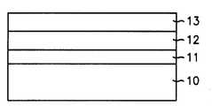
첨부된 도면 도 1은 종래기술에 따라 제조된 강유전체 캐패시터의 단면을 도시한 것으로, 그 유전체로서 SBT를 사용하고 있다.1 is a cross-sectional view of a ferroelectric capacitor manufactured according to the prior art, and SBT is used as the dielectric.
도시된 바와 같은 SBT 박막(11)을 사용한 강유전체 캐패시터 제조 공정시 일반적으로 보다 나은 강유전체 특성을 얻기 위해 800℃ 정도의 고온 증착 및 후속 고온 열처리를 통해 결정화된 SBT 박막(11)을 형성하게 된다.In the manufacturing process of the ferroelectric capacitor using the SBT thin film 11 as shown in general, in order to obtain better ferroelectric properties, the crystallized SBT thin film 11 is formed through high temperature deposition of about 800 ° C. and subsequent high temperature heat treatment.
이는 SBT 박막(11)은 다결정질(polycrystalline) 결정 구조하에서 높은 유전상수와 잔류분극 특성 등 강유전체로서의 성질을 제대로 나타낼 수 있기 때문이다. 그러나, 다결정질인 SBT 박막(11) 내의 결정립계가 누설전류의 전도 경로를 제공하기 때문에, 누설전류에 따른 유전손실을 가져오게 되어 강유전체 캐패시터 특성의 열화를 유발하는 문제점이 있었다.This is because the SBT thin film 11 can properly exhibit ferroelectric properties such as high dielectric constant and residual polarization characteristics under a polycrystalline crystal structure. However, since the grain boundary in the polycrystalline SBT thin film 11 provides a conduction path for leakage current, there is a problem of causing dielectric loss due to leakage current, causing deterioration of ferroelectric capacitor characteristics.
이러한 누설전류를 줄이기 위해서 다양한 전극의 사용, 불순물 첨가 등 여러 가지 방법이 시도되고 있으나, 아직까지 만족할 만한 결과를 나타내는 기술을 확보하지 못하고 있다. 또한, 결정화를 위한 고온의 열처리 공정시 SBT 박막 표면에서 비스무스(Bi) 원소의 휘발에 의한 박막 조성의 변화로 강유전체 특성을 제대로 나타내지 못하는 문제점이 있었다. 도면에서, 도면 부호 '10'은 기판, '12'는 하부전극, '13'은 상부전극을 각각 나타낸 것이다.In order to reduce the leakage current, various methods such as the use of various electrodes and the addition of impurities have been attempted, but have not yet secured a technology showing satisfactory results. In addition, there is a problem that the ferroelectric properties are not properly represented by the change of the thin film composition due to the volatilization of bismuth (Bi) element on the surface of the SBT thin film during the high temperature heat treatment process for crystallization. In the drawing, reference numeral '10' denotes a substrate, '12' denotes a lower electrode, and '13' denotes an upper electrode.
따라서, 다결정질의 장점을 살리면서도 누설전류를 줄이기 위해서는 현재와는 다른 방식의 강유전체 박막의 제조 공정이 필요하다.Therefore, in order to reduce the leakage current while utilizing the advantages of polycrystalline, a manufacturing process of a ferroelectric thin film different from the present method is required.
본 발명은 누설전류에 따른 유전손실을 감소시키는 강유전체 캐패시터 제조방법을 제공하는데 그 목적이 있다.An object of the present invention is to provide a method of manufacturing a ferroelectric capacitor that reduces the dielectric loss due to leakage current.
도 1은 종래기술에 따라 제조된 강유전체 캐패시터의 단면도.1 is a cross-sectional view of a ferroelectric capacitor prepared according to the prior art.
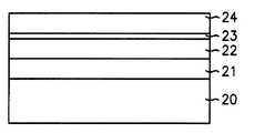
도 2는 본 발명의 일실시예에 따라 제조된 강유전체 캐패시터의 단면도.2 is a cross-sectional view of a ferroelectric capacitor manufactured according to an embodiment of the present invention.
도 3은 본 발명의 일실시예에 따른 강유전체 캐패시터 제조 공정 흐름도.3 is a flow chart of a ferroelectric capacitor manufacturing process according to an embodiment of the present invention.
* 도면의 주요 부분에 대한 부호의 설명* Explanation of symbols for the main parts of the drawings
20 : 기판 21 : 하부전극20: substrate 21: lower electrode
22 : 다결정질 SBT 박막 23 : 비정질 SBT 박막22: polycrystalline SBT thin film 23: amorphous SBT thin film
24 : 상부전극24: upper electrode
본 발명은 강유전체 캐패시터의 상부전극과 다결정질 SBT 박막 사이에 비스무스(Bi) 원소가 과량 함유된 비정질 SBT 박막을 얇은 두께로 형성하는 기술이다. 비정질 SBT 박막은 다결정질 SBT 박막에 비해 유전상수도 작고 강유전체로서의 특성을 나타내지 못하지만, 결정립계가 없기 때문에 박막 내부에 물질 전달 경로가 형성되지 않기 때문에 누설전류의 경로를 차단할 수 있다. 그리고, 이러한 효과를 얻기 위한 비정질 박막의 두께가 그다지 두꺼울 필요가 없으므로, 유전상수의 감소 등 강유전체 특성에 열화를 가져오는 영향은 미미할 것으로 여겨진다. 또한, 비정질 SBT 박막에 과량으로 첨가된 비스무스는 고온 증착 및 결정화 열처리 과정에서 손실된 비스무스 성분을 보충하는 효과를 가져온다.The present invention is a technique for forming an amorphous SBT thin film containing an excessive amount of bismuth (Bi) element between the upper electrode of the ferroelectric capacitor and the polycrystalline SBT thin film. Amorphous SBT thin films have a smaller dielectric constant and do not exhibit ferroelectric characteristics than polycrystalline SBT thin films, but because of the absence of grain boundaries, no material transfer path is formed in the thin film, thereby preventing the leakage current path. In addition, since the thickness of the amorphous thin film for obtaining such an effect does not need to be very thick, the effect of deteriorating ferroelectric properties such as a decrease in the dielectric constant is considered to be minimal. In addition, bismuth added in an excessive amount to the amorphous SBT thin film has the effect of supplementing the bismuth component lost during the high temperature deposition and crystallization heat treatment process.
상술한 본 발명의 기술적 원리로부터 제공되는 강유전체 캐패시터 제조방법은 소정의 하부 구조가 형성된 기판 상에 하부전극을 형성하는 제1 단계; 전체구조 상부에 다결정
이하, 첨부된 도면을 참조하여 본 발명의 실시예를 소개한다.Hereinafter, embodiments of the present invention will be described with reference to the accompanying drawings.
첨부된 도면 도 2는 본 발명의 일실시예에 따라 제조된 캐패시터의 단면을 도시한 것으로, 도면 부호 '20'은 기판, '21'은 하부전극, '22'는 다결정질 SBT 박막, '23'은 비정질 SBT 박막, '24'는 상부전극을 각각 나타낸 것이다.2 is a cross-sectional view of a capacitor manufactured in accordance with an embodiment of the present invention, '20' is a substrate, '21' is a lower electrode, '22' is a polycrystalline SBT thin film, '23' 'Is an amorphous SBT thin film,' 24 'is the upper electrode, respectively.
첨부된 도면 도 3은 도 2에 도시된 강유전체 캐패시터의 제조 공정 흐름도를 나타낸 것으로, 이하 도 2에 나타낸 도면 부호를 인용하여 본 발명의 일실시예에 따른 강유전체 캐패시터 제조 공정을 소개한다.FIG. 3 is a flowchart illustrating a manufacturing process of the ferroelectric capacitor illustrated in FIG. 2. Hereinafter, a process of manufacturing a ferroelectric capacitor according to an embodiment of the present invention will be introduced by referring to the reference numeral illustrated in FIG. 2.
우선, 소정의 하부 구조가 형성된 기판(20) 상에 하부전극(21)을 형성한다(100). 이때, 하부전극(21) 재료로서 Pt 또는 IrO, RuO 등의 금속산화물을 사용하며, 기판(20)과의 접착력을 향상시키고 불순물 상호 확산을 방지하기 위하여 Ti, TiN 등의 장벽 금속이 사용될 수도 있다.First, a
다음으로, 스퍼터링(sputtering) 등의 물리기상증착(PVD)법 또는 금속유기물 화학기상증착(MOCVD) 등의 화학기상증착(CVD)법을 사용하여 전체구조 상부에 SBT를 증착하고 결정화 열처리를 실시하여 50㎚∼300㎚ 두께의 다결정질 SBT 박막(22)을 형성한다(200). 이때, 다결정질 SBT 박막(22)은 비교적 휘발성이 강한 비스무스(Bi)의 성분비를 높여
이어서, 상온∼300℃의 저온에서 졸겔법, 금속유기물 화학기상증착법 등의 화학기상증착법을 사용하여 다결정질 SBT 박막(22) 상부에 30㎚∼50㎚ 두께의 비정질 SBT 박막(23)을 증착한다(300). 이때, 비정질 SBT 박막(23)의 증착시 다결정질 SBT 박막(22)의 손상을 방지하기 위하여 화학기상증착법을 사용하는 것이며, 300℃ 이하의 저온에서 증착하므로 박막의 결정화가 이루어지지 않는다. 여기서, 비정질 SBT 박막(23)은 후속 공정시 비스무스가 휘발되는 것을 고려하여 비스무스의 조성비를 높여
다음으로, 제2 SBT 박막(23) 상에 상부전극(24)을 형성한다(400). 이후, 캐패시터의 특성을 안정화시키기 위하여 열처리 공정 등을 실시한다. 이후, 사진 및 식각 공정을 진행하여 캐패시터를 디파인한다. 이때, 상부전극(24) 재료로서 하부전극(21)과 동일한 물질을 사용할 수 있으며, 필요한 경우 제2 SBT 박막(23)과 상부전극(24)간의 상호 작용(interaction)을 줄이기 위해 다른 물질들을 버퍼층(buffer layer)으로 사용할 수 있다. 또한, 식각후 열처리를 함으로써 식각시 손상을 입은 캐패시터의 특성을 개선할 수 있다.Next, the
이상에서 설명한 본 발명은 전술한 실시예 및 첨부된 도면에 의해 한정되는 것이 아니고, 본 발명의 기술적 사상을 벗어나지 않는 범위 내에서 여러 가지 치환, 변형 및 변경이 가능하다는 것이 본 발명이 속하는 기술분야에서 통상의 지식을 가진 자에게 있어 명백할 것이다.The present invention described above is not limited to the above-described embodiments and the accompanying drawings, and various substitutions, modifications, and changes can be made in the art without departing from the technical spirit of the present invention. It will be apparent to those of ordinary knowledge.
상술한 바와 같이 본 발명은 다결정질 SBT 박막과 상부전극 사이에 비정질 SBT층을 형성함으로써 누설전류에 따른 유전손실을 감소시키며, 이에 따라 소자의 신뢰도를 개선한다. 또한, 본 발명은 다결정질 SBT 박막의 증착 및 결정화 열처리시에 손실된 비스무스 성분을 보충함으로써, 강유전체 특성의 열화를 방지하며, 강유전체 본래의 특성을 유지하면서 신뢰도를 높임으로써 반도체 메모리 장치의 전기적 물성 향상 및 안정화에 기여한다.As described above, the present invention reduces the dielectric loss due to leakage current by forming an amorphous SBT layer between the polycrystalline SBT thin film and the upper electrode, thereby improving the reliability of the device. In addition, the present invention compensates for the deterioration of ferroelectric properties by supplementing the bismuth component lost during deposition and crystallization heat treatment of the polycrystalline SBT thin film, and improves electrical properties of the semiconductor memory device by increasing reliability while maintaining the original characteristics of the ferroelectric. And stabilization.
Claims (7)
Translated fromKoreanPriority Applications (4)
| Application Number | Priority Date | Filing Date | Title |
|---|---|---|---|
| KR1019970077897AKR100275121B1 (en) | 1997-12-30 | 1997-12-30 | Method for manufacturing ferroelectric capacitor |
| US09/224,654US6190924B1 (en) | 1997-12-30 | 1998-12-30 | Apparatus and method to form ferroelectric capacitors having low dielectric loss |
| CN98127109ACN1228559A (en) | 1997-12-30 | 1998-12-30 | Automatic telephone call transfer device and method in internet connection mode |
| TW088101217ATW439292B (en) | 1997-12-30 | 1999-01-27 | Method for forming a ferroelectric capacitor with low dielectric loss |
Applications Claiming Priority (1)
| Application Number | Priority Date | Filing Date | Title |
|---|---|---|---|
| KR1019970077897AKR100275121B1 (en) | 1997-12-30 | 1997-12-30 | Method for manufacturing ferroelectric capacitor |
Publications (2)
| Publication Number | Publication Date |
|---|---|
| KR19990057818A KR19990057818A (en) | 1999-07-15 |
| KR100275121B1true KR100275121B1 (en) | 2001-01-15 |
Family
ID=19529707
Family Applications (1)
| Application Number | Title | Priority Date | Filing Date |
|---|---|---|---|
| KR1019970077897AExpired - Fee RelatedKR100275121B1 (en) | 1997-12-30 | 1997-12-30 | Method for manufacturing ferroelectric capacitor |
Country Status (4)
| Country | Link |
|---|---|
| US (1) | US6190924B1 (en) |
| KR (1) | KR100275121B1 (en) |
| CN (1) | CN1228559A (en) |
| TW (1) | TW439292B (en) |
Cited By (1)
| Publication number | Priority date | Publication date | Assignee | Title |
|---|---|---|---|---|
| KR20030039893A (en)* | 2001-11-16 | 2003-05-22 | 주식회사 하이닉스반도체 | Capacitor in semiconductor device and the method for fabricating thereof |
Families Citing this family (18)
| Publication number | Priority date | Publication date | Assignee | Title |
|---|---|---|---|---|
| US20010013660A1 (en)* | 1999-01-04 | 2001-08-16 | Peter Richard Duncombe | Beol decoupling capacitor |
| AUPQ439299A0 (en)* | 1999-12-01 | 1999-12-23 | Silverbrook Research Pty Ltd | Interface system |
| KR20010045968A (en)* | 1999-11-09 | 2001-06-05 | 박종섭 | Method of manufacturing a capacitor in a semiconductor device |
| DE19963500C2 (en)* | 1999-12-28 | 2002-10-02 | Infineon Technologies Ag | Method for producing a structured layer containing metal oxide, in particular a ferroelectric or paraelectric layer |
| KR20010109610A (en)* | 2000-05-31 | 2001-12-12 | 박종섭 | A method for forming ferroelectric capacitor in semiconductor device |
| KR100390845B1 (en)* | 2001-06-30 | 2003-07-12 | 주식회사 하이닉스반도체 | Ferroelectric capacitor in semiconductor device and forming method thereof |
| JP3986859B2 (en)* | 2002-03-25 | 2007-10-03 | 富士通株式会社 | Thin film capacitor and manufacturing method thereof |
| KR20050010650A (en)* | 2003-07-22 | 2005-01-28 | 주식회사 하이닉스반도체 | Method of manufacturing ferroelectric capacitor |
| CN1317865C (en)* | 2003-10-30 | 2007-05-23 | 神达电脑股份有限公司 | communication switch |
| KR100585114B1 (en)* | 2003-12-05 | 2006-05-30 | 삼성전자주식회사 | Capacitor of semiconductor device having high dielectric film made of VTS or VAT material and manufacturing method thereof |
| FR2907592B1 (en)* | 2006-10-19 | 2008-12-26 | Commissariat Energie Atomique | THIN FILM CAPACITOR WITH HIGH STABILITY AND METHOD OF MANUFACTURE |
| JP4524698B2 (en)* | 2006-10-26 | 2010-08-18 | エルピーダメモリ株式会社 | Semiconductor device having capacitive element and method of manufacturing the same |
| FR2907593B1 (en)* | 2007-02-26 | 2009-01-23 | Commissariat Energie Atomique | METHOD FOR MANUFACTURING A CAPACITOR WITH HIGH STABILITY |
| FR2907594B1 (en)* | 2007-02-26 | 2008-12-26 | Commissariat Energie Atomique | METHOD FOR DETERMINING THE RESPECTIVE THICKNESS OF TWO SUPERIMPOSED THIN LAYERS |
| US7820506B2 (en) | 2008-10-15 | 2010-10-26 | Micron Technology, Inc. | Capacitors, dielectric structures, and methods of forming dielectric structures |
| JP5532505B2 (en)* | 2009-07-23 | 2014-06-25 | 日本電気硝子株式会社 | Glass film for condenser |
| JPWO2020045446A1 (en)* | 2018-08-31 | 2021-08-10 | Tdk株式会社 | Thin film capacitors and electronic circuit boards |
| US11665909B2 (en)* | 2020-07-23 | 2023-05-30 | Taiwan Semiconductor Manufacturing Co., Ltd. | FeRAM with laminated ferroelectric film and method forming same |
Citations (1)
| Publication number | Priority date | Publication date | Assignee | Title |
|---|---|---|---|---|
| JPH0936309A (en)* | 1995-07-14 | 1997-02-07 | Matsushita Electron Corp | Capacitive element manufacturing method |
Family Cites Families (9)
| Publication number | Priority date | Publication date | Assignee | Title |
|---|---|---|---|---|
| US5614018A (en) | 1991-12-13 | 1997-03-25 | Symetrix Corporation | Integrated circuit capacitors and process for making the same |
| EP0568064B1 (en) | 1992-05-01 | 1999-07-14 | Texas Instruments Incorporated | Pb/Bi-containing high-dielectric constant oxides using a non-Pb/Bi-containing perovskite as a buffer layer |
| US5566046A (en) | 1994-02-18 | 1996-10-15 | Texas Instruments Incorporated | Microelectronic device with capacitors having fine-grain dielectric material |
| US5426075A (en) | 1994-06-15 | 1995-06-20 | Ramtron International Corporation | Method of manufacturing ferroelectric bismuth layered oxides |
| JP3133922B2 (en) | 1995-06-09 | 2001-02-13 | シャープ株式会社 | Ferroelectric thin film coated substrate, method of manufacturing the same, and capacitor structure element |
| JP3135483B2 (en)* | 1995-06-22 | 2001-02-13 | 松下電子工業株式会社 | Semiconductor device and method of manufacturing the same |
| JP3137004B2 (en) | 1995-09-11 | 2001-02-19 | ソニー株式会社 | Method for manufacturing capacitor structure of semiconductor device |
| JP3891603B2 (en) | 1995-12-27 | 2007-03-14 | シャープ株式会社 | Ferroelectric thin film coated substrate, capacitor structure element, and method for manufacturing ferroelectric thin film coated substrate |
| JPH09260516A (en) | 1996-03-18 | 1997-10-03 | Sharp Corp | Ferroelectric thin film coated substrate and capacitor structure element using the same |
- 1997
- 1997-12-30KRKR1019970077897Apatent/KR100275121B1/ennot_activeExpired - Fee Related
- 1998
- 1998-12-30USUS09/224,654patent/US6190924B1/ennot_activeExpired - Lifetime
- 1998-12-30CNCN98127109Apatent/CN1228559A/enactivePending
- 1999
- 1999-01-27TWTW088101217Apatent/TW439292B/ennot_activeIP Right Cessation
Patent Citations (1)
| Publication number | Priority date | Publication date | Assignee | Title |
|---|---|---|---|---|
| JPH0936309A (en)* | 1995-07-14 | 1997-02-07 | Matsushita Electron Corp | Capacitive element manufacturing method |
Cited By (1)
| Publication number | Priority date | Publication date | Assignee | Title |
|---|---|---|---|---|
| KR20030039893A (en)* | 2001-11-16 | 2003-05-22 | 주식회사 하이닉스반도체 | Capacitor in semiconductor device and the method for fabricating thereof |
Also Published As
| Publication number | Publication date |
|---|---|
| CN1228559A (en) | 1999-09-15 |
| TW439292B (en) | 2001-06-07 |
| KR19990057818A (en) | 1999-07-15 |
| US6190924B1 (en) | 2001-02-20 |
Similar Documents
| Publication | Publication Date | Title |
|---|---|---|
| KR100275121B1 (en) | Method for manufacturing ferroelectric capacitor | |
| US5508226A (en) | Low temperature process for fabricating layered superlattice materialsand making electronic devices including same | |
| US6420740B1 (en) | Lead germanate ferroelectric structure with multi-layered electrode | |
| US6541281B2 (en) | Ferroelectric circuit element that can be fabricated at low temperatures and method for making the same | |
| US20020149040A1 (en) | Process for producing a strontium ruthenium oxide protective layer on a top electrode | |
| US6727156B2 (en) | Semiconductor device including ferroelectric capacitor and method of manufacturing the same | |
| US5955755A (en) | Semiconductor storage device and method for manufacturing the same | |
| US6713799B2 (en) | Electrodes for ferroelectric components | |
| US6495412B1 (en) | Semiconductor device having a ferroelectric capacitor and a fabrication process thereof | |
| US6080593A (en) | Method of manufacturing ferroelectric memory | |
| US6346424B1 (en) | Process for producing high-epsilon dielectric layer or ferroelectric layer | |
| KR100399074B1 (en) | Formation Method of FeRAM having BLT ferroelectric layer | |
| KR100265846B1 (en) | A method for fabricating ferroelectric capacitor in semiconductor device | |
| US6849468B2 (en) | Method for manufacturing ferroelectric random access memory capacitor | |
| JP4289843B2 (en) | Capacitor manufacturing method for semiconductor device | |
| KR100247474B1 (en) | Method for forming pzt ferroelectric capacitor | |
| KR100275120B1 (en) | Method for forming ferroelectric film of capacitors | |
| KR20010045968A (en) | Method of manufacturing a capacitor in a semiconductor device | |
| KR100321709B1 (en) | Method for forming capacitor of semiconductor memory device by using ain as glue layer | |
| KR20000042388A (en) | Ferroelectric capacitor of semiconductor device and fabrication method thereof | |
| KR100430686B1 (en) | Manufacturing method of storage electrode of semiconductor device | |
| KR100600290B1 (en) | Capacitor Formation Method of Semiconductor Device | |
| KR100772707B1 (en) | Capacitor of Ferroelectric Memory Device and Manufacturing Method Thereof | |
| KR20010064097A (en) | A method for forming high dielectrics capacitor in semiconductor device | |
| KR20000044603A (en) | Method for manufacturing platinum upper electrode of ferroelectric capacitor |
Legal Events
| Date | Code | Title | Description |
|---|---|---|---|
| A201 | Request for examination | ||
| PA0109 | Patent application | St.27 status event code:A-0-1-A10-A12-nap-PA0109 | |
| PA0201 | Request for examination | St.27 status event code:A-1-2-D10-D11-exm-PA0201 | |
| R17-X000 | Change to representative recorded | St.27 status event code:A-3-3-R10-R17-oth-X000 | |
| PG1501 | Laying open of application | St.27 status event code:A-1-1-Q10-Q12-nap-PG1501 | |
| E902 | Notification of reason for refusal | ||
| PE0902 | Notice of grounds for rejection | St.27 status event code:A-1-2-D10-D21-exm-PE0902 | |
| P11-X000 | Amendment of application requested | St.27 status event code:A-2-2-P10-P11-nap-X000 | |
| P13-X000 | Application amended | St.27 status event code:A-2-2-P10-P13-nap-X000 | |
| E701 | Decision to grant or registration of patent right | ||
| PE0701 | Decision of registration | St.27 status event code:A-1-2-D10-D22-exm-PE0701 | |
| R17-X000 | Change to representative recorded | St.27 status event code:A-3-3-R10-R17-oth-X000 | |
| GRNT | Written decision to grant | ||
| PR0701 | Registration of establishment | St.27 status event code:A-2-4-F10-F11-exm-PR0701 | |
| PR1002 | Payment of registration fee | St.27 status event code:A-2-2-U10-U11-oth-PR1002 Fee payment year number:1 | |
| PN2301 | Change of applicant | St.27 status event code:A-5-5-R10-R13-asn-PN2301 St.27 status event code:A-5-5-R10-R11-asn-PN2301 | |
| PG1601 | Publication of registration | St.27 status event code:A-4-4-Q10-Q13-nap-PG1601 | |
| PN2301 | Change of applicant | St.27 status event code:A-5-5-R10-R13-asn-PN2301 St.27 status event code:A-5-5-R10-R11-asn-PN2301 | |
| PR1001 | Payment of annual fee | St.27 status event code:A-4-4-U10-U11-oth-PR1001 Fee payment year number:4 | |
| PR1001 | Payment of annual fee | St.27 status event code:A-4-4-U10-U11-oth-PR1001 Fee payment year number:5 | |
| PR1001 | Payment of annual fee | St.27 status event code:A-4-4-U10-U11-oth-PR1001 Fee payment year number:6 | |
| PR1001 | Payment of annual fee | St.27 status event code:A-4-4-U10-U11-oth-PR1001 Fee payment year number:7 | |
| PR1001 | Payment of annual fee | St.27 status event code:A-4-4-U10-U11-oth-PR1001 Fee payment year number:8 | |
| PR1001 | Payment of annual fee | St.27 status event code:A-4-4-U10-U11-oth-PR1001 Fee payment year number:9 | |
| PR1001 | Payment of annual fee | St.27 status event code:A-4-4-U10-U11-oth-PR1001 Fee payment year number:10 | |
| PR1001 | Payment of annual fee | St.27 status event code:A-4-4-U10-U11-oth-PR1001 Fee payment year number:11 | |
| FPAY | Annual fee payment | Payment date:20110825 Year of fee payment:12 | |
| PR1001 | Payment of annual fee | St.27 status event code:A-4-4-U10-U11-oth-PR1001 Fee payment year number:12 | |
| PN2301 | Change of applicant | St.27 status event code:A-5-5-R10-R13-asn-PN2301 St.27 status event code:A-5-5-R10-R11-asn-PN2301 | |
| FPAY | Annual fee payment | Payment date:20120824 Year of fee payment:13 | |
| PR1001 | Payment of annual fee | St.27 status event code:A-4-4-U10-U11-oth-PR1001 Fee payment year number:13 | |
| PN2301 | Change of applicant | St.27 status event code:A-5-5-R10-R13-asn-PN2301 St.27 status event code:A-5-5-R10-R11-asn-PN2301 | |
| LAPS | Lapse due to unpaid annual fee | ||
| PC1903 | Unpaid annual fee | St.27 status event code:A-4-4-U10-U13-oth-PC1903 Not in force date:20130920 Payment event data comment text:Termination Category : DEFAULT_OF_REGISTRATION_FEE | |
| PC1903 | Unpaid annual fee | St.27 status event code:N-4-6-H10-H13-oth-PC1903 Ip right cessation event data comment text:Termination Category : DEFAULT_OF_REGISTRATION_FEE Not in force date:20130920 | |
| PN2301 | Change of applicant | St.27 status event code:A-5-5-R10-R13-asn-PN2301 St.27 status event code:A-5-5-R10-R11-asn-PN2301 | |
| P22-X000 | Classification modified | St.27 status event code:A-4-4-P10-P22-nap-X000 |