KR100274854B1 - Lead frame for semiconductor device and semiconductor device - Google Patents
Lead frame for semiconductor device and semiconductor deviceDownload PDFInfo
- Publication number
- KR100274854B1 KR100274854B1KR1019970060650AKR19970060650AKR100274854B1KR 100274854 B1KR100274854 B1KR 100274854B1KR 1019970060650 AKR1019970060650 AKR 1019970060650AKR 19970060650 AKR19970060650 AKR 19970060650AKR 100274854 B1KR100274854 B1KR 100274854B1
- Authority
- KR
- South Korea
- Prior art keywords
- semiconductor
- semiconductor element
- insulating tape
- semiconductor device
- lead frame
- Prior art date
- Legal status (The legal status is an assumption and is not a legal conclusion. Google has not performed a legal analysis and makes no representation as to the accuracy of the status listed.)
- Expired - Fee Related
Links
Images


Classifications
- H—ELECTRICITY
- H01—ELECTRIC ELEMENTS
- H01L—SEMICONDUCTOR DEVICES NOT COVERED BY CLASS H10
- H01L23/00—Details of semiconductor or other solid state devices
- H01L23/16—Fillings or auxiliary members in containers or encapsulations, e.g. centering rings
- H—ELECTRICITY
- H01—ELECTRIC ELEMENTS
- H01L—SEMICONDUCTOR DEVICES NOT COVERED BY CLASS H10
- H01L23/00—Details of semiconductor or other solid state devices
- H01L23/48—Arrangements for conducting electric current to or from the solid state body in operation, e.g. leads, terminal arrangements ; Selection of materials therefor
- H—ELECTRICITY
- H01—ELECTRIC ELEMENTS
- H01L—SEMICONDUCTOR DEVICES NOT COVERED BY CLASS H10
- H01L21/00—Processes or apparatus adapted for the manufacture or treatment of semiconductor or solid state devices or of parts thereof
- H01L21/02—Manufacture or treatment of semiconductor devices or of parts thereof
- H01L21/04—Manufacture or treatment of semiconductor devices or of parts thereof the devices having potential barriers, e.g. a PN junction, depletion layer or carrier concentration layer
- H01L21/50—Assembly of semiconductor devices using processes or apparatus not provided for in a single one of the groups H01L21/18 - H01L21/326 or H10D48/04 - H10D48/07 e.g. sealing of a cap to a base of a container
- H01L21/60—Attaching or detaching leads or other conductive members, to be used for carrying current to or from the device in operation
- H—ELECTRICITY
- H01—ELECTRIC ELEMENTS
- H01L—SEMICONDUCTOR DEVICES NOT COVERED BY CLASS H10
- H01L23/00—Details of semiconductor or other solid state devices
- H01L23/12—Mountings, e.g. non-detachable insulating substrates
- H—ELECTRICITY
- H01—ELECTRIC ELEMENTS
- H01L—SEMICONDUCTOR DEVICES NOT COVERED BY CLASS H10
- H01L23/00—Details of semiconductor or other solid state devices
- H01L23/28—Encapsulations, e.g. encapsulating layers, coatings, e.g. for protection
- H01L23/31—Encapsulations, e.g. encapsulating layers, coatings, e.g. for protection characterised by the arrangement or shape
- H01L23/3107—Encapsulations, e.g. encapsulating layers, coatings, e.g. for protection characterised by the arrangement or shape the device being completely enclosed
- H01L23/3121—Encapsulations, e.g. encapsulating layers, coatings, e.g. for protection characterised by the arrangement or shape the device being completely enclosed a substrate forming part of the encapsulation
- H01L23/3128—Encapsulations, e.g. encapsulating layers, coatings, e.g. for protection characterised by the arrangement or shape the device being completely enclosed a substrate forming part of the encapsulation the substrate having spherical bumps for external connection
- H—ELECTRICITY
- H01—ELECTRIC ELEMENTS
- H01L—SEMICONDUCTOR DEVICES NOT COVERED BY CLASS H10
- H01L23/00—Details of semiconductor or other solid state devices
- H01L23/48—Arrangements for conducting electric current to or from the solid state body in operation, e.g. leads, terminal arrangements ; Selection of materials therefor
- H01L23/488—Arrangements for conducting electric current to or from the solid state body in operation, e.g. leads, terminal arrangements ; Selection of materials therefor consisting of soldered or bonded constructions
- H01L23/495—Lead-frames or other flat leads
- H01L23/49572—Lead-frames or other flat leads consisting of thin flexible metallic tape with or without a film carrier
- H—ELECTRICITY
- H01—ELECTRIC ELEMENTS
- H01L—SEMICONDUCTOR DEVICES NOT COVERED BY CLASS H10
- H01L23/00—Details of semiconductor or other solid state devices
- H01L23/48—Arrangements for conducting electric current to or from the solid state body in operation, e.g. leads, terminal arrangements ; Selection of materials therefor
- H01L23/488—Arrangements for conducting electric current to or from the solid state body in operation, e.g. leads, terminal arrangements ; Selection of materials therefor consisting of soldered or bonded constructions
- H01L23/498—Leads, i.e. metallisations or lead-frames on insulating substrates, e.g. chip carriers
- H01L23/49811—Additional leads joined to the metallisation on the insulating substrate, e.g. pins, bumps, wires, flat leads
- H01L23/49816—Spherical bumps on the substrate for external connection, e.g. ball grid arrays [BGA]
- H—ELECTRICITY
- H01—ELECTRIC ELEMENTS
- H01L—SEMICONDUCTOR DEVICES NOT COVERED BY CLASS H10
- H01L23/00—Details of semiconductor or other solid state devices
- H01L23/562—Protection against mechanical damage
- H—ELECTRICITY
- H01—ELECTRIC ELEMENTS
- H01L—SEMICONDUCTOR DEVICES NOT COVERED BY CLASS H10
- H01L24/00—Arrangements for connecting or disconnecting semiconductor or solid-state bodies; Methods or apparatus related thereto
- H01L24/01—Means for bonding being attached to, or being formed on, the surface to be connected, e.g. chip-to-package, die-attach, "first-level" interconnects; Manufacturing methods related thereto
- H01L24/50—Tape automated bonding [TAB] connectors, i.e. film carriers; Manufacturing methods related thereto
- H—ELECTRICITY
- H01—ELECTRIC ELEMENTS
- H01L—SEMICONDUCTOR DEVICES NOT COVERED BY CLASS H10
- H01L2224/00—Indexing scheme for arrangements for connecting or disconnecting semiconductor or solid-state bodies and methods related thereto as covered by H01L24/00
- H01L2224/01—Means for bonding being attached to, or being formed on, the surface to be connected, e.g. chip-to-package, die-attach, "first-level" interconnects; Manufacturing methods related thereto
- H01L2224/02—Bonding areas; Manufacturing methods related thereto
- H01L2224/04—Structure, shape, material or disposition of the bonding areas prior to the connecting process
- H01L2224/05—Structure, shape, material or disposition of the bonding areas prior to the connecting process of an individual bonding area
- H01L2224/0554—External layer
- H01L2224/0555—Shape
- H01L2224/05552—Shape in top view
- H01L2224/05554—Shape in top view being square
- H—ELECTRICITY
- H01—ELECTRIC ELEMENTS
- H01L—SEMICONDUCTOR DEVICES NOT COVERED BY CLASS H10
- H01L2224/00—Indexing scheme for arrangements for connecting or disconnecting semiconductor or solid-state bodies and methods related thereto as covered by H01L24/00
- H01L2224/01—Means for bonding being attached to, or being formed on, the surface to be connected, e.g. chip-to-package, die-attach, "first-level" interconnects; Manufacturing methods related thereto
- H01L2224/42—Wire connectors; Manufacturing methods related thereto
- H01L2224/44—Structure, shape, material or disposition of the wire connectors prior to the connecting process
- H01L2224/45—Structure, shape, material or disposition of the wire connectors prior to the connecting process of an individual wire connector
- H01L2224/45001—Core members of the connector
- H01L2224/45099—Material
- H01L2224/451—Material with a principal constituent of the material being a metal or a metalloid, e.g. boron (B), silicon (Si), germanium (Ge), arsenic (As), antimony (Sb), tellurium (Te) and polonium (Po), and alloys thereof
- H—ELECTRICITY
- H01—ELECTRIC ELEMENTS
- H01L—SEMICONDUCTOR DEVICES NOT COVERED BY CLASS H10
- H01L2224/00—Indexing scheme for arrangements for connecting or disconnecting semiconductor or solid-state bodies and methods related thereto as covered by H01L24/00
- H01L2224/01—Means for bonding being attached to, or being formed on, the surface to be connected, e.g. chip-to-package, die-attach, "first-level" interconnects; Manufacturing methods related thereto
- H01L2224/42—Wire connectors; Manufacturing methods related thereto
- H01L2224/47—Structure, shape, material or disposition of the wire connectors after the connecting process
- H01L2224/48—Structure, shape, material or disposition of the wire connectors after the connecting process of an individual wire connector
- H01L2224/4805—Shape
- H01L2224/4809—Loop shape
- H01L2224/48091—Arched
- H—ELECTRICITY
- H01—ELECTRIC ELEMENTS
- H01L—SEMICONDUCTOR DEVICES NOT COVERED BY CLASS H10
- H01L2224/00—Indexing scheme for arrangements for connecting or disconnecting semiconductor or solid-state bodies and methods related thereto as covered by H01L24/00
- H01L2224/01—Means for bonding being attached to, or being formed on, the surface to be connected, e.g. chip-to-package, die-attach, "first-level" interconnects; Manufacturing methods related thereto
- H01L2224/42—Wire connectors; Manufacturing methods related thereto
- H01L2224/47—Structure, shape, material or disposition of the wire connectors after the connecting process
- H01L2224/48—Structure, shape, material or disposition of the wire connectors after the connecting process of an individual wire connector
- H01L2224/481—Disposition
- H01L2224/48151—Connecting between a semiconductor or solid-state body and an item not being a semiconductor or solid-state body, e.g. chip-to-substrate, chip-to-passive
- H01L2224/48221—Connecting between a semiconductor or solid-state body and an item not being a semiconductor or solid-state body, e.g. chip-to-substrate, chip-to-passive the body and the item being stacked
- H01L2224/48225—Connecting between a semiconductor or solid-state body and an item not being a semiconductor or solid-state body, e.g. chip-to-substrate, chip-to-passive the body and the item being stacked the item being non-metallic, e.g. insulating substrate with or without metallisation
- H01L2224/48227—Connecting between a semiconductor or solid-state body and an item not being a semiconductor or solid-state body, e.g. chip-to-substrate, chip-to-passive the body and the item being stacked the item being non-metallic, e.g. insulating substrate with or without metallisation connecting the wire to a bond pad of the item
- H—ELECTRICITY
- H01—ELECTRIC ELEMENTS
- H01L—SEMICONDUCTOR DEVICES NOT COVERED BY CLASS H10
- H01L2224/00—Indexing scheme for arrangements for connecting or disconnecting semiconductor or solid-state bodies and methods related thereto as covered by H01L24/00
- H01L2224/01—Means for bonding being attached to, or being formed on, the surface to be connected, e.g. chip-to-package, die-attach, "first-level" interconnects; Manufacturing methods related thereto
- H01L2224/42—Wire connectors; Manufacturing methods related thereto
- H01L2224/47—Structure, shape, material or disposition of the wire connectors after the connecting process
- H01L2224/48—Structure, shape, material or disposition of the wire connectors after the connecting process of an individual wire connector
- H01L2224/484—Connecting portions
- H01L2224/48463—Connecting portions the connecting portion on the bonding area of the semiconductor or solid-state body being a ball bond
- H01L2224/48465—Connecting portions the connecting portion on the bonding area of the semiconductor or solid-state body being a ball bond the other connecting portion not on the bonding area being a wedge bond, i.e. ball-to-wedge, regular stitch
- H—ELECTRICITY
- H01—ELECTRIC ELEMENTS
- H01L—SEMICONDUCTOR DEVICES NOT COVERED BY CLASS H10
- H01L24/00—Arrangements for connecting or disconnecting semiconductor or solid-state bodies; Methods or apparatus related thereto
- H01L24/01—Means for bonding being attached to, or being formed on, the surface to be connected, e.g. chip-to-package, die-attach, "first-level" interconnects; Manufacturing methods related thereto
- H01L24/42—Wire connectors; Manufacturing methods related thereto
- H01L24/44—Structure, shape, material or disposition of the wire connectors prior to the connecting process
- H01L24/45—Structure, shape, material or disposition of the wire connectors prior to the connecting process of an individual wire connector
- H—ELECTRICITY
- H01—ELECTRIC ELEMENTS
- H01L—SEMICONDUCTOR DEVICES NOT COVERED BY CLASS H10
- H01L24/00—Arrangements for connecting or disconnecting semiconductor or solid-state bodies; Methods or apparatus related thereto
- H01L24/01—Means for bonding being attached to, or being formed on, the surface to be connected, e.g. chip-to-package, die-attach, "first-level" interconnects; Manufacturing methods related thereto
- H01L24/42—Wire connectors; Manufacturing methods related thereto
- H01L24/47—Structure, shape, material or disposition of the wire connectors after the connecting process
- H01L24/48—Structure, shape, material or disposition of the wire connectors after the connecting process of an individual wire connector
- H—ELECTRICITY
- H01—ELECTRIC ELEMENTS
- H01L—SEMICONDUCTOR DEVICES NOT COVERED BY CLASS H10
- H01L24/00—Arrangements for connecting or disconnecting semiconductor or solid-state bodies; Methods or apparatus related thereto
- H01L24/80—Methods for connecting semiconductor or other solid state bodies using means for bonding being attached to, or being formed on, the surface to be connected
- H01L24/86—Methods for connecting semiconductor or other solid state bodies using means for bonding being attached to, or being formed on, the surface to be connected using tape automated bonding [TAB]
- H—ELECTRICITY
- H01—ELECTRIC ELEMENTS
- H01L—SEMICONDUCTOR DEVICES NOT COVERED BY CLASS H10
- H01L2924/00—Indexing scheme for arrangements or methods for connecting or disconnecting semiconductor or solid-state bodies as covered by H01L24/00
- H01L2924/0001—Technical content checked by a classifier
- H01L2924/00014—Technical content checked by a classifier the subject-matter covered by the group, the symbol of which is combined with the symbol of this group, being disclosed without further technical details
- H—ELECTRICITY
- H01—ELECTRIC ELEMENTS
- H01L—SEMICONDUCTOR DEVICES NOT COVERED BY CLASS H10
- H01L2924/00—Indexing scheme for arrangements or methods for connecting or disconnecting semiconductor or solid-state bodies as covered by H01L24/00
- H01L2924/01—Chemical elements
- H01L2924/01023—Vanadium [V]
- H—ELECTRICITY
- H01—ELECTRIC ELEMENTS
- H01L—SEMICONDUCTOR DEVICES NOT COVERED BY CLASS H10
- H01L2924/00—Indexing scheme for arrangements or methods for connecting or disconnecting semiconductor or solid-state bodies as covered by H01L24/00
- H01L2924/01—Chemical elements
- H01L2924/01029—Copper [Cu]
- H—ELECTRICITY
- H01—ELECTRIC ELEMENTS
- H01L—SEMICONDUCTOR DEVICES NOT COVERED BY CLASS H10
- H01L2924/00—Indexing scheme for arrangements or methods for connecting or disconnecting semiconductor or solid-state bodies as covered by H01L24/00
- H01L2924/01—Chemical elements
- H01L2924/01033—Arsenic [As]
- H—ELECTRICITY
- H01—ELECTRIC ELEMENTS
- H01L—SEMICONDUCTOR DEVICES NOT COVERED BY CLASS H10
- H01L2924/00—Indexing scheme for arrangements or methods for connecting or disconnecting semiconductor or solid-state bodies as covered by H01L24/00
- H01L2924/01—Chemical elements
- H01L2924/01057—Lanthanum [La]
- H—ELECTRICITY
- H01—ELECTRIC ELEMENTS
- H01L—SEMICONDUCTOR DEVICES NOT COVERED BY CLASS H10
- H01L2924/00—Indexing scheme for arrangements or methods for connecting or disconnecting semiconductor or solid-state bodies as covered by H01L24/00
- H01L2924/01—Chemical elements
- H01L2924/01082—Lead [Pb]
- H—ELECTRICITY
- H01—ELECTRIC ELEMENTS
- H01L—SEMICONDUCTOR DEVICES NOT COVERED BY CLASS H10
- H01L2924/00—Indexing scheme for arrangements or methods for connecting or disconnecting semiconductor or solid-state bodies as covered by H01L24/00
- H01L2924/15—Details of package parts other than the semiconductor or other solid state devices to be connected
- H01L2924/151—Die mounting substrate
- H01L2924/153—Connection portion
- H01L2924/1531—Connection portion the connection portion being formed only on the surface of the substrate opposite to the die mounting surface
- H01L2924/15311—Connection portion the connection portion being formed only on the surface of the substrate opposite to the die mounting surface being a ball array, e.g. BGA
- H—ELECTRICITY
- H01—ELECTRIC ELEMENTS
- H01L—SEMICONDUCTOR DEVICES NOT COVERED BY CLASS H10
- H01L2924/00—Indexing scheme for arrangements or methods for connecting or disconnecting semiconductor or solid-state bodies as covered by H01L24/00
- H01L2924/15—Details of package parts other than the semiconductor or other solid state devices to be connected
- H01L2924/151—Die mounting substrate
- H01L2924/153—Connection portion
- H01L2924/1532—Connection portion the connection portion being formed on the die mounting surface of the substrate
- H—ELECTRICITY
- H01—ELECTRIC ELEMENTS
- H01L—SEMICONDUCTOR DEVICES NOT COVERED BY CLASS H10
- H01L2924/00—Indexing scheme for arrangements or methods for connecting or disconnecting semiconductor or solid-state bodies as covered by H01L24/00
- H01L2924/15—Details of package parts other than the semiconductor or other solid state devices to be connected
- H01L2924/151—Die mounting substrate
- H01L2924/156—Material
- H01L2924/15786—Material with a principal constituent of the material being a non metallic, non metalloid inorganic material
- H01L2924/15787—Ceramics, e.g. crystalline carbides, nitrides or oxides
- H—ELECTRICITY
- H01—ELECTRIC ELEMENTS
- H01L—SEMICONDUCTOR DEVICES NOT COVERED BY CLASS H10
- H01L2924/00—Indexing scheme for arrangements or methods for connecting or disconnecting semiconductor or solid-state bodies as covered by H01L24/00
- H01L2924/15—Details of package parts other than the semiconductor or other solid state devices to be connected
- H01L2924/181—Encapsulation
- H01L2924/1815—Shape
- H—ELECTRICITY
- H05—ELECTRIC TECHNIQUES NOT OTHERWISE PROVIDED FOR
- H05K—PRINTED CIRCUITS; CASINGS OR CONSTRUCTIONAL DETAILS OF ELECTRIC APPARATUS; MANUFACTURE OF ASSEMBLAGES OF ELECTRICAL COMPONENTS
- H05K3/00—Apparatus or processes for manufacturing printed circuits
- H05K3/30—Assembling printed circuits with electric components, e.g. with resistor
- H05K3/32—Assembling printed circuits with electric components, e.g. with resistor electrically connecting electric components or wires to printed circuits
- H05K3/34—Assembling printed circuits with electric components, e.g. with resistor electrically connecting electric components or wires to printed circuits by soldering
- H05K3/341—Surface mounted components
- H05K3/3421—Leaded components
- H05K3/3426—Leaded components characterised by the leads
- H—ELECTRICITY
- H05—ELECTRIC TECHNIQUES NOT OTHERWISE PROVIDED FOR
- H05K—PRINTED CIRCUITS; CASINGS OR CONSTRUCTIONAL DETAILS OF ELECTRIC APPARATUS; MANUFACTURE OF ASSEMBLAGES OF ELECTRICAL COMPONENTS
- H05K3/00—Apparatus or processes for manufacturing printed circuits
- H05K3/30—Assembling printed circuits with electric components, e.g. with resistor
- H05K3/32—Assembling printed circuits with electric components, e.g. with resistor electrically connecting electric components or wires to printed circuits
- H05K3/34—Assembling printed circuits with electric components, e.g. with resistor electrically connecting electric components or wires to printed circuits by soldering
- H05K3/341—Surface mounted components
- H05K3/3431—Leadless components
- H05K3/3436—Leadless components having an array of bottom contacts, e.g. pad grid array or ball grid array components
Landscapes
- Engineering & Computer Science (AREA)
- Microelectronics & Electronic Packaging (AREA)
- Computer Hardware Design (AREA)
- Power Engineering (AREA)
- Physics & Mathematics (AREA)
- Condensed Matter Physics & Semiconductors (AREA)
- General Physics & Mathematics (AREA)
- Manufacturing & Machinery (AREA)
- Wire Bonding (AREA)
- Lead Frames For Integrated Circuits (AREA)
Abstract
Translated fromKoreanDescription
Translated fromKorean본 발명은 표면에 다수의 배선패턴 및 다수의 전극패드를 마련한 테이프형상의 절연부재를 금속판형상에 접착하고, 그 금속판에 반도체소자를 장전하고, 배선패턴과 반도체소자의 전극을 전기적으로 접속하고, 또 땜납범프를 외부단자로 해서 전극패드에 접속한 반도체장치의 구조에 관한 것으로서, 특히 외부단자의 접속신뢰성과 제조상의 생산성이 우수한 반도체장치에 관한 것이다.According to the present invention, a tape-shaped insulating member provided with a plurality of wiring patterns and a plurality of electrode pads is adhered to a metal plate, a semiconductor element is loaded on the metal plate, and the wiring pattern and the electrodes of the semiconductor element are electrically connected. The present invention also relates to a structure of a semiconductor device in which a solder bump is connected to an electrode pad with an external terminal, and more particularly, to a semiconductor device having excellent connection reliability and productivity in manufacturing an external terminal.
최근, 반도체장치의 고집적화나 다핀화가 진전되는 가운데 반도체패키지의 외부단자를 종래의 리이드를 사용한 1차원배열에서 금속범프를 사용한 2차원배열로 변화하고, 핀수(단자수)를 대폭으로 증가시키는 기술이 실용화되고 있다. 구체적인 구조의 하나는 프린트기판에 반도체소자를 탑재하고, 그 프린트기판의 이면에 금속범프를 배치한 구조가 미국특허 5, 216, 278호에 개시되어 있다. 이 구조는 일반적으로 BGA(볼그리드어레이)라 불리우고 있다.In recent years, as semiconductor devices have been highly integrated and multi-pinned, a technology for changing the external terminal of a semiconductor package from a one-dimensional array using a conventional lead to a two-dimensional array using metal bumps and significantly increasing the number of pins (terminal number) has been developed. It is put to practical use. One of the specific structures is disclosed in US Pat. No. 5,216,278, in which a semiconductor device is mounted on a printed board and metal bumps are disposed on the back surface of the printed board. This structure is commonly called BGA (ball grid array).
한편, 반도체패키지를 반도체소자의 치수까지 극력 작게 한 구조의 반도체장치가 개발되고 있으며, 이와 같은 반도체장치는 일반적으로 CSP(칩사이즈패키지 또는 칩스케일패키지)라 불리우고 있다. CSP의 종래기술로서는 일본국 특허공개 평성6-504408호에 개시되어 있는 바와 같이, 반도체소자의 회로형성면에 유연재를 거쳐서 배선패턴과 외부단자를 마련한 절연테이프를 탑재하고, 배선패턴과 반도체소자의 전극을 전기적으로 접속한 구조의 반도체장치가 있다. 또, 일본국 특허공개 공보 평성6-224259호에는 스루홀을 마련한 세라믹기판에 반도체소자를 탑재하고, 그 세라믹기판의 반대면에 전극을 마련하고, 그것을 프린트기판에 실장하는 구조가 개시되어 있다. 또, 일본국 특허공개공보 평성6-302604호에는 반도체소자의 회로형성면에 금속배선패턴을 형성하고, 이 금속배선패턴에 외부단자를 마련한 구조의 CSP가 개시되어 있다.On the other hand, a semiconductor device having a structure in which the semiconductor package is made as small as possible to the dimensions of the semiconductor device has been developed. Such a semiconductor device is generally called a CSP (chip size package or chip scale package). As a conventional technique of CSP, as disclosed in Japanese Patent Application Laid-Open No. Hei 6-504408, an insulating tape provided with a wiring pattern and external terminals through a flexible material is mounted on a circuit forming surface of a semiconductor device, and the wiring pattern and the semiconductor device are provided. There is a semiconductor device having a structure in which the electrodes of the electrode are electrically connected. In addition, Japanese Patent Application Laid-Open No. Hei 6-224259 discloses a structure in which a semiconductor element is mounted on a ceramic substrate provided with a through hole, an electrode is provided on the opposite side of the ceramic substrate, and the semiconductor substrate is mounted on a printed circuit board. Also, Japanese Patent Laid-Open Publication No. Hei 6-302604 discloses a CSP having a structure in which a metal wiring pattern is formed on a circuit formation surface of a semiconductor element and an external terminal is provided on the metal wiring pattern.
또, 일본국 특허공개공보 평성 8-88293호에는 반도체소자의 주위에 배선패턴과 땜납범프(외부단자)를 마련한 절연테이프를 마련하고, 배선패턴과 반도체소자의 전극을 전기적으로 접속한 구조의 반도체장치가 개시되어 있다.In addition, Japanese Patent Application Laid-Open No. 8-88293 provides an insulating tape having wiring patterns and solder bumps (external terminals) provided around the semiconductor elements, and a semiconductor having a structure in which the wiring patterns and the electrodes of the semiconductor elements are electrically connected. An apparatus is disclosed.
상술한 종래기술 중, 일본국 특허공개공보 평성8-88293호에 기재된 반도체장치, 즉 반도체소자의 주위에 절연테이프를 마련한 구조의 반도체장치는 패키지의 소형화와 다핀화를 동시에 달성할 수 있는 구조이다. 이 구조에서는 배선으로 절연테이프를 사용하고 있으므로, 프린트기판에 비해 배선패턴을 가늘게 할 수 있고, 그 결과 외부단자로서의 땜납범프의 피치도 작게 할 수 있어 패키지외주를 작게 하는 것이 가능하다. 또, 반도체소자의 외측에 땜납범프를 마련하고 있으므로, 반도체소자의 크기에 관계없이 다수의 범프를 마련할 수 있다.Among the above-mentioned prior arts, the semiconductor device described in Japanese Patent Application Laid-open No. Hei 8-88293, that is, a semiconductor device having an insulating tape provided around the semiconductor device, is capable of simultaneously achieving a compact package and multiple pinning. . In this structure, since the insulating tape is used as the wiring, the wiring pattern can be made thinner than the printed circuit board. As a result, the pitch of the solder bumps as the external terminals can be made smaller, and the package outer periphery can be made smaller. Further, since solder bumps are provided on the outside of the semiconductor element, a large number of bumps can be provided regardless of the size of the semiconductor element.
그러나, 상기 종래기술의 구조를 갖는 반도체장치에서는 다음에 설명하는 바와 같은 개선할 점이 있었다.However, the semiconductor device having the structure of the prior art has the following improvements.
제1의 점은 생산성에 관한 것이다. 이 구조에서는 강성이 낮은 절연테이프를 사용하므로 상기 종래기술에서 설명되어 있는 바와 같이 절연테이프를 보강하기 위해 그의 테이프의 이면측에 금속판을 접착할 필요가 있다. 이와 같이 금속판을 접착하지 않으면 테이프의 평탄도를 유지할 수 없으므로, 땜납범프의 선단에 단차가 생겨 접속신뢰성이 현저히 저하하게 된다. 그런데, 접속신뢰성을 확보하기 위해 반도체소자에 대응해서 개별적으로 금속판을 제작하여 절연테이프에 접착하는 것은 생산성을 현저히 저해한다.The first point relates to productivity. In this structure, since an insulating tape having a low rigidity is used, it is necessary to adhere a metal plate to the back side of its tape to reinforce the insulating tape as described in the prior art. Thus, since the flatness of a tape cannot be maintained unless a metal plate is adhere | attached, a step will arise in the front-end | tip of a solder bump, and connection reliability will fall remarkably. By the way, in order to secure connection reliability, separately manufacturing metal plates corresponding to semiconductor elements and adhering them to insulating tapes significantly hinders productivity.
제2의 점은 절연테이프의 평탄도에 관한 것이다. 상기와 같이 개별적으로 금속판을 제작해서 절연테이프에 접착하는 경우, 접착제의 두께를 균일하게 유지할 수 없게 되거나 또는 절연테이프의 감기려고 하는 성질(감기성질) 등에 의한 휘어짐을 해소할 수 없는 경우가 있다. 절연테이프의 평탄도가 나쁘면, 외부단자인 땜납범프의 높이에 편차가 생겨 접속신뢰성이 저하한다.The second point concerns the flatness of the insulating tape. In the case where the metal plates are separately manufactured and bonded to the insulating tape as described above, the thickness of the adhesive may not be maintained uniformly, or the bending due to the nature (cold property) of the insulating tape may not be eliminated. If the flatness of the insulating tape is poor, the height of the solder bumps, which are external terminals, is varied, and connection reliability is lowered.
본 발명의 목적은 상기와 같은 점을 극복하여 외부단자의 접속신뢰성과 제조상의 생상성을 향상시키는 것이 가능한 반도체장치를 제공하는 것이다.SUMMARY OF THE INVENTION An object of the present invention is to provide a semiconductor device capable of improving the connection reliability and manufacturing productivity of an external terminal by overcoming the above points.
제1도는 본 발명의 제1 실시예에 의한 반도체장치의 사시도.1 is a perspective view of a semiconductor device according to a first embodiment of the present invention.
제2도는 제1도에 도시한 반도체장치의 중앙부분의 단면도.2 is a cross-sectional view of a central portion of the semiconductor device shown in FIG.
제3도는 제1도 및 제2도에 도시한 반도체장치의 제조공정을 도시한 도면.FIG. 3 is a diagram showing a manufacturing process of the semiconductor device shown in FIGS.
제4도는 제1도 및 제2도에 도시한 반도체장치의 제조공정을 도시한 도면으로서, 제3도에 계속되는 공정을 도시한 도면.FIG. 4 is a diagram showing the manufacturing process of the semiconductor device shown in FIGS. 1 and 2, and showing the process following FIG.
제5도는 제1도의 V방향에서 본 도면으로서, 반도체장치의 절단끝면을 도시한 도면.5 is a view seen from the direction V in FIG. 1, showing a cut end face of the semiconductor device.
제6도는 본 발명의 제2 실시예에 의한 반도체장치의 사시도로서, 봉지수지에 의해 반도체소자의 회로형성면 및 측면을 봉지하기 전의 상태를 도시한 도면.FIG. 6 is a perspective view of a semiconductor device according to a second embodiment of the present invention, showing a state before encapsulating the circuit forming surface and the side surface of the semiconductor element with a sealing resin;
제7도는 본 발명의 제3 실시예에 의한 반도체장치의 사시도로서, 봉지수지에 의해 반도체소자의 회로형성면 및 측면을 봉지하기 전의 상태를 도시한 도면.FIG. 7 is a perspective view of a semiconductor device according to a third embodiment of the present invention, showing a state before encapsulating the circuit forming surface and the side surface of the semiconductor element with a sealing resin.
제8도는 본 발명의 제4 실시예에 의한 반도체장치의 사시도.8 is a perspective view of a semiconductor device according to a fourth embodiment of the present invention.
제9도는 제8도에 도시한 반도체장치의 중앙부분의 단면도.FIG. 9 is a sectional view of a central portion of the semiconductor device shown in FIG.
제10도는 제8도 및 제9도에 도시한 반도체장치의 제조공정을 도시한 도면.FIG. 10 is a diagram showing the manufacturing process of the semiconductor device shown in FIGS. 8 and 9;
제11도는 본 발명의 제5 실시예에 의한 반도체장치의 사시도.11 is a perspective view of a semiconductor device according to a fifth embodiment of the present invention.
제12도는 제11도의 반도체장치를 프린트기판에 실장했을 때의 중앙부분의 단면도.FIG. 12 is a sectional view of a central portion when the semiconductor device of FIG. 11 is mounted on a printed board.
제13도는 제6 실시예에 의한 반도체장치를 도시한 도면으로서, 그 반도체장치를 프린트기판에 실장했을 때의 중앙부분의 단면도.FIG. 13 is a diagram showing the semiconductor device according to the sixth embodiment, which is a sectional view of a central portion when the semiconductor device is mounted on a printed board.
* 도면의 주요부분에 대한 부호의 설명* Explanation of symbols for main parts of the drawings
1 : 반도체소자 1a : (반도체장치(1)의) 측벽DESCRIPTION OF SYMBOLS 1:
2 : (반도체장치(1)의) 전극 3 : 절연테이프2: electrode (of semiconductor device 1) 3: insulating tape
3a, 3b, 3c : (절연테이프의) 구멍3a, 3b, 3c: holes (of insulating tape)
3A : 절연테이프 4 : 배선패턴3A: insulating tape 4: wiring pattern
5 : 패드 6 : 금속판5: pad 6: metal plate
7 : 봉지수지 8 : 땜납범프7: encapsulation resin 8: solder bump
9, 9A, 9c : 리이드프레임 9a, 9b : (리이드프레임의) 구멍9, 9A, 9c:
10 : 땜납볼 11 : 와이어10 solder ball 11: wire
12 : 소자탑재부 12a : 절연테이프탑재부12:
12b : 연결용 단차부 13 : 슬릿12b: connection step portion 13: slit
14 : 돌기리이드 15 : 프린트기판14: protrusion guide 15: printed board
15a : (프린트기판의) 전극 15b : 돌기리이드접합부15a: electrode (of the printed circuit board) 15b: protrusion lead joint
16 : 땜납 20 : 접착제16: solder 20: adhesive
30 : 가공홈30: processing groove
상기 목적을 달성하기 위해, 본 발명에 의하면 반도체소자, 표면에 다수의 배선패턴과 다수의 전극패드를 마련한 절연테이프 및 그 절연테이프의 배선패턴을 마련한 면과는 반대측의 면에 접착제를 거쳐서 접착한 금속판을 갖고, 상기 배선패턴과 반도체소자의 전극을 전기적으로 접속하고 또한 상기 전극패드에 다수의 땜납범프를 접속하고 적어도 상기 반도체소자의 회로형성면을 봉지수지에 의해 피복한 반도체장치에 있어서, 상기 패키지의 적어도 하나의 측벽이 절단끝면으로 구성되고, 그의 측벽에 있어서의 상기 절연테이프, 접착제 및 금속판의 절단끝면이 일치하고 있는 것을 특징으로 하는 반도체장치가 제공된다.In order to achieve the above object, according to the present invention, a semiconductor device, an insulating tape provided with a plurality of wiring patterns and a plurality of electrode pads on the surface, and a surface opposite to the surface provided with a wiring pattern of the insulating tape are bonded to each other with an adhesive. A semiconductor device having a metal plate, electrically connecting the wiring pattern and an electrode of a semiconductor element, connecting a plurality of solder bumps to the electrode pad, and covering at least a circuit forming surface of the semiconductor element with a sealing resin. At least one side wall of the package is composed of a cut end face, and the cut end face of the insulating tape, the adhesive, and the metal plate on the side wall thereof is provided so as to provide a semiconductor device.
상기와 같이 구성된 본 발명의 반도체장치에 있어서는 패키지의 적어도 하나의 측벽을 절단끝면으로 하고, 그 측벽에 있어서의 절연테이프, 접착제 및 금속판의 절단끝면이 일치하는 구성으로 한다. 이와 같은 구성은 금속판의 기본으로 되는 리이드프레임에 절연테이프를 접착하고, 또 리이드프레임에 다수의 반도체소자를 장전하고, 절연테이프에 마련된 배선패턴과 반도체소자의 전극의 전기적 접속을 실행하고, 각 반도체소자의 회로형성면에 봉지수지에 의한 봉지를 실행한후에 리이드프레임을 절단하고 반도체소자의 각각에 대응하는 금속판을 동시에 형성하는 것에 의해 형성된다. 즉, 최종적으로 리이드프레임의 절단에 의해서 개개의 반도체장치로 분할했을 때에 어느 하나의 측벽이 절단끝면으로 되고, 그 측벽에 있어서의 절연테이프, 접착제 및 금속판의 절단끝면이 일치하고 따라서 절단에 수반되어 생기는 단면의 홈(손상)이 연속된 상태로 된다.In the semiconductor device of the present invention configured as described above, at least one sidewall of the package is used as the cut end surface, and the cut end surfaces of the insulating tape, the adhesive, and the metal plate on the side wall are coincident with each other. In such a structure, an insulating tape is adhered to a lead frame, which is the basis of a metal plate, and a plurality of semiconductor elements are loaded on the lead frame, and electrical connection between wiring patterns provided on the insulating tape and electrodes of the semiconductor elements is performed. After encapsulation with the encapsulating resin on the circuit forming surface of the element, the lead frame is cut and formed by simultaneously forming metal plates corresponding to each of the semiconductor elements. That is, when finally divided into individual semiconductor devices by cutting the lead frame, any one side wall becomes the cutting end surface, and the cutting end surfaces of the insulating tape, the adhesive and the metal plate in the side wall coincide with each other and are thus accompanied by the cutting. Grooves (damages) of cross sections are formed in a continuous state.
이와 같이 개개의 반도체패키지의 구성을 리이드프레임에 형성하고 나서 분할하므로여러개의 반도체패키지를 동시에 제조할 수 있어 생산성이 현저히 향상한다. 또, 최초에 단순한 형상의 2종류의 판형상부재 즉 리이드프레임과 절연테이프를 접착할 뿐이므로, 경우에 따라서 예를 들면 프레스나 로울러 등 다양한 방식으로 용이하게 접착을 실행할 수 있고, 접착제의 두께를 균일하게 할 수 있으며 또한 테이프에 감기성질이 있는 경우에도 그 감기성질을 제거하는 것도 용이하다. 따라서, 절연테이프의 평탄도를 향상시키는 것이 가능하게 되어 외부단자로서의 땜납범프의 접속신뢰성을 향상시킬 수 있다.Thus, since the structure of each semiconductor package is formed in a lead frame and divided, it is possible to manufacture several semiconductor packages at the same time, and the productivity is remarkably improved. In addition, since only two types of plate-shaped members having a simple shape, that is, a lead frame and an insulating tape are first adhered to each other, the adhesive can be easily carried out in various ways, for example, a press or a roller. It can be made uniform and it is also easy to remove the winding properties even if the tape has winding properties. Therefore, the flatness of the insulating tape can be improved, and the connection reliability of the solder bumps as the external terminals can be improved.
또, 종래에서는 봉지수지로서 생산성이 낮아 봉지후의 형상의 불균일이 많은 포팅수지를 사용하는 경우가 많고, 이 경우에는 봉지의 신뢰성이 불충분한 경우가 있었지만, 본 발명에서는 수지에 의한 봉지시에는 반도체패키지가 개개로 분할되어 있지 않은 상태이므로 통상의 리이드를 갖는 패키지를 위해 사용되고 있는 트랜스퍼몰드법을 사용할 수 있다. 이것에 의해서도 생상성이 향상됨과 동시에 봉지의 신뢰성도 향상한다.In the past, potting resins having low productivity due to low productivity due to low productivity are often used as sealing resins. In this case, the reliability of the sealing bags may be insufficient. However, in the present invention, semiconductor packages are used during sealing with resins. Since is not divided into pieces, the transfer mold method used for a package having a normal lead can be used. This also improves the productivity and the reliability of the encapsulation.
상기와 같은 반도체장치의 금속판은 바람직학는 반도체소자를 탑재하는 소자탑재부 및 소자탑재부의 주위에 위치하고 절연테이프를 탑재하는 절연테이프 탑재부를 갖고, 상기 소자탑재부 상면은 상기 절연테이프 탑재부 표면보다 낮은 위치에 있고, 또한 그 소자탑재부 및 절연테이프탑재부는 절연테이프탑재부와 소자탑재부의 경계보다 외측에서 시작되어 소자탑재부의 외주에 이르는 연결용단차부에 의해서 연결된다.The metal plate of the semiconductor device as described above preferably has an element mounting portion for mounting a semiconductor element and an insulation tape mounting portion located around the element mounting portion and for mounting an insulating tape, and the upper surface of the element mounting portion is at a lower position than the surface of the insulating tape mounting portion. In addition, the element mounting portion and the insulating tape mounting portion are connected by a connection step portion that starts outside the boundary between the insulating tape mounting portion and the element mounting portion and reaches the outer periphery of the element mounting portion.
이와 같이 소자탑재부 상면이 절연테이프탑재부 표면보다 낮은 위치에 있으므로, 반도체소자가 절연테이프상면에서 돌출하는 것을 방지하는 것이 가능하게 된다. 후술하는 바와 같이, 와이어본딩을 실행할 때에는 반도체소자가 고정되어 있을 필요가 있지만, 이 경우에는 금속판의 일부인 소자탑재부에 반도체소자가 탑재되고 고정되므로 와이어본딩을 안정하게 확실히 실행하는 것이 가능하게 된다.Thus, since the upper surface of the element mounting portion is located at a lower position than the surface of the insulating tape mounting portion, it is possible to prevent the semiconductor element from protruding from the upper surface of the insulating tape. As will be described later, the semiconductor element needs to be fixed at the time of carrying out the wire bonding. In this case, since the semiconductor element is mounted and fixed to the element mounting portion which is a part of the metal plate, the wire bonding can be stably and reliably performed.
또, 상기에 있어서는 금속판의 외주의 적어도 일부분이 절연테이프의 외주보다 외측으로 돌출되어 있어도 좋다. 또, 이 경우, 금속판의 절연테이프의 외주보다 외측으로 돌출된 부분에 금속판과 일체이고 또한 다수의 땜납범프의 높이의 위치까지 돌출된 돌기리이드를 마련해도 좋다. 이와 같은 돌기리이드를 마련한 것에 의해 프린트기판상으로의 실장시에 금속판과 일체인 돌기리이드를 프린트기판의 접지에 접속할 수 있고, 그 결과 반도체패키지에서 발생하는 전기적 노이즈를 저감할 수 있어 동작주파수가 높은 반도체소자를 탑재하는 것이 가능하게 된다. 또, 반도체소자에서 봉지수지, 금속판을 통과해서 돌기리이드를 거쳐서 프린트기판에 이르는 방열경로가 형성되므로 반도체소자에서 발생하는 열을 효율적으로 방출할 수 있어 열저항을 저감하는 것이 가능하게 되고 또한 높은 발열량을 갖는 반도체소자의 탑재도 가능하게 된다.In the above, at least a part of the outer circumference of the metal plate may protrude outward from the outer circumference of the insulating tape. In this case, a projection lead integral with the metal plate and protruding up to the position of the height of the plurality of solder bumps may be provided in the portion protruding outward from the outer circumference of the insulating tape of the metal plate. By providing such a projection lead, the projection lead integrated with the metal plate can be connected to the ground of the printed circuit board when mounting on the printed board. As a result, the electrical noise generated in the semiconductor package can be reduced, and the semiconductor having high operating frequency It becomes possible to mount an element. In addition, since a heat dissipation path is formed from the semiconductor element through the encapsulation resin and the metal plate, and then through the protrusion lead to the printed board, the heat generated from the semiconductor element can be efficiently discharged, thereby reducing the thermal resistance and high heat generation amount. It is also possible to mount a semiconductor device having a structure.
여기서, 배선패턴과 반도체소자의 전극의 접속시에 테이프캐리어패키지에서 사용되고 있는 테이프 오토메이티드 본딩(tape automated bonding)을 사용하는 경우에는 특수한 제조장치가 필요하고, 또 반도체소자의 전극에 대한 배선패턴의 자유도가 전혀 없으므로 소자마다 테이프를 형성하지 않으면 안되지만, 본 발명에서는 반도체소자의 전극과 배선패턴을 접속할 때에 절연테이프의 이면측에 이미 강성이 높은 리이드프레임이 접착되어 있으므로 배선패턴의 강송도 높아져 있어 보다 접속신뢰성이 높은 와이어본딩법에 의해 접속할 수 있다. 즉, 본 발명에서는 배선패턴과 반도체소자의 전극의 전기적접속에 금속와이어를 사용하고 와이어본딩법에 의해 접속하는 것이 바람직하다.Here, in the case where tape automated bonding used in the tape carrier package is used at the time of connecting the wiring pattern and the electrode of the semiconductor element, a special manufacturing apparatus is required, and a wiring pattern for the electrode of the semiconductor element is required. Since there is no degree of freedom, a tape must be formed for each element. However, in the present invention, when a lead frame of a semiconductor element is connected to the back side of the insulating tape, a rigid frame is already adhered to the back side of the insulating tape, so that the transfer of the wiring pattern is higher. Connection can be made by a wire bonding method with high connection reliability. That is, in the present invention, it is preferable to use metal wires for the electrical connection between the wiring pattern and the electrodes of the semiconductor element and to be connected by the wire bonding method.
단, 와이어본딩을 실행하지 않는 경우에는 배선패턴과 반도체소자의 전극의 전기적접속을 테이프 오토메이티드 본딩을 사용해서 실행해도 좋다.However, when wire bonding is not performed, electrical connection between the wiring pattern and the electrode of the semiconductor element may be performed using tape automated bonding.
또, 리이드프레임에 접착할 때의 절연테이프가 반도체소자의 각각에 공통해서 연속된 1장의 테이프이면 보다 바람직하다. 이것에 의해 각 반도체소자마다 절연테이프를 준비할 필요가 없고, 절연테이프를 개별적으로 접착할 필요도 없어지므로 한층 생산성이 향상한다.Moreover, it is more preferable if the insulating tape at the time of adhering to a lead frame is a piece of tape which is common to each of semiconductor elements. This eliminates the need to prepare an insulating tape for each semiconductor element, and eliminates the need for adhering the insulating tape separately, thereby further improving productivity.
또, 본 발명에 의하면, 여러개의 반도체소자를 장전하는 여러개의 반도체소자장전부를 갖고, 상기 반도체소자의 각각을 반도체소자 장전부에 장전해서 그 반도체소자에 대응하는 여러개의 패키지를 구성하는 반도체장치용 리이드프레임에 있어서, 상기 반도체소자장전부의 각각에 대응하는 위치에 다수의 배선패턴 및 다수의 전극패드를 각각 마련한 여러개의 절연테이프를 상기 배선패턴을 마련한 면과는 반대측의 면에 접착제를 거쳐서 접착한 것을 특징으로 하는 반도체장치용 리이드프레임이 제공된다.Further, according to the present invention, there is provided a semiconductor device having a plurality of semiconductor element loading portions for loading a plurality of semiconductor elements, each of which is loaded with a semiconductor element loading portion to form a plurality of packages corresponding to the semiconductor elements. In the lead frame for a semiconductor device, a plurality of insulating tapes each provided with a plurality of wiring patterns and a plurality of electrode pads at positions corresponding to each of the semiconductor element loading portions are formed on the surface opposite to the surface on which the wiring patterns are provided. A lead frame for a semiconductor device is provided, which is bonded.
또는 상기와 같이 리이드프레임에 여러개의 절연테이프를 접착하는 것 대신에 반도체소자의 각각에 공통해서 연속된 1장의 테이프로 구성되고, 또한 상기 반도체장치의 각각에 대응하는 다수의 배선패턴 및 다수의 전극패드를 마련한 절연테이프를 상기 배선패턴을 마련한 면과는 반대측의 면에 접착제를 거쳐서 접착해도 좋다.Alternatively, instead of adhering a plurality of insulating tapes to the lead frame as described above, a plurality of tapes are arranged in common to each of the semiconductor devices, and a plurality of wiring patterns and a plurality of electrodes corresponding to each of the semiconductor devices. The insulating tape provided with the pad may be bonded to the surface on the side opposite to the surface provided with the wiring pattern via an adhesive.
[발명의 실시예][Examples of the Invention]
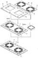
본 발명의 제1 실시예에 대해서, 제1도∼제5도를 참조하면서 설명한다.A first embodiment of the present invention will be described with reference to FIGS. 1 to 5.
제1도는 본 실시예의 반도체장치의 사시도이고, 제2도는 제1도의 중앙부분의 단면도이다. 제1도 및 제2도에 도시한 바와 같이, 금속판(6) 중앙의 구멍에는 반도체소자(1)이 장전되어 있고, 반도체소자(1) 주위의 금속판(6) 표면에는 배선패턴(4) 및 패드(5)를 갖는 절연테이프(테이프형상의 절연부재)(3)이 접착되어 있다. 이 배선패턴(4)의 재질로서는 예를 들면 동박을 사용한다. 배선패턴(4)의 한쪽(안쪽)은 절연테이프(3)의 내주에서 돌출되고 테이프 오토메이티드 본딩법에 의해 반도체소자(1)의 전극(2)에 전기적으로 접속되어 있고, 다른쪽은 땜납범프(8)을 접속하기 위한 패드(5)에 연결되어 있다. 금속판(6)은 배선패턴(4)나 패드(5)가 마련된 절연테이프(3)을 보강하는 역할을 하고 있으며, 금속판(6)의 외주는 절연테이프(3)의 외주보다 외측으로 돌출되어 있다. 또, 반도체소자(1)의 회로형성면 및 측면은 봉지수지(7)에 의해 봉지되어 있다. 단, 제1도에서는 구조를 알기 쉽게 표현하기 위해 봉지수지의 일부를 제외하여 도시하였다.FIG. 1 is a perspective view of the semiconductor device of this embodiment, and FIG. 2 is a sectional view of the central portion of FIG. As shown in FIG. 1 and FIG. 2, the
또, 상기 반도체장치의 측벽(1a)는 절단끝면으로서, 측벽(1a)에 있어서의 절연테이프(3), 접착제(20) 및 금속판(6)의 절단끝면이 일치하고, 절단에 수반되어 발생하는 끝면의 홈이 연속된 상태로 되어 있다(제5도 참조).The
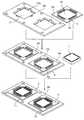
제1도 및 제2도에 도시한 본 실시예의 반도체장치의 제조공정을 제3도 및 제4도에 의해 설명한다. 우선, 제3도에 도시한 바와 같이, 반도체소자(1)을 수용하기 위한 여러개의 구멍(9a), (9b)(제3도에서는 2개)가 마련된 리이드프레임(9)에 배선패턴(4), 패드(5) 및 여러개의 반도체소자(1)를 수용하기 위한 여러개의 구멍(3a), (3b)가 마련된 절연테이프(3)을 접착한다. 이 절연테이프(3)은 장전할 여러개의 반도체소자(1)의 각각에 공통해서 연속된 1개의 테이프이다. 이 접착공정은 단순한 형상의 2종류의 판형상부재, 즉 리이드프레임(9)와 절연테이프(3)을 접착할 뿐이므로 경우에 따라서 예를 들면 프레스나 로울러등 다양한 방식으로 용이하게 접착을 실행할 수 있고, 접착제(20)의 두께를 균일하게 할 수 있으며 또한 테이프에 감기성질이 있는 경우에도 그의 감기성질을 제거하는 것도 용이하다.3 and 4 illustrate the manufacturing process of the semiconductor device of the present embodiment shown in FIGS. First, as shown in FIG. 3, the
다음에, 반도체소자(1)을 구멍(9a), (9b)에 장전하지만, 이 때 배선패턴(4)의 안쪽끝은 구멍(9a), (9b) 및 구멍(3a), (3b)의 내주에서 돌출되어 있으므로 반도체소자(1)은 배선패턴(4)의 안쪽끝을 파손하지 않도록 리이드프레임(9)의 하면쪽에서 구멍의 내부에 수용하는 것으로 한다. 계속해서, 배선패턴(4)와 반도체소자(1)의 전극(2)를 전기적으로 접속하지만, 본 실시예에서는 이 접속시에 테이프 오토메이티드 본딩법을 사용한다.Next, the
또, 제4도에 도시한 바와 같이, 봉지수지(7)에 의해 반도체소자(1)의 회로형성면과 측면을 봉지한다. 이 봉지시에는 통상의 테이프 캐리어 패키지에서 사용되고 있는 본딩법을 사용한다. 계속해서, 리이드프레임(9) 및 절연테이프(3)을 동일의 1점쇄선A-A를 따라 절단해서 개개의 반도체장치로 분할하고, 이것에 의해서 각 반도체장치에 대응하는 금속판(6)을 형성한다. 그리고, 마지막에 절연테이프(3)에 마련된 패드(4)에 땜납볼(10)을 접속하고, 땜납범프(8)로 한다.4, the circuit formation surface and the side surface of the
상기와 같은 공정에 의해 반도체장치를 제조하면, 최종적으로 리이드프레임(9)를 절단하여 개개의 반도체장치로 분할했을 때에는 상술한 바와 같이 그의 절단끝면이 측벽(1a)로 되고, 그 측벽(1a)에 있어서의 절연테이프(3), 접착제(20) 및 금속판(6)의 절단끝면이 일치하고, 제5도에 도시한 바와 같이 절단에 수반되어 생기는 끝면의 가공홈(30)이 연속된 상태로 된다.When the semiconductor device is manufactured by the above process, when the
이상과 같은 본 실시예에서는 절연테이프(3), 반도체소자(1), 봉지수지(7)등에 의한 개개의 반도체장치의 구성을 리이드프레임(9)에 형성하고 그 후에 분할하므로, 여러개의 반도체장치를 동시에 제조할 수 있으며 생산성을 현저히 향상시킬 수 있다. 또, 절연테이프(3)이 장전할 여러개의 반도체소자(1)의 각각에 공통해서 연속된 1장의 테이프이므로, 각 반도체소자(1)마다 개별의 절연테이프를 준비할 필요가 없고 절연테이프를 개별적으로 접착할 필요도 없어지므로 한층 생산성을 향상시킬 수 있다.In the present embodiment as described above, the structure of the individual semiconductor devices made of the insulating
또, 최초에 단순한 형상의 2종류의 판형상부재, 즉 리이드프레임(9)와 절연테이프(3)을 접착할 뿐이므로, 다양한 방식으로 용이하게 접착을 실행할 수 있고 접착제(20)의 두께를 균일하게 할 수 있으며 또한 절연테이프(3)의 감기성질을 제거하는 것도 용이하다. 따라서, 절연테이프(3)의 평탄도를 향상시키는 것이 가능하게 되고, 외부단자로서의 땜납범프(8)의 접속신뢰성을 향상시킬 수 있다.In addition, since only two kinds of plate-shaped members having a simple shape, that is, the
또, 본 실시예에서는 봉지수지(7)에 의한 봉지시에는 반도체장치가 개개로 분할되어 있지 않은 상태이므로, 본딩수지를 사용하지 않고 통상의 리이드를 갖는 패키지를 위해 사용되고 있는 트랜스퍼몰드법을 사용할 수 있다. 이것에 의해서도 생산성이 향상됨과 동시에 봉지의 신뢰성도 향상된다.In the present embodiment, since the semiconductor devices are not individually divided at the time of encapsulation by the
다음에, 본 발명의 제2 및 제3 실시예에 대해서 각각 제6도 및 제7도를 참조하면서 설명한다. 단, 제6도 및 제7도에 있어서 제1도∼제5도와 동등한 부재에는 동일부호를 붙이고 있다.Next, the second and third embodiments of the present invention will be described with reference to FIGS. 6 and 7, respectively. However, in Figs. 6 and 7, the same reference numerals are given to members that are the same as Figs.
제6도 및 제7도은 각각 봉지수지(7)에 의해 반도체소자(1)의 회로형성면 및 측면을 봉지하기 전의 상태를 도시한 도면이다. 제6도 및 제7도의 실시예에 있어서의 절연테이프로서는 제3도의 절연테이프(3)와 같이 반도체소자(1)의 각각에 공통해서 연속된 1장의 테이프로는 하지 않고, 각 반도체소자(1)에 대한 개별의 절연테이프(3A)로 한다. 도, 제7도에 도시한 제3 실시예에서는 분할시의 절단을 쉽게 하기 위해 리이드프레임(9c)에 미리 슬릿(13)이 마련되어 있다.6 and 7 show states before encapsulating the circuit forming surface and the side surface of the
그 이외의 반도체장치의 구성 및 제조공정은 제1 실시예와 동일하고, 이들 실시예에 있어서도 절연테이프(3A), 반도체소자(1), 봉지수지 등에 의한 개개의 반도체장치의 구성을 리이드프레임(9) 또는 (9c)에 형성하고, 그 후에 분할한다. 단, 각 절연테이프(3A)에 어느 정도의 간격이 마련되어 있으므로 개개의 반도체장치로 분할할 때에는 리이드프레임(9) 또는 (9c)만을 절단하게 된다. 따라서, 분할후의 반도체장치의 측벽에 있어서의 절연테이프(3A), 접착제 및 금속판의 절단끝면은 일치하지 않아 절단에 수반되어 생기는 끝면의 홈도 연속된 상태로는 되지 않는다.The structure and manufacturing process of the other semiconductor devices are the same as those in the first embodiment, and in these embodiments, the structure of the individual semiconductor devices made of the insulating
이들 제2 및 제3 실시예에 의하면, 각 반도체소자(1)마다 개별의 절연테이프를 준비하고 개별적으로 접착할 필요가 있지만, 그 이외는 제1 실시예와 거의 마찬가지의 효과가 얻어진다.According to these second and third embodiments, it is necessary to prepare separate insulating tapes for each
다음에, 본 발명의 제4 실시예에 대해서 제8도∼제10도를 참조하면서 설명한다. 단, 제8도∼제10도에 있어서 제1도∼제7도와 동등한 부재에는 동일부호를 붙이고 있다.Next, a fourth embodiment of the present invention will be described with reference to FIGS. However, in Figs. 8 to 10, the same reference numerals are given to members that are the same as Figs.
제8도는 본 실시예의 반도체장치의 사시도이고, 제9도는 제8도의 중앙부분의 단면도이다. 제8도 및 제9도에 도시한 바와 같이, 금속판(6) 중앙에는 관통하는 구멍이 없고, 금속판(6)과 일체의 소자탑재부(12)가 그의 중앙부에 마련되어 있다. 그리고, 금속판(6)의 소자탑재부(12)보다 외측은 절연테이프탑재부(12a)로 되어 있고 또한 소자탑재부(12) 상면은 절연테이프탑재부(12a) 표면보다 낮게 되어 있으며, 소자탑재부(12)와 절연테이프탑재부(12a) 사이는 연결용단차부(12b)에 의해 연결되어 있다. 또, 배선패턴(4) 안쪽은 반도체소자(1)의 전극(2)와 와이어(11)에 의해(와이어 본딩법을 사용해서) 접속되어 있다. 이 이외 그 밖의 구성은 제2 실시예와 동일하다. 단, 제8도에서는 구조를 알기쉽게 표현하기 위해 봉지수지의 일부를 제외해서 도시하였다.FIG. 8 is a perspective view of the semiconductor device of this embodiment, and FIG. 9 is a sectional view of the central portion of FIG. As shown in FIG. 8 and FIG. 9, there is no hole which penetrates in the center of the
제8도 및 제9도에 도시한 본 실시예의 반도체장치의 제조공정을 제10도에 의해 설명한다. 우선, 반도체소자(1)을 탑재하기 위한 여러개의(제3도에서는 2개)소자탑재부(12)가 마련된 리이드프레임(9A)에 배선패턴(4a), 패드(5) 및 여러개의 반도체소자(1)을 수용하기 위한 여러개의 구멍(3c)가 마련된 절연테이프(3A)를 접착한다. 단, 절연테이프(3A)는 제6도이나 제7도와 마찬가지로 각 반도체소자(1)에 대해 개별의 테이프로 하고 또 배선패턴(4a)는 절연테이프(3)의 표면내에만 존재하고 있고, 배선패턴(4a) 안쪽이 절연테이프(3)의 구멍(3c)로 돌출하지 않도록 되어 있다. 또, 연결용단차부(12b)는 소자탑재부(12)와 절연테이프탑재부(12a)의 경계보다 외측에서 시작되어 소자탑재부(12)의 외주에 이르는 형상으로 되어 있다. 이것에 의해 소자탑재부(12) 외주와 절연테이프탑재부(12a) 내주의 거리를 극력 짧게 하는 것이 가능하다.10 shows a manufacturing process of the semiconductor device of the present embodiment shown in FIG. 8 and FIG. First, a
다음에, 반도체소자(1)을 리이드프레임(9A)의 위쪽에서 소자탑재부(12)에 탑재하고 접착한다. 이 때, 배선패턴(4a)의 안쪽이 절연테이프(3)의 구멍(3c)로 돌출하지 않도록 되어 있으므로 반도체소자(1)을 리이드프레임(9A)의 위쪽에서 탑재해도 배선패턴(4a)를 파손하는 일이 없고 또 핸들링(조작)도 용이하게 된다. 또, 소자탑재부(12) 상면이 절연테이프탑재부(12a) 표면보다 낮게 되어 있으므로 반도체소자(1)이 절연테이프(3) 상면에서 돌출되는 것을 방지하는 것이 가능하게 된다. 다음에, 배선패턴(4a)와 반도체소자(1)의 전극(2)를 와이어(11)에 의해 전기적으로 접속한다. 이 이후의 제조공정은 제4도와 마찬가지이다.Next, the
상기에 있어서는 와이어본딩법을 사용하고 있지만, 이 방식은 최초에 리이드프레임(9A)와 절연테이프(3A)의 접착을 실행한다는 본 실시예의 독자의 구조에 의해 가능하게 된 것이다. 화이어본딩법에서는 열압착과 초음파접합을 병용해서 금속기리의 접합을 실행하지만, 이와 같은 작업을 실행하기 위해서는 접합하는 배선패턴의 강성이 높은 것이 필요하게 된다. 강성이 낮으면 접함면이 함몰되어 압착력이 전달되지 않거나 초음파가 흡수되어 접합할 수 없기 때문이다. 본 발명에서는 와이어본딩법에 의해 반도체소자(1)의 전극(2)와 배선패턴(4a)를 접속할 때에 절연테이프(3A)의 이면측에 이미 강성이 높은 리이드프레임(9A)가 접착되어 있으므로, 배선패턴(4a)의 강성도 높아지고 본딩시에 그들이 함몰하는 일이 없어 보다 접속신뢰성이 높은 와이어본딩법에 의해 안정된 접속을 실행할 수 있다. 또한, 상기 와이어본딩시에는 반도체소자(1)이 소자탑재부(12)상에 단단히 고정되어 있으므로 한층 확실하고 신뢰성이 있는 접속을 실행할 수 있다.Although the wire bonding method is used in the above, this method is made possible by the original structure of the present embodiment in which adhesion of the
또, 테이프캐리어패키지에서 사용되고 있는 테이프 오토메이티드 본딩을 사용하는 경우에는 특수한 제조장치가 필요하고, 또 반도체소자의 전극에 대한 배선패턴의 자유도가 전혀 없으므로 소자마다 테이프를 형성하지 않으면 안되지만, 본 발명에서는 보다 접속신뢰성이 높은 와이어본딩법에 의해 접속할 수 있다는 점에서 유리하다.In the case where the tape automated bonding used in the tape carrier package is used, a special manufacturing apparatus is required, and since there is no freedom of wiring patterns with respect to the electrodes of the semiconductor elements, a tape must be formed for each element. It is advantageous in that connection can be made by a wire bonding method with higher connection reliability.
이상과 같은 본 실시예에 의하면, 절연테이프(3A)의 이면측에 강성이 높은 리이드프레임(9A)를 접착하므로, 배선패턴(4a)의 강성을 향상시킬 수 있으며 보다 접속신뢰성이 높은 와이어본딩법에 의해 안정된 접속을 실행할 수 있다. 또한, 반도체소자(1)이 소자탑재부(12)상에 단단히 고정되어 있으므로 더욱더 확실하고 신뢰성 있는 접속을 실행할 수 있다.According to the present embodiment as described above, since the
또, 소자탑재부(12) 상면이 절연테이프탑재부(12a) 표면보다 낮게 되어 있으므로, 반도체소자(1)의 탑재시에 그 반도체소자(1)이 절연테이프(3) 상면에서 돌출되는 것을 방지할 수 있다.In addition, since the upper surface of the
또, 연결용단차부(12b)를 상기와 같은 형상으로 하므로, 소자탑재부(12) 외주와 절연테이프탑재부(12a) 내주의 거리를 극력 짧게 하는 것이 가능하다.In addition, since the
다음에, 본 발명의 제5 실시예에 대해서 제11도 및 제12도를 참조하면서 설명한다. 단, 제11도 및 제12도에 있어서, 제1도∼제7도와 동등한 부재에는 동일부호를 붙이고 있다.Next, a fifth embodiment of the present invention will be described with reference to FIGS. 11 and 12. FIG. 11 and 12, the same reference numerals are assigned to members that are the same as in FIGS.
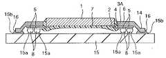
제11도는 본 실시예의 반도체장치의 사시도이고, 제12도는 제11도의 반도체장치를 프린트기판에 실장했을 때의 중앙부분의 단면도이다. 제11도 및 제12도에 도시한 바와 같이, 본 실시예의 반도체장치에 있어서는 금속판(6)의 외주에 금속판(6) 표면보다 위쪽으로 돌출된 돌기리이드(14)가 마련되어 있다. 이 돌기리이드(14)는 땜납범프(8)의 상면을 포함하는 평면내까지 즉 땜납범프(8)의 높이의 위치까지 돌출되어 있다. 이 이외 그 밖의 구성은 제2 실시예와 마찬가지이다. 단, 제11도에서는 구조를 알기쉽게 표현하기 위해 봉지수지의 일부를 제외해서 도시하였다.FIG. 11 is a perspective view of the semiconductor device of this embodiment, and FIG. 12 is a sectional view of the central portion when the semiconductor device of FIG. 11 is mounted on a printed board. As shown in Figs. 11 and 12, in the semiconductor device of the present embodiment, the
이 반도체장치가 프린트기판에 실장될 때에는 제12도에 도시한 바와 같이, 프린트기판(15)의 전극(15a)에 땜납범프(8)이 접합되고, 또 프린트기판(15)의 돌기 리이드접합부(15b)에 돌리리이드(14)의 선단이 땜납(16)을 거쳐서 접합된다. 또, 돌기리이드접합부(15b)는 접지에 접속된다.When the semiconductor device is mounted on a printed board, as shown in FIG. 12, the solder bumps 8 are bonded to the
이와 같은 구성의 반도체장치는 프린트기판에 실장하는 것에 의해 다음의 2가지의 효과가 있다.The semiconductor device having such a structure has the following two effects by being mounted on a printed board.
하나는 전기적특성의 향상이다. 금속판(6)이 배선패턴(4)와 매우 가까운 위치에 절연되어 존재하고 있으므로 금속판(6)과 일체의 돌기리이드(14)를 접지에 접속된 돌기리이드접합부(15b)와 접합하면 접지면(grand plane)으로서 기능시킬 수 있고, 반도체장치에서 생기는 전기적노이즈를 저감할 수 있으며 탑재하는 바도체소자(1)을 동작주파수가 높은 것으로 할 수 있다.One is the improvement of electrical characteristics. Since the
또 다른 하나는 반도체장치에서 프린트기판으로 방출하는 열저항의 저감이다. 반도체소자(1)에서 봉지수지(7), 금속판(6)을 통과하여 돌기리이드(14)를 거쳐서 프린트기판(15)상의 돌기리이드접합부(15b)에 이르는 방열경로가 형성되므로 반도체소자(1)에서 발생하는 열을 효율적으로 방출할 수 있어 열저항을 저감하는 것이 가능하게 되고 또한 높은 발열량을 갖는 반도체소자(1)의 탑재도 가능하다.Another is the reduction of the thermal resistance emitted from the semiconductor device to the printed circuit board. Since the heat dissipation path from the
다음에, 본 발명의 제6 실시예데 대해서 제13도에 의해 설명한다. 본 실시예는 제13도에 도시한 바와 같이, 제4 실시예의 반도체장치에 있어서의 금속판(6)의 외주에 제5 실시예와 마찬가지의 돌기리이드(14)를 마련한 것이다. 이 이외 그 밖의 구성은 제4 실시예와 마찬가지이고, 제13도에 있어서 제8도 또는 제11도와 동등한 부재에는 동일부호를 붙이고 있다.Next, a sixth embodiment of the present invention will be described with reference to FIG. In the present embodiment, as shown in FIG. 13, the
본 실시예에 의하면, 반도체소자(1)과 프린트기판(15)의 돌기리이드접합부(15b)가 금속판(6)을 거쳐서 접속되게 되므로, 특히 상술한 제5 실시예에 비해 방열효과는 더욱 향상한다.According to the present embodiment, the
또한, 이상 6개의 실시예에서는 간단하게 하기 위해 2개의 반도체소자를 1장의 리이드프레임에 장전하는 예를 설명하였지만, 탑재하는 반도체소자의 수를 많게 하는 것은 물론 가능하고, 그 수가 많으면 많을수록 생산성이 향상되는 것은 물론이다. 또, 반도체소자를 리이드프레임에 여러행 여러열의 매트릭스형상으로 장전하면 한층 더 효율적이다.In the above six embodiments, for the sake of simplicity, an example in which two semiconductor devices are loaded in one lead frame has been described. However, it is possible to increase the number of semiconductor devices to be mounted, and the larger the number, the higher the productivity. Of course it becomes. In addition, it is more efficient if the semiconductor element is loaded into a lead frame in a matrix form of several rows and columns.
본 발명에 의하면, 개개의 반도체장치의 구성을 리이드프레임에 형성하고나서 분할하므로 여러개의 반도체패키지를 동시에 제조할 수 있고 생산성을 향상시키는 것이 가능하게된다. 또, 최초에 단순한 형상의 리이드프레임과 절연테이프를 접착할 뿐이므로 용이하게 접착을 실행하는 것이 가능하고 접착제의 두께를 균일하게 할 수 있으며 절연테이프의 평탄도를 향상시켜서 땜납범프의 접속신뢰성을 향상시킬 수 있다.According to the present invention, since the structure of each semiconductor device is formed in the lead frame and then divided, it is possible to manufacture several semiconductor packages at the same time and to improve productivity. In addition, since the lead frame and the insulating tape of simple shape are first adhered to each other, the adhesion can be easily performed, the thickness of the adhesive can be made uniform, and the flatness of the insulating tape is improved to improve the solder bump connection reliability. You can.
Claims (12)
Translated fromKoreanApplications Claiming Priority (3)
| Application Number | Priority Date | Filing Date | Title |
|---|---|---|---|
| JP30956696AJP3612155B2 (en) | 1996-11-20 | 1996-11-20 | Semiconductor device and lead frame for semiconductor device |
| JP96-309566 | 1996-11-20 | ||
| JP08-309566 | 1996-11-20 |
Publications (2)
| Publication Number | Publication Date |
|---|---|
| KR19980042513A KR19980042513A (en) | 1998-08-17 |
| KR100274854B1true KR100274854B1 (en) | 2000-12-15 |
Family
ID=17994574
Family Applications (1)
| Application Number | Title | Priority Date | Filing Date |
|---|---|---|---|
| KR1019970060650AExpired - Fee RelatedKR100274854B1 (en) | 1996-11-20 | 1997-11-17 | Lead frame for semiconductor device and semiconductor device |
Country Status (4)
| Country | Link |
|---|---|
| US (2) | US6465876B1 (en) |
| JP (1) | JP3612155B2 (en) |
| KR (1) | KR100274854B1 (en) |
| TW (1) | TW381326B (en) |
Families Citing this family (11)
| Publication number | Priority date | Publication date | Assignee | Title |
|---|---|---|---|---|
| JP3512655B2 (en)* | 1998-12-01 | 2004-03-31 | シャープ株式会社 | Semiconductor device, method of manufacturing the same, and reinforcing tape used for manufacturing the semiconductor device |
| US6975021B1 (en)* | 1999-09-03 | 2005-12-13 | Micron Technology, Inc. | Carrier for substrate film |
| TW563232B (en)* | 2002-08-23 | 2003-11-21 | Via Tech Inc | Chip scale package and method of fabricating the same |
| JP3751938B2 (en)* | 2002-12-09 | 2006-03-08 | 日東電工株式会社 | TAB tape carrier and method for manufacturing the same |
| CN1322581C (en)* | 2003-07-28 | 2007-06-20 | 日月光半导体制造股份有限公司 | Substrate for semiconductor package structure |
| US8129225B2 (en)* | 2007-08-10 | 2012-03-06 | Infineon Technologies Ag | Method of manufacturing an integrated circuit module |
| JP5407474B2 (en)* | 2009-03-25 | 2014-02-05 | 凸版印刷株式会社 | Manufacturing method of semiconductor element substrate |
| US8133759B2 (en)* | 2009-04-28 | 2012-03-13 | Macronix International Co., Ltd. | Leadframe |
| US9029991B2 (en)* | 2010-11-16 | 2015-05-12 | Conexant Systems, Inc. | Semiconductor packages with reduced solder voiding |
| US9978707B1 (en)* | 2017-03-23 | 2018-05-22 | Delphi Technologies, Inc. | Electrical-device adhesive barrier |
| CN111438444B (en)* | 2018-12-28 | 2022-08-12 | 北京北科天绘科技有限公司 | A laser cutting method and system based on mass transfer of device arrays |
Citations (1)
| Publication number | Priority date | Publication date | Assignee | Title |
|---|---|---|---|---|
| JPH0878574A (en)* | 1994-09-08 | 1996-03-22 | Shinko Electric Ind Co Ltd | Semiconductor device and manufacturing method thereof |
Family Cites Families (11)
| Publication number | Priority date | Publication date | Assignee | Title |
|---|---|---|---|---|
| US5023202A (en)* | 1989-07-14 | 1991-06-11 | Lsi Logic Corporation | Rigid strip carrier for integrated circuits |
| KR100192871B1 (en)* | 1989-09-28 | 1999-06-15 | 기타지마 요시도시 | Semiconductor device having a leadframe and metal substrate |
| US5148265A (en) | 1990-09-24 | 1992-09-15 | Ist Associates, Inc. | Semiconductor chip assemblies with fan-in leads |
| US5216278A (en) | 1990-12-04 | 1993-06-01 | Motorola, Inc. | Semiconductor device having a pad array carrier package |
| JP2826049B2 (en) | 1992-11-18 | 1998-11-18 | 松下電子工業株式会社 | Semiconductor device and manufacturing method thereof |
| JPH06209054A (en) | 1993-01-08 | 1994-07-26 | Mitsubishi Electric Corp | Semiconductor device |
| JP3057130B2 (en) | 1993-02-18 | 2000-06-26 | 三菱電機株式会社 | Resin-sealed semiconductor package and method of manufacturing the same |
| US5656550A (en)* | 1994-08-24 | 1997-08-12 | Fujitsu Limited | Method of producing a semicondutor device having a lead portion with outer connecting terminal |
| JPH0888293A (en) | 1994-09-19 | 1996-04-02 | Mitsui High Tec Inc | Semiconductor mounting device and mounting method for semiconductor device using the same |
| US5661086A (en)* | 1995-03-28 | 1997-08-26 | Mitsui High-Tec, Inc. | Process for manufacturing a plurality of strip lead frame semiconductor devices |
| US5663530A (en)* | 1995-08-01 | 1997-09-02 | Minnesota Mining And Manufacturing Company | Wire bond tape ball grid array package |
- 1996
- 1996-11-20JPJP30956696Apatent/JP3612155B2/ennot_activeExpired - Fee Related
- 1997
- 1997-11-17KRKR1019970060650Apatent/KR100274854B1/ennot_activeExpired - Fee Related
- 1997-11-18TWTW86117214Apatent/TW381326B/ennot_activeIP Right Cessation
- 1997-11-19USUS08/974,682patent/US6465876B1/ennot_activeExpired - Fee Related
- 2002
- 2002-05-02USUS10/136,409patent/US6844219B2/ennot_activeExpired - Fee Related
Patent Citations (1)
| Publication number | Priority date | Publication date | Assignee | Title |
|---|---|---|---|---|
| JPH0878574A (en)* | 1994-09-08 | 1996-03-22 | Shinko Electric Ind Co Ltd | Semiconductor device and manufacturing method thereof |
Also Published As
| Publication number | Publication date |
|---|---|
| US6465876B1 (en) | 2002-10-15 |
| US20020135051A1 (en) | 2002-09-26 |
| KR19980042513A (en) | 1998-08-17 |
| TW381326B (en) | 2000-02-01 |
| JPH10150072A (en) | 1998-06-02 |
| US6844219B2 (en) | 2005-01-18 |
| JP3612155B2 (en) | 2005-01-19 |
Similar Documents
| Publication | Publication Date | Title |
|---|---|---|
| US7115442B2 (en) | Ball grid array package with stacked center pad chips and method for manufacturing the same | |
| KR100324333B1 (en) | Stacked package and fabricating method thereof | |
| KR100204753B1 (en) | ELC Type Stacked Chip Package | |
| KR970006533B1 (en) | Semiconductor device and manufacturing method | |
| JPH10200012A (en) | Package of ball grid array semiconductor and its manufacturing method | |
| KR20030018642A (en) | Stack chip module | |
| KR20050077866A (en) | Semiconductor package with heat-dissipating structure and method for fabricating the same | |
| KR100265566B1 (en) | Ship stack package | |
| JP2000307045A (en) | Lead frame and manufacture of resin sealed semiconductor device using it | |
| KR100274854B1 (en) | Lead frame for semiconductor device and semiconductor device | |
| JP3072291B1 (en) | Lead frame, resin-encapsulated semiconductor device using the same and method of manufacturing the same | |
| US6903464B2 (en) | Semiconductor die package | |
| US5808872A (en) | Semiconductor package and method of mounting the same on circuit board | |
| KR19990069447A (en) | Semiconductor package and manufacturing method | |
| KR100422608B1 (en) | Stack chip package | |
| KR100291511B1 (en) | Multi-chip package | |
| KR20000035215A (en) | Semiconductor device and method of producing same | |
| KR20000006597A (en) | Plastic package having an air cavity and method thereof | |
| KR100388291B1 (en) | Structure of semiconductor package | |
| JP3127948B2 (en) | Semiconductor package and mounting method thereof | |
| KR200159861Y1 (en) | Semiconductor package | |
| KR100379092B1 (en) | semiconductor package and its manufacturing method | |
| KR100324932B1 (en) | chip size package | |
| JP3474408B2 (en) | Semiconductor device and manufacturing method thereof | |
| CN120711798A (en) | A power module packaging structure and power module |
Legal Events
| Date | Code | Title | Description |
|---|---|---|---|
| A201 | Request for examination | ||
| PA0109 | Patent application | St.27 status event code:A-0-1-A10-A12-nap-PA0109 | |
| PA0201 | Request for examination | St.27 status event code:A-1-2-D10-D11-exm-PA0201 | |
| R17-X000 | Change to representative recorded | St.27 status event code:A-3-3-R10-R17-oth-X000 | |
| PG1501 | Laying open of application | St.27 status event code:A-1-1-Q10-Q12-nap-PG1501 | |
| R18-X000 | Changes to party contact information recorded | St.27 status event code:A-3-3-R10-R18-oth-X000 | |
| PN2301 | Change of applicant | St.27 status event code:A-3-3-R10-R13-asn-PN2301 St.27 status event code:A-3-3-R10-R11-asn-PN2301 | |
| E902 | Notification of reason for refusal | ||
| PE0902 | Notice of grounds for rejection | St.27 status event code:A-1-2-D10-D21-exm-PE0902 | |
| T11-X000 | Administrative time limit extension requested | St.27 status event code:U-3-3-T10-T11-oth-X000 | |
| P11-X000 | Amendment of application requested | St.27 status event code:A-2-2-P10-P11-nap-X000 | |
| P13-X000 | Application amended | St.27 status event code:A-2-2-P10-P13-nap-X000 | |
| E701 | Decision to grant or registration of patent right | ||
| PE0701 | Decision of registration | St.27 status event code:A-1-2-D10-D22-exm-PE0701 | |
| GRNT | Written decision to grant | ||
| PR0701 | Registration of establishment | St.27 status event code:A-2-4-F10-F11-exm-PR0701 | |
| PR1002 | Payment of registration fee | St.27 status event code:A-2-2-U10-U11-oth-PR1002 Fee payment year number:1 | |
| PG1601 | Publication of registration | St.27 status event code:A-4-4-Q10-Q13-nap-PG1601 | |
| PR1001 | Payment of annual fee | St.27 status event code:A-4-4-U10-U11-oth-PR1001 Fee payment year number:4 | |
| PR1001 | Payment of annual fee | St.27 status event code:A-4-4-U10-U11-oth-PR1001 Fee payment year number:5 | |
| R18-X000 | Changes to party contact information recorded | St.27 status event code:A-5-5-R10-R18-oth-X000 | |
| PR1001 | Payment of annual fee | St.27 status event code:A-4-4-U10-U11-oth-PR1001 Fee payment year number:6 | |
| PR1001 | Payment of annual fee | St.27 status event code:A-4-4-U10-U11-oth-PR1001 Fee payment year number:7 | |
| PR1001 | Payment of annual fee | St.27 status event code:A-4-4-U10-U11-oth-PR1001 Fee payment year number:8 | |
| PR1001 | Payment of annual fee | St.27 status event code:A-4-4-U10-U11-oth-PR1001 Fee payment year number:9 | |
| FPAY | Annual fee payment | Payment date:20090910 Year of fee payment:10 | |
| PR1001 | Payment of annual fee | St.27 status event code:A-4-4-U10-U11-oth-PR1001 Fee payment year number:10 | |
| LAPS | Lapse due to unpaid annual fee | ||
| PC1903 | Unpaid annual fee | St.27 status event code:A-4-4-U10-U13-oth-PC1903 Not in force date:20100919 Payment event data comment text:Termination Category : DEFAULT_OF_REGISTRATION_FEE | |
| PC1903 | Unpaid annual fee | St.27 status event code:N-4-6-H10-H13-oth-PC1903 Ip right cessation event data comment text:Termination Category : DEFAULT_OF_REGISTRATION_FEE Not in force date:20100919 |