KR100272752B1 - Vapor phase growth apparatus and vapor phase growth method - Google Patents
Vapor phase growth apparatus and vapor phase growth methodDownload PDFInfo
- Publication number
- KR100272752B1 KR100272752B1KR1019970708329AKR19970708329AKR100272752B1KR 100272752 B1KR100272752 B1KR 100272752B1KR 1019970708329 AKR1019970708329 AKR 1019970708329AKR 19970708329 AKR19970708329 AKR 19970708329AKR 100272752 B1KR100272752 B1KR 100272752B1
- Authority
- KR
- South Korea
- Prior art keywords
- gas
- substrate
- phase growth
- growth
- vapor phase
- Prior art date
- Legal status (The legal status is an assumption and is not a legal conclusion. Google has not performed a legal analysis and makes no representation as to the accuracy of the status listed.)
- Expired - Fee Related
Links
Images


Classifications
- H01L21/205—
- C—CHEMISTRY; METALLURGY
- C23—COATING METALLIC MATERIAL; COATING MATERIAL WITH METALLIC MATERIAL; CHEMICAL SURFACE TREATMENT; DIFFUSION TREATMENT OF METALLIC MATERIAL; COATING BY VACUUM EVAPORATION, BY SPUTTERING, BY ION IMPLANTATION OR BY CHEMICAL VAPOUR DEPOSITION, IN GENERAL; INHIBITING CORROSION OF METALLIC MATERIAL OR INCRUSTATION IN GENERAL
- C23C—COATING METALLIC MATERIAL; COATING MATERIAL WITH METALLIC MATERIAL; SURFACE TREATMENT OF METALLIC MATERIAL BY DIFFUSION INTO THE SURFACE, BY CHEMICAL CONVERSION OR SUBSTITUTION; COATING BY VACUUM EVAPORATION, BY SPUTTERING, BY ION IMPLANTATION OR BY CHEMICAL VAPOUR DEPOSITION, IN GENERAL
- C23C16/00—Chemical coating by decomposition of gaseous compounds, without leaving reaction products of surface material in the coating, i.e. chemical vapour deposition [CVD] processes
- C23C16/44—Chemical coating by decomposition of gaseous compounds, without leaving reaction products of surface material in the coating, i.e. chemical vapour deposition [CVD] processes characterised by the method of coating
- C23C16/455—Chemical coating by decomposition of gaseous compounds, without leaving reaction products of surface material in the coating, i.e. chemical vapour deposition [CVD] processes characterised by the method of coating characterised by the method used for introducing gases into reaction chamber or for modifying gas flows in reaction chamber
- C23C16/45514—Mixing in close vicinity to the substrate
- C—CHEMISTRY; METALLURGY
- C23—COATING METALLIC MATERIAL; COATING MATERIAL WITH METALLIC MATERIAL; CHEMICAL SURFACE TREATMENT; DIFFUSION TREATMENT OF METALLIC MATERIAL; COATING BY VACUUM EVAPORATION, BY SPUTTERING, BY ION IMPLANTATION OR BY CHEMICAL VAPOUR DEPOSITION, IN GENERAL; INHIBITING CORROSION OF METALLIC MATERIAL OR INCRUSTATION IN GENERAL
- C23C—COATING METALLIC MATERIAL; COATING MATERIAL WITH METALLIC MATERIAL; SURFACE TREATMENT OF METALLIC MATERIAL BY DIFFUSION INTO THE SURFACE, BY CHEMICAL CONVERSION OR SUBSTITUTION; COATING BY VACUUM EVAPORATION, BY SPUTTERING, BY ION IMPLANTATION OR BY CHEMICAL VAPOUR DEPOSITION, IN GENERAL
- C23C16/00—Chemical coating by decomposition of gaseous compounds, without leaving reaction products of surface material in the coating, i.e. chemical vapour deposition [CVD] processes
- C23C16/44—Chemical coating by decomposition of gaseous compounds, without leaving reaction products of surface material in the coating, i.e. chemical vapour deposition [CVD] processes characterised by the method of coating
- C23C16/455—Chemical coating by decomposition of gaseous compounds, without leaving reaction products of surface material in the coating, i.e. chemical vapour deposition [CVD] processes characterised by the method of coating characterised by the method used for introducing gases into reaction chamber or for modifying gas flows in reaction chamber
- C23C16/45587—Mechanical means for changing the gas flow
- C23C16/45591—Fixed means, e.g. wings, baffles
- C—CHEMISTRY; METALLURGY
- C30—CRYSTAL GROWTH
- C30B—SINGLE-CRYSTAL GROWTH; UNIDIRECTIONAL SOLIDIFICATION OF EUTECTIC MATERIAL OR UNIDIRECTIONAL DEMIXING OF EUTECTOID MATERIAL; REFINING BY ZONE-MELTING OF MATERIAL; PRODUCTION OF A HOMOGENEOUS POLYCRYSTALLINE MATERIAL WITH DEFINED STRUCTURE; SINGLE CRYSTALS OR HOMOGENEOUS POLYCRYSTALLINE MATERIAL WITH DEFINED STRUCTURE; AFTER-TREATMENT OF SINGLE CRYSTALS OR A HOMOGENEOUS POLYCRYSTALLINE MATERIAL WITH DEFINED STRUCTURE; APPARATUS THEREFOR
- C30B25/00—Single-crystal growth by chemical reaction of reactive gases, e.g. chemical vapour-deposition growth
- C30B25/02—Epitaxial-layer growth
- C30B25/14—Feed and outlet means for the gases; Modifying the flow of the reactive gases
- C—CHEMISTRY; METALLURGY
- C30—CRYSTAL GROWTH
- C30B—SINGLE-CRYSTAL GROWTH; UNIDIRECTIONAL SOLIDIFICATION OF EUTECTIC MATERIAL OR UNIDIRECTIONAL DEMIXING OF EUTECTOID MATERIAL; REFINING BY ZONE-MELTING OF MATERIAL; PRODUCTION OF A HOMOGENEOUS POLYCRYSTALLINE MATERIAL WITH DEFINED STRUCTURE; SINGLE CRYSTALS OR HOMOGENEOUS POLYCRYSTALLINE MATERIAL WITH DEFINED STRUCTURE; AFTER-TREATMENT OF SINGLE CRYSTALS OR A HOMOGENEOUS POLYCRYSTALLINE MATERIAL WITH DEFINED STRUCTURE; APPARATUS THEREFOR
- C30B29/00—Single crystals or homogeneous polycrystalline material with defined structure characterised by the material or by their shape
- C30B29/10—Inorganic compounds or compositions
- C30B29/40—AIIIBV compounds wherein A is B, Al, Ga, In or Tl and B is N, P, As, Sb or Bi
- C30B29/403—AIII-nitrides
- C30B29/406—Gallium nitride
- C—CHEMISTRY; METALLURGY
- C30—CRYSTAL GROWTH
- C30B—SINGLE-CRYSTAL GROWTH; UNIDIRECTIONAL SOLIDIFICATION OF EUTECTIC MATERIAL OR UNIDIRECTIONAL DEMIXING OF EUTECTOID MATERIAL; REFINING BY ZONE-MELTING OF MATERIAL; PRODUCTION OF A HOMOGENEOUS POLYCRYSTALLINE MATERIAL WITH DEFINED STRUCTURE; SINGLE CRYSTALS OR HOMOGENEOUS POLYCRYSTALLINE MATERIAL WITH DEFINED STRUCTURE; AFTER-TREATMENT OF SINGLE CRYSTALS OR A HOMOGENEOUS POLYCRYSTALLINE MATERIAL WITH DEFINED STRUCTURE; APPARATUS THEREFOR
- C30B29/00—Single crystals or homogeneous polycrystalline material with defined structure characterised by the material or by their shape
- C30B29/10—Inorganic compounds or compositions
- C30B29/40—AIIIBV compounds wherein A is B, Al, Ga, In or Tl and B is N, P, As, Sb or Bi
- C30B29/42—Gallium arsenide
Landscapes
- Chemical & Material Sciences (AREA)
- Engineering & Computer Science (AREA)
- Materials Engineering (AREA)
- Metallurgy (AREA)
- Organic Chemistry (AREA)
- Crystallography & Structural Chemistry (AREA)
- General Chemical & Material Sciences (AREA)
- Chemical Kinetics & Catalysis (AREA)
- Inorganic Chemistry (AREA)
- Mechanical Engineering (AREA)
- Chemical Vapour Deposition (AREA)
Abstract
Translated fromKoreanDescription
Translated fromKorean기판을 설치한 반응관내에 원료가스를 도입하여 기판면에 화합물 반도체박막을 형성하는 횡형 기상성장장치로서 예컨대 일본국 특공평 7-27868호 공보에 기재된 장치가 알려져 있다.BACKGROUND ART For example, the apparatus described in Japanese Patent Application Laid-Open No. 7-27868 is known as a horizontal vapor phase growth apparatus for introducing a raw material gas into a reaction tube provided with a substrate to form a compound semiconductor thin film on the substrate surface.
상기 공보에 개시된 기상성장장치는, 원통형상의 반응관을 축선을 수평방향으로 하여 설치하고, 상기 반응관내의 하부에 기판을 유지하는 서셉터(유지대)를 설치하고 있다. 상기 반응관은, 반응관의 기판설치부 상류쪽에 상기 기판 표면과 평행하게 칸막이판을 배설하고, 상기 칸막이판 상하에 두개의 평행한 유로, 즉 기판설치부쪽의 하부유로와 기판설치부 반대쪽의 상부유로를 구획형성하고 있다. 반응관의 기판설치부 하류쪽에는 가스배출관이 설치되어 있다. 상기 반응관내의 상기 서셉터 상류쪽에는, 가스의 흐름을 원활하게 하기 위한 플로우채널이 설치되어 있다. 상기 반응관의 기판설치부의 바깥둘레에는 가열용 RF코일이 배치되어 있다.In the gas phase growth apparatus disclosed in the above publication, a cylindrical reaction tube is provided with an axis in a horizontal direction, and a susceptor (holding zone) for holding a substrate is provided below the reaction tube. The reaction tube has a partition plate disposed upstream of the substrate mounting portion of the reaction tube in parallel with the surface of the substrate, and two parallel flow paths above and below the partition plate, namely, a lower flow path on the substrate mounting portion and an upper portion opposite the substrate mounting portion. The flow path is partitioned. A gas discharge pipe is installed downstream of the substrate mounting portion of the reaction tube. On the upstream side of the susceptor in the reaction tube, a flow channel for smoothing the flow of gas is provided. An RF coil for heating is disposed on the outer circumference of the substrate mounting portion of the reaction tube.
상기 기상성장장치는, 서셉터상에 재치된 기판을 RF코일로 가열한 상태에서 상기 상부유로에 원료가스를 희석가스로 희석한 기상성장가스를 도입함과 동시에, 하부유로에 원료가스를 포함하지 않은 개재가스를 도입하여 기상성장을 행한다. 이 개재가스로서는, 기상성장가스중의 희석가스와 같은 가스 또는 이것에 소량의 휘발억제가스를 첨가한 것을 사용하고 있다.The vapor phase growth apparatus introduces a vapor phase growth gas obtained by diluting the raw material gas with a dilution gas to the upper flow path while the substrate placed on the susceptor is heated with an RF coil, and does not include the raw material gas in the lower flow path. Gas phase growth is performed by introducing an intervening gas. As the interposition gas, a gas such as a dilution gas in the gaseous growth gas or a gas in which a small amount of volatilization inhibiting gas is added is used.
상기 상부유로로 흐르는 기상성장가스와 상기 하부유로로 흐르는 개재가스는, 상기 칸막이판의 앞끝단에서 상기 기판을 향하여 흐르고, 가스의 상호 확산작용에 의해 기상성장가스중의 원료가스가 개재가스중에 확산되고, 개재가스중의 원료가스의 농도가 서서히 높아지면서 기판 표면에 접근한다. 그리고, 개재가스중의 원료가스가 기판근방의 고온부에서 열분해하고, 기판 표면상에 퇴적하여 기판 표면에 성장막이 형성된다.The gaseous growth gas flowing into the upper flow passage and the intervening gas flowing into the lower flow passage flow toward the substrate at the front end of the partition plate, and the source gas in the gaseous growth gas diffuses into the interposition gas by the mutual diffusion of the gases. As a result, the concentration of the source gas in the intervening gas gradually increases to approach the substrate surface. The source gas in the interposition gas is thermally decomposed at a high temperature portion near the substrate, and is deposited on the substrate surface to form a growth film on the substrate surface.
이 때, 개재가스 및 기상성장가스의 각 유속과 기상성장가스중의 원료가스농도를 적절하게 조절함으로써 기상성장가스에서 개재가스중으로 확산하는 원료가스량과 기판 표면으로의 퇴적에 의해 개재가스에서 소실하는 원료가스량을 단위시간당으로 균일하게 유지할 수 있고, 기판 표면통과시의 개재가스중의 원료가스농도를 흐르는 방향으로 균일한 농도분포로 하여 균일한 막두께의 성장막을 형성할 수 있다.At this time, by appropriately adjusting the flow rates of the intervening gas and the gaseous growth gas and the concentration of the raw material gas in the gaseous growth gas, the amount of the raw material gas diffused from the gaseous growth gas into the intervening gas and the gas lost due to deposition on the substrate surface The amount of raw material gas can be maintained uniformly per unit time, and a growth film having a uniform film thickness can be formed with a uniform concentration distribution in the direction of flowing the raw material gas concentration in the intervening gas at the time of passage of the substrate surface.
이와 같이, 상기 횡형 기상성장장치는, 칸막이판에 의해 기상성장가스와 개재가스를 2층으로 흐르게 하여 따로따로 도입하고, 기상성장가스중의 원료가스를 개재가스중에 확산시켜서 기판 표면에 도달시킴으로써, 균일한 막두께의 성막기판을 얻을 수 있음과 동시에, 개재가스의 존재에 의해 원료가스농도가 낮은 상태에서 기판 표면위로 흐르므로, 기판이외로의 유해퇴적물양을 감소시킬 수 있다.As described above, the lateral gas phase growth apparatus introduces the gas phase growth gas and the intervening gas into two layers by a partition plate, and introduces them separately, diffuses the source gas in the gas phase growth gas into the interposition gas, and reaches the substrate surface. A film formation substrate having a uniform film thickness can be obtained and the amount of harmful deposits outside the substrate can be reduced since the presence of the intervening gas flows on the substrate surface at a low raw gas concentration.
그러나, 상기 횡형 기상성장장치에서 이성분계 이상의 성장막을 형성하면, 복수종류의 성분원소 내에 휘발성이 높은 원소가 성장막에서 증발하여 성장막에 결함을 발생시키는 일이 있다. 이 결함의 발생을 방지하기 위해 종래에는 휘발성이 높은 원소를 포함한 원료가스(휘발성가스)를 상기 휘발성가스의 평형분압 이상으로 많이 공급하는 등의 대책을 강구했지만, 원료의 이용효율 저하등에 따라 비용의 상승을 초래하였다.However, when a growth film of two or more components is formed in the lateral vapor phase growth apparatus, elements having high volatility within a plurality of kinds of component elements may evaporate from the growth film and cause defects in the growth film. In order to prevent the occurrence of this defect, conventionally, measures such as supplying a large amount of raw material gas (volatile gas) containing highly volatile elements above the equilibrium partial pressure of the volatile gas have been taken. It caused an increase.
또, 기판 표면위에 원하는 반응생성물을 퇴적시키기 위해서는, 가스의 유속을 최적의 상태로 조절할 필요가 있지만, 가스의 유속조절은 원료의 이용효율과 디바이스 제조공정에 필요한 불순물 도핑등도 포함시켜 미묘한 조정이 필요하고, 종래의 횡형 기상성장장치에서는, 복잡한 구조의 디바이스용 박막을 막두께와 조성, 도핑의 균일성을 동시에 만족시켜서 제작하는 것은 곤란하였다.In addition, in order to deposit a desired reaction product on the surface of the substrate, it is necessary to adjust the flow rate of the gas to an optimum state, but the control of the flow rate of the gas includes subtle adjustments including the doping of the raw materials and the doping of impurities necessary for the device manufacturing process. In the conventional horizontal vapor phase growth apparatus, it was difficult to produce a thin film for a device having a complicated structure while satisfying the film thickness, composition, and uniformity of doping simultaneously.
즉, 종래는, 원료가스농도를 조정하여 휘발성분의 휘발방지를 도모하고, 가스유속을 조정하여 반응생성물의 퇴적 존을 기판면 위에 일치시키기도 했지만, 균일한 막두께를 얻기 위한 조건과 원료가스농도의 최적 조건이 반드시 양호한 성막특성을 얻는 조건과는 일치하지 않는 경우가 있다. 또, 막두께의 균일성과 도핑의 균일성을 얻을 수 있는 가스유속의 최적조건이 일치하지 않는 일도 있기 때문에, 가스유속을 조절하는 방법으로는, 디바이스용 등의 복잡한 다층구조의 박막성장에는 적합하지 않았다.That is, in the past, the concentration of source gas was adjusted to prevent volatilization of volatiles, and the gas flow rate was adjusted to match the deposition zone of the reaction product on the substrate surface, but the conditions for obtaining a uniform film thickness and source gas concentration were obtained. The optimal condition may not necessarily match the condition for obtaining good film forming characteristics. In addition, since the optimum conditions of the gas flow rate at which the film thickness uniformity and the doping uniformity are obtained may not match, the method for adjusting the gas flow rate is not suitable for thin film growth of complex multilayer structures such as for devices. Did.
그리고, 종래의 장치에서는, 열분해생성물 등이 기판 주변에 퇴적하기 때문에, 빈번하게 반응관을 청소할 필요가 있었다.In the conventional apparatus, since pyrolysis products and the like are deposited around the substrate, it is necessary to clean the reaction tube frequently.
또한, 상술한 종래의 칸막이판을 가지는 기상성장장치에서는, 조작조건, 예를들면 성장온도, 원료가스의 종류, 가스의 유속조건등에 의하여는 얻어지는 박막에 파티클에 의한 결함이 발생하고, 성장속도가 저하하고, 얻어진 박막의 균일성이 저하하고, 재현성이 저하하는 일이 있었다. 특히, 이 문제는 칸막이판으로 구획된 양층의 가스 유속차가 큰 경우에 많이 발생하였다.In addition, in the above-described conventional vapor phase growth apparatus having a partition plate, defects due to particles are generated in the thin film obtained under operating conditions such as growth temperature, type of source gas, gas flow rate condition, and the like. It may fall, the uniformity of the obtained thin film might fall, and reproducibility might fall. In particular, this problem has often occurred when the gas flow rate difference between the two layers partitioned by the partition plate is large.
여기서 본 발명자들이, 여러가지로 연구한 바, 칸막이판의 앞끝단부 근방에서 발생하는 가스흐름의 혼란이 하나의 원인임을 알아내었다. 즉, 이 기상성장장치에서는, 칸막이판의 앞끝단부 근방에서의 가스흐름의 혼란에 대한 배려가 이루어지지 않기 때문에, 칸막이판에서 구획된 양층의 가스유속 균형에 의해서는, 칸막이판의 앞끝단부의 가스흐름중에 소용돌이가 발생하는 것이 있었다. 상기 칸막이판의 앞끝단부에 소용돌이가 발생하면, 소용돌이 속에 들어간 원료는, 소용돌이내에서 돌기 때문에 체재시간이 길어지고, 가열된 기판에서의 복사에 의해 가스온도가 상승하며, 열분해하여 파티클을 발생시킨다. 이와 같이 기판의 상류에서 발생한 파티클은, 이것이 기판위에 도달하면 결정결함의 원인으로 되어 막의 품질을 저하시킨다. 또, 파티클은 기상중의 성장핵이 되어 주위의 원료를 소비하기 때문에, 원료이용효율의 저하를 초래하게 된다. 그리고, 각층에 따로따로 공급된 원료가스가 반응하기 쉬운 경우, 소용돌이의 발생은 기상반응에 의한 반응생성물의 합성을 촉진하고, 막질의 열화와 원료이용효율의 저하를 초래하게 된다.The inventors of the present invention have found that the confusion of the gas flow occurring near the front end of the partition plate is one cause. That is, in this vapor phase growth apparatus, since no consideration is given to the confusion of gas flow in the vicinity of the front end of the partition plate, the gas flow rate at the front end of the partition plate is determined by the balance of the gas flow rates of the two layers partitioned from the partition plate. There was a vortex in the flow. When vortex occurs in the front end of the partition plate, the raw material that enters the vortex becomes longer in the vortex, so the residence time becomes longer, the gas temperature rises due to radiation on the heated substrate, and pyrolysis generates particles. Thus, particles generated upstream of the substrate cause crystal defects when they reach the substrate, thereby degrading the quality of the film. In addition, particles become growth nuclei in the gas phase and consume surrounding raw materials, resulting in a decrease in raw material utilization efficiency. And, when the source gas supplied separately to each layer is easy to react, the generation of vortex promotes the synthesis of the reaction product by the gas phase reaction, leading to deterioration of the membrane quality and lowering of the raw material utilization efficiency.
이와 같은 점에서, 종래의 칸막이판을 가지는 기상성장장치에서는, 칸막이판으로 구획된 각층의 가스유속의 범위가 매우 좁은 범위로 한정되어 버리고, 박막성장에 최적인 조건의 가스유속을 설정하는 것이 곤란하게 되는 일이 있었다.In this regard, in the gas phase growth apparatus having a conventional partition plate, the gas flow rate of each layer partitioned by the partition plate is limited to a very narrow range, and it is difficult to set the gas flow rate under conditions optimal for thin film growth. There was work to be done.
본 발명은 기상성장장치 및 기상성장방법에 관한 것으로, 보다 상세하게는 가열한 기판의 표면과 평행하게 기상성장가스를 흐르게 하고, 기판표면에 두 가지 성분이상의 화합물 반도체박막을 형성한 성막기판을 얻는 횡형 기상성장장치 및 기상성장방법에 관한 것이다.BACKGROUND OF THE INVENTION 1. Field of the Invention The present invention relates to a vapor phase growth apparatus and a vapor phase growth method, and more particularly, to obtain a film formation substrate in which a vapor phase growth gas flows in parallel with a surface of a heated substrate, and a compound semiconductor thin film having two or more components formed on the surface of the substrate. It relates to a horizontal vapor phase growth apparatus and a vapor phase growth method.
도 1은, 본 발명의 기상성장장치의 일 예를 나타낸 단면도.1 is a cross-sectional view showing an example of the vapor phase growth apparatus of the present invention.
도 2는, 도 1의 2-2선 단면도.FIG. 2 is a cross-sectional view taken along line 2-2 of FIG. 1.
도 3은, 희석가스유량밸런스와, 세로축의 막두께 균일성 및 도핑 균일성을 나타낸 도면.3 is a diagram showing a dilution gas flow rate balance, a film thickness uniformity and a doping uniformity on a vertical axis.
도 4는, 칸막이판의 앞끝단부의 제 1 형태예를 나타낸 측면도.4 is a side view showing a first embodiment of the front end portion of the partition plate;
도 5는, 칸막이판의 앞끝단부의 제 2 형태예를 나타낸 측면도.5 is a side view showing a second example of the front end of the partition plate;
도 6은, 칸막이판의 앞끝단부의 제 3 형태예를 나타낸 측면도.Fig. 6 is a side view showing a third embodiment of the front end portion of the partition plate;
도 7은, 칸막이판의 앞끝단부의 제 4 형태예를 나타낸 측면도.Fig. 7 is a side view showing a fourth example of the front end of the partition plate;
도 8은, 칸막이판의 앞끝단부의 제 5 형태예를 나타낸 측면도.8 is a side view showing a fifth embodiment of the fore end of the partition plate;
도 9는, 칸막이판의 앞끝단부의 제 6 형태예를 나타낸 측면도.9 is a side view showing a sixth example of the front end of the partition plate;
본 발명의 제 1 목적은, 결함이 적은 양호한 이성분계 이상의 화합물 반도체다층박막을 형성할 수 있고, 원료가스의 이용효율이 높고, 생산성도 높일 수 있는 기상성장장치 및 기상성장방법을 제공함에 있다.It is a first object of the present invention to provide a vapor phase growth apparatus and a vapor phase growth method capable of forming a favorable two-component or higher compound semiconductor multilayer thin film with few defects, high utilization efficiency of source gas, and high productivity.
본 발명의 제 2 목적은, 칸막이판으로 구획된 각층의 가스유속의 설정범위를 넓게 취하고, 각층의 가스유속에 영향받지 않고 재현성 좋고 원료이용효율을 저하시키지 않게 양질로 균일성에 뛰어난 이성분계 이상의 화합물 반도체박막을 효율 좋게 형성할 수 있는 기상성장장치를 제공함에 있다.A second object of the present invention is a compound having a bicomponent or higher compound that is excellent in uniformity and excellent in reproducibility and excellent in uniformity without being influenced by the gas flow rate of each layer and widening the setting range of the gas flow rate of each layer partitioned by a partition plate. The present invention provides a vapor phase growth apparatus capable of efficiently forming a semiconductor thin film.
본 발명에 관한 적어도 2종류의 원료가스를, 기판을 설치한 반응관내로 도입하여, 상기 기판 표면에 2성분계 이상의 화합물 반도체박막을 형성하는 기상성장장치에 있어서,In the vapor phase growth apparatus, at least two kinds of raw material gases according to the present invention are introduced into a reaction tube provided with a substrate to form a two-component or higher compound semiconductor thin film on the surface of the substrate.
상기 반응관의 기판설치부의 상류쪽에 2매의 칸막이판을 상기 기판 표면과 평행하게 배설하여, 상기 반응관내를 상기 기판설치부쪽으로부터 제 1 유로, 제 2 유로 및 제 3 유로의 평행한 3층의 유로를 상기 기판 표면에 대하여 평행방향으로 구획형성함과 함께, 휘발성원료가스를 희석가스로 희석한 제 1 기상성장가스를 상기 제 1 유로에 도입하는 제 1 기상성장가스도입관과, 난휘발성가스를 희석가스로 희석한 제 2 기상가스를 상기 제 2 유로에 도입하는 제 2 기상성장가스도입관과, 성장촉진가스를 상기 제 3 유로에 도입하는 성장촉진가스도입관을 설치하고있다.Two partition plates are disposed upstream of the substrate mounting portion of the reaction tube in parallel with the surface of the substrate, and the inside of the reaction tube is three parallel layers of a first flow passage, a second flow passage, and a third flow passage from the substrate placing portion. A first gas phase growth gas introduction pipe for introducing a first gas phase growth gas obtained by diluting a volatile raw material gas into a diluent gas, and partitioning the oil passage into a parallel direction with respect to the surface of the substrate; A second gaseous growth gas introduction pipe for introducing a second gaseous gas diluted with a diluent gas into the second flow path and a growth promotion gas introduction pipe for introducing a growth promoting gas into the third flow path are provided.
또, 상기 성장촉진가스는 원료가스에 대한 확산계수가 상기 희석가스보다 작은 상기 원료가스를 포함하지 않는 가스이다. 상기 반응관은, 상기 기판설치부에 대향하는 부분에 기판설치부쪽으로 돌출하는 성장촉진대를 구비하고 있다.The growth promoting gas is a gas that does not include the source gas having a diffusion coefficient for the source gas smaller than the dilution gas. The reaction tube is provided with a growth accelerator protruding toward the substrate placing portion in a portion facing the substrate placing portion.
본 발명에 관한 적어도 2종류의 원료가스를, 기판을 배치한 반응관내로 도입하여, 상기 기판 표면상에서 상기 원료가스를 가열반응시켜서 반응생성물을 기판 표면에 퇴적시키고, 기판 표면상에 2성분계 이상의 화합물 반도체박막을 형성하는 기상성장방법에 있어서,At least two kinds of raw material gases according to the present invention are introduced into a reaction tube in which a substrate is placed, and the raw material gases are heated and reacted on the surface of the substrate to deposit reaction products on the surface of the substrate. In the vapor phase growth method of forming a semiconductor thin film,
기판설치부의 상류쪽에 상기 기판 표면과 평행하게 구획형성된 3층의 유로내에 기판설치부쪽의 제 1 유로에 휘발성원료가스를 희석가스에 의해 희석한 제 1 기상성장가스를, 다음의 제 2 유로에 난휘발성원료가스를 희석가스에 의해 희석한 제 2 기상성장가스를, 기판에서 가장 떨어진 제 3 유로에 원료가스를 함유하고 있지 않은 성장촉진가스를 각각 도입한다.The first gaseous growth gas obtained by diluting the volatile raw material gas by dilution gas in the first flow path on the substrate mounting side is formed in a three-layer flow path partitioned parallel to the substrate surface on the upstream side of the substrate mounting portion. The second gaseous growth gas obtained by diluting the volatile raw material gas by the dilution gas is introduced into the growth promoting gas containing no source gas in the third flow path farthest from the substrate.
상기 성장촉진가스는, 원료가스에 대한 확산계수가 상기 희석가스보다 작은 가스이다. 상기 희석가스는, 전체 유량을 바꾸지 않고, 상기 제 1 기상성장가스중의 희석가스와, 상기 제 2 기상성장가스중의 희석가스의 유량비율을 조정한다.The growth promoting gas is a gas whose diffusion coefficient with respect to the source gas is smaller than the dilution gas. The dilution gas adjusts the flow rate ratio of the dilution gas in the first gas phase growth gas and the dilution gas in the second gas phase growth gas without changing the total flow rate.
상술한 본 발명의 기상성장장치 및 기상성장방법에 의하면, 이성분계 이상의 화합물 반도체박막을 효율 좋게 생산할 수 있고, 복잡한 다층구조의 디바이스용 박막의 최적화도 용이하게 된다. 또, 유해퇴적물의 감소에 의해 반응관의 청소빈도가 감소하여 생산성이 향상된다.According to the above-described vapor phase growth apparatus and vapor phase growth method of the present invention, compound semiconductor thin films of two or more components can be produced efficiently, and the optimization of thin films for devices having a complicated multilayer structure is also facilitated. Moreover, the frequency of cleaning of the reaction tube is reduced by the reduction of harmful deposits, and the productivity is improved.
또한, 상기 칸막이판의 앞끝단부를 두께가 연속적으로 얇아지도록 형성하든지, 혹은 두께가 단계적으로 얇아지도록 형성함으로써, 양질이며 균일성에 우수한 박막을 효율 좋게 제조할 수 있다. 특히, 기판을 설치한 반응관내에 적어도 2종류의 원료가스를 기판면에 대하여 평행한 방향으로 도입하고, 상기 기판면에 이성분계 이상의 화합물 반도체박막을 형성하는 기상성장장치에 최적이다.In addition, by forming the front end of the partition plate so that the thickness is continuously thin, or by forming the thickness is gradually thinned, it is possible to efficiently produce a thin film of good quality and excellent uniformity. In particular, at least two types of raw material gases are introduced into a reaction tube provided with a substrate in a direction parallel to the substrate surface, and are ideal for a vapor phase growth apparatus for forming a compound semiconductor thin film of two or more components on the substrate surface.
본 발명에서의 이성분계 이상의 화합물 반도체박막으로는, III-V족 화합물 반도체와, II-VI족 화합물 반도체박막 등이며, 예를 들면, GaAs(갈륨비소), GaN(질화갈륨)등의 이성분계 성막과, Ga의 일부를 In(인듐)에 치환한 GaInAs, Ga의 일부를 Al(알루미늄)으로 치환한 AlGaN 등의 삼성분계 성막이고, 그 밖에, P(인)등을 포함하는 다성분계 성막을 들 수 있다.Examples of the compound semiconductor thin films of two or more components in the present invention include group III-V compound semiconductors, group II-VI compound semiconductor thin films, and the like. For example, two-component systems such as GaAs (gallium arsenide) and GaN (gallium nitride) Film formation, and ternary deposition such as GaInAs in which a part of Ga is replaced with In (indium), and AlGaN in which a part of Ga is replaced with Al (aluminum). In addition, multi-component deposition including P (phosphorus) is performed. Can be mentioned.
또, 상기 기상성장가스는, 원료가스를 수소, 헬륨, 아르곤, 질소 등의 불활성가스로 이루어지는 희석가스로 희석한 가스이다. 상기 원료가스는, 기상성장반응에 기여하는 개개의 성분가스로, 예를 들면 암모니아, 실란, 아르신, 포스핀, 트리메틸갈륨(TMG), 트리메틸인듐의 증기 등의 일종 또는 이들의 혼합물이다. 예를들면, GaAs기판에 상기 GaAs막을 형성할 때는, 갈륨의 원료가스로서 TMG의 증기를, As의 원료로서 아르신을 사용하고, 이들의 원료를 수소로 희석한 기상성장가스를 이용한다.The gaseous growth gas is a gas obtained by diluting a raw material gas with a diluting gas composed of inert gas such as hydrogen, helium, argon, and nitrogen. The source gas is an individual component gas contributing to the gas phase growth reaction, and is, for example, a kind of ammonia, silane, arsine, phosphine, trimethylgallium (TMG), steam of trimethylindium, or a mixture thereof. For example, when the GaAs film is formed on a GaAs substrate, vapor of TMG is used as the source gas of gallium, arsine is used as the source of As, and gaseous growth gas in which these raw materials are diluted with hydrogen is used.
또, 원료가스는, 열에 의해 휘발하기 쉬운 휘발성원료가스와, 열에 의해 휘발하기 어려운 난휘발성원료가스로 분류할 수 있고, 상기 아르신과 TMG의 증기에서는, 아르신이 휘발성원료가스, TMG의 증기가 난휘발성원료가스로 된다.In addition, the source gas can be classified into a volatile raw material gas which is easily volatilized by heat and a hard volatile raw material gas which is difficult to volatilize by heat. In the vapors of arsine and TMG, arsine is a volatile raw material gas and a TMG vapor It becomes a volatile raw material gas.
한편, 상기 성장촉진가스는, 기상성장반응에는 기여하지 않는 불활성가스로 예를 들면, 수소, 헬륨, 아르곤, 질소 등을 사용할 수 있다. 이 성장촉진가스는, 상기 희석가스와 동일한 가스를 이용할 수 도 있지만, 원료가스에 대한 확산계수가 상기 희석가스보다 작은 가스를 이용하기도 하고, 혹은 유량등을 조절하여 확산하기 어려운 상태에서 공급하는 것이 바람직하고, 수소, 아르곤, 질소 등을 필요에 따라 2종이상 혼합하여 이용할 수도 있다.On the other hand, the growth promoting gas is an inert gas that does not contribute to the gas phase growth reaction, for example, hydrogen, helium, argon, nitrogen and the like can be used. The growth promoting gas may be the same gas as the diluent gas, but the gas having a diffusion coefficient for the raw material gas may be smaller than the diluent gas, or may be supplied in a state in which it is difficult to diffuse by adjusting the flow rate. Preferably, hydrogen, argon, nitrogen, or the like may be used by mixing two or more kinds as necessary.
이하, 본 발명을 도면을 참조하여 더욱 상세히 설명한다.Hereinafter, the present invention will be described in more detail with reference to the drawings.
도 1 및 도 2는, 본 발명의 기상성장장치의 일예를 나타낸 것이다.1 and 2 show an example of the vapor phase growth apparatus of the present invention.
부호 (10)은, 축선을 수평방향으로 하여 설치한 원통형상의 반응관이다. 상기 반응관(10)의 내부 상측에는, 기판(11)을 유지한 서셉터(12)와, 상기 서셉터(12)의 상류측 플로우채널(13)이 설치되어 있다. 상기 반응관(10)의 내부하측의 플로우채널설치부에 대향하는 부분에는, 플로우채널(13)방향으로 돌출한 성장촉진대(14)가 설치되어 있다. 상기 반응관(10)의 외주에는, 서셉터(12)를 개재하여 기판(11)을 가열하기 위한 RF코일(15)이 설치되어 있다.
상기 반응관(10)은, 상류쪽 끝단부에 가스도입부(16)가, 하류쪽 끝단부에 가스배출관(17)이 각각 설치되어 있다. 상기 반응관(10)의 내부에는, 상기 가스도입부(16)에서 서셉터(12) 및 성장촉진대(14)의 앞끝단 위치에 이르는 2매의 칸막이판(18,19)이 설치되어 있다.The
상기 칸막이판(18,19)은, 기판(11) 표면과 평행하게 설치된 박판형상인 것으로, 상기 가스도입부(16)에서 서셉터(12) 및 성장촉진대(14) 가까이까지의 부분을, 서셉터쪽의 제 1 유로(20)와, 중간 제 2 유로(21)와, 성장촉진대쪽의 제 3 유로(22)로 구획하고, 반응관(10)내에 서로 평행한 3층의 유로를 구획형성하고 있다. 상기 칸막이판(18,19)의 앞끝단부(18a,19a)는, 두께가 연속적으로 얇아지도록 테이퍼형상으로 형성되어 있다.The
상기 각 유로는 가스도입부(16)의 입구에 있어서, 제 1 유로(20)에 제 1 기상성장가스도입관(23)이, 제 2 유로(21)에 제 2 기상성장가스도입관(24)이, 제 3 유로(22)에 성장촉진가스도입관(25)이 각각 연이어 통하여 있고, 제 1 유로(20)에는 제 1 기상성장가스가, 제 2 유로(21)에는 제 2 기상성장가스가, 제 3 유로(22)에는, 성장촉진가스가 각각 도입된다.Each of the flow paths is at the inlet of the
또, 상기 성장촉진대(14)는 반응관(10)내의 기판(11) 부분의 가스유로 단면적을 작게 하기 위해 설치된 것으로, 상류쪽에는 서서히 높이가 높아지는 경사면(14a)이 형성되고, 기판(11)과 대향하는 면(14b)은, 기판(11) 표면과 평행하게 형성되어 있다.In addition, the growth promotion stand 14 is provided to reduce the cross-sectional area of the gas flow path of the portion of the substrate 11 in the
이와 같이 형성한 기상성장장치로 이성분계 이상의 화합물 반도체박막을 형성하기에는, 먼저 서셉터(12)로 기판(11)을 유지하여, RF코일(20)로서 기판(11)을 소정 온도로 가열한 상태에서, 제 1 유로(20)에 제 1 기상성장가스를, 제 2 유로(21)에 제 2 기상성장가스를, 제 3 유로(22)에 성장촉진가스를 각각 도입한다.In order to form a compound semiconductor thin film of two or more components by the vapor phase growth device thus formed, the substrate 11 is first held by the
반응관(11)내에 도입된 제 1 기상성장가스, 제 2 기상성장가스, 성장촉진가스는, 각각의 유로를 따로따로 독립한 상태에서 흐르고, 칸막이판(18,19)의 앞끝단부(18a,19a)를 지난 후, 제 1 기상성장가스 및 제 2 기상성장가스내의 원료가스는, 상호 확산하면서 기판(11)을 향하여 흘러간다.The first gaseous growth gas, the second gaseous growth gas, and the growth promotion gas introduced into the reaction tube 11 flow in a state where the respective flow paths are separated from each other, and the front ends 18a, After passing through 19a), the source gas in the first gas phase growth gas and the second gas phase growth gas flows toward the substrate 11 while diffusing to each other.
이 때, 기판(11) 표면에 가까운 제 1 유로(20)로 흐르는 제 1 기상성장가스중의 원료가스를 휘발성원료가스로 하고, 제 2 유로(21)의 제 2 기상성장가스중의 원료가스를 난휘발성원료가스로 함으로써, 기판(11) 근방의 가스중의 휘발성원료가스농도를 높일 수 있으므로, 원료가스를 기판(11) 표면에 효율 좋게 분해하여 퇴적시킬 수 있다. 따라서, 원료가스의 이용효율을 대폭으로 높일 수 있음과 동시에, 성장막에서의 휘발성원소의 휘발을 방지할 수 있으므로, 결함율이 낮은 성장막을 얻을 수 있다. 게다가, 반응관 전체에 휘발성원료가스를 도입하는 경우에 비해, 적은 양으로 기판(11) 근방에서의 농도를 같은 정도 이상으로 할 수 있으므로, 원료가스의 사용량을 대폭으로 저감시킬 수 있다.At this time, the source gas in the first gaseous phase growth gas flowing into the
또, 제 2 유로(21)로 흐르는 제 2 기상성장가스중의 난휘발성원료가스는, 제 1 기상성장가스중에 서서히 확산하면서 기판(11) 표면에 근접하고, 기판(11) 표면을 통과할 때에는, 상호 확산작용에 의해 제 2 기상성장가스중의 난휘발성원료가스가 계속하여 제 1 기상성장가스중에 확산침입함과 동시에, 제 1 기상성장가스중의 난휘발성원료가스가 반응생성물로 되어 차례차례 기판(11) 표면에 퇴적하는 상태가 된다.In addition, when the volatile raw material gas in the second gas phase growth gas flowing into the
그리고, 제 1 기상성장가스내로의 난휘발성원료가스의 확산양과, 반응생성물로 되어 제 1 기상성장가스내에서 잃게 되는 양을 최적인 상태로 균형을 유지함으로써 기판(11)의 표면통과시에서의 원료가스농도를 흐르는 방향으로 균일한 농도분포로서 균일한 두께의 양호한 성막기판을 얻을 수 있고, 더구나, 난휘발성원료가스가 서서히 제 1 기상성장가스내에 확산하여 분해, 퇴적할 수 있도록 완전히 혼합하는 영역(확산혼합영역)의 거리를 조절할 수 있기 때문에, 반응생성물의 퇴적위치를 콘트롤할 수 있으며, 기판(11) 이외로의 유해퇴적물을 대폭으로 감소시키는 것이 가능하게 된다.In addition, by balancing the diffusion amount of the volatile raw material gas into the first gaseous growth gas and the amount of reaction product lost in the first gaseous growth gas in an optimal state, It is possible to obtain a good film forming substrate having a uniform thickness as a uniform concentration distribution in the direction of flowing the source gas concentration, and furthermore, a region in which the volatile raw material gas is gradually mixed in the first gas phase growth gas so that it can be decomposed and deposited. Since the distance of the diffusion mixture region can be adjusted, the deposition position of the reaction product can be controlled, and it is possible to significantly reduce harmful deposits other than the substrate 11.
이 난휘발성원료가스의 확산혼합영역의 조정은, 제 1 기상성장가스중의 희석가스와 제 2 기상성장가스중의 희석가스와의 유량 밸런스를 조절함으로써 행할 수 있다. 예를 들면, 후술하는 실험결과를 나타낸 도 3에서 명확한 바와 같이, 반응관(10)내에 흐르게 하는 희석가스 전체양을 일정하게 하여, 제 2 기상성장가스중의 희석가스유량에 대한 제 1 기상성장가스중의 희석가스의 유량을 변화시키면, 막두께의 균일성(도면에서 흰 동그라미로 표시)과 도핑의 균일성(도면에서 검은 동그라미로 표시)이 변화한다. 즉, 이 경우, 희석가스의 유량 밸런스를 특정 범위에서 작게 하거나 크게 해도 막두께의 균일성이 저하하고, 최적인 유량 밸런스가 존재하는 것을 알 수 있다.The adjustment of the diffusion mixing region of the poor volatile raw material gas can be performed by adjusting the flow rate balance between the dilution gas in the first gas phase growth gas and the dilution gas in the second gas phase growth gas. For example, as is apparent from FIG. 3 showing the experimental results to be described later, the first gas phase growth with respect to the dilution gas flow rate in the second gas phase growth gas is made constant by the total amount of the dilution gas flowing in the
그리고, 상기 유량 밸런스를 조절함에 있어, 한쪽의 희석가스 유량을 일정하게 하여 다른쪽의 희석가스 유량을 변화시키는 것도 가능하지만, 이 경우는, 반응관(10)내의 기판설치부분 전체의 가스유량(유속)이 변화하기 때문에, 복잡한 조절조작이 필요하게 된다. 따라서, 희석가스의 전체양을 바꾸지 않고, 즉, 반응관(10)내에서의 전체의 가스유량을 변화시키지 않고, 양쪽의 희석가스 유량비를 조절하는 것이 바람직하다. 예를 들면, 희석가스 전체유량을 20으로 했을 경우, 제 1 기상성장가스중의 희석가스 유량(A)과 제 2 기상성장가스중의 희석가스유량(B)과의 비를, A : B = 9 : 11(유량 밸런스=0.82)과 10 : 10(동일양) 혹은 11 : 9로 변화시키도록 하면 좋다.In adjusting the flow rate balance, it is also possible to change one of the dilution gas flow rates by changing the dilution gas flow rate on the other side, but in this case, the gas flow rate of the entire substrate mounting portion in the reaction tube 10 ( Since the flow rate) changes, complicated adjustment is required. Therefore, it is preferable to adjust both the dilution gas flow rate ratios without changing the total amount of the dilution gas, that is, without changing the total gas flow rate in the
그리고, 최적인 유량 밸런스는, 제 2 기상성장가스중의 난휘발성원료가스의 농도와 유속에 관계하는 각 유로의 단면적, 각 칸막이판의 앞끝단과 기판과의 거리, 반응관의 크기, 전체의 가스양 등에 따라 적절히 설정하면 좋다.The optimum flow rate balance includes the cross-sectional area of each flow path related to the concentration and flow rate of the nonvolatile raw material gas in the second gaseous growth gas, the distance between the front end of each partition plate and the substrate, the size of the reaction tube, and the total amount of gas. What is necessary is just to set suitably.
그리고, 기판 표면의 막두께의 균일성 및 도핑의 균일성이 얻어지는 가스 유속의 최적 조건이 다른 경우도, 희석가스의 유량 밸런스를 조절함으로써, 일정한 최적인 가스유속에 있어서, 기판면상에 반응생성물을 균일하게 퇴적할 수 있고, 복잡한 구조의 다층구조를 가지는 디바이스용 박막의 최적화도 용이하게 된다.Further, even when the optimum conditions of the gas flow rate at which the uniformity of the film thickness and the doping uniformity of the substrate surface are different, the reaction product is formed on the substrate surface at a constant optimum gas flow rate by adjusting the flow rate balance of the dilution gas. It can be deposited uniformly, and the optimization of a thin film for a device having a multilayer structure of a complicated structure is also facilitated.
한편, 상기 제 3 유로(22)에 도입하는 성장촉진가스로서, 양쪽 기상성장가스에 사용한 희석가스에 비해 원료가스에 대한 확산계수가 작은 가스를 이용함으로써, 기상성장가스중의 원료가스가 성장촉진가스중에 확산하여 기상성장가스중의 원료가스농도가 저하하는 것을 억제할 수 있고, 성장촉진가스와 함께 배출되는 원료가스량을 저감할 수 있으며, 원료의 이용효율을 대폭으로 높일 수 있다.On the other hand, as the growth promoting gas introduced into the
또, 제 3 유로(22)의 성장촉진가스중에, 제 2 유로(21)의 난휘발성원료가스가 확산하는 경우라도, 성장촉진가스를 혼합가스로서 확산계수를 조절하거나, 성장촉진가스의 유량을 조절함으로써, 성장촉진가스중으로의 원료가스의 확산을 억제하고, 난휘발성원료가스의 퇴적 존을 콘트롤하는 것이 가능하게 된다.Also, even when the nonvolatile raw material gas in the
그리고, 반응관(10)내에 성장촉진대(14)를 설치하여 기판(11) 표면 근방의 가스유로단면적을 감소시킴으로써, 반응관(10)내를 흐르는 가스를 기판(11) 표면에 억누름과 동시에, 이 부분에서의 가스유속을 증대시킬 수 있으므로, 상기 성장촉진대(14)의 형상을 적절하게 설정함으로써, 기판(11)의 표면을 흐르는 가스에서의 속도 경계층과, 기판(11)의 근방에서 큰 온도구배를 가지는 온도 경계층의 층두께를 얇게 할 수 있으며, 결정화하기 어려운 휘발성원료가스를 효율적으로 분해하여 결정화시키기 위한 최적인 상태가 되도록 제어하는 것이 가능하게 되고, 기판(11) 근방의 실효적인 원료농도를 증대시키고, 보다 양호한 상태에서 효율좋게 성막을 행할 수 있다.In addition, by providing a
그리고, 성장촉진대(14)를 설치하는 대신에, 반응관(10) 자체의 형상을 성장촉진대(14)를 설치한 것과 같은 형상으로 형성하도록 해도 좋다. 또, 본 예에서는, 기판(11)을 반응관(10)내의 상방에 성막면을 아래를 향하여 유지하는 구조의 장치를 예시하였지만, 종래와 같은 반응관내의 하방으로 기판을 설치하도록 해도 좋다.Instead of providing the
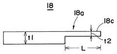
상기 칸막이판의 앞끝단부는, 도 4에 나타낸 바와 같이 두께가 연속적으로 얇아지도록 테이퍼형상으로 형성되어 있다. 그리고, 상기 칸막이판(18,19)은 같은 형상이기 때문에, 간만기판(18)에 대하여 설명한다.As shown in Fig. 4, the front end of the partition plate is formed in a tapered shape so that the thickness is continuously thinned. Since the
상기 칸막이판(18)의 앞끝단부(18a)는, 칸막이판 자체의 두께(t1)에 따라 임의로 형성할 수 있다. 상기 앞끝단부(18a)의 테이퍼각(α)은, 칸막이판으로 구획된 각 유로의 가스유속 범위와 칸막이판의 강도, 가공성 등을 고려하면서 가능한한 작게 하는 것이 바람직하지만, 테이퍼각(α)을 너무 작게 하면 테이퍼면(18b)이 길어지고 강도와 가공성에 문제가 발생하는 일이 있다. 또, 테이퍼각(α)을 크게 하면 앞끝단부(18a)의 두께를 연속적으로 얇게 한 효과가 작아진다. 통상의 사용범위에서의 바람직한 테이퍼각(α)은 5∼30도이며, 특히, 10도 이하로 하는 것이 효과적이다. 더구나, 테이퍼면(18b)은, 통상은 평면으로 형성되지만, 곡면(볼록면과 오목면)으로 해도 좋고, 평면과 각종 곡면을 복합시켜도 좋다. 또한, 앞끝단은 반드시 날카롭게 할 필요는 없고, 둥글게 하거나 끊어 놓은 형상으로 해도 좋다.The front end 18a of the
이와 같이 칸막이판의 앞끝단부의 두께를 얇게 형성함으로써, 칸막이판의 앞끝단부 근방에서의 가스 흐름의 혼란을 억제할 수 있고, 막의 균일성과 재현성이 향상된다. 또, 소용돌이에 기인하는 파티클의 발생도 감소하므로, 파티클이 원인으로 되는 결정결함도 감소하여 품질향상이 도모됨과 동시에, 원료이용효율의 향상도 도모된다. 게다가, 칸막이판에서 구획된 각 유로의 가스속도의 설정범위를 넓힐 수 있으므로, 박막성장에 최적인 가스유속을 설정할 수 있고, 성장속도의 향상도 도모할 수 있다.Thus, by forming the thickness of the front end of a partition board thin, the confusion of the gas flow in the vicinity of the front end of a partition board can be suppressed, and the uniformity and reproducibility of a film improve. In addition, since the generation of particles due to vortices is reduced, crystal defects caused by particles are also reduced, thereby improving quality and improving raw material utilization efficiency. In addition, since the setting range of the gas velocity of each flow path partitioned in the partition plate can be widened, the gas flow rate that is optimal for thin film growth can be set, and the growth rate can be improved.
도 5∼9는, 각각 칸막이판의 앞끝단부의 다른 형태예를 나타낸 것이다.5-9 show another example of the front end of a partition plate, respectively.
도 5에 나타낸 칸막이판(18)은, 앞끝단부(18a)의 상하 양면에 테이퍼면(18b)을 각각 형성한 것이다. 테이퍼각(α)은, 상기와 마찬가지로, 5∼30도, 특히 10도 이하로 설정하는 것이 바람직하다.The
도 6에 나타낸 칸막이판(18)은, 앞끝단부(18a)의 두께를 단계적으로 얇아지도록 형성한 것이다. 이 칸막이판(18)은, 칸막이판 자체의 두께(t1)보다 앞끝단부(18a)의 두께(t2)를 충분히 얇게 하고, 얇은 두께부(18c)의 길이(L)를 충분히 취하도록 하고 있다. 이 얇은 두께부(18c)의 두께(t2) 및 길이(L)는, 상기 테이퍼각(α)과 마찬가지로, 칸막이판 자체의 두께(t1)와 가스유속, 칸막이판의 강도, 가공성 등을 고려하여 결정되지만, 두께(t2)는 얇을수록 효과적이고, 길이(L)도 길수록 효과적이다. 바람직한 범위는, 두께(t2)는 0.5∼1mm, 길이(L)는 단차(t1-t2)가 큰 경우에는 약간 길게 하는 것이 바람직하고, 통상은 10∼20mm정도이다.The
도 7에 나타낸 칸막이판(18)은, 앞끝단부(18a)를 2단계로 얇은 두께부(18c,18d)로 형성하여, 두께를 단계적으로 얇게 하고 있다. 그리고, 앞끝단부(18a)는 3단계 이상으로 형성해도 좋다.The
도 8에 나타낸 칸막이판(18)은, 앞끝단부(18a)의 상하 양측에 단부(18e)를 각각 설치하여 단계적으로 얇은 두께로 형성한 것이다. 도 9에 나타낸 칸막이판(18)은, 앞끝단부(18a)의 상하 양측에 단부(18e,18f)를 2단계 설치하여 얇은 두께로 형성한 것이다.In the
또한, 앞끝단부(18a)의 두께를 상술한 바와 같이 단계적으로 얇게 형성하는 경우, 단부를 테이퍼면으로 하는 것도 가능하고, 얇은 두께부의 앞끝단을 둥글게 하거나 날카롭게 하는 것도 가능하다. 그리고, 도 4, 도 6 및 도 7에 나타낸 칸막이판은, 상하를 역으로 해도 좋고, 도 5, 도 8 및 도 9에 나타낸 칸막이판은 상하를 비대칭으로 형성해도 좋다.In addition, when forming the thickness of the front end part 18a thinly step by step as mentioned above, it is also possible to make an end into a taper surface, and it is also possible to round or sharpen the front end of a thin thickness part. The partition plates shown in Figs. 4, 6 and 7 may be reversed up and down, and the partition plates shown in Figs. 5, 8 and 9 may be formed asymmetrically up and down.
그리고, 상기 칸막이판(18,19)에는, 같은 형상인 것을 이용하는 것이 바람직하지만, 다른 형상인 것을 조합할 수도 있다.In addition, although it is preferable to use the thing of the same shape for the said
[실험예 1]Experimental Example 1
도 1, 도 2에 나타낸 구조의 장치를 이용하여, GaAs 기판상에 GaAs막을 성막하는 실험을 하기의 조건으로 행하였다. 제 1 유로에는, 휘발성 원료가스인 아르신과 도핑가스인 실란을 수소로 희석한 가스를 도입하고, 제 2 유로에는, 난휘발성가스인 트리메틸갈륨(TMG)을 수소로 희석한 가스를 도입하고, 제 3 유로에는, 성장촉진가스로서 수소를 도입하였다. 그리고, 도핑가스인 실란의 농도는 10ppm으로 하였다.Experiments for forming a GaAs film on a GaAs substrate using the apparatus of the structure shown in Figs. 1 and 2 were carried out under the following conditions. A gas obtained by diluting arsine, which is a volatile raw material gas, and a silane, which is a doping gas, with hydrogen is introduced into the first flow path, and a gas obtained by diluting trimethylgallium (TMG), which is a nonvolatile gas, with hydrogen is introduced into the second flow path. Hydrogen was introduced into the three flow paths as the growth promoting gas. And the concentration of silane which is a doping gas was 10 ppm.
도 3은, 3인치 GaAs 기판상에 GaAs를 성막했을 때의 희석가스유량 밸런스와 기판면에의 막두께 균일성 및 Si 도핑균일성과의 관계를 나타낸 것으로, 가로축이 희석가스유량 밸런스[-], 세로축이 막두께 균일성[%] 및 Si 도핑균일성[%]을 나타내고 있다. 그리고, 막두께는 분광엘립소메트리로, Si 도핑양은 프로파일플롯터로 캐리어농도를 측정한 결과이다.Fig. 3 shows the relationship between the dilution gas flow rate balance when GaAs is deposited on a 3-inch GaAs substrate, the film thickness uniformity on the substrate surface, and the Si doping uniformity, and the horizontal axis shows the dilution gas flow rate balance [-], The vertical axis shows film thickness uniformity [%] and Si doping uniformity [%]. The film thickness is the spectroscopic ellipsometry and the Si doping amount is the result of measuring the carrier concentration with a profile plotter.
이 결과에서, 희석가스의 유량 밸런스를 크게 하는, 다시 말해 제 1 유로의 제 1 기상성장가스중의 희석가스유량을 증대시킴에 따라 막두께 균일성이 작아지고, 어떤 점을 경계로 두께 균일성이 다시 커지는 것을 알 수 있다. 또한, 도핑 균일성에 대해서는, 두께 균일성이 얻어지는 최적인 희석가스유량 밸런스 조건과 일치하고 있음을 알 수 있다. 이것으로부터, 표 1에 나타낸 조건으로 성막을 행한 바, 균일하고 양호한 GaAs막을 얻을 수 있었다.As a result, the film thickness uniformity decreases as the dilution gas flow rate balance is increased, that is, the dilution gas flow rate in the first gaseous phase growth gas of the first flow path is increased. You can see this grows again. In addition, it can be seen that the doping uniformity coincides with the optimum dilution gas flow rate balance condition to obtain the thickness uniformity. From this, when the film was formed under the conditions shown in Table 1, a uniform and favorable GaAs film was obtained.
표 1Table 1
그리고, 희석가스 유량 밸런스는, 8000sccm/12000sccm=0.67sccm이다. 또한 sccm은, 〔Standard Cubic Centimeter/min〕의 약자이다.The dilution gas flow rate balance is 8000sccm / 12000sccm = 0.67sccm. In addition, sccm is an abbreviation of [Standard Cubic Centimeter / min].
[실험예 2]Experimental Example 2
앞끝단부의 두께를 연속적으로 테이퍼형상으로 얇게 한 도 4에 나타낸 형상의 칸막이판(t1=1.5mm)에 있어서, 테이퍼각(α)이 5도, 10도, 20도, 30도, 60도, 90도(테이퍼면 없음)인 6종류의 칸막이판을 각 2매씩 사용하고, 도 1 및 도2에 나타낸 바와 같이 배설하여 반응관내의 상류쪽에 제 1 유로, 제 2 유로, 제 3 유로의 3층 유로를 형성하였다. 이 반응관을 이용하여 하기의 성장조건에 따라, AlN을 미리 형성한 사파이어기판상에 GaN박막을 각각 성장시켰다. 얻어진 박막 표면을 미분간섭 현미경으로 관찰한 바, 테이퍼면이 없는 칸막이판을 사용했을 때에는, 발생한 파티클이 핵으로 되어 성장한 부분이 있기 때문에 거칠게 되어 있고, 막 두께가 불균일하게 되어 있었지만, 테이퍼각(α)이 작아짐에 반하여 표면이 평탄하게 되고, 특히 테이퍼각(α)이 20도 이하인 것은, 막표면의 평탄성에 뛰어나 있으며, 표면상태의 개선효과가 컸다. 각 칸막이판을 사용했을 때의 GaN박막의 성장속도 및 표면상태의 관찰결과를 표 2에 나타낸다.In the partition plate (t1 = 1.5 mm) of the shape shown in FIG. 4 in which the thickness of the front end portion was continuously thinned to the tapered shape, the taper angle α was 5 degrees, 10 degrees, 20 degrees, 30 degrees, 60 degrees, Six partition plates of 90 degrees (without tapered surface) are used, and each of them is disposed as shown in Figs. 1 and 2, and the three layers of the first flow passage, the second flow passage, and the third flow passage are disposed upstream in the reaction tube. A flow path was formed. By using this reaction tube, GaN thin films were grown on sapphire substrates on which AlN was formed in advance according to the following growth conditions. When the obtained thin film surface was observed with a microscopic microscope, when a partition plate without a tapered surface was used, the generated particles became a nucleus and grew to become rough, and the film thickness was uneven, but the taper angle (α ), The surface becomes flat while the taper angle α is 20 degrees or less, which is excellent in the flatness of the film surface, and has a great effect of improving the surface state. Table 2 shows the results of observation of the growth rate and surface state of the GaN thin film when each partition plate was used.
성장조건Growth conditions
제 1 유로 : 암모니아(분당 12리터)First flow path: ammonia (12 liters per minute)
제 2 유로 : 트리메틸갈륨(분당 40μmol) + 수소(분당 6리터)Second flow path: trimethylgallium (40 μmol per minute) + hydrogen (6 liters per minute)
제 3 유로 : 질소(분당 14리터)Third flow path: nitrogen (14 liters per minute)
기판가열온도 : 1050℃Substrate Heating Temperature: 1050 ℃
성장압력 : 1기압Growth pressure: 1 atmosphere
성장시간 : 1시간Growth time: 1 hour
표 2TABLE 2
[실험예 3]Experimental Example 3
앞끝단부의 두께를 단계적으로 얇게 한 도 6에 나타낸 형상의 칸막이판(t1=1.5mm, t2=0.5mm)에 있어서, 얇은 두께부의 길이(L)를 0mm(얇은 두께부 없음), 5mm, 10mm, 20mm로 한 4종류의 칸막이판을 사용하고, 실험예 2와 같이 반응관내에 3층의 유로를 형성하였다. 하기의 성장조건에 의해 실험예 2와 같은 GaN박막을 성장시킴에 있어, 원료가스인 암모니아의 유량을 분당 3리터, 5리터, 10리터, 15리터로 변화시켜, 얻어진 박막 표면을 미분간섭 현미경으로 관찰하였다. 각 칸막이판에서의 얇은 두께부의 길이(L)와 암모니아의 유량에서의 표면상태의 관찰결과를 표 3에 나타낸다.In the partition plate (t1 = 1.5mm, t2 = 0.5mm) of the shape shown in FIG. 6 in which the thickness of the front end was thinned step by step, the length L of the thin thickness portion was 0 mm (no thin thickness portion), 5 mm, 10 mm. 4 partition plates of 20 mm were used, and three flow paths were formed in the reaction tube as in Experimental Example 2. In growing the same GaN thin film as in Experimental Example 2 under the following growth conditions, the flow rate of ammonia as a raw material gas was changed to 3 liters, 5 liters, 10 liters, and 15 liters per minute. Observed. Table 3 shows the results of the observation of the surface state at the length L of the thin-thickness portion in each partition plate and the flow rate of ammonia.
성장조건Growth conditions
제 1 유로 : 암모니아(분당 3, 5, 10, 15리터)First flow path: ammonia (3, 5, 10, 15 liters per minute)
제 2 유로 : 트리메틸갈륨(분당 40μmol) + 수소(분당 8리터)Second flow path: trimethylgallium (40 μmol per minute) + hydrogen (8 liters per minute)
제 3 유로 : 질소(분당 14리터)Third flow path: nitrogen (14 liters per minute)
기판가열온도 : 1050℃Substrate Heating Temperature: 1050 ℃
성장압력 : 1기압Growth pressure: 1 atmosphere
성장시간 : 1시간Growth time: 1 hour
표 3TABLE 3
이상에서와 같이 본 발명의 기상성장장치 및 기상성장방법에 의하면, 이성분계 이상의 화합물 반도체박막을 효율 좋게 생산할 수 있고, 복잡한 다층구조의 디바이스용 박막의 최적화도 용이하게 된다. 또, 유해퇴적물의 감소에 의해 반응관의 청소빈도가 감소하여 생산성이 향상된다.As described above, according to the vapor phase growth apparatus and the vapor phase growth method of the present invention, compound semiconductor thin films of two or more components can be efficiently produced, and the optimization of thin films for devices having a complicated multilayer structure is also facilitated. Moreover, the frequency of cleaning of the reaction tube is reduced by the reduction of harmful deposits, and the productivity is improved.
또한, 상기 칸막이판의 앞끝단부를 두께가 연속적으로 얇아지도록 형성하든지, 혹은 두께가 단계적으로 얇아지도록 형성함으로써, 양질이며 균일성에 우수한 박막을 효율 좋게 제조할 수 있다. 특히, 기판을 설치한 반응관내에 적어도 2종류의 원료가스를 기판면에 대하여 평행한 방향으로 도입하고, 상기 기판면에 이성분계 이상의 화합물 반도체박막을 형성하는 기상성장장치에 최적이다.In addition, by forming the front end of the partition plate so that the thickness is continuously thin, or by forming the thickness is gradually thinned, it is possible to efficiently produce a thin film of good quality and excellent uniformity. In particular, at least two types of raw material gases are introduced into a reaction tube provided with a substrate in a direction parallel to the substrate surface, and are ideal for a vapor phase growth apparatus for forming a compound semiconductor thin film of two or more components on the substrate surface.
Claims (8)
Translated fromKoreanApplications Claiming Priority (5)
| Application Number | Priority Date | Filing Date | Title |
|---|---|---|---|
| JP66396 | 1996-03-22 | ||
| JP06639696AJP3880096B2 (en) | 1996-03-22 | 1996-03-22 | Vapor growth method |
| JP25505 | 1997-02-07 | ||
| JP02550597AJP3936425B2 (en) | 1997-02-07 | 1997-02-07 | Vapor growth method |
| PCT/JP1997/000867WO1997036320A1 (en) | 1996-03-22 | 1997-03-18 | Vapor phase growth apparatus and vapor phase growth method |
Publications (2)
| Publication Number | Publication Date |
|---|---|
| KR19990021855A KR19990021855A (en) | 1999-03-25 |
| KR100272752B1true KR100272752B1 (en) | 2001-05-02 |
Family
ID=26363126
Family Applications (1)
| Application Number | Title | Priority Date | Filing Date |
|---|---|---|---|
| KR1019970708329AExpired - Fee RelatedKR100272752B1 (en) | 1996-03-22 | 1997-03-18 | Vapor phase growth apparatus and vapor phase growth method |
Country Status (6)
| Country | Link |
|---|---|
| US (1) | US6190457B1 (en) |
| EP (2) | EP1220305B1 (en) |
| KR (1) | KR100272752B1 (en) |
| DE (1) | DE69732722T2 (en) |
| TW (1) | TW320754B (en) |
| WO (1) | WO1997036320A1 (en) |
Families Citing this family (114)
| Publication number | Priority date | Publication date | Assignee | Title |
|---|---|---|---|---|
| US6093252A (en)* | 1995-08-03 | 2000-07-25 | Asm America, Inc. | Process chamber with inner support |
| KR100271831B1 (en)* | 1998-01-17 | 2000-11-15 | 박근섭 | Horizontal reactor for compound semiconductor growth |
| US6544869B1 (en)* | 2000-06-23 | 2003-04-08 | Matsushita Electric Industrial Co., Ltd. | Method and apparatus for depositing semiconductor film and method for fabricating semiconductor device |
| TW544775B (en)* | 2001-02-28 | 2003-08-01 | Japan Pionics | Chemical vapor deposition apparatus and chemical vapor deposition method |
| JP2006080374A (en)* | 2004-09-10 | 2006-03-23 | Sharp Corp | Nitride semiconductor manufacturing apparatus and nitride semiconductor laser device |
| JP2008540840A (en)* | 2005-05-09 | 2008-11-20 | エイエスエム・ジェニテック・コリア・リミテッド | Reactor of atomic layer deposition apparatus with multiple gas inlets |
| JP4193883B2 (en) | 2006-07-05 | 2008-12-10 | 住友電気工業株式会社 | Metalorganic vapor phase epitaxy system |
| US20080241384A1 (en)* | 2007-04-02 | 2008-10-02 | Asm Genitech Korea Ltd. | Lateral flow deposition apparatus and method of depositing film by using the apparatus |
| US8282735B2 (en)* | 2007-11-27 | 2012-10-09 | Asm Genitech Korea Ltd. | Atomic layer deposition apparatus |
| US8628616B2 (en)* | 2007-12-11 | 2014-01-14 | Sumitomo Electric Industries, Ltd. | Vapor-phase process apparatus, vapor-phase process method, and substrate |
| JP5060324B2 (en)* | 2008-01-31 | 2012-10-31 | 株式会社日立国際電気 | Substrate processing apparatus, semiconductor device manufacturing method, and processing container |
| US9394608B2 (en)* | 2009-04-06 | 2016-07-19 | Asm America, Inc. | Semiconductor processing reactor and components thereof |
| US8802201B2 (en) | 2009-08-14 | 2014-08-12 | Asm America, Inc. | Systems and methods for thin-film deposition of metal oxides using excited nitrogen-oxygen species |
| US9312155B2 (en) | 2011-06-06 | 2016-04-12 | Asm Japan K.K. | High-throughput semiconductor-processing apparatus equipped with multiple dual-chamber modules |
| US10854498B2 (en) | 2011-07-15 | 2020-12-01 | Asm Ip Holding B.V. | Wafer-supporting device and method for producing same |
| US9017481B1 (en) | 2011-10-28 | 2015-04-28 | Asm America, Inc. | Process feed management for semiconductor substrate processing |
| MX374974B (en) | 2012-10-12 | 2025-03-06 | Vitro Vidrio Y Cristal S A De C V | A COATING WITH SOLAR CONTROL PROPERTIES FOR A SUBSTRATE AND, A METHOD AND SYSTEM FOR DEPOSITING SAID COATING ON THE SUBSTRATE. |
| US10714315B2 (en) | 2012-10-12 | 2020-07-14 | Asm Ip Holdings B.V. | Semiconductor reaction chamber showerhead |
| US10683571B2 (en) | 2014-02-25 | 2020-06-16 | Asm Ip Holding B.V. | Gas supply manifold and method of supplying gases to chamber using same |
| US10167557B2 (en) | 2014-03-18 | 2019-01-01 | Asm Ip Holding B.V. | Gas distribution system, reactor including the system, and methods of using the same |
| US11015245B2 (en) | 2014-03-19 | 2021-05-25 | Asm Ip Holding B.V. | Gas-phase reactor and system having exhaust plenum and components thereof |
| US10858737B2 (en) | 2014-07-28 | 2020-12-08 | Asm Ip Holding B.V. | Showerhead assembly and components thereof |
| US9890456B2 (en) | 2014-08-21 | 2018-02-13 | Asm Ip Holding B.V. | Method and system for in situ formation of gas-phase compounds |
| US10941490B2 (en) | 2014-10-07 | 2021-03-09 | Asm Ip Holding B.V. | Multiple temperature range susceptor, assembly, reactor and system including the susceptor, and methods of using the same |
| US9657845B2 (en) | 2014-10-07 | 2017-05-23 | Asm Ip Holding B.V. | Variable conductance gas distribution apparatus and method |
| US10600673B2 (en) | 2015-07-07 | 2020-03-24 | Asm Ip Holding B.V. | Magnetic susceptor to baseplate seal |
| US10211308B2 (en) | 2015-10-21 | 2019-02-19 | Asm Ip Holding B.V. | NbMC layers |
| US11139308B2 (en) | 2015-12-29 | 2021-10-05 | Asm Ip Holding B.V. | Atomic layer deposition of III-V compounds to form V-NAND devices |
| US10529554B2 (en) | 2016-02-19 | 2020-01-07 | Asm Ip Holding B.V. | Method for forming silicon nitride film selectively on sidewalls or flat surfaces of trenches |
| US10865475B2 (en) | 2016-04-21 | 2020-12-15 | Asm Ip Holding B.V. | Deposition of metal borides and silicides |
| US10032628B2 (en) | 2016-05-02 | 2018-07-24 | Asm Ip Holding B.V. | Source/drain performance through conformal solid state doping |
| US11453943B2 (en) | 2016-05-25 | 2022-09-27 | Asm Ip Holding B.V. | Method for forming carbon-containing silicon/metal oxide or nitride film by ALD using silicon precursor and hydrocarbon precursor |
| US10714385B2 (en) | 2016-07-19 | 2020-07-14 | Asm Ip Holding B.V. | Selective deposition of tungsten |
| KR102532607B1 (en) | 2016-07-28 | 2023-05-15 | 에이에스엠 아이피 홀딩 비.브이. | Substrate processing apparatus and method of operating the same |
| US10643826B2 (en) | 2016-10-26 | 2020-05-05 | Asm Ip Holdings B.V. | Methods for thermally calibrating reaction chambers |
| US11532757B2 (en) | 2016-10-27 | 2022-12-20 | Asm Ip Holding B.V. | Deposition of charge trapping layers |
| US10714350B2 (en) | 2016-11-01 | 2020-07-14 | ASM IP Holdings, B.V. | Methods for forming a transition metal niobium nitride film on a substrate by atomic layer deposition and related semiconductor device structures |
| US10643904B2 (en) | 2016-11-01 | 2020-05-05 | Asm Ip Holdings B.V. | Methods for forming a semiconductor device and related semiconductor device structures |
| TWI612176B (en)* | 2016-11-01 | 2018-01-21 | 漢民科技股份有限公司 | Gas distribution apparatus for deposition system |
| US10134757B2 (en) | 2016-11-07 | 2018-11-20 | Asm Ip Holding B.V. | Method of processing a substrate and a device manufactured by using the method |
| KR102546317B1 (en) | 2016-11-15 | 2023-06-21 | 에이에스엠 아이피 홀딩 비.브이. | Gas supply unit and substrate processing apparatus including the same |
| KR102762543B1 (en) | 2016-12-14 | 2025-02-05 | 에이에스엠 아이피 홀딩 비.브이. | Substrate processing apparatus |
| US11581186B2 (en) | 2016-12-15 | 2023-02-14 | Asm Ip Holding B.V. | Sequential infiltration synthesis apparatus |
| US11447861B2 (en) | 2016-12-15 | 2022-09-20 | Asm Ip Holding B.V. | Sequential infiltration synthesis apparatus and a method of forming a patterned structure |
| KR102700194B1 (en) | 2016-12-19 | 2024-08-28 | 에이에스엠 아이피 홀딩 비.브이. | Substrate processing apparatus |
| US10867788B2 (en) | 2016-12-28 | 2020-12-15 | Asm Ip Holding B.V. | Method of forming a structure on a substrate |
| US11390950B2 (en) | 2017-01-10 | 2022-07-19 | Asm Ip Holding B.V. | Reactor system and method to reduce residue buildup during a film deposition process |
| US10655221B2 (en) | 2017-02-09 | 2020-05-19 | Asm Ip Holding B.V. | Method for depositing oxide film by thermal ALD and PEALD |
| USD876504S1 (en) | 2017-04-03 | 2020-02-25 | Asm Ip Holding B.V. | Exhaust flow control ring for semiconductor deposition apparatus |
| KR102457289B1 (en) | 2017-04-25 | 2022-10-21 | 에이에스엠 아이피 홀딩 비.브이. | Method for depositing a thin film and manufacturing a semiconductor device |
| US10770286B2 (en) | 2017-05-08 | 2020-09-08 | Asm Ip Holdings B.V. | Methods for selectively forming a silicon nitride film on a substrate and related semiconductor device structures |
| US10892156B2 (en) | 2017-05-08 | 2021-01-12 | Asm Ip Holding B.V. | Methods for forming a silicon nitride film on a substrate and related semiconductor device structures |
| US12040200B2 (en) | 2017-06-20 | 2024-07-16 | Asm Ip Holding B.V. | Semiconductor processing apparatus and methods for calibrating a semiconductor processing apparatus |
| US11306395B2 (en) | 2017-06-28 | 2022-04-19 | Asm Ip Holding B.V. | Methods for depositing a transition metal nitride film on a substrate by atomic layer deposition and related deposition apparatus |
| US10685834B2 (en) | 2017-07-05 | 2020-06-16 | Asm Ip Holdings B.V. | Methods for forming a silicon germanium tin layer and related semiconductor device structures |
| KR20190009245A (en) | 2017-07-18 | 2019-01-28 | 에이에스엠 아이피 홀딩 비.브이. | Methods for forming a semiconductor device structure and related semiconductor device structures |
| US11018002B2 (en) | 2017-07-19 | 2021-05-25 | Asm Ip Holding B.V. | Method for selectively depositing a Group IV semiconductor and related semiconductor device structures |
| US11374112B2 (en) | 2017-07-19 | 2022-06-28 | Asm Ip Holding B.V. | Method for depositing a group IV semiconductor and related semiconductor device structures |
| US10590535B2 (en) | 2017-07-26 | 2020-03-17 | Asm Ip Holdings B.V. | Chemical treatment, deposition and/or infiltration apparatus and method for using the same |
| TWI815813B (en) | 2017-08-04 | 2023-09-21 | 荷蘭商Asm智慧財產控股公司 | Showerhead assembly for distributing a gas within a reaction chamber |
| US10692741B2 (en) | 2017-08-08 | 2020-06-23 | Asm Ip Holdings B.V. | Radiation shield |
| US10770336B2 (en) | 2017-08-08 | 2020-09-08 | Asm Ip Holding B.V. | Substrate lift mechanism and reactor including same |
| US10249524B2 (en) | 2017-08-09 | 2019-04-02 | Asm Ip Holding B.V. | Cassette holder assembly for a substrate cassette and holding member for use in such assembly |
| USD900036S1 (en) | 2017-08-24 | 2020-10-27 | Asm Ip Holding B.V. | Heater electrical connector and adapter |
| US11830730B2 (en) | 2017-08-29 | 2023-11-28 | Asm Ip Holding B.V. | Layer forming method and apparatus |
| KR102491945B1 (en) | 2017-08-30 | 2023-01-26 | 에이에스엠 아이피 홀딩 비.브이. | Substrate processing apparatus |
| US11056344B2 (en) | 2017-08-30 | 2021-07-06 | Asm Ip Holding B.V. | Layer forming method |
| US11295980B2 (en) | 2017-08-30 | 2022-04-05 | Asm Ip Holding B.V. | Methods for depositing a molybdenum metal film over a dielectric surface of a substrate by a cyclical deposition process and related semiconductor device structures |
| KR102401446B1 (en) | 2017-08-31 | 2022-05-24 | 에이에스엠 아이피 홀딩 비.브이. | Substrate processing apparatus |
| KR102630301B1 (en) | 2017-09-21 | 2024-01-29 | 에이에스엠 아이피 홀딩 비.브이. | Method of sequential infiltration synthesis treatment of infiltrateable material and structures and devices formed using same |
| US10844484B2 (en) | 2017-09-22 | 2020-11-24 | Asm Ip Holding B.V. | Apparatus for dispensing a vapor phase reactant to a reaction chamber and related methods |
| US10658205B2 (en) | 2017-09-28 | 2020-05-19 | Asm Ip Holdings B.V. | Chemical dispensing apparatus and methods for dispensing a chemical to a reaction chamber |
| US10923344B2 (en) | 2017-10-30 | 2021-02-16 | Asm Ip Holding B.V. | Methods for forming a semiconductor structure and related semiconductor structures |
| US10910262B2 (en) | 2017-11-16 | 2021-02-02 | Asm Ip Holding B.V. | Method of selectively depositing a capping layer structure on a semiconductor device structure |
| KR102443047B1 (en) | 2017-11-16 | 2022-09-14 | 에이에스엠 아이피 홀딩 비.브이. | Method of processing a substrate and a device manufactured by the same |
| US11022879B2 (en) | 2017-11-24 | 2021-06-01 | Asm Ip Holding B.V. | Method of forming an enhanced unexposed photoresist layer |
| TWI799494B (en) | 2018-01-19 | 2023-04-21 | 荷蘭商Asm 智慧財產控股公司 | Deposition method |
| USD903477S1 (en) | 2018-01-24 | 2020-12-01 | Asm Ip Holdings B.V. | Metal clamp |
| US11018047B2 (en) | 2018-01-25 | 2021-05-25 | Asm Ip Holding B.V. | Hybrid lift pin |
| US11081345B2 (en) | 2018-02-06 | 2021-08-03 | Asm Ip Holding B.V. | Method of post-deposition treatment for silicon oxide film |
| US10896820B2 (en) | 2018-02-14 | 2021-01-19 | Asm Ip Holding B.V. | Method for depositing a ruthenium-containing film on a substrate by a cyclical deposition process |
| US10731249B2 (en) | 2018-02-15 | 2020-08-04 | Asm Ip Holding B.V. | Method of forming a transition metal containing film on a substrate by a cyclical deposition process, a method for supplying a transition metal halide compound to a reaction chamber, and related vapor deposition apparatus |
| KR102636427B1 (en) | 2018-02-20 | 2024-02-13 | 에이에스엠 아이피 홀딩 비.브이. | Substrate processing method and apparatus |
| US10658181B2 (en) | 2018-02-20 | 2020-05-19 | Asm Ip Holding B.V. | Method of spacer-defined direct patterning in semiconductor fabrication |
| US11473195B2 (en) | 2018-03-01 | 2022-10-18 | Asm Ip Holding B.V. | Semiconductor processing apparatus and a method for processing a substrate |
| US11629406B2 (en) | 2018-03-09 | 2023-04-18 | Asm Ip Holding B.V. | Semiconductor processing apparatus comprising one or more pyrometers for measuring a temperature of a substrate during transfer of the substrate |
| US11114283B2 (en) | 2018-03-16 | 2021-09-07 | Asm Ip Holding B.V. | Reactor, system including the reactor, and methods of manufacturing and using same |
| US11230766B2 (en) | 2018-03-29 | 2022-01-25 | Asm Ip Holding B.V. | Substrate processing apparatus and method |
| US11088002B2 (en) | 2018-03-29 | 2021-08-10 | Asm Ip Holding B.V. | Substrate rack and a substrate processing system and method |
| US12272527B2 (en) | 2018-05-09 | 2025-04-08 | Asm Ip Holding B.V. | Apparatus for use with hydrogen radicals and method of using same |
| US11718913B2 (en) | 2018-06-04 | 2023-08-08 | Asm Ip Holding B.V. | Gas distribution system and reactor system including same |
| US11286562B2 (en) | 2018-06-08 | 2022-03-29 | Asm Ip Holding B.V. | Gas-phase chemical reactor and method of using same |
| US10797133B2 (en) | 2018-06-21 | 2020-10-06 | Asm Ip Holding B.V. | Method for depositing a phosphorus doped silicon arsenide film and related semiconductor device structures |
| US10612136B2 (en) | 2018-06-29 | 2020-04-07 | ASM IP Holding, B.V. | Temperature-controlled flange and reactor system including same |
| US10767789B2 (en) | 2018-07-16 | 2020-09-08 | Asm Ip Holding B.V. | Diaphragm valves, valve components, and methods for forming valve components |
| US11053591B2 (en) | 2018-08-06 | 2021-07-06 | Asm Ip Holding B.V. | Multi-port gas injection system and reactor system including same |
| US10883175B2 (en) | 2018-08-09 | 2021-01-05 | Asm Ip Holding B.V. | Vertical furnace for processing substrates and a liner for use therein |
| US10829852B2 (en) | 2018-08-16 | 2020-11-10 | Asm Ip Holding B.V. | Gas distribution device for a wafer processing apparatus |
| US11430674B2 (en) | 2018-08-22 | 2022-08-30 | Asm Ip Holding B.V. | Sensor array, apparatus for dispensing a vapor phase reactant to a reaction chamber and related methods |
| US11024523B2 (en) | 2018-09-11 | 2021-06-01 | Asm Ip Holding B.V. | Substrate processing apparatus and method |
| US11049751B2 (en) | 2018-09-14 | 2021-06-29 | Asm Ip Holding B.V. | Cassette supply system to store and handle cassettes and processing apparatus equipped therewith |
| US11232963B2 (en) | 2018-10-03 | 2022-01-25 | Asm Ip Holding B.V. | Substrate processing apparatus and method |
| US10847365B2 (en) | 2018-10-11 | 2020-11-24 | Asm Ip Holding B.V. | Method of forming conformal silicon carbide film by cyclic CVD |
| US10811256B2 (en) | 2018-10-16 | 2020-10-20 | Asm Ip Holding B.V. | Method for etching a carbon-containing feature |
| US12378665B2 (en) | 2018-10-26 | 2025-08-05 | Asm Ip Holding B.V. | High temperature coatings for a preclean and etch apparatus and related methods |
| US11087997B2 (en) | 2018-10-31 | 2021-08-10 | Asm Ip Holding B.V. | Substrate processing apparatus for processing substrates |
| US11031242B2 (en) | 2018-11-07 | 2021-06-08 | Asm Ip Holding B.V. | Methods for depositing a boron doped silicon germanium film |
| US10818758B2 (en) | 2018-11-16 | 2020-10-27 | Asm Ip Holding B.V. | Methods for forming a metal silicate film on a substrate in a reaction chamber and related semiconductor device structures |
| US10847366B2 (en) | 2018-11-16 | 2020-11-24 | Asm Ip Holding B.V. | Methods for depositing a transition metal chalcogenide film on a substrate by a cyclical deposition process |
| US10559458B1 (en) | 2018-11-26 | 2020-02-11 | Asm Ip Holding B.V. | Method of forming oxynitride film |
| US12040199B2 (en) | 2018-11-28 | 2024-07-16 | Asm Ip Holding B.V. | Substrate processing apparatus for processing substrates |
| US11217444B2 (en) | 2018-11-30 | 2022-01-04 | Asm Ip Holding B.V. | Method for forming an ultraviolet radiation responsive metal oxide-containing film |
| US11158513B2 (en) | 2018-12-13 | 2021-10-26 | Asm Ip Holding B.V. | Methods for forming a rhenium-containing film on a substrate by a cyclical deposition process and related semiconductor device structures |
| US11032945B2 (en)* | 2019-07-12 | 2021-06-08 | Applied Materials, Inc. | Heat shield assembly for an epitaxy chamber |
Citations (3)
| Publication number | Priority date | Publication date | Assignee | Title |
|---|---|---|---|---|
| JPH06163415A (en)* | 1992-11-18 | 1994-06-10 | Fujitsu Ltd | Vapor phase epitaxial growth system |
| JPH0778773A (en)* | 1993-09-07 | 1995-03-20 | Nissin Electric Co Ltd | Thin film vapor growth device |
| JPH08288224A (en)* | 1995-04-17 | 1996-11-01 | Furukawa Electric Co Ltd:The | Vapor phase growth equipment |
Family Cites Families (8)
| Publication number | Priority date | Publication date | Assignee | Title |
|---|---|---|---|---|
| JPH0727868B2 (en)* | 1987-04-22 | 1995-03-29 | 日本酸素株式会社 | Vapor phase growth equipment |
| US5087531A (en)* | 1988-11-30 | 1992-02-11 | Sharp Kabushiki Kaisha | Electroluminescent device |
| JP2881828B2 (en) | 1989-08-04 | 1999-04-12 | 富士通株式会社 | Vapor phase growth apparatus and vapor phase growth method |
| JP2768023B2 (en)* | 1991-01-31 | 1998-06-25 | 日本電気株式会社 | Vapor growth method |
| JP2850549B2 (en)* | 1991-01-31 | 1999-01-27 | 日本電気株式会社 | Vapor growth method |
| JP3131005B2 (en)* | 1992-03-06 | 2001-01-31 | パイオニア株式会社 | Compound semiconductor vapor deposition equipment |
| JPH0727868A (en) | 1993-07-13 | 1995-01-31 | N T T Facilities:Kk | Device for detecting position of buried metallic object |
| JP3181171B2 (en)* | 1994-05-20 | 2001-07-03 | シャープ株式会社 | Vapor phase growth apparatus and vapor phase growth method |
- 1997
- 1997-03-18KRKR1019970708329Apatent/KR100272752B1/ennot_activeExpired - Fee Related
- 1997-03-18WOPCT/JP1997/000867patent/WO1997036320A1/ennot_activeCeased
- 1997-03-18EPEP02004974Apatent/EP1220305B1/ennot_activeExpired - Lifetime
- 1997-03-18DEDE69732722Tpatent/DE69732722T2/ennot_activeExpired - Lifetime
- 1997-03-18EPEP97907358Apatent/EP0837495B1/ennot_activeExpired - Lifetime
- 1997-03-18USUS08/952,517patent/US6190457B1/ennot_activeExpired - Lifetime
- 1997-03-20TWTW086103492Apatent/TW320754B/zhactive
Patent Citations (3)
| Publication number | Priority date | Publication date | Assignee | Title |
|---|---|---|---|---|
| JPH06163415A (en)* | 1992-11-18 | 1994-06-10 | Fujitsu Ltd | Vapor phase epitaxial growth system |
| JPH0778773A (en)* | 1993-09-07 | 1995-03-20 | Nissin Electric Co Ltd | Thin film vapor growth device |
| JPH08288224A (en)* | 1995-04-17 | 1996-11-01 | Furukawa Electric Co Ltd:The | Vapor phase growth equipment |
Also Published As
| Publication number | Publication date |
|---|---|
| EP1220305A1 (en) | 2002-07-03 |
| US6190457B1 (en) | 2001-02-20 |
| EP0837495A4 (en) | 2001-05-30 |
| EP0837495B1 (en) | 2003-05-14 |
| TW320754B (en) | 1997-11-21 |
| EP1220305B1 (en) | 2005-03-09 |
| EP0837495A1 (en) | 1998-04-22 |
| KR19990021855A (en) | 1999-03-25 |
| DE69732722D1 (en) | 2005-04-14 |
| DE69732722T2 (en) | 2006-02-02 |
| WO1997036320A1 (en) | 1997-10-02 |
Similar Documents
| Publication | Publication Date | Title |
|---|---|---|
| KR100272752B1 (en) | Vapor phase growth apparatus and vapor phase growth method | |
| EP0502209B1 (en) | Method and apparatus for growing compound semiconductor crystals | |
| JP3231996B2 (en) | Vapor phase growth equipment | |
| US9644267B2 (en) | Multi-gas straight channel showerhead | |
| US20090095221A1 (en) | Multi-gas concentric injection showerhead | |
| EP1271607A2 (en) | Chemical vapor deposition apparatus and method | |
| US20070045662A1 (en) | Substrate for film growth of group iii nitrides, method of manufacturing the same, and semiconductor device using the same | |
| US11879171B2 (en) | Semiconductor manufacturing device | |
| US20140109831A1 (en) | Vapor deposition method and vapor deposition apparatus | |
| US20150000596A1 (en) | Mocvd gas diffusion system with gas inlet baffles | |
| CN104141116A (en) | Metal organic chemical vapor deposition device, gas spray component and gas distribution control method | |
| US6184049B1 (en) | Method for fabricating compound semiconductor epitaxial wafer and vapor phase growth apparatus using the same | |
| US20010021593A1 (en) | Chemical vapor deposition apparatus and chemical vapor deposition process | |
| JP2007335800A (en) | Method and apparatus for manufacturing semiconductor thin film | |
| JP3880096B2 (en) | Vapor growth method | |
| JPH0677136A (en) | Method and device for vapor growing compound semiconductor thin film crystal | |
| JP2001284269A (en) | Vapor phase growth apparatus and method | |
| US20130295283A1 (en) | Chemical vapor deposition apparatus with multiple inlets for controlling film thickness and uniformity | |
| JPH11102871A (en) | Manufacture of semiconductor single-crystal thin film | |
| US20240183036A1 (en) | Epitaxial growth apparatus and multi-layer gas supply module used therefor | |
| WO2023063310A1 (en) | Method and apparatus for producing nitrogen compound | |
| JPH04338636A (en) | Semiconductor vapor phase growth equipment | |
| KR20030071098A (en) | Apparatus for manufacturing GaN substrate | |
| JPH06244109A (en) | Vapor growth method of compound semiconductor | |
| GB2404667A (en) | System for manufacturing III-V group compound semiconductors |
Legal Events
| Date | Code | Title | Description |
|---|---|---|---|
| PA0105 | International application | St.27 status event code:A-0-1-A10-A15-nap-PA0105 | |
| R17-X000 | Change to representative recorded | St.27 status event code:A-3-3-R10-R17-oth-X000 | |
| A201 | Request for examination | ||
| PA0201 | Request for examination | St.27 status event code:A-1-2-D10-D11-exm-PA0201 | |
| PG1501 | Laying open of application | St.27 status event code:A-1-1-Q10-Q12-nap-PG1501 | |
| E902 | Notification of reason for refusal | ||
| PE0902 | Notice of grounds for rejection | St.27 status event code:A-1-2-D10-D21-exm-PE0902 | |
| P11-X000 | Amendment of application requested | St.27 status event code:A-2-2-P10-P11-nap-X000 | |
| P13-X000 | Application amended | St.27 status event code:A-2-2-P10-P13-nap-X000 | |
| E701 | Decision to grant or registration of patent right | ||
| PE0701 | Decision of registration | St.27 status event code:A-1-2-D10-D22-exm-PE0701 | |
| GRNT | Written decision to grant | ||
| PR0701 | Registration of establishment | St.27 status event code:A-2-4-F10-F11-exm-PR0701 | |
| PR1002 | Payment of registration fee | St.27 status event code:A-2-2-U10-U12-oth-PR1002 Fee payment year number:1 | |
| PG1601 | Publication of registration | St.27 status event code:A-4-4-Q10-Q13-nap-PG1601 | |
| PR1001 | Payment of annual fee | St.27 status event code:A-4-4-U10-U11-oth-PR1001 Fee payment year number:4 | |
| PR1001 | Payment of annual fee | St.27 status event code:A-4-4-U10-U11-oth-PR1001 Fee payment year number:5 | |
| R18-X000 | Changes to party contact information recorded | St.27 status event code:A-5-5-R10-R18-oth-X000 | |
| PR1001 | Payment of annual fee | St.27 status event code:A-4-4-U10-U11-oth-PR1001 Fee payment year number:6 | |
| PR1001 | Payment of annual fee | St.27 status event code:A-4-4-U10-U11-oth-PR1001 Fee payment year number:7 | |
| PR1001 | Payment of annual fee | St.27 status event code:A-4-4-U10-U11-oth-PR1001 Fee payment year number:8 | |
| PR1001 | Payment of annual fee | St.27 status event code:A-4-4-U10-U11-oth-PR1001 Fee payment year number:9 | |
| FPAY | Annual fee payment | Payment date:20090508 Year of fee payment:10 | |
| PR1001 | Payment of annual fee | St.27 status event code:A-4-4-U10-U11-oth-PR1001 Fee payment year number:10 | |
| LAPS | Lapse due to unpaid annual fee | ||
| PC1903 | Unpaid annual fee | St.27 status event code:A-4-4-U10-U13-oth-PC1903 Not in force date:20100830 Payment event data comment text:Termination Category : DEFAULT_OF_REGISTRATION_FEE | |
| PC1903 | Unpaid annual fee | St.27 status event code:N-4-6-H10-H13-oth-PC1903 Ip right cessation event data comment text:Termination Category : DEFAULT_OF_REGISTRATION_FEE Not in force date:20100830 | |
| P22-X000 | Classification modified | St.27 status event code:A-4-4-P10-P22-nap-X000 |