KR100269643B1 - Power reduction circuit - Google Patents
Power reduction circuitDownload PDFInfo
- Publication number
- KR100269643B1 KR100269643B1KR1019970063285AKR19970063285AKR100269643B1KR 100269643 B1KR100269643 B1KR 100269643B1KR 1019970063285 AKR1019970063285 AKR 1019970063285AKR 19970063285 AKR19970063285 AKR 19970063285AKR 100269643 B1KR100269643 B1KR 100269643B1
- Authority
- KR
- South Korea
- Prior art keywords
- voltage
- operating voltage
- terminal
- mode
- power consumption
- Prior art date
- Legal status (The legal status is an assumption and is not a legal conclusion. Google has not performed a legal analysis and makes no representation as to the accuracy of the status listed.)
- Expired - Fee Related
Links
Images


Classifications
- G—PHYSICS
- G11—INFORMATION STORAGE
- G11C—STATIC STORES
- G11C5/00—Details of stores covered by group G11C11/00
- G11C5/14—Power supply arrangements, e.g. power down, chip selection or deselection, layout of wirings or power grids, or multiple supply levels
- G—PHYSICS
- G11—INFORMATION STORAGE
- G11C—STATIC STORES
- G11C5/00—Details of stores covered by group G11C11/00
- G11C5/14—Power supply arrangements, e.g. power down, chip selection or deselection, layout of wirings or power grids, or multiple supply levels
- G11C5/147—Voltage reference generators, voltage or current regulators; Internally lowered supply levels; Compensation for voltage drops
Landscapes
- Engineering & Computer Science (AREA)
- Power Engineering (AREA)
- Logic Circuits (AREA)
- Semiconductor Integrated Circuits (AREA)
- Power Sources (AREA)
- Dram (AREA)
Abstract
Description
Translated fromKorean본 발명은 전력소비 억제회로에 관한 것으로, 동작모드에 따라 공급전압의 크기를 변화시켜서 불필요한 전력소비를 억제하도록 하는 전력소비 억제회로에 관한 것이다. 특히 동작모드를 활성화 모드와 스탠바이 모드, 슬립 모드로 구분하고 각 모드에 따라 공급전압의 크기를 차별화 함으로써, 각 모드에 따른 양호한 전력소비 억제력과 스탠바이 모드에서 활성화 모드로 전환할 때의 빠른 동작속도를 모두 만족시킬 수 있도록 한 전력소비 억제회로에 관한 것이다.BACKGROUND OF THE
일반적으로 반도체 집적회로 등에서는 외부로부터의 조작 또는 조작에 따른 제어신호가 발생하는지를 판단하여 그 상태에 따라 공급전압의 크기를 제어함으로써 불필요한 전력소비를 억제한다. 즉, 외부로부터 일정시간 동안 제어신호가 입력되지 않게되면 이를 검출하여 회로를 스탠바이 모드(standby mode)로 전환하고, 공급전압을 다소 낮추어 공급한다. 이와 같은 스탠바이 모드의 상태에서 외부로부터 제어신호의 발생이 검출되면 정상적인 레벨의 전압을 공급함으로써 회로를 정상적으로 동작시키는 것이다.In general, semiconductor integrated circuits or the like determine whether a control signal according to an operation or an operation from the outside is generated and control the magnitude of the supply voltage according to the state to suppress unnecessary power consumption. That is, when the control signal is not input from the outside for a predetermined time, it detects this, switches the circuit to the standby mode, and supplies the voltage slightly lowered. When the generation of the control signal is detected from the outside in the standby mode, the circuit is normally operated by supplying a voltage of a normal level.
이와 같이 일반적인 활성화 모드와 스탠바이 모드에 따라 공급 전압의 크기를 적절하게 제어하는 종래의 전력소비 억제회로를 도 1에 나타내었다.As shown in FIG. 1, a conventional power consumption suppression circuit that appropriately controls the magnitude of the supply voltage in accordance with the general activation mode and the standby mode.
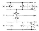
도 1에 나타낸 바와 같이, 전원전압(VDD) 단자와 접지전압(VSS) 단자에 저항(R1)(R2)이 각각 연결되는데, 이 저항(R1)(R2)을 통하여 국부전원전압(VDD_L)과 국부접지전압(VSS_L)을 각각 발생시킨다. 스위칭 소자인 피모스 트랜지스터(Q1)와 엔모스 트랜지스터(Q4)가 각각 저항(R1)(R2)과 병렬로 연결된다. 피모스 트랜지스터(Q1)는 반전된 활성화신호(/ACT)에 의해 제어되는데, 반전된 활성화신호(/ACT)가 로우 레벨일 때 턴 온되어 전원전압(VDD) 단자와 국부전원전압(VDD_L) 단자를 단락시킨다. 엔모스 트랜지스터(Q4)는 활성화신호(ACT)에 의해 제어되는데, 활성화신호(ACT)가 하이 레벨일 때 턴 온되어 접지전압(VSS) 단자와 국부접지전압(VSS_L) 단자를 단락시킨다.As shown in FIG. 1, resistors R1 and R2 are respectively connected to a power supply voltage VDD terminal and a ground voltage VSS terminal, and the local power supply voltage V is connected through the resistors R1 and R2.DD_L ) and the local ground voltage VSS_L . The switching element PMOS transistor Q1 and the NMOS transistor Q4 are connected in parallel with the resistors R1 and R2, respectively. The PMOS transistor Q1 is controlled by the inverted activation signal / ACT, which is turned on when the inverted activation signal / ACT is at a low level so that the power supply voltage VDD terminal and the local power supply voltage VDD_L ) Short the terminal. The NMOS transistor Q4 is controlled by the activation signal ACT. When the activation signal ACT is at a high level, the NMOS transistor Q4 shorts the ground voltage VSS terminal and the local ground voltage VSS_L terminal.
국부전원전압(VDD_L) 단자와 국부접지전압(VSS_L) 단자 사이에는 피모스 트랜지스터(Q2)와 엔모스 트랜지스터(Q3)로 구성된 시모스 인버터가 연결되어 있다. 이 시모스 인버터를 구성하는 피모스 트랜지스터(Q2)와 엔모스 트랜지스터(Q3)는 고속동작을 구현하기 위하여 다른 모스 트랜지스터보다 상대적으로 낮은 임계전압(threshold voltage, Vt)을 갖도록 설계된다.A CMOS inverter consisting of a PMOS transistor Q2 and an NMOS transistor Q3 is connected between the local power supply voltage VDD_L terminal and the local ground voltage VSS_L terminal. PMOS transistors Q2 and NMOS transistors Q3 constituting the CMOS inverter are designed to have a relatively lower threshold voltage (Vt ) than other MOS transistors in order to realize high-speed operation.
도 1에 나타낸 것과 같은 종래의 전력소비 억제회로는 실제로 도 2의 회로도와 같이 구현되는 것이 일반적이다. 도 2는 도 1에 나타낸 종래의 전력소비 억제회로에서 전압강하 수단을 모스 트랜지스터로 구현한 전력소비 억제회로이다.Conventional power consumption suppression circuits such as those shown in FIG. 1 are generally implemented as in the circuit diagram of FIG. 2. FIG. 2 is a power consumption suppression circuit in which the voltage drop means is implemented as a MOS transistor in the conventional power consumption suppression circuit shown in FIG.
도 2에 나타낸 전력소비 억제회로가 도 1과 다른 점은 전압강하 수단을 모스 트랜지스터로 구현한 것이다. 즉, 전원전압(VDD) 단자와 접지전압(VSS) 단자에 엔모스 트랜지스터(Q5)와 피모스 트랜지스터(Q6)를 연결하고, 게이트와 소스를 단락시켜서 각각 소정의 저항값을 갖는 저항소자로서 동작하도록 한 것이다.The power consumption suppression circuit shown in FIG. 2 is different from that in FIG. That is, the NMOS transistor Q5 and the PMOS transistor Q6 are connected to the power supply voltage (VDD ) terminal and the ground voltage (VSS ) terminal, and a resistance element having a predetermined resistance value by shorting the gate and the source, respectively. It is intended to operate as.
전원전압(VDD)과 국부전원전압(VDD_L)은 저항소자인 엔모스 트랜지스터(Q5)의 임계전압(Vtn) 만큼의 전압차를 갖는다. 즉 VDD_L=VDD-Vtn이 되는 것이다. 접지전압(VSS)과 국부접지전압(VSS_L) 역시 저항소자인 피모스 트랜지스터(Q6)의 임계전압(Vtp) 만큼의 전압차를 갖는다. 즉 VSS_L=VSS+Vtp가 된다.The power supply voltage VDD and the local power supply voltage VDD_L have a voltage difference equal to the threshold voltage Vtn of the NMOS transistor Q5 which is a resistance element. That is, VDD_L = VDD -Vtn . The ground voltage VSS and the local ground voltage VSS_L also have a voltage difference equal to the threshold voltage Vtp of the PMOS transistor Q6, which is a resistor. That is, VSS_L = VSS + Vtp .
활성화 모드에서는 활성화신호(ACT)가 하이 레벨로 되고 반전된 활성화신호(/ACT)는 로우 레벨로 되어 스위칭 소자인 피모스 트랜지스터(Q1)를 턴 온시킨다. 따라서 이때의 국부접지전압(VSS_L)은 전원전압(VDD)과 같아진다(단, 피모스 트랜지스터 Q1의 임계전압 Vtp에 따른 전압강하를 고려하지 않을 때). 또한 하이 레벨의 활성화신호(ACT)에 의해 엔모스 트랜지스터(Q4) 역시 턴 온되어 국부접지전압(VSS_L)은 접지전압(VSS)과 같아진다(엔모스 트랜지스터 Q4의 임계전압 Vtn에 따른 전압강하를 고려하지 않을 때). 따라서 활성화신호(ACT)가 하이 레벨로 되면 저항소자인 엔모스 트랜지스터(Q5)와 피모스 트랜지스터(Q6)는 국부전원전압(VDD_L)과 국부접지전압(VSS_L)의 변화에 아무런 영향도 미치지 못한다. 이 상태에서 시모스 인버터는 입력신호(IN)의 논리값에 따라 전원전압(VDD) 또는 접지전압(VSS) 레벨의 출력신호(OUT)를 발생시키는 것이다.In the activation mode, the activation signal ACT goes high and the inverted activation signal / ACT goes low to turn on the PMOS transistor Q1, which is a switching element. Therefore, the local ground voltage VSS_L at this time is equal to the power supply voltage VDD (when the voltage drop according to the threshold voltage Vtp of the PMOS transistor Q1 is not taken into account). The NMOS transistor Q4 is also turned on by the high level activation signal ACT so that the local ground voltage VSS_L is equal to the ground voltage VSS (according to the threshold voltage Vtn of the NMOS transistor Q4). Without considering the voltage drop). Therefore, when the activation signal ACT becomes high, the resistance elements NMOS transistor Q5 and PMOS transistor Q6 have no influence on the change of the local power supply voltage VDD_L and the local ground voltage VSS_L. In this state, the CMOS inverter generates an output signal OUT having a power supply voltage VDD or a ground voltage VSS according to the logic value of the input signal IN.
스탠바이 모드에서는 활성화신호(ACT)가 로우 레벨로 되고 반전된 활성화신호(/ACT)는 하이 레벨이 된다. 이 두 신호는 스위칭 소자인 피모스 트랜지스터(Q1)와 엔모스 트랜지스터(Q4)를 각각 턴 오프시킨다. 따라서 전원전압(VDD) 단자와 국부전원전압(VDD_L) 단자 사이에는 단지 저항소자인 엔모스 트랜지스터(Q5)에 의해 전류 경로가 형성되고, 접지전압(VSS) 단자와 국부접지전압(VSS_L) 단자 사이에도 단지 저항소자인 피모스 트랜지스터(Q6)에 의한 전류 경로가 형성된다. 이와같은 스탠바이 모드에서 시모스 인버터는 입력신호(IN)의 논리값에 따라 국부전원전압(VDD_L) 또는 국부접지전압(VSS_L) 레벨의 출력신호(OUT)를 발생시킨 것이다.In the standby mode, the activation signal ACT goes low and the inverted activation signal / ACT goes high. These two signals turn off the switching element PMOS transistor Q1 and NMOS transistor Q4, respectively. Therefore, a current path is formed between the power supply voltage (VDD ) terminal and the local power supply voltage (VDD_L ) terminal only by the NMOS transistor Q5, which is a resistance element, and the ground voltage (VSS ) terminal and the local ground voltage (V).Between the terminalsSS_L , a current path is formed by the PMOS transistor Q6 which is only a resistance element. The CMOS inverters on the same stand-by mode is that caused the local power source voltage (VDD_L) or the output signal (OUT) to the local ground voltage (VSS_L) level according to the logic value of the input signal (IN).
이와 같은 종래의 전력소비 억제회로에서, 저항소자인 엔모스 트랜지스터(Q5)와 피모스 트랜지스터(Q6)의 임계전압(Vtn)(Vtp)은 목적하는 전력소비 억제력을 고려하여 결정된다. 만약 전력소비 억제력을 높이기 위해서는 임계전압(Vtn)(Vtp)을 크게 형성하여 국부전원전압(VDD_L)을 크게 낮추면 된다. 그러나 임계전압(Vtn)(Vtp)의 크기를 너무 크게 형성하면 스탠바이 모드에서 활성화모드로 전환하는데 소요되는 시간이 매우 길어진다.In such a conventional power consumption suppression circuit, the threshold voltages Vtn (Vtp ) of the NMOS transistors Q5 and PMOS transistors Q6 which are resistance elements are determined in consideration of the desired power consumption suppression force. In order to increase the power consumption suppression power, the threshold voltage Vtn (Vtp ) may be large toreduce the local power supply voltage VDD_L . However, if the threshold voltage Vtn (Vtp ) is made too large, the time required for switching from the standby mode to the active mode becomes very long.
따라서 저항소자를 구현하기 위한 엔모스 트랜지스터(Q5)와 피모스 트랜지스터(Q6)의 임계전압(Vtn)(Vtp)을 충분히 크게 형성하지 못하게 되어 매우 양호한 전력소비 억제력은 기대할 수 없다. 만약 전력소비 억제력만을 고려하여 임계전압(Vtn)(Vtp)을 크게 형성하면 스탠바이 모드에서 활성화모드로 전환하는데 매우 오랜 시간이 소요되기 때문에 이때에는 빠른 동작속도를 기대할 수 없다. 그렇기 때문에 양호한 전력소비 억제력과 양호한 동작속도 가운데 하나를 선택하여 그에 부합하는 임계전압(Vtn)(Vtp)을 설정하는 수밖에 없다.Therefore, the threshold voltage Vtn (Vtp ) of the NMOS transistor Q5 and the PMOS transistor Q6 for implementing the resistance element may not be sufficiently large, and thus a very good power consumption suppression force cannot be expected. If the critical voltage (Vtn ) (Vtp ) is formed large in consideration of the power consumption restraint only, a very long time is required to switch from the standby mode to the active mode. Therefore, there is no choice but to set a threshold voltage (Vtn) Vtp corresponding to one of good power consumption suppression force and good operating speed.
따라서 본 발명은 회로의 동작모드를 활성화 모드와 스탠바이 모드, 슬립 모드로 구분하고 각 모드에 따라 공급전압의 크기를 차별화할 수 있는 제어수단을 구비하여, 각 모드에 따른 양호한 전력소비 억제력과 스탠바이 모드에서 활성화 모드로 복귀할 때의 빠른 동작속도를 모두 만족하는 전력소비 억제회로를 제공하는데 목적이 있다.Therefore, the present invention comprises a control means for dividing the operation mode of the circuit into the activation mode, standby mode, sleep mode and differentiating the magnitude of the supply voltage according to each mode, good power consumption suppression force and standby mode according to each mode It is an object of the present invention to provide a power consumption suppression circuit that satisfies all fast operating speeds when returning to the active mode.
도 1은 종래의 전력소비 억제회로를 나타낸 회로도.1 is a circuit diagram showing a conventional power consumption suppression circuit.
도 2는 도 1에 나타낸 종래의 전력소비 억제회로에서 전압강하 수단을 모스 트랜지스터로 구현한 전력소비 억제회로를 나타낸 회로도.FIG. 2 is a circuit diagram showing a power consumption suppression circuit in which the voltage drop means is implemented as a MOS transistor in the conventional power consumption suppression circuit shown in FIG.
도 3은 본 발명에 따른 전력소비 억제회로를 나타낸 회로도.3 is a circuit diagram showing a power consumption suppression circuit according to the present invention.
도 4는 도 3에 나타낸 본 발명에 따른 전력소비 억제회로의 제어수단의 구성예를 나타낸 회로도.4 is a circuit diagram showing an example of the configuration of a control means of a power consumption suppression circuit according to the present invention shown in FIG.
도 5는 도 3에 나타낸 본 발명에 따른 전력소비 억제회로의 전압강하 수단의 또 다른 구성예를 나타낸 회로도.FIG. 5 is a circuit diagram showing still another configuration example of the voltage drop means of the power consumption suppression circuit according to the present invention shown in FIG.
* 도면의 주요 부분에 대한 부호의 설명 *Explanation of symbols on the main parts of the drawings
Q1∼Q20 : 모스 트랜지스터R1, R2 : 저항Q1 to Q20: MOS transistors R1 and R2: resistors
S1, S2 : 동작모드 제어부SB : 스탠바이 모드S1, S2: Operation Mode Control Unit SB: Standby Mode
SLP : 슬립모드SLP: Sleep Mode
이와 같은 목적의 본 발명은 다음과 같이 이루어진다.The present invention for this purpose is made as follows.
활성화 신호에 의해 온·오프 제어되는 제 1 스위칭 소자가 제 1 동작전압 단자와 제 2 동작전압 단자 사이에 연결되어 전류 경로를 형성한다. 또한 상기 제 1 활성화 신호의 반전된 논리값을 갖는 제 2 활성화 신호에 의해 온·오프 제어되는 제 2 스위칭 소자는 제 3 동작전압 단자와 제 4 동작전압 단자 사이에 연결되어 전류 경로를 형성한다. 상기 제 2 동작전압과 상기 제 4 동작전압 가운데 하나를 선택적으로 출력하는 신호전달 게이트 로직이 상기 제 2 동작전압 단자와 상기 제 4 동작전압 단자 사이에 연결된다. 소정의 턴 온 저항값을 가지며, 스탠바이 모드와 슬립 모드에 따라 제 1 제어수단에 의해 선택적으로 활성화되는 제 1 전압강하 수단이 상기 제 1 동작전압 단자와 상기 제 2 동작전압 단자 사이에 연결된다. 소정의 턴 온 저항값을 가지며, 스탠바이 모드와 슬립 모드에 따라 제 2 제어수단에 의해 선택적으로 활성화되는 제 2 전압강하 수단이 상기 제 3 동작전압 단자와 상기 제 4 동작전압 단자에 연결되어 전류 경로를 형성한다.A first switching element controlled on and off by an activation signal is connected between the first operating voltage terminal and the second operating voltage terminal to form a current path. In addition, a second switching element controlled on and off by a second activation signal having an inverted logic value of the first activation signal is connected between a third operating voltage terminal and a fourth operating voltage terminal to form a current path. Signal transfer gate logic for selectively outputting one of the second operating voltage and the fourth operating voltage is connected between the second operating voltage terminal and the fourth operating voltage terminal. A first voltage drop means having a predetermined turn-on resistance value and selectively activated by the first control means in accordance with the standby mode and the sleep mode is connected between the first operating voltage terminal and the second operating voltage terminal. The second voltage drop means having a predetermined turn-on resistance value and selectively activated by the second control means in accordance with the standby mode and the sleep mode is connected to the third operating voltage terminal and the fourth operating voltage terminal to provide a current path. To form.
이와 같이 이루어진 본 발명의 바람직한 실시예를 도 3 내지 도 5를 참조하여 설명하면 다음과 같다.Referring to Figures 3 to 5 a preferred embodiment of the present invention made as described above are as follows.
도 3은 본 발명에 따른 전력소비 억제회로를 나타낸 회로도이다.3 is a circuit diagram showing a power consumption suppression circuit according to the present invention.
도 3에 나타낸 바와 같이, 전원전압(VDD) 단자와 국부전원전압(VDD_L) 단자는 제 1 스위칭 소자인 피모스 트랜지스터(Q11)를 통하여 상호 연결된다. 피모스 트랜지스터(Q11)의 게이트는 반전된 활성화 신호(/ACT)에 의해 제어된다.As shown in FIG. 3, a power supply voltage VDD terminal and a local power supply voltage VDD_L terminal are connected to each other through a PMOS transistor Q11 which is a first switching element. The gate of the PMOS transistor Q11 is controlled by the inverted activation signal / ACT.
활성화 신호(ACT)는 부하(load)가 정상적으로 동작할 때 발생하는 신호이다. 만약 활성화 신호(ACT)가 하이 레벨이면 반전된 활성화 신호(/ACT)는 로우 레벨이 되어 피모스 트랜지스터(Q11)를 턴 온시킨다. 이때 전원전압(VDD) 단자와 국부전원전압(VDD_L) 단자가 단락되어 두 지점의 전위는 같아진다. 그러나 활성화 신호(ACT)가 로우 레벨이어서 반전된 활성화 신호(/ACT)가 하이 레벨인 경우에는 피모스 트랜지스터(Q11)가 턴 오프되어 전원전압(VDD) 단자와 국부전원전압(VDD_L) 단자 사이가 개방된다.The activation signal ACT is a signal generated when the load operates normally. If the activation signal ACT is at a high level, the inverted activation signal / ACT is at a low level to turn on the PMOS transistor Q11. At this time, the power supply voltage (VDD ) terminal and the local power supply voltage (VDD_L ) terminal are short-circuited and the potentials of the two points become equal. However, when the activation signal ACT is at the low level and the inverted activation signal / ACT is at the high level, the PMOS transistor Q11 is turned off to supply the power supply voltage VDD terminal and the local power supply voltage VDD_L terminal. The opening is open.
전원전압(VDD) 단자와 국부전원전압(VDD_L) 단자 사이에는 제 1 전압강하 수단인 엔모스 트랜지스터(Q15)가 피모스 트랜지스터(Q11)와 병렬로 연결된다. 엔모스 트랜지스터(Q15)의 게이트는 제 1 제어수단인 동작모드 제어부(S1)의 출력신호에 의해 제어된다. 동작모드 제어부(S1)는, 스탠바이 모드(SB)에서는 전원전압(VDD)에 의한 하이 레벨의 출력신호를 발생시키고, 슬립 모드(SLP)에서는 접지전압(VSS)에 의한 로우 레벨의 출력신호를 발생시켜서 엔모스 트랜지스터(Q15)의 게이트를 제어한다. 따라서 엔모스 트랜지스터(Q15)는 스탠바이 모드(SB)일 때 턴 온되고 슬립 모드일 때 턴 오프된다.TheNMOS transistor Q15, which is the first voltage drop means, is connected in parallel with the PMOS transistor Q11 between the power supply voltage VDD terminal and the local power supply voltage VDD_L terminal. The gate of the NMOS transistor Q15 is controlled by the output signal of the operation mode control unit S1 which is the first control means. The operation mode control unit S1 generates a high level output signal by the power supply voltage VDD in the standby mode SB, and a low level output signal by the ground voltage VSS in the sleep mode SLP. Is generated to control the gate of the NMOS transistor Q15. Therefore, the NMOS transistor Q15 is turned on in the standby mode SB and turned off in the sleep mode.
따라서 전원전압(VDD) 단자와 국부전원전압(VDD_L) 단자 사이가 개방된 스탠바이 모드에서는 국부전원전압(VDD_L)이 전압강하수단인 엔모스 트랜지스터(Q15)의 온·오프 상태에 따라 결정된다. 이러한 엔모스 트랜지스터(Q15)는 스탠바이 모드(SB)와 슬립 모드(SLP)의 두 가지 제어모드를 갖는다. 스탠바이 모드(SB)에서는 엔모스 트랜지스터(Q15)가 턴 온되어 국부전원전압(VDD_L)은 VDD-Vtn으로 된다. 슬립 모드(SLP)에서는 엔모스 트랜지스터(Q15)가 턴 오프되어 전원전압(VDD) 단자와 국부전원전압(VDD_L) 단자 사이가 개방된다. 그러나 엔모스 트랜지스터(Q15)는 스탠바이 모드에서 활성화 모드로 전환하는데 소요되는 시간을 짧게하기 위하여 비교적 큰 임계전압(Vtn)(Vtp)을 갖기 때문에 이에 따른 누설 전류의 영향을 배제할 수 없지만 스탠바이 모드에서 엔모스 트랜지스터(Q15)가 턴 온되었을 때 공급되는 전류와 비교하면 그 양은 극히 적은 것이다.Therefore, in the standby mode in which the power supply voltage VDD terminal and the local power supply voltage VDD_L terminal are opened, the local power supply voltage VDD_L is determined according to the ON / OFF state of the NMOS transistor Q15, which is a voltage drop means. do. The NMOS transistor Q15 has two control modes, a standby mode SB and a sleep mode SLP. In the standby mode SB, the NMOS transistor Q15 is turned on so that the local power supply voltage VDD_L becomes VDD -Vtn . In the sleep mode SLP, the NMOS transistor Q15 is turned off to open between the power supply voltage VDD terminal and the local power supply voltage VDD_L terminal. However, since the NMOS transistor Q15 has a relatively large threshold voltage Vtn (Vtp ) in order to shorten the time required for switching from the standby mode to the activation mode, the influence of the leakage current cannot be excluded. The amount is very small compared to the current supplied when the NMOS transistor Q15 is turned on in the mode.
접지전압(VSS) 단자와 국부접지전압(VSS_L) 단자 사이에는 제 2 스위칭 소자인 엔모스 트랜지스터(Q14)와 제 2 전압강하수단인 피모스 트랜지스터(Q16)가 병렬 연결된다. 엔모스 트랜지스터(Q14)의 게이트는 활성화 신호(ACT)에 의해 제어된다.TheNMOS transistor Q14, which is the second switching element, and the PMOS transistor Q16, which is the second voltage drop means, are connected in parallel between the ground voltage VSS terminal and the local ground voltage VSS_L terminal. The gate of the NMOS transistor Q14 is controlled by the activation signal ACT.
만약 활성화 신호(ACT)가 하이 레벨이면 엔모스 트랜지스터(Q14)는 턴 온된다. 따라서 접지전압(VSS) 단자와 국부접지전압(VSS_L) 단자가 단락되어 두 지점의 전위는 같아진다. 그러나 활성화 신호(ACT)가 로우 레벨이면(즉, 스탠바이 모드이면) 엔모스 트랜지스터(Q14)는 턴 오프되어 접지전압(VSS) 단자와 국부접지전압(VSS_L) 단자 사이가 개방된다.If the activation signal ACT is at a high level, the NMOS transistor Q14 is turned on. Therefore, the ground voltage (VSS ) terminal and the local ground voltage (VSS_L ) terminal are short-circuited so that the potentials of the two points are equal. However, when the activation signal ACT is at the low level (ie, in the standby mode), the NMOS transistor Q14 is turned off to open between the ground voltage VSS terminal and the local ground voltage VSS_L terminal.
피모스 트랜지스터(Q16)의 게이트는 제 2 제어수단인 동작모드 제어부(S2)의 출력신호에 의해 제어된다. 동작모드 제어부(S2)는, 스탠바이 모드(SB)에서는 접지전압(VSS)에 의한 로우 레벨의 출력신호를 발생시키고, 슬립 모드(SLP)에서는 전원전압(VDD)에 의한 하이 레벨의 출력신호를 발생시켜서 피모스 트랜지스터(Q16)의 게이트를 제어한다. 따라서 피모스 트랜지스터(Q16)는 스탠바이 모드(SB)일 때 턴 온되고 슬립 모드일 때 턴 오프된다.The gate of the PMOS transistor Q16 is controlled by the output signal of the operation mode control unit S2 which is the second control means. The operation mode control unit S2 generates a low level output signal by the ground voltage VSS in the standby mode SB, and a high level output signal by the power supply voltage VDD in the sleep mode SLP. Is generated to control the gate of the PMOS transistor Q16. Therefore, the PMOS transistor Q16 is turned on in the standby mode SB and turned off in the sleep mode.
따라서 접지전압(VSS) 단자와 국부접지전압(VSS_L) 단자 사이가 개방된 스탠바이 모드에서는 국부접지전압(VSS_L)이 전압강하수단인 피모스 트랜지스터(Q16)의 온·오프 상태에 따라 결정된다. 이러한 피모스 트랜지스터(Q16) 역시 스탠바이 모드(SB)와 슬립 모드(SLP)의 두 가지 제어모드를 갖는다. 스탠바이 모드(SB)에서는 피모스 트랜지스터(Q16)가 턴 온되어 국부접지전압(VSS_L)은 VSS+Vtp로 된다. 슬립 모드(SLP)에서는 피모스 트랜지스터(Q16)가 턴 오프되어 접지전압(VSS) 단자와 국부접지전압(VSS_L) 단자 사이가 개방된다. 따라서 엔모스 트랜지스터(Q14)와 피모스 트랜지스터(Q16)의 누설 전류를 고려하지 않는다면, 접지전압(VSS) 단자와 국부접지전압(VSS_L) 단자 사이에 전류의 흐름은 발생하지 않는다.Therefore, in the standby mode in which the ground voltage (VSS ) terminal and the local ground voltage (VSS_L ) terminal are open, the local ground voltage (VSS_L ) is determined according to the on / off state of the PMOS transistor Q16 which is a voltage drop means. do. The PMOS transistor Q16 also has two control modes, a standby mode SB and a sleep mode SLP. In the standby mode SB, the PMOS transistor Q16 is turned on so that the local ground voltage VSS_L becomes VSS + Vtp . In the sleep mode SLP, the PMOS transistor Q16 is turned off to open between the ground voltage VSS terminal and the local ground voltage VSS_L terminal. Therefore, if the leakage current of the NMOS transistor Q14 and the PMOS transistor Q16 is not taken into consideration, no current flows between the ground voltage VSS terminal and the local ground voltage VSS_L terminal.
국부전원전압(VDD_L) 단자와 국부접지전압(VSS_L) 단자 사이에는 신호전달 게이트 로직인 시모스 인버터가 연결된다. 이 시모스 인버터는 피모스 트랜지스터(Q12)와 엔모스 트랜지스터(Q13)가 직렬 연결되어 이루어진다. 시모스 인버터를 구성하는 각 트랜지스터의 각각의 게이트는 입력신호(IN)에 의해 제어되어 출력신호(OUT)를 발생시킨다. 이때 발생하는 출력 신호(OUT)의 전압 레벨은 활성화 모드와 스탠바이 모드, 슬립 모드에 따라 그 크기가 달라진다.Between the local power supply voltage (VDD_L ) terminal and the local ground voltage (VSS_L ) terminal, a CMOS inverter which is a signal transfer gate logic is connected. This CMOS inverter is formed by connecting PMOS transistor Q12 and NMOS transistor Q13 in series. Each gate of each transistor constituting the CMOS inverter is controlled by an input signal IN to generate an output signal OUT. The voltage level of the output signal OUT generated at this time varies depending on the activation mode, the standby mode, and the sleep mode.
활성화 모드에서는 정상적인 전원전압(VDD) 또는 접지전압(VSS)의 출력신호(OUT)가 발생한다. 그러나 스탠바이 모드에서는 전압강하수단인 엔모스 트랜지스터(Q15)와 피모스 트랜지스터(Q16)의 작용에 의해 VDD-Vtn과 VSS+Vtp가 각각 하이 레벨과 로우 레벨의 출력신호(OUT)가 된다. 슬립 모드에서의 국부전원전압(VDD_L)과 국부접지전압(VSS_L)은 턴 오프된 엔모스 트랜지스터(Q14)(Q15) 및 피모스 트랜지스터(Q11)(Q16)에 의해 하이 임피던스 상태로 되어 전력소비는 거의 발생하지 않는다.In the activation mode, the output signal OUT of the normal power supply voltage VDD or ground voltage VSS is generated. However, in the standby mode, VDD -Vtn and VSS + Vtp are the high level and low level output signals OUT due to the action of the voltage drop means NMOS transistor Q15 and PMOS transistor Q16. do. The local power supply voltage (VDD_L) and a local ground voltage (VSS_L) in the sleep mode is turned with the off yen by a MOS transistor (Q14) (Q15) and a PMOS transistor (Q11) (Q16) is in the high impedance state power Consumption rarely occurs.
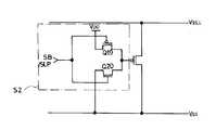
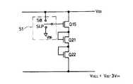
도 4는 제 1 내지 제 2 제어수단인 동작모드 제어부의 구성예를 나타낸 회로도이다.4 is a circuit diagram showing an example of the configuration of an operation mode control unit which is the first to second control means.
먼저 도 4(a)는 제 1 전압강하 수단인 엔모스 트랜지스터(Q15)를 스탠바이 모드와 슬립모드에 따라 온·오프 제어하기 위한 동작모드 제어부(S1)를 나타낸 회로도이다. 피모스 트랜지스터(Q17)와 엔모스 트랜지스터(Q18)의 각각의 드레인이 상호 연결되어 출력단을 형성한다. 피모스 트랜지스터(Q17)의 소스는 전원전압(VDD) 단자에 연결되고, 엔모스 트랜지스터(Q18)의 소스는 접지전압(VSS) 단자에 연결된다. 피모스 트랜지스터(Q17)와 엔모스 트랜지스터(Q18)의 각각의 게이트는 반전된 스탠바이 신호(/SB) 또는 슬립 신호(SLP)에 의해 제어되는데 실제로 두 신호는 같은 논리값의 신호이다.First, FIG. 4A is a circuit diagram of an operation mode controller S1 for controlling ON / OFF of the NMOS transistor Q15 as the first voltage drop means in accordance with the standby mode and the sleep mode. The drains of the PMOS transistor Q17 and the NMOS transistor Q18 are connected to each other to form an output terminal. The source of the PMOS transistor Q17 is connected to the power supply voltage VDD terminal, and the source of the NMOS transistor Q18 is connected to the ground voltage VSS terminal. Each gate of the PMOS transistor Q17 and the NMOS transistor Q18 is controlled by an inverted standby signal / SB or a sleep signal SLP. In fact, the two signals are signals having the same logic value.
스탠바이 모드로 전환되어 스탠바이 신호(SB)가 하이 레벨로 되면(이때 슬립 신호 SLP는 로우레벨이다) 반전된 스탠바이 신호(/SB)는 로우 레벨이 되어 엔모스 트랜지스터(Q18)는 턴 오프되고, 피모스 트랜지스터(Q17)는 턴 온된다. 따라서 전압강하 수단인 엔모스 트랜지스터(Q15)는 하이 레벨의 전원전압(VDD)에 의해 턴 온된다. 슬립 모드로 전환된 경우에는 슬립 신호(SLP)가 하이 레벨로 되어(이때 스탠바이 신호 SB는 로우레벨이다) 피모스 트랜지스터(Q17)는 턴 오프되고, 엔모스 트랜지스터(Q18)는 턴 온되어 전압강하 수단인 엔모스 트랜지스터(Q15)는 로우 레벨의 접지전압(VSS)에 의해 턴 오프된다.When the standby signal SB is turned to the high level (the sleep signal SLP is at the low level), the inverted standby signal / SB is at the low level, and the NMOS transistor Q18 is turned off. The MOS transistor Q17 is turned on. Therefore, the NMOS transistor Q15, which is a voltage drop means, is turned on by the high level power supply voltage VDD . When the sleep mode is switched to the sleep mode, the sleep signal SLP is at a high level (at this time, the standby signal SB is at a low level), and the PMOS transistor Q17 is turned off, and the NMOS transistor Q18 is turned on to drop the voltage. The NMOS transistor Q15, which is a means, is turned off by the low level ground voltage VSS .
도 4(b)는 제 2 전압강하 수단인 피모스 트랜지스터(Q16)를 스탠바이 모드와 슬립모드에 따라 온·오프 제어하기 위한 동작모드 제어부(S2)를 나타낸 회로도이다. 피모스 트랜지스터(Q19)와 엔모스 트랜지스터(Q20)의 각각의 드레인이 상호 연결되어 출력단을 형성한다. 피모스 트랜지스터(Q19)의 소스는 전원전압(VDD) 단자에 연결되고, 엔모스 트랜지스터(Q20)의 소스는 접지전압(VSS) 단자에 연결된다. 피모스 트랜지스터(Q19)와 엔모스 트랜지스터(Q20)의 각각의 게이트는 스탠바이 신호(SB) 또는 반전된 슬립 신호(SLP)에 의해 제어되는데 실제로 두 신호는 같은 논리값의 신호이다.FIG. 4B is a circuit diagram showing an operation mode control unit S2 for controlling the PMOS transistor Q16, which is the second voltage drop means, to be turned on and off according to the standby mode and the sleep mode. Drains of the PMOS transistor Q19 and the NMOS transistor Q20 are connected to each other to form an output terminal. The source of the PMOS transistor Q19 is connected to the power supply voltage VDD terminal, and the source of the NMOS transistor Q20 is connected to the ground voltage VSS terminal. Each gate of the PMOS transistor Q19 and the NMOS transistor Q20 is controlled by a standby signal SB or an inverted sleep signal SLP. In fact, the two signals are signals having the same logic value.
스탠바이 모드로 전환되어 스탠바이 신호(SB)가 하이 레벨로 되면(이때 슬립 신호 SLP는 로우레벨이다) 피모스 트랜지스터(Q19)는 턴 오프되고, 엔모스 트랜지스터(Q20)는 턴 온된다. 따라서 전압강하 수단인 피모스 트랜지스터(Q16)는 로우 레벨의 접지전압(VSS)에 의해 턴 온된다. 슬립 모드로 전환된 경우에는 슬립 신호(SLP)가 하이 레벨로 되어(이때 스탠바이 신호 SB는 로우레벨이다) 반전된 슬립 신호(/SLP)는 로우 레벨이 되어 엔모스 트랜지스터(Q20)는 턴 오프되고, 피모스 트랜지스터(Q19)는 턴 온되어 전압강하 수단인 피모스 트랜지스터(Q16)는 하이 레벨의 전원전압(VDD)에 의해 턴 오프된다.When the standby signal SB is turned to the high level (the sleep signal SLP is at the low level), the PMOS transistor Q19 is turned off and the NMOS transistor Q20 is turned on. Therefore, the PMOS transistor Q16, which is a voltage drop means, is turned on by the low level ground voltage VSS . When the sleep mode is switched to the sleep mode, the sleep signal SLP is at a high level (the standby signal SB is at a low level). The inverted sleep signal / SLP is at a low level, and the NMOS transistor Q20 is turned off. The PMOS transistor Q19 is turned on, and the PMOS transistor Q16, which is a voltage drop means, is turned off by the high level power supply voltage VDD .
이와 같은 동작모드 제어부(S1)(S2)에 의해 제어됨으로써 소정의 전압강하를 발생시키는 전압강하 수단(Q15)(Q16)의 구성을 달리하여 전압강하되는 크기를 제어할 수 있다. 도 5는 본 발명에 따른 전력소비 억제회로의 또 다른 전압강하 수단의 구성예를 나타낸 회로도이다.By controlling by the operation mode control unit (S1) (S2) as described above it is possible to control the magnitude of the voltage drop by changing the configuration of the voltage drop means (Q15) (Q16) for generating a predetermined voltage drop. 5 is a circuit diagram showing an example of the configuration of another voltage drop means of the power consumption suppression circuit according to the present invention.
도 5(a)는 전원전압(VDD)을 전압강하시켜 국부전원전압(VDD_L)을 발생시키기 위한 전압강하 수단의 구성예를 나타낸 것이다. 전원전압(VDD) 단자와 국부전원전압(VDD_L) 단자 사이에 세 개의 엔모스 트랜지스터(Q15)(Q21)(Q22)가 직렬 연결된다. 두 개의 엔모스 트랜지스터(Q21)(Q22)는 게이트와 드레인이 상호 연결되어 있다. 또 다른 엔모스 트랜지스터(Q15)는 동작모드 제어부(S1)에 의해 온·오프 제어되며, 엔모스 트랜지스터(Q15)가 턴 온되면 국부전원전압(VDD_L)은 VDD_L=VDD-3Vtn이 된다. 이와 같이 직렬 연결되는 엔모스 트랜지스터의 수에 따라 국부전원전압(VDD_L)의 크기가 결정되는 것이다.Fig. 5A shows an example of the configuration of voltage drop means for generating a local power supply voltage VDD_L by dropping the power supply voltage VDD . Three NMOS transistors Q15, Q21 and Q22 are connected in series between the power supply voltage VDD terminal and the local power supply voltage VDD_L terminal. The two NMOS transistors Q21 and Q22 have a gate and a drain connected to each other. The other NMOS transistor Q15 is controlled on and off by the operation mode controller S1. When the NMOS transistor Q15 is turned on, the local power supply voltage VDD_L ischanged to VDD_L = VDD -3Vtn . do. As described above, the size of the local power supply voltage VDD_L is determined according to the number of NMOS transistors connected in series.
도 5(b)는 접지전압(VSS)을 전압강하(실제로는 승압이 된다)시켜 국부접지전압(VSS_L)을 발생시키기 위한 전압강하 수단의 구성예를 나타낸 것이다. 전원전압(VSS) 단자와 국부접지전압(VSS_L) 단자 사이에 세 개의 피모스 트랜지스터(Q16)(Q23)(Q24)가 직렬 연결된다. 두 개의 엔모스 트랜지스터(Q23)(Q24)는 게이트와 드레인이 상호 연결되어 있다. 또 다른 피모스 트랜지스터(Q16)는 동작모드 제어부(S2)에 의해 온·오프 제어된다. 피모스 트랜지스터(Q16)가 턴 온되면 국부접지전압(VSS_L)은 VSS_L=VSS+3Vtp이 된다. 이와 같이 직렬 연결되는 피모스 트랜지스터의 수에 따라 국부접지전압(VSS_L)의 크기가 결정되는 것이다.Fig. 5 (b) shows an example of the configuration of voltage drop means for generating a local ground voltage VSS_L by dropping the ground voltage VSS (actually boosting). Three PMOS transistors Q16, Q23 and Q24 are connected in series between the power supply voltage VSS terminal and the local ground voltage VSS_L terminal. The two NMOS transistors Q23 and Q24 have a gate and a drain connected to each other. The other PMOS transistor Q16 is controlled on and off by the operation mode control unit S2. When the PMOS transistor Q16 is turned on, the local ground voltage VSS_L becomes VSS_L = VSS + 3Vtp . The magnitude of the local ground voltage VSS_L is determined according to the number of PMOS transistors connected in series.
이와같은 본 발명의 작용을 설명하면 다음과 같다. 활성화 모드가 진행중인 상태(ACT가 하이레벨)에서 일정시간동안 외부 조작 또는 소정의 제어신호가 발생하지 않으면 활성화 신호(ACT)가 로우 레벨로 되어 스탠바이 모드 또는 슬립모드로 전환된다. 활성화 모드에서는 곧바로 슬립모드로 전환되지는 않고 먼저 스탠바이 모드로 전환된다. 스탠바이 모드는 외부 조작이나 제어신호가 발생하지 않는 시간이 비교적 단기간일 때 진행되는 동작모드이다. 따라서 이 모드에서는 활성화 모드로 전환될 확률이 매우 높기 때문에 전압강하수단의 임계전압을 비교적 낮게 형성하여 활성화 모드로 전환되는 속도를 빠르게 한다. 즉 전력소비 억제력이 충분하지 못한 대신 동작속도의 손실을 억제할 수 있는 것이다. 만약 이와같은 스탠바이 모드가 일정시간(비교적 장시간) 이상 지속되면 활성화 모드로 전환될 확률이 매우 낮은 것으로 판단하여 동작모드를 슬립모드로 전환한다. 슬립모드로 전환하게 되면 스위칭 소자와 전압강하수단이 모두 턴 오프된다. 따라서 차후 활성화 모드로 전환할 때 다소 긴 시간이 소요되긴 하지만 전력소비는 거의 발생하지 않기 때문에, 동작속도의 손실을 감수하는 대신 전력소비 억제력을 크게 향상시킬 수 있다.Referring to the operation of the present invention as follows. When no external operation or a predetermined control signal is generated for a predetermined time while the activation mode is in progress (ACT is high level), the activation signal ACT becomes low level and is switched to the standby mode or the sleep mode. In the active mode, the system does not go to sleep immediately, but first goes into standby mode. The standby mode is an operation mode that is performed when a time when external operation or a control signal is not generated is relatively short. Therefore, in this mode, since the probability of switching to the activation mode is very high, the threshold voltage of the voltage drop means is formed relatively low, thereby speeding up the transition to the activation mode. In other words, it is possible to suppress the loss of operating speed instead of insufficient power consumption suppression. If the standby mode lasts for a predetermined time (comparatively long time), it is determined that the probability of switching to the activation mode is very low, and the operation mode is switched to the sleep mode. When switching to the sleep mode, both the switching element and the voltage drop means are turned off. Therefore, it takes a long time to switch to the active mode in the future, but the power consumption is rarely generated, it is possible to greatly improve the power consumption suppression instead of taking the loss of the operating speed.
따라서 본 발명은 회로의 동작모드를 활성화 모드와 스탠바이 모드, 슬립 모드로 구분하고 각 모드에 따라 공급전압의 크기를 차별화할 수 있는 제어수단을 구비하여, 각 동작 모드에 따른 양호한 전력소비 억제력과 스탠바이 모드에서 활성화 모드로 복귀할 때의 빠른 동작속도를 모두 만족하는 전력소비 억제회로를 청구항 1 내지 청구항 9의 발명을 통하여 구현하였다. 특히 청구항 2 내지 청구항 5의 발명을 통하여 스탠바이 모드와 슬립 모드에 따라 국부전원전압의 레벨을 제어하도록 하였으며, 청구항 6 내지 청구항 9의 발명을 통하여 스탠바이 모드와 슬립 모드에 따라 국부접지전압의 레벨을 제어하도록 함으로써, 각 동작 모드에 따른 양호한 전력소비 억제력과 스탠바이 모드에서 활성화 모드로 복귀할 때의 빠른 동작속도를 충실히 구현한 것이다.Therefore, the present invention comprises a control means for dividing the operation mode of the circuit into an activation mode, a standby mode, and a sleep mode, and to differentiate the magnitude of the supply voltage according to each mode, thereby providing good power consumption suppression force and standby power according to each operation mode. The power consumption suppression circuit that satisfies all of the fast operating speed when returning from the active mode to the active mode is implemented through the invention of
Claims (9)
Translated fromKoreanPriority Applications (3)
| Application Number | Priority Date | Filing Date | Title |
|---|---|---|---|
| KR1019970063285AKR100269643B1 (en) | 1997-11-27 | 1997-11-27 | Power reduction circuit |
| US09/154,172US6049245A (en) | 1997-11-27 | 1998-09-16 | Power reduction circuit |
| JP10328998AJPH11261400A (en) | 1997-11-27 | 1998-11-19 | Power consumption suppressing circuit |
Applications Claiming Priority (1)
| Application Number | Priority Date | Filing Date | Title |
|---|---|---|---|
| KR1019970063285AKR100269643B1 (en) | 1997-11-27 | 1997-11-27 | Power reduction circuit |
Publications (2)
| Publication Number | Publication Date |
|---|---|
| KR19990042470A KR19990042470A (en) | 1999-06-15 |
| KR100269643B1true KR100269643B1 (en) | 2000-10-16 |
Family
ID=19525721
Family Applications (1)
| Application Number | Title | Priority Date | Filing Date |
|---|---|---|---|
| KR1019970063285AExpired - Fee RelatedKR100269643B1 (en) | 1997-11-27 | 1997-11-27 | Power reduction circuit |
Country Status (3)
| Country | Link |
|---|---|
| US (1) | US6049245A (en) |
| JP (1) | JPH11261400A (en) |
| KR (1) | KR100269643B1 (en) |
Families Citing this family (54)
| Publication number | Priority date | Publication date | Assignee | Title |
|---|---|---|---|---|
| JP3080062B2 (en)* | 1998-04-06 | 2000-08-21 | 日本電気株式会社 | Semiconductor integrated circuit |
| JP4390305B2 (en)* | 1999-01-04 | 2009-12-24 | 株式会社ルネサステクノロジ | Semiconductor device |
| US6166985A (en)* | 1999-04-30 | 2000-12-26 | Intel Corporation | Integrated circuit low leakage power circuitry for use with an advanced CMOS process |
| JP3439412B2 (en)* | 1999-09-17 | 2003-08-25 | Necエレクトロニクス株式会社 | Integrated circuit device, electronic circuit device, circuit manufacturing method |
| US6333671B1 (en)* | 1999-11-03 | 2001-12-25 | International Business Machines Corporation | Sleep mode VDD detune for power reduction |
| JP2002197867A (en)* | 2000-12-28 | 2002-07-12 | Nec Corp | Semiconductor device |
| DE10120790A1 (en)* | 2001-04-27 | 2002-11-21 | Infineon Technologies Ag | Circuit arrangement for reducing the supply voltage of a circuit part and method for activating a circuit part |
| US6759873B2 (en) | 2001-05-22 | 2004-07-06 | The Board Of Trustees Of The University Of Illinois | Reverse biasing logic circuit |
| US6946901B2 (en)* | 2001-05-22 | 2005-09-20 | The Regents Of The University Of California | Low-power high-performance integrated circuit and related methods |
| US6518826B2 (en)* | 2001-06-28 | 2003-02-11 | Intel Corporation | Method and apparatus for dynamic leakage control |
| US6552596B2 (en)* | 2001-08-10 | 2003-04-22 | Micron Technology, Inc. | Current saving mode for input buffers |
| JP2003110022A (en)* | 2001-09-28 | 2003-04-11 | Mitsubishi Electric Corp | Semiconductor integrated circuit |
| KR100542398B1 (en)* | 2001-12-04 | 2006-01-10 | 주식회사 하이닉스반도체 | Voltage supply circuit |
| AU2003223386A1 (en)* | 2002-03-27 | 2003-10-13 | The Regents Of The University Of California | Low-power high-performance memory cell and related methods |
| US6801061B2 (en) | 2002-08-29 | 2004-10-05 | Micron Technology, Inc. | Reduced current input buffer circuit |
| JP3681063B2 (en)* | 2002-10-04 | 2005-08-10 | 松下電器産業株式会社 | Bias potential generator |
| JP2004186666A (en)* | 2002-10-09 | 2004-07-02 | Fujitsu Ltd | Semiconductor integrated circuit device |
| JP4122954B2 (en)* | 2002-12-06 | 2008-07-23 | 沖電気工業株式会社 | Semiconductor integrated circuit |
| US7053692B2 (en)* | 2002-12-19 | 2006-05-30 | United Memories, Inc. | Powergate control using boosted and negative voltages |
| JP4388274B2 (en)* | 2002-12-24 | 2009-12-24 | 株式会社ルネサステクノロジ | Semiconductor memory device |
| US6977519B2 (en)* | 2003-05-14 | 2005-12-20 | International Business Machines Corporation | Digital logic with reduced leakage |
| US7170327B2 (en)* | 2003-06-27 | 2007-01-30 | Intel Corporation | System and method for data retention with reduced leakage current |
| US7359277B2 (en)* | 2003-09-04 | 2008-04-15 | United Memories, Inc. | High speed power-gating technique for integrated circuit devices incorporating a sleep mode of operation |
| US7248522B2 (en)* | 2003-09-04 | 2007-07-24 | United Memories, Inc. | Sense amplifier power-gating technique for integrated circuit memory devices and those devices incorporating embedded dynamic random access memory (DRAM) |
| US7372765B2 (en)* | 2003-09-04 | 2008-05-13 | United Memories, Inc. | Power-gating system and method for integrated circuit devices |
| JP4435553B2 (en)* | 2003-12-12 | 2010-03-17 | パナソニック株式会社 | Semiconductor device |
| JP4496069B2 (en)* | 2004-12-20 | 2010-07-07 | 株式会社東芝 | MOS type semiconductor integrated circuit device |
| US7259986B2 (en)* | 2005-03-25 | 2007-08-21 | International Business Machines Corporation | Circuits and methods for providing low voltage, high performance register files |
| JP4261507B2 (en)* | 2005-03-31 | 2009-04-30 | 富士通マイクロエレクトロニクス株式会社 | Clock network power consumption reduction circuit |
| US7274217B2 (en)* | 2005-04-07 | 2007-09-25 | International Business Machines Corporation | High performance PFET header in hybrid orientation technology for leakage reduction in digital CMOS VLSI designs |
| US7262631B2 (en)* | 2005-04-11 | 2007-08-28 | Arm Limited | Method and apparatus for controlling a voltage level |
| US20070152745A1 (en)* | 2005-12-30 | 2007-07-05 | Taiwan Semiconductor Manufacturing Co., Ltd. | System and method for reducing leakage current of an integrated circuit |
| JP4911988B2 (en)* | 2006-02-24 | 2012-04-04 | ルネサスエレクトロニクス株式会社 | Semiconductor device |
| US7385435B2 (en)* | 2006-06-29 | 2008-06-10 | Intel Corporation | Programmable power gating circuit |
| JP4199793B2 (en)* | 2006-09-13 | 2008-12-17 | エルピーダメモリ株式会社 | Semiconductor device |
| JP2008098353A (en)* | 2006-10-11 | 2008-04-24 | Nec Electronics Corp | Semiconductor integrated circuit |
| US7863971B1 (en)* | 2006-11-27 | 2011-01-04 | Cypress Semiconductor Corporation | Configurable power controller |
| US7671663B2 (en)* | 2006-12-12 | 2010-03-02 | Texas Instruments Incorporated | Tunable voltage controller for a sub-circuit and method of operating the same |
| TWI373753B (en)* | 2007-03-26 | 2012-10-01 | Himax Tech Ltd | Driving circuit |
| EP2178115B1 (en)* | 2007-08-09 | 2017-12-13 | Fujitsu Limited | Semiconductor integrated circuit |
| JP4737646B2 (en)* | 2007-11-12 | 2011-08-03 | ルネサスエレクトロニクス株式会社 | Semiconductor integrated circuit device |
| US7619440B2 (en)* | 2008-01-30 | 2009-11-17 | Freescale Semiconductor, Inc. | Circuit having logic state retention during power-down and method therefor |
| DE102008053533A1 (en)* | 2008-10-28 | 2010-04-29 | Atmel Automotive Gmbh | Circuit, method for controlling and using a circuit for a sleep mode and an operating mode |
| US7969219B2 (en)* | 2008-11-26 | 2011-06-28 | Texas Instruments Incorporated | Wide range delay cell |
| JP5575405B2 (en)* | 2009-01-22 | 2014-08-20 | ピーエスフォー ルクスコ エスエイアールエル | Semiconductor device |
| US8406075B2 (en)* | 2009-04-03 | 2013-03-26 | Taiwan Semiconductor Manufacturing Company, Ltd. | Ultra-low leakage memory architecture |
| US8717093B2 (en)* | 2010-01-08 | 2014-05-06 | Mindspeed Technologies, Inc. | System on chip power management through package configuration |
| KR20120090513A (en)* | 2011-02-08 | 2012-08-17 | 삼성전자주식회사 | Semiconductor circuit having function of power gating and semiconductor device including the same |
| JP5116127B2 (en)* | 2011-03-28 | 2013-01-09 | ルネサスエレクトロニクス株式会社 | Semiconductor device |
| US9766827B1 (en)* | 2016-05-10 | 2017-09-19 | Intel Corporation | Apparatus for data retention and supply noise mitigation using clamps |
| US10262985B2 (en)* | 2016-05-10 | 2019-04-16 | Perceptia Ip Pty Ltd | Circuits and methods for lowering leakage in ultra-low-power MOS integrated circuits |
| CN111817699A (en)* | 2019-04-12 | 2020-10-23 | 三星电子株式会社 | Integrated circuits including power-gated cells |
| KR102336930B1 (en)* | 2020-09-25 | 2021-12-08 | 화인칩스 주식회사 | apparatus for reducing standby leakage current |
| JP2023062282A (en)* | 2021-10-21 | 2023-05-08 | ローム株式会社 | Switch device, electronic equipment, and vehicle |
Family Cites Families (5)
| Publication number | Priority date | Publication date | Assignee | Title |
|---|---|---|---|---|
| KR100254134B1 (en)* | 1991-11-08 | 2000-04-15 | 나시모토 류우조오 | Semiconductor integrated circuit having current reduction circuit in the standby state |
| US5614847A (en)* | 1992-04-14 | 1997-03-25 | Hitachi, Ltd. | Semiconductor integrated circuit device having power reduction mechanism |
| US5583457A (en)* | 1992-04-14 | 1996-12-10 | Hitachi, Ltd. | Semiconductor integrated circuit device having power reduction mechanism |
| EP0739097B1 (en)* | 1995-04-21 | 2004-04-07 | Nippon Telegraph And Telephone Corporation | MOSFET circuit and CMOS logic circuit using the same |
| JP2931776B2 (en)* | 1995-08-21 | 1999-08-09 | 三菱電機株式会社 | Semiconductor integrated circuit |
- 1997
- 1997-11-27KRKR1019970063285Apatent/KR100269643B1/ennot_activeExpired - Fee Related
- 1998
- 1998-09-16USUS09/154,172patent/US6049245A/ennot_activeExpired - Lifetime
- 1998-11-19JPJP10328998Apatent/JPH11261400A/enactivePending
Also Published As
| Publication number | Publication date |
|---|---|
| KR19990042470A (en) | 1999-06-15 |
| JPH11261400A (en) | 1999-09-24 |
| US6049245A (en) | 2000-04-11 |
Similar Documents
| Publication | Publication Date | Title |
|---|---|---|
| KR100269643B1 (en) | Power reduction circuit | |
| US5726562A (en) | Semiconductor device and power supply controller for same | |
| EP0212584B1 (en) | Output circuit device with stabilized potential | |
| US6448812B1 (en) | Pull up/pull down logic for holding a defined value during power down mode | |
| US6593795B2 (en) | Level adjustment circuit and data output circuit thereof | |
| US6194952B1 (en) | Transmission gate circuit | |
| KR100558549B1 (en) | Semiconductor device having an external power supply voltage control function and control method accordingly | |
| US5598107A (en) | Current switching circuit having reduced current noise operation | |
| KR100186344B1 (en) | Hysteresis Input Buffer | |
| US6720794B2 (en) | Output buffer circuit | |
| KR19990044240A (en) | Output buffer with shared intermediate node | |
| US6249146B1 (en) | MOS output buffer with overvoltage protection circuitry | |
| EP1083659B1 (en) | Level shifter | |
| US6970032B1 (en) | Power supply detecting input receiver circuit and method | |
| MXPA06011865A (en) | Break before make predriver and level-shifter. | |
| KR100344865B1 (en) | Sense amplifier | |
| US5767696A (en) | Tri-state devices having exclusive gate output control | |
| KR100660899B1 (en) | Fuse Circuit Eliminates Leakage Current Path | |
| US6329842B1 (en) | Output circuit for electronic devices | |
| JP3272809B2 (en) | Semiconductor integrated circuit device | |
| JP3602216B2 (en) | Semiconductor device | |
| KR0167261B1 (en) | The control circuit for power supply | |
| JP2912158B2 (en) | Signal line switching circuit | |
| KR100234873B1 (en) | Clock signal input buffer | |
| KR20020001634A (en) | Output buffer circuit |
Legal Events
| Date | Code | Title | Description |
|---|---|---|---|
| A201 | Request for examination | ||
| PA0109 | Patent application | St.27 status event code:A-0-1-A10-A12-nap-PA0109 | |
| PA0201 | Request for examination | St.27 status event code:A-1-2-D10-D11-exm-PA0201 | |
| R17-X000 | Change to representative recorded | St.27 status event code:A-3-3-R10-R17-oth-X000 | |
| PG1501 | Laying open of application | St.27 status event code:A-1-1-Q10-Q12-nap-PG1501 | |
| PN2301 | Change of applicant | St.27 status event code:A-3-3-R10-R13-asn-PN2301 St.27 status event code:A-3-3-R10-R11-asn-PN2301 | |
| E902 | Notification of reason for refusal | ||
| PE0902 | Notice of grounds for rejection | St.27 status event code:A-1-2-D10-D21-exm-PE0902 | |
| P11-X000 | Amendment of application requested | St.27 status event code:A-2-2-P10-P11-nap-X000 | |
| P13-X000 | Application amended | St.27 status event code:A-2-2-P10-P13-nap-X000 | |
| E701 | Decision to grant or registration of patent right | ||
| PE0701 | Decision of registration | St.27 status event code:A-1-2-D10-D22-exm-PE0701 | |
| GRNT | Written decision to grant | ||
| PR0701 | Registration of establishment | St.27 status event code:A-2-4-F10-F11-exm-PR0701 | |
| PR1002 | Payment of registration fee | St.27 status event code:A-2-2-U10-U11-oth-PR1002 Fee payment year number:1 | |
| PG1601 | Publication of registration | St.27 status event code:A-4-4-Q10-Q13-nap-PG1601 | |
| PR1001 | Payment of annual fee | St.27 status event code:A-4-4-U10-U11-oth-PR1001 Fee payment year number:4 | |
| PR1001 | Payment of annual fee | St.27 status event code:A-4-4-U10-U11-oth-PR1001 Fee payment year number:5 | |
| PN2301 | Change of applicant | St.27 status event code:A-5-5-R10-R11-asn-PN2301 | |
| PN2301 | Change of applicant | St.27 status event code:A-5-5-R10-R14-asn-PN2301 | |
| PN2301 | Change of applicant | St.27 status event code:A-5-5-R10-R11-asn-PN2301 | |
| PN2301 | Change of applicant | St.27 status event code:A-5-5-R10-R14-asn-PN2301 | |
| S20-X000 | Security interest recorded | St.27 status event code:A-4-4-S10-S20-lic-X000 | |
| PR1001 | Payment of annual fee | St.27 status event code:A-4-4-U10-U11-oth-PR1001 Fee payment year number:6 | |
| PR1001 | Payment of annual fee | St.27 status event code:A-4-4-U10-U11-oth-PR1001 Fee payment year number:7 | |
| PR1001 | Payment of annual fee | St.27 status event code:A-4-4-U10-U11-oth-PR1001 Fee payment year number:8 | |
| PR1001 | Payment of annual fee | St.27 status event code:A-4-4-U10-U11-oth-PR1001 Fee payment year number:9 | |
| PR1001 | Payment of annual fee | St.27 status event code:A-4-4-U10-U11-oth-PR1001 Fee payment year number:10 | |
| PR1001 | Payment of annual fee | St.27 status event code:A-4-4-U10-U11-oth-PR1001 Fee payment year number:11 | |
| S22-X000 | Recordation of security interest cancelled | St.27 status event code:A-4-4-S10-S22-lic-X000 | |
| PR1001 | Payment of annual fee | St.27 status event code:A-4-4-U10-U11-oth-PR1001 Fee payment year number:12 | |
| PR1001 | Payment of annual fee | St.27 status event code:A-4-4-U10-U11-oth-PR1001 Fee payment year number:13 | |
| FPAY | Annual fee payment | Payment date:20130620 Year of fee payment:14 | |
| PR1001 | Payment of annual fee | St.27 status event code:A-4-4-U10-U11-oth-PR1001 Fee payment year number:14 | |
| FPAY | Annual fee payment | Payment date:20140618 Year of fee payment:15 | |
| PR1001 | Payment of annual fee | St.27 status event code:A-4-4-U10-U11-oth-PR1001 Fee payment year number:15 | |
| FPAY | Annual fee payment | Payment date:20150617 Year of fee payment:16 | |
| PR1001 | Payment of annual fee | St.27 status event code:A-4-4-U10-U11-oth-PR1001 Fee payment year number:16 | |
| FPAY | Annual fee payment | Payment date:20160620 Year of fee payment:17 | |
| PR1001 | Payment of annual fee | St.27 status event code:A-4-4-U10-U11-oth-PR1001 Fee payment year number:17 | |
| LAPS | Lapse due to unpaid annual fee | ||
| PC1903 | Unpaid annual fee | St.27 status event code:A-4-4-U10-U13-oth-PC1903 Not in force date:20170722 Payment event data comment text:Termination Category : DEFAULT_OF_REGISTRATION_FEE | |
| PC1903 | Unpaid annual fee | St.27 status event code:N-4-6-H10-H13-oth-PC1903 Ip right cessation event data comment text:Termination Category : DEFAULT_OF_REGISTRATION_FEE Not in force date:20170722 |